
Ultrafast carrier dynamics and layer-dependent carrier recombination rate in InSe†
Ting-Hsuan
Wu
 ab,
Hao-Yu
Cheng
abc,
Wei-Chiao
Lai
b,
Raman
Sankar
b,
Chia-Seng
Chang
*ab and
Kung-Hsuan
Lin
*b
ab,
Hao-Yu
Cheng
abc,
Wei-Chiao
Lai
b,
Raman
Sankar
b,
Chia-Seng
Chang
*ab and
Kung-Hsuan
Lin
*b
aDepartment of Physics, National Taiwan University, Taipei 106319, Taiwan
bInstitute of Physics, Academia Sinica, Taipei 115201, Taiwan. E-mail: jasonc@phys.sinica.edu.tw; linkh@sinica.edu.tw
cNano-Science and Technology Program, Taiwan International Graduate Program, Academia Sinica, Taipei 115201, Taiwan
First published on 3rd January 2023
Abstract
InSe layered semiconductors with high mobility have advantages over transition-metal dichalcogenides in certain device applications. Understanding the dynamics of carriers, especially around the major bandgaps, is not only of fundamental interest but also important for improving the performance of devices. We investigated ultrafast carrier dynamics in exfoliated InSe near the bandgap and found that the presence of photocarriers led to shrinkage in the optical bandgap. In addition, we observed that the carrier recombination rate increased when the thickness of the InSe nanoflakes was reduced and the process was dominated by surface recombination. For the same flakes, the recombination rate became lower after the freshly exfoliated InSe was exposed to air and oxidized. Using a free carrier diffusion model, layer-dependent surface recombination velocities were obtained. Our investigation reveals that the surface condition and the thickness of few-layer InSe play important roles in carrier lifetimes.
Introduction
Two-dimensional (2D) layered materials that possess weak inter-layer van der Waals forces have attracted a lot of attention since graphene was successfully exfoliated from graphite crystals in 2004.1 Beyond graphene of zero bandgap, transition-metal dichalcogenides (TMDs) with a range of energy bandgaps show promising potential in electronic and optoelectronic devices2,3 and have become the most widely studied 2D layered semiconductors. However, the carrier mobility of TMD (<103 cm2 V−1 s−1) is relatively low in contrast with graphene (>104 cm2 V−1 s−1).4 In the 1980s, indium selenide (InSe) single crystals were found to possess a high carrier mobility of ∼104 cm2 V−1 s−1 at room temperature.5 They were also a candidate material for solar cells since their bandgap (∼1.24 eV) meets the maximum theoretical efficiency according to the Shockley–Queisser limit.6,7 In recent years, InSe has attracted renewed attention and the layer dependence of electrical, optical, and mechanical properties has been investigated.8 2D layered InSe has demonstrated excellent performance for nanoscale devices such as field-effect transistors with high mobility9 and photodetectors with high gains and broadband spectral responses.10–13 The carrier mobility of atomically thick InSe was demonstrated to exceed 103 cm2 V−1 s−1 at room temperature9,14 and could be even higher than 104 cm2 V−1 s−1 at liquid helium temperature.14 Few-layer InSe has also been applied in non-volatile memory,15,16 photovoltaics,17,18 and thermoelectric devices.19,20Understanding carrier dynamics is not only of fundamental scientific interest but also of importance for improving the performance of devices.21–30 For example, hot carrier cooling dynamics should be understood for hot carrier photovoltaics with a power conversion efficiency above the Shockley–Queisser limit.21,22 The photoinduced changes in the bandgap, due to bandgap renormalization and band filling effects,23–25 play important roles in optoelectronic devices such as solar cells and photodetectors. Carrier recombination is associated with the light emitting efficiency, photoconductivity, and carrier mobility of devices.26–30 Despite various kinds of devices based on few-layer InSe having been investigated in recent years, understanding of its carrier dynamics is still low. A few recent works investigated the dynamics of photocarriers associated with B-exciton transition around 2.4 eV (from the deeper valence subband edge to the conduction band edge).31,32 However, the carrier dynamics of InSe associated with the bandgap (or A-exciton) transition around 1.24 eV has not been explored, albeit the carriers around the band edges actually underline the transport properties of devices.
In this work, we utilized pump–probe reflection spectroscopy to study the ultrafast carrier dynamics in exfoliated InSe near the A-exciton transition. The presence of photocarriers induces renormalization and causes the bandgap to shrink. Meanwhile, the thermalization of hot carriers leads to a variation in the optical bandgap within 15 ps via the band filling effect. We also found that the carrier recombination rate increases with the decreasing thickness of InSe nanoflakes. For the same nanoflakes, the recombination rate of freshly exfoliated InSe is higher than that of those oxidized in air. By using a free carrier diffusion model, the layer dependence surface recombination velocities (SRVs) were obtained, which also indicated the surface recombination process was dominant.
Results and discussion
InSe flakes were prepared on polydimethylsiloxane (PDMS) substrates by mechanical exfoliation from a γ-InSe crystal. The exfoliated InSe was characterized by photoluminescence (PL) and optical transmission measurements at room temperature. Details can be found in the ESI.† The PL peak is at 1.241 eV as shown in Fig. S1(a).† Based on the fitting results of the absorption spectrum in Fig. S1(b),† the bandgap and transition energy of A-exciton are 1.239 eV and 1.229 eV, respectively. The direct bandgap of ∼1.24 eV from the valence band (VB) maximum to the conduction band (CB) minimum at the Γ point agrees with the previous reports.33–36Pump–probe reflection spectroscopy was performed to study ultrafast carrier dynamics in the InSe flakes on PDMS substrates. The detailed experimental configuration is described in the ESI.† It was confirmed that the PDMS substrate contributes to no signals under our experimental conditions. Fig. 1(a) reveals the differential reflection signal ΔR/R as a function of the pump–probe delay time for probe central energy varying from 1.20 eV to 1.38 eV. The energy of the pump beam was double that of the probe energy. For all traces, the photoexcited carrier density was kept to ∼5 × 1017 cm−3. Since the binding energy of the A-exciton was estimated to be 10 meV as described in the ESI,† the dynamics of ΔR/R should be dominated by free carriers rather than excitons at room temperature. As shown in Fig. 1(a), two main features are noticeable. First, the traces were fit by a fast exponential decay function and a slow step-like function. Since the carriers were excited with photon energy much larger than the bandgap, the fast relaxation process could be attributed to the thermalization process of hot carriers. After the carriers were relaxed to the proximity of the band edges, the step-like function could be attributed to the lifetime of the carriers. The recombination time of the carriers is longer than the observation time of 20 ps as shown in Fig. 1(a). Second, the sign of ΔR/R is sensitive to the probe energy. When the probe energy is below the bandgap of ∼1.24 eV, the responses are positive. Otherwise, they become negative.
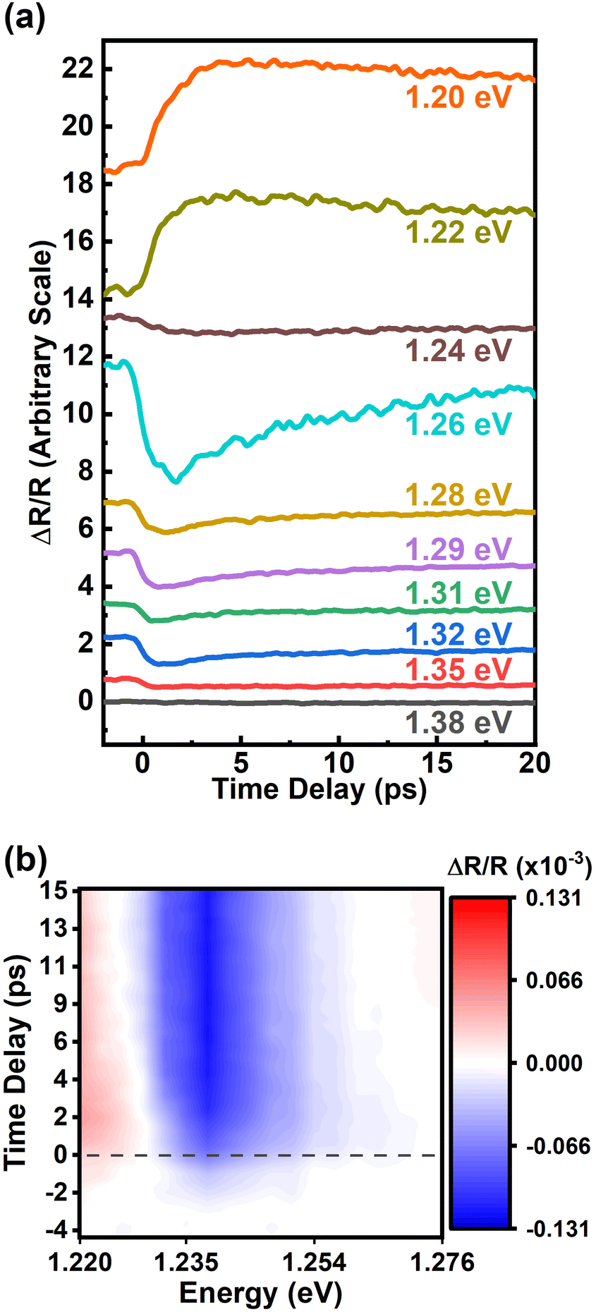 | ||
| Fig. 1 Time-resolved reflectivity changes of InSe near the bandgap energies. (a) Time-resolved reflectivity changes with different probe energies. (b) Pseudocolor 2D map of reflectivity changes as a function of probe energy and pump–probe delayed time. | ||
We further sent the probe pulse centered at 1.24 eV to a monochromator for measurements with high spectral resolution. For the detailed experimental setup refer to the ESI.† Under excitation with a pump pulse centered at 2.48 eV, the temporal responses of ΔR/R from 1.220 eV to 1.247 eV are individually shown in Fig. S2.† The data are presented with a pseudocolor 2D map as shown in Fig. 1(b). The red color represents the positive response while the blue color indicates the negative response. At zero time delay as indicated by the dashed line, the white color reveals that the photon energy for sign inversion is ∼1.230 eV. While the time delay increases, the sign inversion energy exhibits a slight red shift.
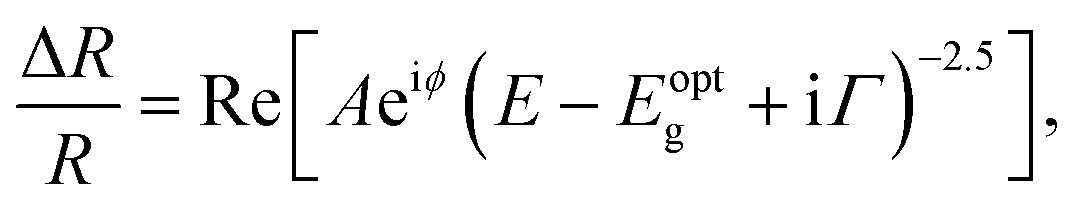
Fig. 2(a) reveals the spectral responses at 1 ps and 5 ps in Fig. 1(b), respectively. They exhibit derivative-like spectral features and are consistent with a direct interband optical transition. The spectral responses can be fit with a photoreflectance model,37–39 which considers the real part of the dielectric function for unbound charge carriers having a third-derivative behaviour with homogeneous broadening. A third-derivative line shape function appropriate for the band-to-band transition can thus be described as
 | (1) |
 | ||
| Fig. 2 Hot carrier dynamics in InSe. Spectra of the reflectivity changes fit with a third-derivative line shape function (a) for a carrier density of 5 × 1017 cm−3 and delay times of 1 ps and 5 ps, respectively, and (b) for a delay time of 1 ps and carrier densities of 5 × 1017 cm−3 and 1 × 1018 cm−3, respectively. (c) Schematic of hot carrier relaxation and bandgap renormalization. The blue arrow represents pump excitation, and the horizontal dashed lines mark the intrinsic bandgap energy Eg. | ||
Regarding slow relaxation components much longer than 20 ps, we found that the carrier lifetimes are flake dependent, which might be owing to extrinsic effects such as thickness and surface oxidation.14,41 To systematically study carrier recombination dynamics, ultrafast pump–probe micro-spectroscopy42 was performed on InSe nanoflakes with different thicknesses in a vacuum chamber. The detailed experimental setup is described in the ESI.† The optical spot size of ∼1 μm enabled us to study micron-sized InSe flakes as shown by the optical and AFM images in Fig. S3.† The photon energy of the pump/probe was around 1.6 eV, which could lessen the effect of hot carrier relaxation. It was also confirmed from Fig. S4† that the carrier lifetimes probed at 1.61 eV and 1.24 eV are the same. Fig. 3(a) shows a few representative traces of freshly exfoliated InSe nanoflakes with different thicknesses. The experimental data were fit by a single-exponential decay function as shown in the solid lines. The lifetime decreases with decreasing thickness. After the samples were exposed to air for over a month, the same nanoflakes were measured again as shown in Fig. 3(b). The trend of lifetime dependence on thickness is the same. However, the lifetimes of all the air-oxidized nanoflakes have increased compared with the freshly exfoliated samples, as summarized in Fig. 4(a).
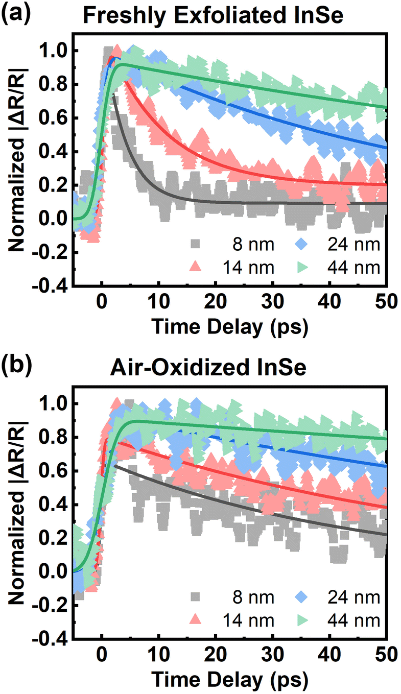 | ||
| Fig. 3 Thickness dependence on carrier recombination rate of InSe. Time-resolved reflectivity changes of (a) freshly exfoliated and (b) air-oxidized InSe for a few representative thicknesses. The solid lines reveal the fit curves with a single-exponential decay function. The pump fluence was 155 μJ cm−2. | ||
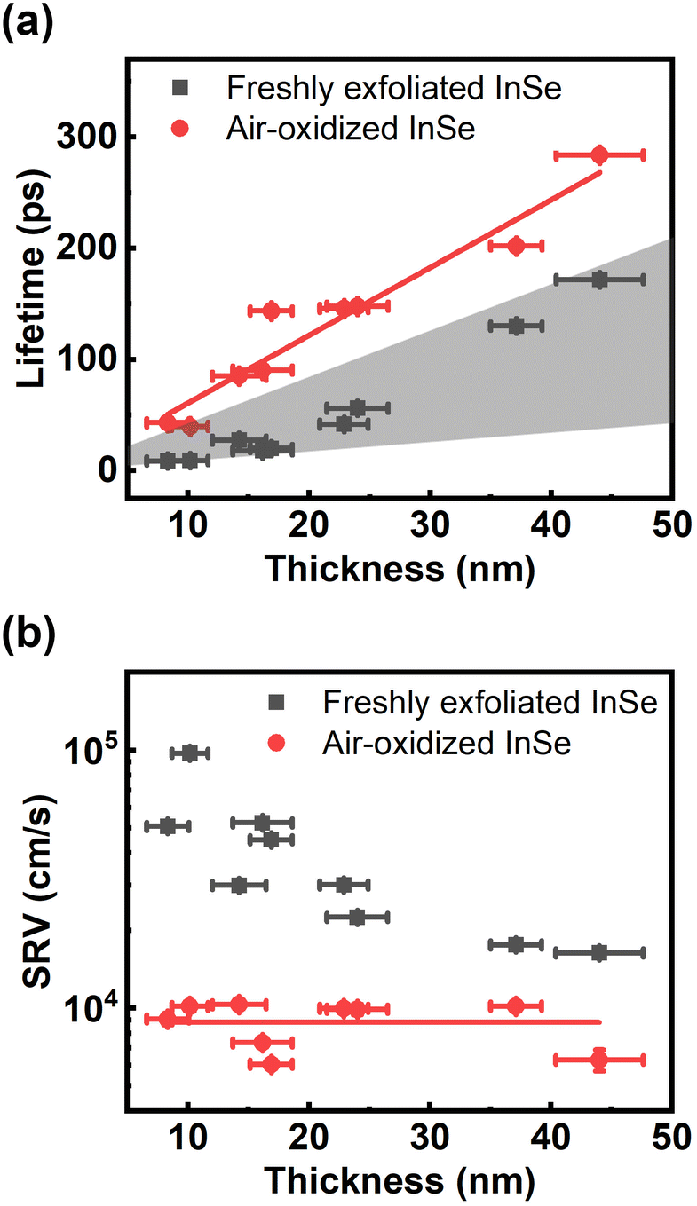 | ||
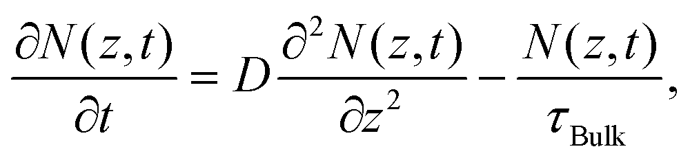
| Fig. 4 Carrier lifetimes dominated by surface recombination. Thickness dependence on (a) carrier lifetime and (b) SRV for freshly exfoliated and air-oxidized InSe. The red line indicates the linear dependence of thickness on lifetime with a constant SRV. | ||
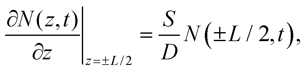
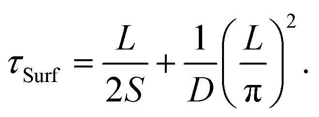
There are several mechanisms that could contribute to carrier recombination such as Auger, radiative, Shockley–Read–Hall (SRH), and surface recombination. Since the Auger and radiative processes involve two and three carriers respectively, there is a dependence of the recombination rate on carrier density.29,30 We found that the recombination rate (or lifetime) did not show any dependence on pump fluence as shown in Fig. S5,† which ruled out the Auger and radiative recombination as the dominant processes. The SRH recombination describes the trap-assisted carrier recombination in bulk semiconductors, which should be thickness independent. Therefore, surface recombination should play an important role in the thickness-dependent recombination rate in InSe nanoflakes. We used a free carrier diffusion model43–45 to quantitatively analyse the carrier dynamics of surface recombination.
The diffusion of free carriers is governed by the following equation:
 | (2) |
 | (3) |
 | (4) |
 | ||
| Fig. 5 Temporal evolution of carrier density distribution. Profiles of carrier density at different times for thickness of (a) and (c) 45 nm and (b) and (d) 1000 nm InSe, respectively. SRVs of 2 × 104 cm s−1 and 8 × 103 cm s−1 are used for (a) and (b) and (c) and (d), respectively. The time-resolved surface density at 0 nm for (e) 45 nm and (f) 1000 nm InSe, respectively. | ||
The carrier lifetime increases with increasing thickness. This tendency agrees with the experimental results in Fig. 4(a).
The free carrier diffusion model was further utilized to fit the experimental data, according to the assumption that ΔR/R is proportional to surface carrier density. In eqn. (2) and (3), S and τBulk are fitting parameters. The fitting results indicate that τBulk is long and could be set as infinity within the time window of the experimental data. That is, the bulk carrier recombination rate is extremely low compared with surface recombination. Fig. S6† shows the fitting results and the obtained SRVs are summarized in Fig. 4(b). The SRVs for freshly exfoliated InSe extend over a broad range from 1.64 × 104 cm s−1 to 9.73 × 104 cm s−1. But for air-oxidized InSe, the SRVs are much lower and more concentrated within a range between 6.06 × 103 cm s−1 and 1.01 × 104 cm s−1. Under our experimental conditions, the second term on the right-hand side of eqn (4) can be ignored. τSurf is thus proportional to L with a slope of (2S)−1. In Fig. 4(a), the solid red line depicts the linear fit with S = 8.30 × 103 cm s−1 for air-oxidized InSe. However, the thickness dependence on the lifetime could not be linearly fit with a constant SRV for freshly exfoliated InSe. The black squares in Fig. 4(b) reveal a tendency for the SRV to increase with decreasing thickness. The different features of surface recombination for freshly exfoliated and air-oxidized InSe nanoflakes can be explained as follows. During the exfoliation process, they generate Se vacancies and dangling bonds near the surface. These are trapping centres for carrier recombination in addition to surface states. When the exfoliated InSe is exposed to air, Se vacancies react with oxygen and water directly, leading to the In2O3 layer at the surface.47,48 This oxidization layer creates hole doping, which results in built-in potential and band bending around the surface.11,49,50 The charge separation of free carriers in the air-oxidized InSe therefore reduces the surface recombination rate and decreases the SRV as shown in Fig. 4. To validate this argument, we used a scanning electron microscope (SEM) to examine the freshly exfoliated and air-oxidized InSe, as shown by Fig. S7 in the ESI.† The energy-dispersive X-ray spectroscopy (EDS) indicated that the atomic percentage of the Se element is slightly lower than that of the In element in freshly exfoliated InSe, confirming the presence of Se vacancies. After the InSe sample had been exposed for over a month, an oxygen element was detected by EDS. Pump–probe measurements were also conducted in the same region of InSe examined by the EDS. The carrier lifetime of air-oxidized InSe is longer than that of freshly exfoliated InSe as shown in Fig. S7(c),† which is also consistent with the results in Fig. 3 and 4.
The mobility (μ) of a carrier is related to its lifetime (τ) and effective mass (m*) via the relation μ = eτ/m*, where e is the electron charge. The band structure of InSe with a thickness of 8 nm, which is the minimum thickness we studied in this work, has reached the bulk property.51 With a fixed value of effective mass, the mobility is proportional to the carrier lifetime and has a linear dependence on thickness. When the thickness is lower than 8 nm, a recent theoretical work indicated that both the increasing effective mass and decreasing carrier lifetime, due to the changes in the band structures and density of states, result in a dramatic reduction in mobility.51 It should also be noted that the linear dependence on carrier lifetime does not extend to infinite thickness. The carrier lifetime τ is related to the thickness-dependent lifetime τSurf of surface recombination in eqn (4) and the thickness-independent lifetime τBulk of bulk recombination via τ−1 = τSurf−1 + τBulk−1. Within 50 nm, in this work, τSurf is much shorter than τBulk and dominates the carrier lifetime. The carrier lifetime deviates from linearity when τSurf is comparable with τBulk, and saturates at τBulk in the thick region. Based on the assumption of τBulk = 1 ns, the crossover thicknesses are 400 nm and 160 nm for SRVs of 2 × 104 cm s−1 and 8 × 103 cm s−1, respectively.
Conclusions
We studied the carrier dynamics and surface recombination in InSe. The presence of photocarriers with a density of 1018 cm−3 induced bandgap renormalization and caused the gap to shrink over 12 meV. Meanwhile, the thermalization of hot carriers leads to a variation in optical bandgap of ∼1 meV within 15 ps via the band filling effect. We also found that the carrier recombination rate increases with the decreasing thickness of InSe nanoflakes. The recombination process is dominated by surface recombination when the thickness is thinner than a few tens of nanometres. The thickness and surface condition of few-layer InSe play an important role in carrier lifetimes. The carrier lifetime decreases with decreasing thickness. The surface recombination velocity can be as high as 9.73 × 104 cm s−1 for freshly exfoliated InSe but reduces to 8.30 × 103 cm s−1 in the presence of natural oxide layers on the surface. This work provides the physical insight to realize high-performance optoelectronic and photovoltaic devices based on InSe.Author contributions
K. H. L. conceived this work. K. H. L. and C. S. C. supervised this work. T. H. W. and H. Y. C. performed the optical measurements. T. H. W. and W. C. L. performed the SEM measurements. R. S. fabricated the InSe crystals. T. H. W. analysed the data. T. H. W. and K. H. L. wrote the draft. All authors have given approval for the final version of the manuscript.Conflicts of interest
There are no conflicts to declare.Acknowledgements
This work was supported by the Ministry of Science and Technology, Taiwan, under grant numbers 111-2112-M-001-087 (K. H. L.) and 110-2112-M-001-061 (C. S. C.). The authors acknowledge the resources and support from the Quantum Materials Shared Facilities of the Institute of Physics at Academia Sinica, Taiwan.References
- K. S. Novoselov, A. K. Geim, S. V. Morozov, D. Jiang, Y. Zhang, S. V. Dubonos, I. V. Grigorieva and A. A. Firsov, Science, 2004, 306, 666–669 CrossRef CAS PubMed.
- Q. H. Wang, K. Kalantar-Zadeh, A. Kis, J. N. Coleman and M. S. Strano, Nat. Nanotechnol., 2012, 7, 699–712 CrossRef CAS PubMed.
- S. Z. Butler, S. M. Hollen, L. Cao, Y. Cui, J. A. Gupta, H. R. Gutiérrez, T. F. Heinz, S. S. Hong, J. Huang, A. F. Ismach, E. Johnston-Halperin, M. Kuno, V. V. Plashnitsa, R. D. Robinson, R. S. Ruoff, S. Salahuddin, J. Shan, L. Shi, M. G. Spencer, M. Terrones, W. Windl and J. E. Goldberger, ACS Nano, 2013, 7, 2898–2926 CrossRef CAS PubMed.
- F. Schwierz, J. Pezoldt and R. Granzner, Nanoscale, 2015, 7, 8261–8283 RSC.
- A. Segura, F. Pomer, A. Cantarero, W. Krause and A. Chevy, Phys. Rev. B: Condens. Matter Mater. Phys., 1984, 29, 5708–5717 CrossRef CAS.
- W. Shockley and H. J. Queisser, J. Appl. Phys., 1961, 32, 510–519 CrossRef CAS.
- J. Martínez-Pastor, A. Segura, J. L. Valdés and A. Chevy, J. Appl. Phys., 1987, 62, 1477–1483 CrossRef.
- M. Dai, C. Gao, Q. Nie, Q.-J. Wang, Y.-F. Lin, J. Chu and W. Li, Adv. Mater. Technol., 2022, 2200321 CrossRef CAS.
- S. Sucharitakul, N. J. Goble, U. R. Kumar, R. Sankar, Z. A. Bogorad, F.-C. Chou, Y.-T. Chen and X. P. A. Gao, Nano Lett., 2015, 15, 3815–3819 CrossRef CAS PubMed.
- S. R. Tamalampudi, Y.-Y. Lu, R. K. U, R. Sankar, C.-D. Liao, K. M. B, C.-H. Cheng, F. C. Chou and Y.-T. Chen, Nano Lett., 2014, 14, 2800–2806 CrossRef CAS PubMed.
- Y.-R. Chang, P.-H. Ho, C.-Y. Wen, T.-P. Chen, S.-S. Li, J.-Y. Wang, M.-K. Li, C.-A. Tsai, R. Sankar, W.-H. Wang, P.-W. Chiu, F.-C. Chou and C.-W. Chen, ACS Photonics, 2017, 4, 2930–2936 CrossRef CAS.
- Z. Yang, W. Jie, C.-H. Mak, S. Lin, H. Lin, X. Yang, F. Yan, S. P. Lau and J. Hao, ACS Nano, 2017, 11, 4225–4236 CrossRef CAS PubMed.
- L. Liu, L. Wu, A. Wang, H. Liu, R. Ma, K. Wu, J. Chen, Z. Zhou, Y. Tian, H. Yang, C. Shen, L. Bao, Z. Qin, S. T. Pantelides and H.-J. Gao, Nano Lett., 2020, 20, 6666–6673 CrossRef CAS PubMed.
- D. A. Bandurin, A. V. Tyurnina, G. L. Yu, A. Mishchenko, V. Zólyomi, S. V. Morozov, R. K. Kumar, R. V. Gorbachev, Z. R. Kudrynskyi, S. Pezzini, Z. D. Kovalyuk, U. Zeitler, K. S. Novoselov, A. Patanè, L. Eaves, I. V. Grigorieva, V. I. Fal'ko, A. K. Geim and Y. Cao, Nat. Nanotechnol., 2017, 12, 223–227 CrossRef CAS PubMed.
- F.-S. Yang, M. Li, M.-P. Lee, I. Y. Ho, J.-Y. Chen, H. Ling, Y. Li, J.-K. Chang, S.-H. Yang, Y.-M. Chang, K.-C. Lee, Y.-C. Chou, C.-H. Ho, W. Li, C.-H. Lien and Y.-F. Lin, Nat. Commun., 2020, 11, 2972 CrossRef CAS PubMed.
- S. Wang, L. Liu, L. Gan, H. Chen, X. Hou, Y. Ding, S. Ma, D. W. Zhang and P. Zhou, Nat. Commun., 2021, 12, 53 CrossRef CAS PubMed.
- J. Wang, H. Yu and C. Hou, Nanoscale, 2021, 13, 6871–6883 RSC.
- X. Liu, J.-C. Ren, T. Shen, S. Li and W. Liu, J. Phys. Chem. Lett., 2019, 10, 7712–7718 CrossRef CAS PubMed.
- K. H. Lee, M.-W. Oh, H.-S. Kim, W. H. Shin, K. Lee, J.-H. Lim, J.-i. Kim and S.-i. Kim, Inorg. Chem. Front., 2019, 6, 1475–1481 RSC.
- N. T. Hung, A. R. T. Nugraha, T. Yang, Z. Zhang and R. Saito, J. Appl. Phys., 2018, 125, 082502 CrossRef.
- K. K. Paul, J.-H. Kim and Y. H. Lee, Nat. Rev. Phys., 2021, 3, 178–192 CrossRef CAS.
- J. M. Richter, F. Branchi, F. Valduga de Almeida Camargo, B. Zhao, R. H. Friend, G. Cerullo and F. Deschler, Nat. Commun., 2017, 8, 376 CrossRef PubMed.
- J. S. Manser and P. V. Kamat, Nat. Photonics, 2014, 8, 737–743 CrossRef CAS.
- S. Meng, J. Wang, H. Shi, X. Sun and B. Gao, Phys. Chem. Chem. Phys., 2021, 23, 24313–24318 RSC.
- A. Chernikov, C. Ruppert, H. M. Hill, A. F. Rigosi and T. F. Heinz, Nat. Photonics, 2015, 9, 466–470 CrossRef CAS.
- L. Yuan, T. Wang, T. Zhu, M. Zhou and L. Huang, J. Phys. Chem. Lett., 2017, 8, 3371–3379 CrossRef CAS PubMed.
- W. de Quilettes Dane, M. Vorpahl Sarah, D. Stranks Samuel, H. Nagaoka, E. Eperon Giles, E. Ziffer Mark, J. Snaith Henry and S. Ginger David, Science, 2015, 348, 683–686 CrossRef CAS PubMed.
- C. Jin, E. Y. Ma, O. Karni, E. C. Regan, F. Wang and T. F. Heinz, Nat. Nanotechnol., 2018, 13, 994–1003 CrossRef CAS PubMed.
- H. J. Shin, S. Bae and S. Sim, Nanoscale, 2020, 12, 22185–22191 RSC.
- I. Robel, B. A. Bunker, P. V. Kamat and M. Kuno, Nano Lett., 2006, 6, 1344–1349 CrossRef CAS PubMed.
- C. Zhong, V. K. Sangwan, J. Kang, J. Luxa, Z. Sofer, M. C. Hersam and E. A. Weiss, J. Phys. Chem. Lett., 2019, 10, 493–499 CrossRef CAS PubMed.
- Y. Li, J. Ye, K. Yuan, G. Zhai, T. Li, Y. Ye, X. Wu and X. Zhang, Nanotechnology, 2019, 31, 095713 CrossRef PubMed.
- C.-H. Ho and Y.-J. Chu, Adv. Opt. Mater., 2015, 3, 1750–1758 CrossRef CAS.
- J. Camassel, P. Merle, H. Mathieu and A. Chevy, Phys. Rev. B: Solid State, 1978, 17, 4718–4725 CrossRef CAS.
- M. V. Andriyashik, M. Yu. Sakhnovskii, V. B. Timofeev and A. S. Yakimova, Phys. Status Solidi B, 1968, 28, 277–285 CrossRef CAS.
- D. T. Do, S. D. Mahanti and C. W. Lai, Sci. Rep., 2015, 5, 17044 CrossRef CAS PubMed.
- F. Ruf, Excitonic Effects and Bandgap Instabilities in Perovskite Solar Cells, Karlsruher Institut für Technologie (KIT), 2020 Search PubMed.
- F. H. Pollak and O. J. Glembocki, Proc. SPIE, 1988, 0946, 2 CrossRef CAS.
- G. Jnawali, S. Linser, I. A. Shojaei, S. Pournia, H. E. Jackson, L. M. Smith, R. F. Need and S. D. Wilson, Nano Lett., 2018, 18, 5875–5884 CrossRef CAS PubMed.
- P. V. Kamat, N. M. Dimitrijevic and A. J. Nozik, J. Phys. Chem., 1989, 93, 2873–2875 CrossRef CAS.
- N. Balakrishnan, Z. R. Kudrynskyi, E. F. Smith, M. W. Fay, O. Makarovsky, Z. D. Kovalyuk, L. Eaves, P. H. Beton and A. Patanè, 2D Mater., 2017, 4, 025043 CrossRef.
- K.-H. Lin, H.-Y. Cheng, C.-Y. Yang, H.-W. Li, C.-W. Chang and S.-W. Chu, Appl. Phys. Lett., 2018, 113, 171906 CrossRef.
- K. L. Luke and L. J. Cheng, J. Appl. Phys., 1987, 61, 2282–2293 CrossRef CAS.
- G. S. Kousik, Z. G. Ling and P. K. Ajmera, J. Appl. Phys., 1992, 72, 141–146 CrossRef.
- M. De Laurentis and A. Irace, J. Solid State Phys., 2014, 2014, 291469 Search PubMed.
- A. B. Sproul, J. Appl. Phys., 1994, 76, 2851–2854 CrossRef CAS.
- L. Shi, Q. Zhou, Y. Zhao, Y. Ouyang, C. Ling, Q. Li and J. Wang, J. Phys. Chem. Lett., 2017, 8, 4368–4373 CrossRef CAS PubMed.
- P.-H. Ho, Y.-R. Chang, Y.-C. Chu, M.-K. Li, C.-A. Tsai, W.-H. Wang, C.-H. Ho, C.-W. Chen and P.-W. Chiu, ACS Nano, 2017, 11, 7362–7370 CrossRef CAS PubMed.
- E. Yablonovitch, D. L. Allara, C. C. Chang, T. Gmitter and T. B. Bright, Phys. Rev. Lett., 1986, 57, 249–252 CrossRef CAS PubMed.
- D. J. Michalak, F. Gstrein and N. S. Lewis, J. Phys. Chem. C, 2008, 112, 5911–5921 CrossRef CAS.
- W. Li, S. Poncé and F. Giustino, Nano Lett., 2019, 19, 1774–1781 CrossRef CAS PubMed.
Footnote |
| † Electronic supplementary information (ESI) available. See DOI: https://doi.org/10.1039/d2nr05498a |
| This journal is © The Royal Society of Chemistry 2023 |