DOI:
10.1039/D2NR05212A
(Paper)
Nanoscale, 2023,
15, 507-514
Plasmonic hot carrier injection from single gold nanoparticles into topological insulator Bi2Se3 nanoribbons†
Received
21st September 2022
, Accepted 14th November 2022
First published on 16th November 2022
Abstract
Plasmonic gold nanoparticles injecting hot carriers into the topological insulator (TI) interface of Bi2Se3 nanoribbons are studied by resonant Raman spectroscopy. We resolve the impact of individual gold particles with sizes ranging from 140 nm down to less than 40 nm on the topological surface states of the nanoribbons. In resonance at 1.96 eV (633 nm), we find distinct phonon renormalization in the Eg2- and A1g2-modes that can be associated with plasmonic hot carrier injection. The phonon modes are strongly enhanced by a factor of 350 when tuning the excitation wavelengths into interband transition and in resonance with the surface plasmon of gold nanoparticles. At 633 nm wavelength, a plasmonic enhancement factor of 18 is observed indicating a contribution of hot carriers injected from the gold nanoparticles into the TI interface. Raman studies as a function of gold nanoparticle size reveal the strongest hot carrier injection for particles with size of 108 nm in agreement with the resonance energy of its surface plasmon. Hot carrier injection opens the opportunity to locally control the electronic properties of the TI by metal nanoparticles attached to the surface of nanoribbons.
Introduction
Topological insulators (TIs) are a new set of quantum materials with conducting surface states and an insulating bulk.1 The surface states of TIs have gapless electronic states that are protected by time reversal symmetry.2–4 These surface states host quasi-relativistic electrons2,5 and are immune to backscattering by nonmagnetic impurities due to strong spin–orbit coupling.2,6 TIs with their spin-textured surface states find applications in quantum computing, spintronics, photonics, fibre lasers, and optoelectronic devices.7–10 Bismuth selenide (Bi2Se3) is considered an ideal candidate for realizing intriguing phenomena associated with TIs due to its surface state band structure of Dirac-like linear dispersion with a bulk energy band gap of about 0.3 eV, which is significantly larger than the room temperature energy scale of around 25 meV.6,11 Moreover, the Dirac point of Bi2Se3 is supposed to be within the bulk bandgap and not buried in the bulk bands as in bismuth telluride (Bi2Te3) and antimony telluride (Sb2Te3). Device applications requiring Dirac materials demand detailed understanding of the role of contacts and carrier injection in controlling their relativistic surface states.8,12 The interface between the conducting surface states of Bi2Se3 and metals has been theoretically studied.13,14 Most of these theories are concerned with the generation of hot plasmonic carriers and their injection into the semiconductors interface and molecular surfaces.15,16 Remarkably, contacting the surface of Bi2Se3 with gold thin films does not destroy the spin-momentum locking in Bi2Se3.13 Gold nanoparticles (AuNPs) have a large number of delocalized electrons, which can interact with electromagnetic fields to generate surface plasmons17 which exhibit a large absorption cross section that has been exploited to enhance and trap light.15 The resonantly excited surface plasmons change the optical properties of AuNPs drastically and can decay non-radiatively into hot electron–hole pairs.12,18 In graphene-based devices, hot electron–hole pairs increase local electron densities and generate photocurrents.19,20 The local manipulation of relativistic quantum states of nanostructures with AuNPs is an emerging research field8,21,22 and in this fashion, the surface states of Bi2Se3 can be engineered into future device requirements by locally manipulating the electronic band structure in nanostructures.23 The hot photoinjected electrons interact with the relativistic quantum states of TIs and couple to the surface phonon modes.15 Micro-Raman spectroscopy with a high local resolution of about 200 nm enables the investigation of the local electronic properties by probing the phonons on sample scales of less than 400 nm. Furthermore, controlling the interaction of the surface states with hot photoinjected electrons by means of an electromagnetic field opens the opportunity to control the local electronic properties of TIs optically. Spatially resolved micro-Raman spectroscopy is as an excellent tool for simultaneously studying the generation of electron–hole pairs and detection of the corresponding electron–phonon interaction.12
In this work, we probe the local area around AuNPs which are not easily accessible in the electrical transport measurement. We locally manipulate the electronic structure of 1D nanostructures (nanoribbons) of Bi2Se3 with single AuNPs and use the phonon modes in Bi2Se3 as local probes of the modified relativistic surface state. The interplay between the electronic surface states of a single crystalline Bi2Se3 nanoribbon and resonantly excited plasmons in a AuNP is studied by micro-Raman spectroscopy with spatial resolution of 211 nm (see Fig. S7 in the ESI(F)† for details). Different sizes of AuNPs on the same Bi2Se3 nanoribbon were employed to locally manipulate the electronic band structure. We scan across single AuNPs deposited on a Bi2Se3 nanoribbon in order to determine the changes in electron–phonon interactions as a function of distance from the respective AuNP and reveal the phonon self-energy effect due to electrons injected into the relativistic surface state.
Results and discussion
Bi2Se3 with its layered, rhombohedral crystal structure belongs to the space group (R![[3 with combining macron]](https://www.rsc.org/images/entities/char_0033_0304.gif) m/D53d).6,24–26 Its structure consists of five atomic layers, Se–Bi–Se–Bi–Se, that are covalently stacked along its c-axis to form a quintuple layer with a thickness of ∼1 nm. The unit cell of Bi2Se3 contains three quintuple layers and each quintuple layer is bound to neighbouring quintuple layers by van der Waals forces. Group theory predicts the five atoms in the primitive cell of Bi2Se3 to have 15 zone-centre phonon branches, 3 acoustic and 12 optical phonon modes. Of the 12 optical modes, 4 are symmetry Raman-active (2A1g, 2Eg) and 4 are symmetry infrared-active (2A1u, 2Eu). The irreducible representations for the zone-centre phonon can be written as: Γ = 2Eg + 2A1g + 2Eu + 2A1u [1].25 The Raman tensors and their corresponding atomic displacements of the Raman-active modes in Bi2Se3 are shown in Fig. S6 (in the ESI(E)).† The correct stoichiometry (2
m/D53d).6,24–26 Its structure consists of five atomic layers, Se–Bi–Se–Bi–Se, that are covalently stacked along its c-axis to form a quintuple layer with a thickness of ∼1 nm. The unit cell of Bi2Se3 contains three quintuple layers and each quintuple layer is bound to neighbouring quintuple layers by van der Waals forces. Group theory predicts the five atoms in the primitive cell of Bi2Se3 to have 15 zone-centre phonon branches, 3 acoustic and 12 optical phonon modes. Of the 12 optical modes, 4 are symmetry Raman-active (2A1g, 2Eg) and 4 are symmetry infrared-active (2A1u, 2Eu). The irreducible representations for the zone-centre phonon can be written as: Γ = 2Eg + 2A1g + 2Eu + 2A1u [1].25 The Raman tensors and their corresponding atomic displacements of the Raman-active modes in Bi2Se3 are shown in Fig. S6 (in the ESI(E)).† The correct stoichiometry (2![[thin space (1/6-em)]](https://www.rsc.org/images/entities/char_2009.gif) :3 (Bi:Se)) of the nanoribbons is confirmed by SEM-EDX (see Fig. S4 in the ESI(D)†). SEM and AFM studies shown in the inset (Fig. 1 and 3) and the ESI† support the reported width and thickness of the nanoribbons, respectively (Fig. S5 in the ESI(D)†).
:3 (Bi:Se)) of the nanoribbons is confirmed by SEM-EDX (see Fig. S4 in the ESI(D)†). SEM and AFM studies shown in the inset (Fig. 1 and 3) and the ESI† support the reported width and thickness of the nanoribbons, respectively (Fig. S5 in the ESI(D)†).
 |
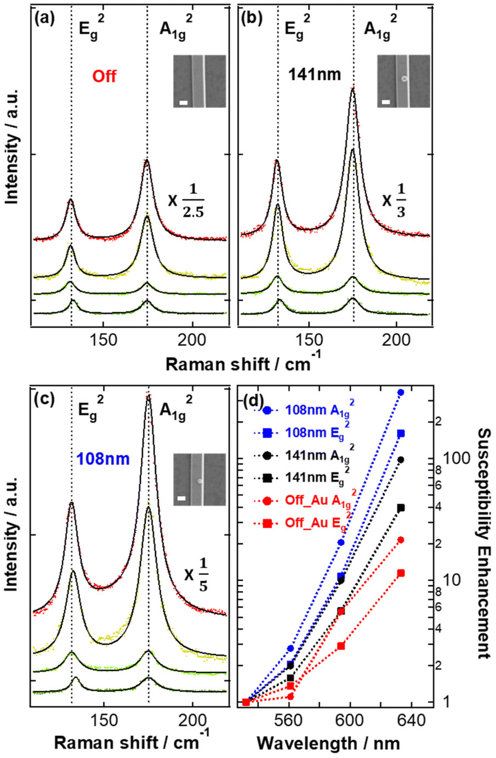
| | Fig. 1 Resonance Raman spectra of a single Bi2Se3 nanoribbon with a thickness of 100 nm and width of 210 nm decorated with gold nanoparticles (AuNPs) of the following diameters: (a) Off_AuNP, i.e. spectrum recorded far away from any AuNP, (b) 141 nm, and (c) 108 nm. The Raman spectra taken with 633, 594, 561, and 533 nm are shown in red, yellow, light green, and green, respectively. The solid black line represents the fit to the data and the dashed vertical lines represent the positions of the respective Eg2 and A1g2-modes in the Bi2Se3 nanoribbon taken with 633 nm. The data obtained for 633 nm excitation of the 108 nm AuNP, the 141 nm AuNP, and Off_AuNPs is divided by 5, 3 and 2.5, respectively, as indicated in panels (a–c). The insets in panels (a–c) show the SEM images of the studied sample area. Each scale bar represents a length of 200 nm (d) Phonon susceptibilities as a function of excitation wavelengths normalized to the phonon susceptibility at 532 nm. The blue, black, and red markers correspond to the measurements on 108 nm AuNP, 141 nm AuNP, and Off_AuNP respectively. Square and circle markers correspond to Eg2 and A1g2-modes, respectively. | |
The in- and off-resonance study of a single Bi2Se3 nanoribbon decorated with AuNPs is shown in Fig. 1. Fig. 1(a–c) shows the Raman spectra of a single Bi2Se3 nanoribbon decorated with a 108 nm AuNP, a 141 nm AuNP, and Off_AuNP in the laser focus (=Off_AuNP, i.e. spectrum recorded far away from any AuNP) at different excitation wavelengths. We can assign the two distinct phonon modes to Eg2 and A1g2 symmetry27–29 and the assignment is supported by the Raman tensor in Fig. S6(a) (ESI)† as well as the polarization-dependent data in Fig. S8 (ESI†). The spectra were fitted with eqn (1) (“Generalized Fano equation”).30
| |  | (1) |
with
where
Ā,
y,
![[q with combining macron]](https://www.rsc.org/images/entities/i_char_0071_0304.gif)
,
ω0,
![[capital Gamma, Greek, macron]](https://www.rsc.org/images/entities/i_char_e0ba.gif)
,
g and
T represent the amplitude, electronics background, ratio between imaginary and real parts of the electronic susceptibility, frequency, width of phonon line, electron–phonon coupling, and electron–photon coupling, respectively. π
im and π
re are the imaginary and real part of electronic susceptibility while A
2 is the non-resonant matrix element.
53 All data were corrected for the scattering volume and the spectral response of the instrument.
31Fig. 1(d) shows the relative phonon susceptibilities of 108 nm AuNP, 141 nm AuNP, and Off_AuNP as a function of the excitation wavelength
λ. The phonon susceptibilities were normalized to the susceptibility at 532 nm wavelength. The circle and square markers correspond to the A
1g2 and the E
g2 mode, respectively. As we tune the excitation wavelength into resonance of the nanoribbon (from 532 nm to 633 nm), the Raman signal increases by a factor of 20 for the A
1g2 mode and a factor of 11 for the E
g2 mode (red symbols) in the Off_Au position. This resonance has been reported previously and it is attributed to interband transitions in Bi
2Se
3.
26,32–34 We observe that tuning the excitation wavelength into resonance when measuring on the 141 nm AuNP results in a further increase in the Raman signal by a factor of 98 for A
1g2 mode and a factor of 40 for the E
g2 mode (black symbols). We attribute the enhancement of the Raman signal to the hot carrier injection into the Bi
2Se
3 TI. Our reference measurements on silicon substrate decorated with AuNPs support our attribute (see Fig. S10 in the ESI(I)
†). A similar behaviour has been observed in graphene.
12 Surprisingly, measuring on 108 nm AuNP results in a signal enhancement factor of more than 350 for the A
1g2 mode and a factor of 160 for the E
g2 mode (blue symbol). The plasmonic enhancement factor at 633 nm excitation wavelength on 141 nm and 108 nm AuNP is 5 and 18 for A
1g2 mode, respectively and the corresponding plasmonic enhancement factor for E
g2 mode is 3.6 and 15, respectively. Note that without the capping layer on AuNP, we would expect stronger hot carrier injection.
54,55 The Raman spectra in
Fig. 1 were measured on the same Bi
2Se
3 nanoribbon with the differently sized AuNPs spaced more than 2.2 μm apart from each other. Hot carriers are efficiently excited when the localized surface plasmon (LSP) of AuNP is in resonance with the excitation wavelength.
35 By means of Landau damping, the excited hot carriers decay non-radiatively into hot electron–hole pairs.
36 Note that non-radiative decay can occur either through intraband excitations within the sp (conduction) band above the Fermi level or through interband transition from d-band to s-band.
37,38 The density of generated hot carriers and excitation rate in metallic surface plasmons was theoretically studied by Paudel
et al.14 and it was observed that the density of the generated hot carriers scales with the square of the excitation rate.
14 The data in
Fig. 1 reveals the strongest hot carrier injection into the Bi
2Se
3 nanoribbon by 108 nm AuNP which can be explained by the resonance energy of its surface plasmon in the red wavelength range.
39–41 We show that the presence of AuNPs, more especially AuNP whose LSP is in resonance with the excitation wavelength, on Bi
2Se
3 strongly enhances the Raman signal and thus opens an opportunity to control the local electronic properties of the TI by different sizes of AuNP. Furthermore, we conducted measurements in the vicinity of an AuNP with 633 nm excitation wavelength as shown in
Fig. 2. We scanned across a single AuNP on a Bi
2Se
3 nanoribbon from −900 to +900 nm with the AuNP at 0 nm (
Fig. 2(b)).
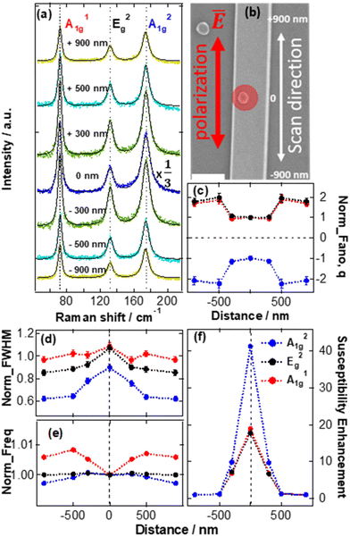 |
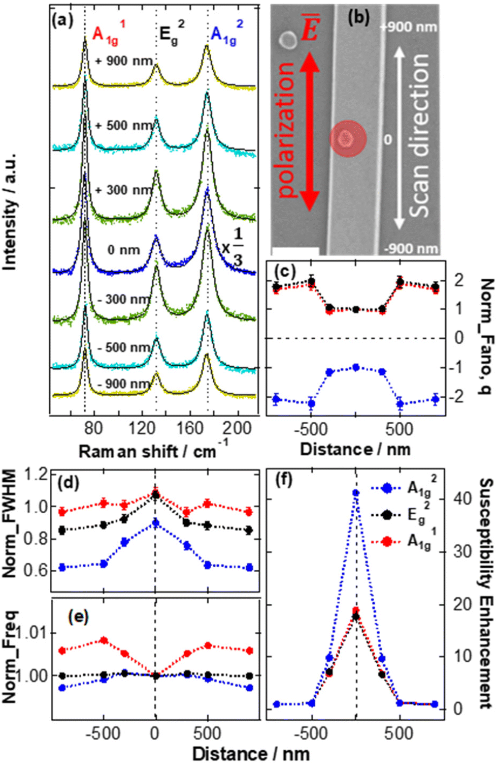
| | Fig. 2 Raman studies of single Bi2Se3 nanoribbon in the vicinity of AuNP with 633 nm excitation wavelength. (a) Raman spectra of Bi2Se3 nanoribbon of thickness 76.3 nm and width 400 nm and decorated with a single 120 nm AuNP. The spectra were collected scanning across the nanoribbon in different distance to the AuNP from −900 to +900 nm as shown in (a). The black vertical dashed lines represent the positions of A1g1, Eg2 and A1g2 modes of the bare nanoribbon. The data obtained at the AuNP position is divided by 3 as indicated in the panel (a). (b) SEM image of the studied nanoribbon with the AuNP. The red and white arrows represent the polarization of the laser and the scan direction. (c) Fano parameter, , (d) Norm_FWHM (normalized full width at half maximum), (e) Norm_Freq (normalized frequency) and (f) susceptibility enhancement as a function of the distance from the AuNP. All normalized to the value at the On_AuNP (0 nm) position. The vertical and horizontal dashed lines represent guide to the eye. | |
Fig. 2(a) shows the Raman spectra while moving the focus of the laser beam away from the AuNP, i.e. scanning along the nanoribbon. We can assign the three distinct phonon modes to A1g1, Eg2, and A1g2 symmetry. All three modes show strong characteristic enhancements in the vicinity of the AuNP and the enhancement decays when moving the focus of the laser beam away from the AuNP. Fig. 2(b) shows the SEM image of the measured sample. The scan direction is depicted by the white double-headed arrow. The polarization of the laser is along the long axis of the Bi2Se3 nanoribbon as shown by the double-headed red arrow. The phonon modes were fitted with the generalized Fano line shape described by eqn (1). Fig. 2(c) displays the normalized Fano parameter, as a function of distance from the AuNP. The Fano parameter implies the interference between discrete phonon states and low-energy electronic degrees of freedom.42 The smaller the , the stronger the effective interference between electrons and phonons due to an increased contribution of the imaginary part of the electronics susceptibility. We reveal that is smaller for On_Au position than Off_Au position. This indicates that the electron–phonon interaction is much stronger when measuring at the On_Au position than measuring at the Off_Au position. Fig. 2(d) shows the normalized full width at half maximum (FWHM) as a function of the distance from the AuNP. We observe broadening of the three phonon modes as we scan towards the AuNP due to high density of hot electrons, in the vicinity of AuNP, which interact with the phonons. The density of the hot carriers injected into the Bi2Se3 TI at the AuNP/TI interface decreases with the distance from the AuNP. This is corroborated by the small value of Fano parameter for On_Au position and the ratio between the FWHM of A1g2/A1g1 (Eg2/A1g1) mode that increases from 1.77 (1.60) to 2.28 (1.83) at the AuNP position (see Fig. S9 in the ESI(H)†). Such a decrease of the phonon lifetime (peak broadening) of the Bi2Se3 modes has been observed previously and attributed to a strong electron–phonon coupling.6 Our observation of high density of hot electrons near the AuNP and a reduced one away from AuNP is supported by the theoretical study of carrier distribution on the surface of the Bi2Se3 TI at different length scales after the hot carrier injection by Paudel et al.14 Furthermore, we observe phonon renormalization of the A1g1 and A1g2 modes when scanning across the AuNP (Fig. 2(e)). The scan-related renormalization of the phonon modes has been observed in graphene and attributed to the coupling of the optical phonon modes at specific wave vectors with hot electrons transferred upon resonant excitation of AuNPs plasmons.12Fig. 2(f) reveals the Raman susceptibility enhancement when scanning across the AuNP. The Raman susceptibility enhancement factor of 19, 18, and 41, for A1g1, Eg2, and A1g2 modes, respectively, is obtained when measuring at the On_AuNP position. In short, the observed Raman susceptibility enhancement shows that the presence of AuNPs enhances the Raman scattering by injection of hot electrons from the AuNP into Bi2Se3.
In Fig. 3 we present the study of four different sizes of AuNPs on a single Bi2Se3 nanoribbon. The Raman spectra are shown in Fig. 3(a). The insets are the SEM images of 39, 50, 120, and 147 nm size AuNPs and each scale bar represents a length of 100 nm. The spectra were fitted with the generalized Fano eqn (1). Line shape analysis of the Raman spectra reveals an asymmetric Fano profile depending on the diameter of the AuNP (Fig. 3(b)). We like to recall that the Fano parameter measures the interference between the phonon states and electronic degrees of freedom. We further observe a hardening of the A1g2 mode mostly in 39 and 50 nm AuNPs (Fig. 3(c)) as indicated by the blue shift in this mode. The frequency shift originates from the interaction of phonon mode with the real part of the low energy electronic susceptibility of the injected hot carriers from plasmonic AuNPs. The mutual interaction of plasmons with phonons leads to phonon renormalization. This renormalization of phonon modes is the result of interactions of the phonons with surface plasmon polaritons. Similar effects have been reported previously in the periodic arrays of ribbons of Bi2Se3.43,44 In Fig. 3(d), we show the normalized FWHM as a function of the diameter of AuNPs. Our result shows no noticeable dependence of FWHM on the size of AuNPs.
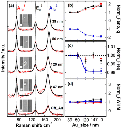 |
| | Fig. 3 Raman studies of a single Bi2Se3 nanoribbon decorated with AuNPs of different sizes. (a) Raman spectra of a Bi2Se3 nanoribbon with thickness of 90.1 nm and width of 292 nm and decorated with four different AuNPs of sizes 39, 50, 120, and 147 nm. The insets in (a) show the SEM images. Each scale bar represents a length of 100 nm. The black vertical dashed lines indicate the positions of A1g1, Eg2 and A1g2 modes without AuNPs present. (b) Fano parameter (c) Frequency and (d) FWHM as a function of the AuNP diameter. All plotted line-width parameters are normalized to the value of the 39 nm AuNP. The horizontal dashed line represents a guide to the eye. | |
Plasmonic decay and hot electron transfer
Fig. 4a shows the schematic illustration of the measured Bi2Se3 nanoribbon. The blue shaded area beneath the AuNP indicates the region of band bending which is associated with the metal/TI interface,13 note that this region has a dimension of only 3–5 nm and its lateral extent is governed by the size of the AuNP. The phonon enhancement and renormalization in our results are explained in the scheme in Fig. 4c. Laser irradiation on the AuNP leads to excitation of collective free carrier oscillations at its surface, i.e., surface plasmons. The generated plasmons in resonance with the incident light field lead to a confinement of the incident light field.45 The resonantly excited plasmons decay non-radiatively by generation of hot carriers as depicted in Fig. 4(c). The density of the generated hot carriers decreases at some distance away from the AuNP. The grey parabolic dispersion lines represent the Bi2Se3 bulk conduction band (CB) and valence band (VB) while the black linear dispersion lines represent the surface states’ CB and VB. The black thick horizontal lines represent the energy levels of the low energy phonons. The red dash line represents the Fermi energy (EF) for the bare TI. The resonantly decayed plasmons inject hot electrons into the CB (the upper Dirac cone) of the TI. There have been detailed reports on the extraction of hot charge carriers from the resonantly excited plasmons into the CBs of semiconductors.16,19,46 The transferred hot electrons populate states on the thick blue parabola in Fig. 4(c). The schematic diagram illustrates that low-energy phonons cannot interfere with the bulk electrons provided that the Fermi surface lies between the bulk CB and VB. Conversely, low-energy phonons can couple to the quasi-relativistic electrons that populate the surface states of the TI. This picture supports our observation of the coupling between the electronic degrees of freedom and the phonon states evidenced by the phonon renormalization in the vicinity of the AuNPs as explained earlier. Fig. 4(b) shows the dependence of Fano parameter on the excitation wavelength λ when measuring on the 108 nm AuNP (blue symbol) and 141 nm AuNP (black symbol). Fig. 4(b) further shows that measuring on the bare TI (red symbol), the Fano parameter has no significant dependence on the excitation wavelength. The Fano parameter represents a measure of the electronic susceptibility interacting with a phonon. The fact that this parameter is constant in the bulk but strongly wavelength dependent for the AuNPs, strongly supports a hot carrier injection mechanism. Furthermore, our observation of the strong signal enhancement by a factor of 350 on the 108 nm AuNP can be explained as double-resonance behaviour: the band structure calculations for Bi2Se3 show an interband transition energy of 2.0 eV.11,32 The 633 nm excitation wavelength (1.96 eV) that generated the surface plasmons in the 108 nm AuNP is simultaneously in resonance with the plasmon frequency of the 108 nm AuNP and also in resonance with the interband transition in Bi2Se3. This double resonance enhances hot electron transfer and consequently, the Raman scattering cross-section.
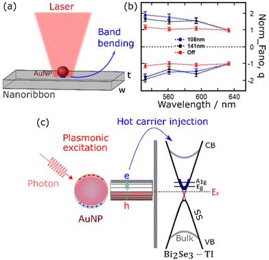 |
| | Fig. 4 (a) Schematic illustration of the TI nanoribbon decorated with a AuNP. The blue shaded area indicates the region of band bending (note that the band bended region is covered by the AuNP), the laser spot covers predominantly areas in the vicinity of the AuNP (t = thickness and w = width of the nanoribbon). (b) Fano parameter as a function of the excitation wavelength for the bare TI (red marker), 141 nm AuNP (black marker), and 108 nm AuNP (blue marker) position. All normalized to the value at 633 nm wavelength. The horizontal dashed line represents a guide to the eye. (c) The scheme for the hot carrier injection in TI. The resonantly excited plasmons of a AuNP decay by injecting hot electrons into the conduction band of TI. The grey parabolic dispersion represents the conduction band (CB) and the valence band (VB) of bulk TI. The surface state (SS) is represented by the black linear dispersion. The red dashed horizontal line represents the Fermi energy (EF) of the bare TI. The black thick horizontal lines represent the phonons. The phonons lie in the SS of the linear dispersion and interact with the injected electrons (thick blue parabola). | |
Conclusions
We have studied photoinduced doping of the topological insulator Bi2Se3 surface states by means of hot electrons generated from the decayed surface plasmons of AuNPs by nanoscopic Raman spectroscopy. We showed that the lattice dynamics in Bi2Se3 are modified in the vicinity of a gold nanoparticle. By tuning the excitation wavelength into double resonance with the plasmon frequency and interband transition in Bi2Se3, we reveal the strongest enhancement of the phonon modes by a factor of 350. Our result shows strong electron–phonon interactions and phonon renormalization induced by hot-carrier injection from the resonantly excited plasmons into the electronic surface states of the Bi2Se3. Our study provides a fundamental understanding of the interaction between electrons and phonons on the nanoscale. This insight opens the opportunity to locally investigate and control a variety of active optoelectronic and optical properties.
Methods
Single crystalline Bi2Se3 nanoribbons were grown in a two-heating zone furnace via chemical vapor deposition (CVD). The furnace was equipped with a quartz tube of diameter 2.5 cm. Bi2Se3 nanoribbons were grown on silicon 〈100〉 substrates with a native oxide (SiO2) layer. We followed the general approach in CVD method47–49 with full optimization for growth of Bi2Se3 nanoribbons (see the ESI(A)† about the experimental procedure). A custom-made x, y, z – positioner micro-manipulator was used to transfer the nanoribbons to a custom-made silicon finder grid with 225 fields of 100 μm × 100 μm. Atomic force microscopy (AFM) was utilized to measure the thickness (height) and width of the nanoribbons. Scanning electron microscope (SEM) was used to determine the position and size of the AuNPs. Energy dispersive X-ray spectroscopy (EDX) was employed to investigate the stoichiometry of the nanoribbons. The nanoribbons were decorated with single gold nanoparticles of different sizes before the Raman measurement (see ESI(C)†). For this a polydisperse solution of AuNPs with mean diameter of 96 nm was used,50 which comprise a range of different AuNP diameters (see the ESI(B)† about the synthesis and characterization of the AuNPs). By using SEM AuNPs of different size on the nanoribbons could be selected for measurements. All nanoribbons were characterized before and after the Raman study. Raman scattering spectroscopy of AuNP decorated single nanoribbons was carried out at room temperature with a custom-made piezo-controlled micro-Raman set-up.31,51 The spatial resolution of the micro-Raman is 211 nm at 633 nm excitation wavelength. The measurements were carried out in back-scattering configuration while employing Porto notation ![[Z with combining macron]](https://www.rsc.org/images/entities/i_char_005a_0304.gif) (XX)Z configuration.52 In all measurements, the polarization of the laser is parallel to the c-axis of the wire (except for polarization studies with indicated polarizations) (see the ESI(G)† about the Polarization dependence study). In order to exclude laser heating of the samples, the laser power on the sample surface was kept below 50 μW.
(XX)Z configuration.52 In all measurements, the polarization of the laser is parallel to the c-axis of the wire (except for polarization studies with indicated polarizations) (see the ESI(G)† about the Polarization dependence study). In order to exclude laser heating of the samples, the laser power on the sample surface was kept below 50 μW.
Abbreviations
| AuNPs | Gold nanoparticles |
| Tis | Topological insulators |
| LSP | Localized surface plasmon |
| CVD | Chemical vapor deposition |
| SEM | Scanning electron microscopy |
| AFM | Atomic force microscopy |
| EDX | Energy dispersive X-ray |
| VB | Valence band |
| CB | Conduction band |
| FWHM | Full width at half maximum |
| Bi2Se3 | Bismuth selenide |
Author contributions
The manuscript was written through contributions of all authors. All authors have given approval to the final version of the manuscript.
Conflicts of interest
There are no conflicts to declare.
Acknowledgements
We thank Robert Frömter for discussions on electron microscopy. Yalan Huang is supported by the Chinese Scholarship Council (CSC). Parts of this project were supported by the Cluster of Excellence ‘Advanced Imaging of Matter’ of the Deutsche Forschungsgemeinschaft (DFG) – EXC 2056 – project ID 390715994.
References
- Y. Ando, Topological insulator materials, J. Phys. Soc. Jpn., 2013, 82, 1020011–10200132, DOI:10.7566/JPSJ.82.102001.
- M. Z. Hasan and C. L. Kane, Colloquium: Topological insulators, Rev. Mod. Phys., 2010, 82, 3045–3067, DOI:10.1103/RevModPhys.82.3045.
- C. L. Kane and E. J. Mele, Z2 topological order and the quantum spin hall effect, Phys. Rev. Lett., 2005, 95, 1468021–1468024, DOI:10.1103/PhysRevLett.95.146802.
- B. A. Bernevig, T. L. Hughes and S. C. Zhang, Quantum Spin Hall Effect and Topological Phase Transition in HgTe Quantum Wells, Science, 2006, 314, 1757–1761, DOI:10.1126/science.1133734.
- X. L. Qi and S. C. Zhang, Topological insulators and superconductors, Rev. Mod. Phys., 2011, 83, 1057–1110, DOI:10.1103/RevModPhys.83.1057.
- J. Zhang, Z. Peng, A. Soni, Y. Zhao, Y. Xion, B. Peng, J. Wang, M. S. Dresselhaus and Q. Xiong, Raman spectroscopy of few-quintuple layer topological insulator Bi2Se3 nanoplatelets, Nano Lett., 2011, 11, 2407–2414, DOI:10.1021/nl200773n.
- V. Sacksteder, T. Ohtsuki and K. Kobayashi, Modification and control of topological insulator surface states using surface disorder, Phys. Rev. Appl., 2015, 3, 0640061–0640067, DOI:10.1103/PhysRevApplied.3.064006.
- M. K. Ranjuna and J. Balakrishnan, Investigating the thermal transport in gold decorated graphene by opto-thermal Raman technique, Nanotechnology, 2022, 33, 1857061–1857069, DOI:10.1088/1361-6528/ac45c2.
- C. Zhao, Y. Zou, Y. Chen, Z. Wang, S. Lu, H. Zhang, S. Wen and D. Tang, Wavelength-tunable picosecond soliton fiber laser with Topological Insulator: Bi2Se3 as a mode locker “Mode-locked fiber lasers based on a saturable absorber incorporating carbon nanotubes, J. Opt. Soc. Am., 2012, 20, 27888–27895, DOI:10.1364/OE.20.027888.
- W. Zhao, L. Chen, Z. Yue, Z. Li, D. Cortie, M. Fuhrer and X. Wang, Quantum oscillations of robust topological surface states up to 50 K in thick bulk-insulating topological insulator, npj Quantum Mater., 2019, 4, 1–6, DOI:10.1038/s41535-019-0195-7.
- H. Zhang, C. X. Liu, X. L. Qi, X. Dai, Z. Fang and S. C. Zhang, Topological insulators in Bi2Se3, Bi2Te3 and Sb2Te3 with a single Dirac cone on the surface, Nat. Phys., 2019, 5, 438–442, DOI:10.1038/nphys1270.
- M. Weinhold, S. Chatterjee and P. J. Klar, Modifying graphene's lattice dynamics by hot-electron injection from single gold nanoparticles, Commun. Phys., 2019, 2, 1–10, DOI:10.1038/s42005-019-0115-y.
- C. D. Spataru and F. Léonard, Fermi-level pinning, charge transfer, and relaxation of spin-momentum locking at metal contacts to topological insulators, Phys. Rev. B: Condens. Matter Mater. Phys., 2014, 90, 0851151–0851156, DOI:10.1103/PhysRevB.90.085115.
- H. P. Paudel, V. Apalkov, X. Sun and M. I. Stockman, Plasmon-induced hot carrier transfer to the surface of three-dimensional topological insulators, Phys. Rev. B, 2018, 98, 0754281–0754287, DOI:10.1103/PhysRevB.98.075428.
- A. O. Govorov, H. Zhang and Y. K. Gun'Ko, Theory of photoinjection of hot plasmonic carriers from metal nanostructures into semiconductors and surface molecules, J. Phys. Chem. C, 2013, 117, 16616–16631, DOI:10.1021/jp405430m.
- M. W. Knight, Y. Wang, A. S. Urban, A. Sobhani, B. Y. Zheng, P. Nordlander and N. J. Halas, Embedding Plasmonic Nanostructure Diodes Enhances Hot Electron Emission, ACS Nano Lett., 2013, 13, 1687–1692, DOI:10.1021/nl400196z.
- V. Amendola, R. Pilot, M. Frasconi, O. M. Maragò and M. A. Iatì, Surface plasmon resonance in gold nanoparticles: A review, J. Phys.: Condens. Matter, 2017, 29, 2030021–20300249, DOI:10.1088/1361-648X/aa60f3.
- L. D. Landau, On the vibration of the electronic plasma, J. Phys., 1946, 10, 25–34 Search PubMed.
- Z. Fang, Y. Wang, Z. Liu, A. Schlather, P. M. Ajayan, F. H. L. Koppens, P. Nordlander and N. J. Halas, Plasmon-induced doping of graphene, ACS Nano, 2012, 6, 10222–10228, DOI:10.1021/nn304028b.
- Z. Fang, Z. Liu, Y. Wang, P. M. Ajayan, P. Nordlander and N. J. Halas, Graphene-antenna sandwich photodetector, Nano Lett., 2012, 12, 3808–3813, DOI:10.1021/nl301774e.
- A. Scandurra, F. Ruffino, M. Censabella, A. Terrasi and M. G. Grimaldi, Dewetted Gold Nanostructures onto Exfoliated Graphene Paper as High Efficient Glucose Sensor, Nanomaterials, 2019, 9, 1794–1799, DOI:10.3390/nano9121794.
- A. Singh, G. Sharma, B. P. Singh and P. Vasa, Charge-Induced Lattice Compression in Monolayer MoS2, J. Phys. Chem. C, 2019, 123, 17943–17950, DOI:10.1021/acs.jpcc.9b02308.
- C. Z. Chang, P. Tang, X. Feng, K. Li, X. Ma, W. Duan, K. He and Q. Xue, Band Engineering of Dirac Surface States in Topological-Insulator-Based van der Waals Heterostructures, Phys. Rev. Lett., 2015, 115, 1368011–1368015, DOI:10.1103/PhysRevLett.115.136801.
- B. Irfan, S. Sahoo, A. Gaur, M. Ahmadi, M. Guine, R. Katiyar and R. Chatterjee, Temperature dependent Raman scattering studies of three-dimensional topological insulators Bi2Se3, J. Appl. Phys., 2014, 115, 1735061–1735067, DOI:10.1063/1.4871860.
- W. Richter, H. Koi-Iler and C. R. Becker, A Raman and Far-Infrared Investigation of Phonons in the Rhombohedra1 V2–V13 Compounds BigTe3, Bi2Se3, Sb2Tea and Bi2(Te14Sea)3 (0 < x < l), (Bil,Sbv)2Te3 (0 < y < 1), Phys. Status Solidi B, 1977, 84, 619–628 CrossRef CAS
https://onlinelibrary.wiley.com/doi/abs/10.1002/pssb.2220840226
.
- K. M. F. Shahil, M. Z. Hossain, V. Goyal and A. A. Balandin, Micro-Raman spectroscopy of mechanically exfoliated few-quintuple layers of Bi2Te3, Bi2Se3, and Sb2Te3 materials, J. Appl. Phys., 2012, 111, 0543051–0543058, DOI:10.1063/1.3690913.
- H. Li, H. Peng, W. Dang, L. Yu and Z. Liu, Topological insulator nanostructures: Materials synthesis, Raman spectroscopy, and transport properties, Front. Phys., 2012, 7, 208–217, DOI:10.1007/s11467-011-0199-7.
- Y. Zhao, X. Luo, J. Zhang, J. Wu, X. Bal, M. Wang, J. Jia, H. Peng, Z. Liu, S. Quek and Q. Xiong, Interlayer vibrational modes in few-quintuple-layer Bi2Te3 and Bi2Se3 two-dimensional crystals: Raman spectroscopy and first-principles studies, Phys. Rev. B: Condens. Matter Mater. Phys., 2014, 90, 2454281–24542811, DOI:10.1103/PhysRevB.90.245428.
- M. Eddrief, P. Atkinson, V. Etgens and J. Bernard, Low-temperature Raman fingerprints for few-quintuple layer topological insulator Bi2Se3 films epitaxied on GaAs, Nanotechnology, 2014, 25, 2457011–2457018 CrossRef PubMed
https://iopscience.iop.org/article/10.1088/0957-4484/25/24/245701/meta
.
-
T. E. Glier, S. Scheitz, C. Nweze and M. Ruebhausen, Inelastic light scattering to study electron-phonon interactions in Topological Insulators” Unpublished.
- B. Schulz, J. Baeckstroem, D. Budelmann, R. Maeser and M. Ruebhausen, Fully reflective deep ultraviolet to near infrared spectrometer and entrance optics for resonance Raman spectroscopy, Rev. Sci. Instrum., 2005, 76, 0731071–07310713, DOI:10.1063/1.1946985.
- P. Sharma, R. Sharma, V. Awana, T. Narayanan, B. Gupta, N. Vashistha, L. Tyagi and M. Kumar, Low-temperature ultrafast optical probing of topological bismuth selenide, J. Alloys Compd., 2021, 886, 1612351–1612359, DOI:10.1016/j.jallcom.2021.161235.
- M. Eddrief, F. Vidal and B. Gallas, Optical properties of Bi2Se3: From bulk to ultrathin films, J. Phys. D: Appl. Phys., 2016, 49, 5053041–5053010, DOI:10.1088/0022-3727/49/50/505304.
- Y. Sharma, P. Srivastava, A. Dashora, L. Vadkhiya, M. Bhayani, R. Jain, A. Jani and B. Ahuja, Electronic structure, optical properties and Compton profiles of Bi2S3 and Bi2Se3, Solid State Sci., 2012, 14, 241–249, DOI:10.1016/j.solidstatesciences.2011.11.025.
- M. L. Brongersma, N. J. Halas and P. Nordlander, Plasmon-induced hot carrier science and technology, Nat. Nanotechnol., 2015, 10, 25–34, DOI:10.1038/nnano.2014.311.
- X. Li, D. Xiao and Z. Zhang, Landau damping of quantum plasmons in metal nanostructures, New J. Phys., 2013, 15, 0230111–02301115, DOI:10.1088/1367-2630/15/2/023011.
- E. Minutella, F. Schulz and H. Lange, Excitation-dependence of plasmon-induced hot electrons in gold nanoparticles, J. Phys. Chem. Lett., 2017, 8, 4925–4929, DOI:10.1021/acs.jpclett.7b02043.
- C. Clavero, Plasmon-induced hot-electron generation at nanoparticle/metal-oxide interfaces for photovoltaic and photocatalytic devices, Nat. Photonics, 2014, 8, 95–103, DOI:10.1038/nphoton.2013.238.
- Y. Francescato, V. Giannini and A. M. Stefan, Plasmonic Systems Unveiled by Fano Resonances, ACS Nano, 2012, 6, 1830–1838, DOI:10.1021/nn2050533.
- S. Link and M. A. El-Sayed, Shape and size dependence of radiative, non-radiative and photothermal properties of gold nanocrystals, Int. Rev. Phys. Chem., 2000, 19, 409–453, DOI:10.1080/01442350050034180.
- H. S. Kim and D. Y. Lee, Near-infrared-responsive cancer photothermal and photodynamic therapy using gold nanoparticles, Polymers, 2018, 10, 9611–96114, DOI:10.3390/POLYM10090961.
- U. Fano, Effects of Configuration Interaction on Intensities and Phase Shifts, Phys. Rev., 1961, 124, 1866–1878, DOI:10.1103/PhysRev.124.1866.
- P. di Pietro, M. Ortolani, O. Limaj, A. Di Gaspare, V. Giliberti, F. Giorgianni, M. Brahlek, N. Bansal, N. Koirala, S. Oh, P. Calvani and S. Lupi, Observation of Dirac plasmons in a topological insulator, Nat. Nanotechnol., 2013, 8, 556–560, DOI:10.1038/nnano.2013.134.
- Y. Deshko, L. Krusin-Elbaum, V. Menon, A. Khanikaev and J. Trevino, Surface plasmon polaritons in topological insulator nano-films and superlattices, Opt. Express, 2016, 24, 7398–7410, DOI:10.1364/oe.24.007398.
- K. A. Willets and R. P. van Duyne, Localized surface plasmon resonance spectroscopy and sensing, Annu. Rev. Phys. Chem., 2007, 58, 267–297, DOI:10.1146/annurev.physchem.58.032806.104607.
- P. Singhal and H. N. Ghosh, Hot Charge Carrier Extraction from Semiconductor Quantum Dots, J. Phys. Chem. C, 2018, 122, 17586–17600, DOI:10.1021/acs.jpcc.8b03980.
- H. Peng, K. Lai, D. Kong, S. Meister, Y. Chen, X. Qi, S. Zhang, Z. Shen and Y. Cui, Aharonov-Bohm interference in topological insulator nanoribbons, Nat. Mater., 2010, 9, 225–229, DOI:10.1038/nmat2609.
- D. Kong, J. Randel, H. Peng, J. Cha, S. Meister, K. Lai, Y. Chen, Z. Shen, H. Manoharan and Y. Cui, Topological insulator nanowires and nanoribbons, Nano Lett., 2010, 10, 329–333, DOI:10.1021/nl903663a.
- Y. Yan, Z. Liao, Y. Zhou, H. Wu, Y. Bie, J. Chen, J. Meng, X. Wu and D. Yu, Synthesis and quantum transport properties of Bi2Se3 topological insulator nanostructures, Sci. Rep., 2013, 3, 12641–11645, DOI:10.1038/srep01264.
- J. Hühn, C. Carrillo-Carrion, M. Soliman, C. Pfeiffer, D. Valdeperez, A. Masood, I. Chakraborty, L. Zhu, M. Gallego, Z. Yue, M. Carril, N. Feliu, A. Escudero, A. Alkilany, B. Pelaz, P. Pino and W. Parak, Selected standard protocols for the synthesis, phase transfer, and characterization of inorganic colloidal nanoparticles, Chem. Mater., 2017, 29, 399–461, DOI:10.1021/acs.chemmater.6b04738.
-
T. E. Glier, Applications of Functional One-Dimensional Nanostructures Studied by Light Scattering, University of Hamburg, 2021 Search PubMed.
- T. C. Damen, S. P. Porto and B. Tell, Raman Effect in Zinc Oxide, J. Phys. Chem. Solids, 1966, 142, 570–574, DOI:10.1103/PhysRev.142.570.
- A. Bock, S. Ostertun, R. Das Sharma, M. Rübhausen, K. O. Subke and C. T. Rieck, Anomalous self-energy effects of the B1g phonon in Y1-x(Pr,Ca)xBa2Cu3O7 films, Phys. Rev. B: Condens. Matter Mater. Phys., 1999, 3532–3537, DOI:10.1103/PhysRevB.60.3532.
- H. Lee, S. Yoon, J. Jo, B. Jeon, T. Hyeon, K. An and J. Y. Park, Enhanced hot electron generation by inverse metal oxide interfaces on catalytic nanodiode, Faraday Discuss., 2019, 214, 353, 10.1039/C8FD00136G.
- J. Y. Park, H. Lee, J. R. Renzas, Y. Zhang and G. A. Somorjai, Probing hot electron flow generated on pt nanoparticles with Au/TiO2 schottky diodes during catalytic CO oxidation, Nano Lett., 2008, 8, 2388, DOI:10.1021/nl8012456.
Footnote |
| † Electronic supplementary information (ESI) available: Additional information on the Bi2Se3 nanoribbon synthesis and Au nanoparticle synthesis, transfer of ribbons, drop casting of AuNPs, AFM, EDX, and SEM image, polarization dependence study. See DOI: https://doi.org/10.1039/d2nr05212a |
|
| This journal is © The Royal Society of Chemistry 2023 |
Click here to see how this site uses Cookies. View our privacy policy here. 
 Open Access Article
 This Open Access Article is licensed under a
  *a,
Tomke E.
Glier
*a,
Tomke E.
Glier