Block copolymer self-assembly to pattern gold nanodots for site-specific placement of DNA origami and attachment of nanomaterials

Dulashani R. Ranasinghe a, Gregory Doerk b, Basu R. Aryal a, Chao Pang a, Robert C. Davis c, John N. Harb d and Adam T. Woolley *a
aDepartment of Chemistry and Biochemistry, Brigham Young University, Provo, UT, USA. E-mail: atw@byu.edu
bCenter for Functional Nanomaterials, Brookhaven National Laboratory, Upton, NY, USA
cDepartment of Physics and Astronomy, Brigham Young University, Provo, UT, USA
dDepartment of Chemical Engineering, Brigham Young University, Provo, UT, USA

Received 13th September 2022 , Accepted 27th December 2022

First published on 28th December 2022


Abstract

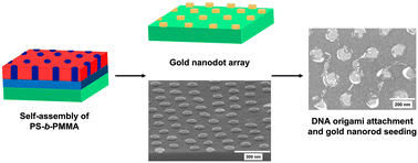
Directed placement of DNA origami could play a key role in future integrated nanoelectronic devices. Here we demonstrated the site-selective attachment of DNA origami on gold dots formed using a pattern transfer method through block copolymer self-assembly. First, a random copolymer brush layer is grafted on the Si surface and then poly (styrene-b-methylmethacrylate) block copolymer is spin-coated to give a hexagonal nanoarray after annealing. UV irradiation followed by acetic acid etching is used to remove the PMMA, creating cylindrical holes and then oxygen plasma etching removes the random copolymer layer inside those holes. Next, metal evaporation, followed by lift-off creates a gold dot array. We evaluated different ligand functionalization of Au dots, as well as DNA hybridization to attach DNA origami to the nanodots. DNA-coated Au nanorods are assembled on the DNA origami as a step towards creating nanowires and to facilitate electron microscopy characterization of the attachment of DNA origami on these Au nanodots. The DNA hybridization approach showed better DNA attachment to Au nanodots than localization by electrostatic interaction. This work contributes to the understanding of DNA-templated assembly, nanomaterials, and block copolymer nanolithography. Furthermore, the work shows potential for creating DNA-templated nanodevices and their placement in ordered arrays in future nanoelectronics.


1. Introduction

The growth of nanofabrication has led the way for innovations in various areas, including medicine, textiles, agriculture, food, and electronics.1 Some of these, including medical and energy-serving products, have already been established and marketed,2 while others like optics and nano sensing are still in the laboratory stage.3 Miniaturization allows for manufacture of portable,4 implantable,5 and even injectable devices.6 Current top-down nanofabrication techniques have been effective in meeting the global demands of increased capacity per unit area and lowered costs for improved devices. New technologies, such as 3-D integration7 and new materials for interconnects,8 will help to continue these advances. Additionally, bottom-up nanofabrication is a promising alternative to developing nanoscale designs as it is widely applicable and potentially scalable to generate large numbers of devices.9 Furthermore, bottom-up nanofabrication techniques often consume little energy,10 do not need expensive patterning tools11 and provide a fundamental platform for materials assembly and characterization.12 In bottom-up methods, self-assembly is essential as it enables the construction of complex architectures from molecular building blocks.13 Our work is centred on two types of self-assembled soft-matter systems: block copolymers (BCPs) and DNA origami.

BCPs contain two or more covalently bonded segments of different polymers. They can self-assemble into ordered structures with nanofeatures whose size can be engineered by managing the molecular weights of the individual segments.14 Nanoscale patterns that result from BCP thin films are suitable for various applications of nanofabrication, including electronics, optics, solar cells, magnetic storage, and acoustics.15

DNA origami, initially presented by Paul Rothemund in 2006,16 can create 2-D and 3-D nanoscale objects through programmed self-assembly based on hydrogen bonding between base pairs. DNA origami uses a long, single-stranded DNA (ssDNA), called the scaffold (typically viral DNA ∼7000 nucleotides long), with hundreds of designed short ssDNA called staple strands. Each staple strand has multiple binding sites that connect distant scaffold domains via crossover base pairing, folding the scaffold into desired shapes. The versatility of DNA origami templates in various applications, including medical,17 plasmonic18 and electrical,19 can be increased through functionalization with nanomaterials.20 Aryal et al.21 utilized the site-specific binding nature of DNA to fabricate plus, cross, and c-shaped structures and created metal nanowires on these shapes. By careful engineering, different materials can be attached to the same DNA origami template.22,23 In addition to hybridization, chemical24 and electrostatic interactions25 allow for nanomaterial attachment that is not DNA sequence specific. Electronic materials such as Au,26 Te,22 Ag,27 Cu28 and Pd29 have been assembled to create continuous wires. Furthermore, carbon nanotubes30 have been attached to DNA origami to create field-effect transistors with tuneable conductivity.30

Periodic arrangements of DNA-organized devices are useful for optical and electronic applications. It is common to integrate the bottom-up self-assembly of DNA structures with top-down lithographic methods for surface patterning. For example, Ding et al.31 placed DNA origami nanotubes, having multiple thiol groups near each end, on surface-patterned gold islands created by electron-beam lithography (EBL). They further demonstrated an interconnection strategy by constructing complex networks of DNA origami nanotubes whose orientation was precisely controlled by the spacing and pattern of the gold islands. Moreover, Gopinath et al.32 showed the directed self-assembly of DNA origami using electron beam patterning. They created triangular binding sites with negatively charged surface carboxylate groups surrounded by hydrophobic methyl groups. A DNA origami with fluorescent groups bound strongly on the carboxylate groups via Mg2+ bridging, and they demonstrated optical features that could be useful in nanophotonics or nanoelectronics. Gerdon et al.33 reported a method combining top-down fabrication and bottom-up self-assembly to control the delivery of individual DNA origami onto a single nanometer-scale gold pattern formed by EBL. They modified the gold with a carboxylic acid-terminated self-assembled monolayer to attract DNA origami and enable the controlled placement of nanostructures onto surfaces. Nanosphere lithography (NSL) is an alternative to EBL for patterning surfaces.34 NSL allowed nonspecific DNA origami placement where they adsorbed to exposed SiO2 by forming salt bridges with Mg2+ at the bottom of nanoholes in a Au film.35

EBL and ion-beam lithography have several deficiencies,36 including expensive equipment and maintenance and loss of design resolution because of scattering in the substrate.37 NSL can pattern only a few shapes and designs. Furthermore, NSL is restricted by the self-arrangement of spheres to drive the nanopatterning, so only homogenous repeating arrays result from this method. Although larger or smaller nanoparticles (NPs) can be generated by varying the diameter of the nanospheres, changing the in-plane NP size independently from the distance between the NPs is not straightforward.38 In order to obtain significant advantages in terms of speed, power consumption, and cost in fabrication of tiny features, researchers will need to overcome issues arising from the cost and complexity of the technology. Self-assembly of nanostructures may offer a powerful solution to these issues at sub-20 nm sizes.

BCP nanolithography refers to the use of BCPs to pattern target substrates to generate functional nanostructures in thin-film geometries. This work focuses on a BCP system composed of polystyrene (PS) and poly(methyl methacrylate) (PMMA) that spontaneously microphase-separates into a hexagonal lattice of vertical PMMA cylinders in a matrix of PS on a surface under appropriate processing conditions.39,40 The orientation of the minor and major BCP phases in thin films depends on many factors, including substrate surface energy, film thickness, roughness and topography.39 Landeke-Wilsmark et al.41 used a poly(styrene-b-2-vinylpyridine) BCP to create well-ordered, dense arrays of discrete Au NPs. Frascaroli et al.42 obtained an ordered array of Ti/Pt electrodes on a HfO2/TiN surface, fabricating memory devices with a well-controlled diameter of 28 nm utilizing polystyrene-b-poly(methyl methacrylate) (PS-b-PMMA). Bandyopadhyay et al.43 demonstrated the feasibility of spontaneously depositing DNA-conjugated gold nanospheres into arrays of appropriately functionalized nanopores obtained from hexagonally ordered thin PS-b-PMMA BCP films on silicon. The deposition was mediated by electrostatic interactions or specific DNA hybridization in the nanopores modified with either positively charged aminosilanes or oligonucleotide probe sequences. Such DNA nanosphere arrays can be used as capture surfaces for the secondary self-assembly of DNA functionalized nanoscopic entities, such as quantum dots or carbon nanotubes,44 with potential for use in biosensing. Pearson et al.45 reported a method of assembling DNA origami to chemically modified BCP micelle patterned 5 nm Au NPs. In addition, they demonstrated the attachment of DNA to those nanoscale binding sites by designing ssDNA-SH overhangs onto the origami. Having tighter control of pattern spacing and dimensions by using multiple BCPs would be advantageous. Additionally, leveraging standard thin-film evaporation approaches with BCP patterns, combined with localization of DNA origami on the metal, could be beneficial. Importantly, incorporating DNA origami structures offers potential to assemble electronic nanomaterials and to fabricate arbitrary shapes using the DNA origami platform.

In this paper, we demonstrate the use of a self-assembled PS-b-PMMA BCP nanopattern combined with thin film deposition and lift-off to direct the placement of DNA origami structures. We evaluated the formation of Au nanodots on a silicon substrate using five different PS-b-PMMA BCPs, as a way of studying different nanopattern sizes and pitches. We also evaluated multiple surface modification approaches for directing DNA origami onto these patterns to increase yields. We further used the DNA templates localized on the Au dots for site-specific attachment of Au nanorods (NRs). Our work provides a self-assembly patterning method to create DNA origami nanoarrays, avoiding the cost of top-down lithography methods at the nanoscale. Moreover, this technique enables scalable, parallel, large-area nanofabrication, which could lead to advances in plasmonic and nanoelectronics applications.

2. Results and discussion

BCP thin films underwent a two-step process to remove PMMA by UV exposure and acetic acid etching, followed by plasma etching to remove the underlying random copolymer brush layer as described in section 3.2 and illustrated schematically in Fig. 1. It is common to use UV degradation of PMMA for its subsequent removal as a minor component in PS-b-PMMA. UV radiation results in both the fragmentation of PMMA and simultaneous cross-linking of the PS matrix.46 The degradation products from PMMA are then rinsed away in acetic acid. Fig. 2 shows the results of experiments performed to study PMMA removal and the effects of cylinder size with scanning electron microscopy (SEM) images of BCP thin films after removal of PMMA for the five BCPs. The smallest diameter (22 nm) and centre-to-centre distance between adjacent feature pairs (39 nm) resulted from the smallest overall molecular weight BCP (C67) in Fig. 2(a), whereas the largest values measured (117 nm and 205 nm for the diameter and centre-to-centre distance, respectively) resulted from the largest molecular weight BCP (L1051). All the other BCP thin films had feature sizes in-between, as presented in Table 1, confirming that feature size and spacing can be controlled by the molecular properties of the BCP.
image file: d2nr05045e-f1.tif
Fig. 1 (a)–(f) Schematic illustration of Au dot formation.

image file: d2nr05045e-f2.tif
Fig. 2 SEM images of BCP thin films after removal of PMMA for (a) C67, (b) C99, (c) C207, (d) L625 and (e) L1051.
Table 1 Mean size (± one standard deviation) for surface features after removal of PMMA, plasma etching and lift-off
  After removal of PMMA After plasma etching After lift-off
BCP Diameter (nm) Distancea (nm) Diameter (nm) Distancea (nm) Diameter (nm) Distancea (nm)
a Centre-to-centre distance between adjacent feature pairs.
C67 21.5(±4.4) 38.9(±3.7) 21.5(±2.1) 38.4(±4.2) 17.5(±1.9) 41.1(±3.6)
C99 25.4(±3.7) 51.3(±4.3) 28.2(±2.9) 49.0(±3.7) 21.5(±2.6) 51.8(±4.8)
C207 40.2(±3.7) 79.0(±4.9) 45.7(±5.2) 82.8(±4.8) 31.0(±5.0) 81.7(±4.4)
L625 82.6(±9.8) 146(±12) 81.7(±6.8) 163(±14) 65.4(±7.8) 154(±17)
L1051 117(±13) 205(±17) 123(±7) 215(±12) 105(±11) 219(±16)


Plasma etching was performed to remove the underlying random polymer brush and allow metal to deposit directly on the Si surface on the inside of the cylindrical features during the evaporation step. This plasma step etches the BCP mask and polymer brush at approximately the same rate, and Fig. 3 shows SEM images of thin-film BCPs after plasma etching. The hole diameter and centre-to-centre distance between adjacent feature pairs for BCP thin films followed the same pattern observed after PMMA removal as seen in Table 1.


image file: d2nr05045e-f3.tif
Fig. 3 SEM images of BCP thin films after plasma etching of (a) C67, (b) C99, (c) C207, (d) L625 and (e) L1051.

To study Au dot diameter and the centre-to-centre distance between adjacent feature pairs after lift-off, we performed further SEM characterization. Fig. 4 shows images of Au dots for all five BCPs. The smallest Au dots (∼18 nm diameter) are obtained from C67 whereas the largest Au dots (∼105 nm diameter) are obtained from L1051. All the other Au dot diameters are in between these values (see Table 1). The measurements of the features changed slightly (5–10% difference) as depicted by SEM images. Some sections have one or more mislaid or missing Au dots as seen in Fig. 4a. This absence may be due to over sonication resulting in removal of some Au dots. The highest yields of Au dots were obtained when the thickness of the plasma-etched BCP was greater than that of the evaporated metal layers. Fig. 4d has Au dots with an imperfect and less round shape. The dot shape imperfection could be because the hole edges were rougher due to incomplete homopolymer resegregation during the thermal annealing step after solvent vapor annealing.47 The L1051 BCP was also thicker than the other BCPs we studied, and with 10 nm Au/Cr deposition, lift-off happened very quickly, within 2 min. For the L1051 BCP Au deposition thicker than 10 nm would be feasible in future studies. Fig. 4f shows a tilted 65° view of a Si surface with Au dots after the lift-off of the L625 BCP. The final Au dots have a disk shape with a height around 10 nm as verified by SEM and atomic force microscopy (AFM) height analysis. The Au dots are disk shaped, rather than hemispherical (see Fig. S1 in the ESI) supporting the inference that the PMMA self-assembled into vertical cylinder-like shapes. After deposition of Cr and Au and the lift-off step, the feature diameter decreases (Table 1). This effect in lift-off is often referred to as “shadowing”. The centre-to-centre distance between adjacent feature pairs changes by less than one standard deviation of the mean distance between plasma etching and metal film lift-off.


image file: d2nr05045e-f4.tif
Fig. 4 SEM images of top views of Au dots after Cr/Au deposition and lift-off for (a) C67, (b) C99, (c) C207, (d) L1051, and (e) L625. (f) 65° tilt image of Au dots for L625.

We performed AFM imaging to study the DNA templates before placing them on Au dot surfaces. As shown in Fig. S2a in the ESI, the height of the DNA origami was ∼2 nm as seen from the yellow colour, compared to the background Si surface in brown. However, it was difficult to see Au dots and bar DNA together in AFM due to the contrast in the image colour for the height difference between Au dots (10 nm) and DNA (2 nm). We attached DNA-coated Au NRs on the DNA origami to clearly show in SEM where DNA deposited on the surface. Fig. S2b and c in the ESI show Au NRs attached to bar DNA origami (∼400 nm long) on a Si surface and aligned along the DNA origami. These data confirm that the DNA template formed well, and that DNA-coated Au NRs hybridized well with the protruding sticky ends from the DNA origami, supporting these processes in subsequent experiments.

We selected L625 and L1051 BCPs as Au dot surfaces to study DNA origami attachment because they have large enough distances between the Au dots to place bar DNA origami between only 2–3 Au dots, and they have larger individual Au dot surface areas for DNA attachment. We used thiol–Au interactions to attach functional groups to direct DNA origami onto the Au islands. We studied two ligands to functionalize the Au islands for electrostatic attachment of DNA origami. First, we used 3-mercaptopropanoic acid (3-MPA) to form a carboxylate-terminated self-assembled monolayer (Fig. 5a) that was treated with Mg2+. The electrostatic interactions between carboxylate groups and Mg2+ should promote ionic attraction of the negatively charged DNA origami to the surface pattern. Fig. 5b shows SEM data for Au dots created from the L625 BCP coated with 3-MPA and Mg2+, then treated with DNA origami and further reacted with DNA-coated Au NRs that hybridize to sticky ends on the DNA origami, following the same treatment shown in Fig. S2b and c. Au NRs appear to be located on and between the Au dots. The data indicate that some DNA origami are on the Au dots and bridging between them, as shown through some Au NRs that follow a DNA origami pattern. There are also non-specifically attached Au NRs on the Si surface, not clearly associated with Au islands.


image file: d2nr05045e-f5.tif
Fig. 5 DNA origami attachment on Au dots through ligands. (a) Schematic diagram of attaching DNA origami using 3-MPA. (b) SEM image of DNA-coated Au NRs attached to bar DNA origami on Au islands functionalized with 3-MPA and Mg2+. (c) Schematic diagram of attaching DNA origami using MUTAB/DDT. (d) SEM image of DNA-coated Au NRs attached to bar DNA origami on Au islands functionalized with MUTAB/DDT.

We also used (11-mercaptoundecyl)-N,N,N-trimethylammonium bromide (MUTAB) to functionalize the Au dots to provide a direct positive charge to attract DNA origami (Fig. 5c). Because MUTAB contains a bulky positively charged group that creates repulsion and may limit monolayer coverage, we used 1-dodecanethiol (DDT) to provide space between the bulky groups and reduce the repulsion. Fig. 5d shows Au dots created from the L625 BCP treated with MUTAB/DDT and then coated with DNA-covered Au NRs hybridized to DNA origami structures. As seen in Fig. 5d, DNA-coated Au NRs connect between islands, presumably following the DNA templates. There were also some instances where two Au NRs attached side-by-side, probably on a DNA template. More non-specifically attached NRs are on the Si surface in Fig. 5b than in 5d. A likely explanation for this difference is that Mg2+ could also interact nonspecifically with surface silicon oxide groups and attract the DNA origami or DNA-coated Au NRs onto that region (rather than attachment of the thiol ligands to the oxide surface). Fig. 5b, d, and Fig. S3a, b in the ESI show the DNA-coated Au NRs attached to Au dots, consistent with how they appear when attached to DNA origami in Fig. S2b and c. Thus, we carried out additional experiments to test if the DNA attachment was related to random deposition of DNA on Au dots or directed by the Au dot functionalized ligands.

To better understand the interaction between DNA and the ligands on the Au dots, we studied samples of DNA-functionalized Au NPs on MUTAB/DDT functionalized Au dots, as seen in Fig. S4a in the ESI. The Au NPs can be seen both on the ligand-modified Au dots as well as on the Si surface. We hypothesized that there could be residual polymer material on the surface that also attracted DNA-coated Au NPs. We thus used plasma treatment to remove organic content from the surface with subsequent thermal annealing to remove gold oxide from the Au dots following a published method,45 before the thiol ligand functionalization. Then we treated the surface with Au NPs using the same conditions as in Fig. S4a. After plasma treatment, annealing and functionalization (see Fig. S4b in the ESI), there is less nonspecific attachment of DNA-coated Au NPs on the Si but also less specific attachment of DNA-coated Au NPs on the Au dots compared to Fig. S4a in the ESI. We used eqn (S1) in the ESI and measured the surface density of Au NPs on the Au dots relative to Si in Fig. S4a and S4b in the ESI to be 2.7 and 1.6, respectively. We concluded that the plasma treatment and annealing decrease the likelihood of Au NP placement on the Au dots, or that the ligand functionalization was not as efficient on the plasma cleaned and annealed Au dot surface as it was before.

To address the issues observed with nonspecific DNA adsorption on surfaces when we used thiol-modified organic ligands, we explored an alternate approach. The bar DNA origami was designed with protruding poly-A DNA sequences as described in section 3.3, allowing it to hybridize to thiolated poly-T strands for covalent linkage to Au dots, and then poly-T coated Au NRs could be localized through hybridization to the DNA template. We used a substrate with Au dots made from BCP L1051 because the centre-to-centre distance between adjacent Au dots is the largest (∼220 nm), so one bar DNA origami would localize between only 2–3 Au dots. Bar DNA origami hybridized to DNA-linked Au dots were seeded with DNA-coated Au NRs and characterized by SEM (Fig. 6 and Fig. S5). The images show some Au NRs that appear aligned over distances consistent with a ∼400 nm long DNA template localized on top of the Au dots (Fig. 6a, b, e, f and h), whereas in other instances Au NRs localized along the edges of the Au dots (Fig. 6a, d, e, f, g, h and i). The bar DNA attachment yield was higher in this method compared to electrostatic interaction, indicated by the ratio of DNA attachment per Au dot of 0.20 (± 0.10, from 12 SEM images) for DNA hybridization vs. a ratio of 0.08 (± 0.04, from 12 SEM images) for both electrostatic placement methods.


image file: d2nr05045e-f6.tif
Fig. 6 (a)–(i) SEM images of DNA-coated Au NRs seeded onto bar DNA origami structures attached to Au dots by sticky end hybridization.

Additional experiments were performed to confirm the location of DNA origami attachment on the surface using a Au dot substrate where unintentionally, the surface had some areas with Au dots and some areas that did not contain Au dots. Fig. S6a and b in the ESI show zoomed-out and zoomed-in views, respectively, of an area with partial lift-off, after placement of DNA origami and seeding with DNA-coated Au NRs. The DNA-coated Au NRs, likely hybridized to bar DNA origami, are seen on and between the Au dots. In contrast, Fig. S6c and d in the ESI shows no attachment of Au NRs after the same DNA origami placement process on an area where unintentional lift-off resulted in no Au dots on the surface. This result clearly confirms the need for Au dots on the surface for DNA directed placement, demonstrating that the DNA origami and Au NR localization are driven by Au dot interactions.

This work thus opens new possibilities for depositing DNA origami at directed surface locations made from BCP self-assembly. An important development is the placement of DNA origami using Au–thiol interaction on Au dots created by BCP lift-off. This finding offers a route to the fabrication of nanoelectronics or plasmonic sensor devices. There is also potential for scaling up through combining the complementary self-assembly methods of BCP nanolithography and DNA hybridization to further connect to nanodots electrically using top-down patterning.

3. Experimental

3.1. Chemicals and materials

Ethylenediaminetetraacetic acid (EDTA) was acquired from Life Technologies (Carlsbad, CA, USA). Tris(hydroxymethyl) aminomethane (Tris base) and ascorbic acid were obtained from Fisher Scientific (Fair Lawn, NJ, USA). Cetyl trimethylammonium bromide (CTAB) (H5882, 98%), HAuCl4, NaBH4, MUTAB, DDT, 3-MPA and Tween 20 were purchased from Sigma-Aldrich (St Louis, MO, USA). Acetic acid, hydrochloric acid, magnesium chloride, NaCl and magnesium acetate (Mg(Ac)2·4H2O) were obtained from EMD Chemicals (Gibbstown, NJ, USA). Silver nitrate was purchased from Mallinckrodt Chemicals (Philipsburg, NJ, USA). Tris(2-carboxyethyl) phosphine (TCEP) was acquired from Alfa Aesar (Ward Hill, MA, USA). Bis(p-sulfonatophenyl)phenylphosphine dihydrate dipotassium salt (BSPP) was purchased from Strem Chemicals (Newburyport, MA, USA). A colloidal solution of 5 nm Au NPs was purchased from Ted Pella Inc. (Redding, CA, USA). For solution preparation and sample rinsing, water (18.3 MΩ) was generated with a Barnstead EASYpure UV/UF purification system (Dubuque, IA, USA). TAE-Mg2+ buffer (10×, pH 8.3) was prepared according to standard laboratory procedures using 400 mM Tris base, 200 mM acetic acid, 10 mM EDTA, and 125 mM Mg(Ac)2·4H2O. Toluene, propylene glycol monomethyl ether acetate (PGMEA) and tetrahydrofuran (THF) were purchased from Sigma-Aldrich and used as received.

PS-b-PMMA BCPs (molecular specifications are in Table 2) C67, C99, C207, L625, and L1051 were purchased from Polymer Source Inc. (Dorval, Quebec, Canada). Likewise, homopolymer PS (Mn = 3.5 kg mol−1, Mw/Mn = 1.05; Mn = 12.5 kg mol−1, Mw/Mn = 1.04) and PMMA (Mn = 3 kg mol−1, Mw/Mn = 1.14) were purchased from Polymer Source Inc. A hydroxyl-terminated random copolymer “neutral” brush of PS and PMMA—from Dow Chemical (Midland, MI, USA; P(S-r-PMMA)-OH; 60% styrene determined by 13C NMR)48 dissolved in PGMEA—was diluted to a concentration of 1% (w/w). All BCPs were dissolved in toluene or PGMEA at a concentration of 1–2% (w/w) as indicated in Table 2. Two blend solutions were prepared by mixing PGMEA solutions of BCPs and homopolymers with the same concentration by weight to obtain desired mass fractions. One blend solution included L625 and 12.5 kg mol−1 PS in mass fractions of 80% and 20%, respectively. The other blend solution included L1051, 3.5 kg mol−1 PS, and 3 kg mol−1 PMMA in mass fractions of 40%, 40%, and 20%, respectively.

Table 2 PS-b-PMMA BCP details and surface preparation conditions
Type MWa (kg mol−1) M w/Mn Coating details Annealing detailsb Thicknessc
a MW given as PS block-b-PMMA block. b SVA: solvent vapor annealing, SR: swell ratio = ratio of film thickness swollen with solvent/initial film thickness. The polymer volume fraction during SVA = 1/SR. c Thickness measured by ellipsometer.
C67 46.1-b-21 1.09 1% toluene, 3000 rpm 180 °C overnight in vacuum 48 nm
C99 64-b-35 1.09 1% toluene, 3000 rpm 220 °C overnight in vacuum 46 nm
C207 150-b-57 1.08 1% toluene, 5000 rpm SVA-THF, flow = 1 sccm, SR = 3.0 39 nm
L625 400-b-225 1.09 1% PGMEA, 5000 rpm SVA-THF, flow = 0.5 sccm, SR = 3.6 23 nm
L1051 536-b-515 1.09 2% PGMEA, 1500 rpm SVA-THF, flow = 0.5 sccm, SR = 3.6 83 nm


M13mp18 ssDNA was acquired from New England Biolabs (Ipswich, MA, USA). For DNA origami formation synthetic staple strands with 10 additional protruding adenines were ordered from Eurofins MWG Operon (Huntsville, AL, USA). Single-stranded poly-T DNA with a thiol group attached to the 5′ end (8-mer, gel purified) was also obtained from Eurofins MWG Operon. In order to attach DNA oligonucleotides to Au NRs and DNA origami, the dry poly-T DNA was dissolved and diluted to 1 mM in water.

3.2. Gold island fabrication

Fig. 1 shows a schematic illustration of the surface fabrication of Au islands for the attachment of DNA origami. Si surfaces were first cleaned by exposure to oxygen plasma for 60 s at 100 mTorr and 20 W (March Plasma CS1701F, Concord, CA, USA). The random copolymer brush was then grafted to the oxidized silicon surface to form a neutral underlayer (Fig. 1a), as described previously.49 Briefly, the random copolymer was spin coated at 1500 rpm to obtain a film 20–30 nm thick. The sample was then thermally annealed at 250 °C for 5 min to ensure chemical grafting of the material. Excess ungrafted polymer was removed by rinsing in PGMEA for 30 s. The final thickness of the grafted neutral layer was ∼6 nm.

BCPs or BCP/homopolymer blends were spin coated onto the grafted neutral brush layer at speeds from 1500–5000 rpm, yielding films 20–50 nm thick, except for the L1051 blend, which was 70–80 nm thick. Films were then annealed to induce the self-assembly process (Fig. 1b) in two distinct ways, depending on the BCP or blend solution used. C67 and C99 were thermally annealed overnight in a vacuum oven as indicated in Table 2. C207 and the blends containing L625 and L1051 were annealed by solvent vapor annealing at 21 °C with THF for 60 min using a method that has been described previously.50 Continuous nitrogen purging at prescribed flow rates of 0.5–1 sccm was used to regulate film swelling by solvent, obtaining minimum polymer fractions of 0.33, 0.28 and 0.28 for C207, the L625 blend, and the L1051 blend, respectively. The L1051 blend film was subsequently thermally annealed in air on a preheated hot plate at 250 °C for 30 s to sharpen the interface between PS and PMMA domains.47 PMMA removal was accomplished by degradation of PMMA using UV irradiation for 5–10 min under a low pressure mercury arc lamp (G10T5 1/2VH, Atlantic Ultraviolet Corporation, Hauppauge, NY, USA) in a closed chamber purged with continuously flowing nitrogen. The incident power for the 254 nm line was ∼8 mW cm−2 at the sample position. Degraded PMMA was then selectively removed by sample immersion in acetic acid for 3 min and subsequent rinsing with deionized water. Fig. 1c depicts the BCP film after PMMA removal by UV irradiation and acetic acid etching to form the template for patterning. To ensure good adhesion between the Si substrate and the evaporated metal in the next step, it was necessary to also etch through the neutral brush layer in the holes. Plasma etching (Planar Etch II, Santa Clara, CA, USA) was performed to etch the BCP and neutral brush layer (Fig. 1d). The etching time was brief (∼10 s), and low power (<50 W) was used for each type of BCP. A thermal evaporator was utilized to deposit a ∼3 nm chromium adhesion layer, followed by the deposition of ∼6 nm of gold (Fig. 1e). The total thickness of both chromium and gold was kept below 10 nm, with small variations in individual Cr and Au thicknesses for the different BCPs studied. The substrate was sonicated in toluene in the lift-off process to remove the BCP template and leave the Au dots behind (Fig. 1f). The duration of sonication ranged from 2–120 min, with sonication stopped at the time when the gold reflection disappeared from the substrate surface.

3.3. Assembly of DNA origami

DNA origami was made from M13mp18 ssDNA, as in previous work.21 For the attachment of DNA-functionalized Au NRs onto the bar shaped DNA origami, staple strands with 10 additional adenine bases were extended from the DNA origami as sticky-end sequences. For folding of DNA origami, a 100 μL solution containing M13mp18 ssDNA (2 nM) and staple strands with 10 additional adenine bases (40 nM) was heated initially to 95 °C and cooled to 4 °C in a TC-3000 thermal cycler (Techne, Burlington, NJ, USA) for 1.5 h.

3.4. DNA origami attachment using 3-MPA or MUTAB/DDT

Au dot surfaces prepared as described in section 3.2 were placed in 1, 5 or 10 mM solutions of 3-MPA, or MUTAB (5 mM) and DDT (5 mM) in ethanol separately for at least 12 h, after which the surfaces were rinsed with ethanol. DNA origami (10 μL, 1 nM) in 10× TAE-Mg2+ buffer was deposited onto a 0.5 cm × 0.5 cm Si substrate with Au dots previously functionalized with 3-MPA or MUTAB/DDT in a humid chamber for at least 12 h at room temperature. Finally, chemically and DNA functionalized Si substrates were rinsed with distilled water for 5 s and dried with flowing air for 1–2 s to remove loosely adhered DNA origami.

3.5. Au NP deposition on Au dot surfaces functionalized with 3-MPA or MUTAB/DDT

Au NP-DNA conjugates were prepared according to published work.51 The Au NPs were deposited onto Au dots functionalized with 3-MPA or MUTAB/DDT to study the surface density of attached functional groups. Additionally, Au NPs were deposited on the Au dot surface after plasma treatment (250 W, 5 min) and thermal annealing (200 °C, 1.5 h, 10% H2 + 5% Ar), followed by 3-MPA or MUTAB/DDT functionalization as described in section 3.4.

3.6. DNA origami attachment using thiolated DNA on Au dots

Fig. 7 illustrates the hybridization attachment on Au dots for a segment of bar DNA origami. To fold the DNA origami, a similar procedure was followed as in section 3.3, with the exception of the introduction of thiol groups into the DNA origami, where thiolated poly-T (8 μM) was added to the initial mixture. After annealing the DNA origami, the disulfide bond in the thiol-modified oligonucleotides was reduced to a monothiol bond using TCEP (20 mM, 1 h). The DNA origami solution was purified to remove unattached staple strands using 100 kDa Microcon centrifugal filters (St Louis, MO, USA). DNA origami (10 μL, 1 nM) in 10× TAE-Mg2+ buffer was deposited onto the Si substrate containing Au dots (0.5 cm × 0.5 cm) in a humidified chamber for at least 12 h at room temperature. Finally, the surface was rinsed with distilled water for 5 s and dried with flowing air for 1–2 s.
image file: d2nr05045e-f7.tif
Fig. 7 Schematic diagram of hybridization attachment of DNA origami on Au dots.

3.7. Seeding Au NRs on DNA origami

Au NRs were synthesized following published work;52 for coating DNA on Au NRs, we followed a reported method.21,53 The molar ratio of thiol DNA to Au NRs was ∼250[thin space (1/6-em)]:[thin space (1/6-em)]1. Binding was triggered by depositing as-prepared DNA-functionalized Au NRs in solution (20 μL) onto the Au dot substrate with DNA origami previously deposited. The samples were placed in a humidified chamber for 1 h, then rinsed carefully with distilled water and dried under a gentle flow of dry air.

3.8. Characterization

BCP film thicknesses were measured with a Filmetrics F20-UV (San Diego, CA, USA) or a WOOLLAM (Lincoln, NE, USA) ellipsometer. SEM images of the samples were taken in ultra-high-resolution mode on a Thermo Scientific Verios UC G4 electron microscope (Hillsboro, OR, USA). Feature distances were measured using SEM images, and 50–200 measurements were obtained. AFM images were taken using ‘Peak Force’ tapping mode AFM (MMAFM-2, Bruker, Santa Barbara, CA, USA) with Bruker ScanAyst automatic image optimization and Bruker silicon tips on nitride cantilevers.

4. Conclusions

We describe the deposition of DNA origami on patterned surfaces using self-assembled BCP thin films as a patterning mask. We further showed different diameters and centre-to-centre distances in forming Au dot arrays using five different BCPs. Gold nanodots formed from BCP nanolithography allow DNA origami to be selectively placed at directed surface locations. We utilized electrostatic interactions with two different thiolated carbon linkers, which provide either a negatively charged carboxylate group interacting with Mg2+ ions or a positively charged group to attract the negatively charged phosphate backbone of DNA. We further used DNA hybridization to attach thiolated DNA strands and successfully place DNA origami onto Au nanodots. DNA-coated Au NRs were attached onto the DNA origami to indicate in SEM images where the DNA localized on the Au dot surface. This method is promising, with a need for subsequent research on obtaining sufficient seeded structures to better interconnect Au dots in an area. Coupled with electroless plating, this approach should enable the fabrication of electrically relevant nanostructures at designed locations.

Future work should focus on optimizing the concentration of thiolated DNA strands for improved placement of DNA origami on the Au dot substrate and improving DNA-coated Au NR seeding on DNA. Increasing the concentration of thiolated DNA strands for Au dot localization would allow a simpler workflow through using CTAB-coated Au NRs to attach electrostatically and show the locations of DNA origami placement. Additionally, attaching thiol-modified DNA to the Au dots and then hybridizing DNA origami with complementary sticky ends would improve the specificity of attachment of DNA origami to Au dots. Alternate BCP arrangements including lamellar phases could be attractive for creating Au arrays for placing bar DNA origami as a promising future effort. Furthermore, semiconductor nanorods and other materials could be incorporated with these DNA structures to fabricate electrical components such as transistors. Our work opens the way for placement of DNA in targeted locations, facilitating electronic nanomaterial deposition to address a range of scientific needs in nanoelectronics and photonics. This process may be further expanded to the localization of nanomaterials like carbon nanotubes or semiconducting nanowires onto DNA origami, enabling the formation of ordered and dense arrays of functional devices and their connection into circuits.

Author contributions

Dulashani R. Ranasinghe contributed to conceptualization, methodology, investigation and manuscript writing. Gregory Doerk contributed to methodology related to BCPs, initial manuscript writing related to BCPs and editing. Basu R. Aryal contributed to DNA origami folding. Chao Pang contributed to Au NR synthesis. Robert C. Davis and John N. Harb contributed to conceptualization and writing. Adam T. Woolley contributed to supervision, conceptualization, writing and final review of the manuscript. All authors have read and agreed to the published version of the manuscript.

Conflicts of interest

There are no conflicts to declare.

Acknowledgements

Dulashani Ranasinghe acknowledges assistance by Asami Ehlert with manuscript editing. This work was supported by Brigham Young University. We acknowledge the BYU Electron Microscopy Facility for providing access to equipment and expertise for this project. This research used the Materials Synthesis and Characterization Facility at the Center for Functional Nanomaterials (CFN), which is a U.S. Department of Energy Office of Science User Facility, at Brookhaven National Laboratory under Contract No. DE-SC0012704.

References

  1. M. A. Subhan, K. P. Choudhury and N. Neogi, Nanomanufacturing, 2021, 1, 75–97 CrossRef.
  2. E. D. Ferrill and K. Rajan, in 3D Bioprinting and Nanotechnology in Tissue Engineering and Regenerative Medicine (Second Edition), ed. L. G. Zhang, J. P. Fisher and K. W. Leong, Academic Press, 2022, pp. 505–522 Search PubMed.
  3. E. Mullen and M. A. Morris, Nanomaterials, 2021, 11, 1085 CrossRef CAS PubMed.
  4. P. Moukala Mpele, F. Moukanda Mbango, D. B. O. Konditi and F. Ndagijimana, Heliyon, 2021, 7, e06373 CrossRef PubMed.
  5. H. Dinis and P. M. Mendes, Biosens. Bioelectron., 2021, 172, 112781 CrossRef CAS PubMed.
  6. A. Khalifa, S. Lee, A. C. Molnar and S. Cash, Bioelectron. Med., 2021, 7, 19 CrossRef PubMed.
  7. N. Holman, D. Rosenberg, D. Yost, J. L. Yoder, R. Das, W. D. Oliver, R. McDermott and M. A. Eriksson, npj Quantum Inf., 2021, 7, 137 CrossRef.
  8. D. Xu, J. Mo, X. Xie and N. Hu, Nano-Micro Lett., 2021, 13, 127 CrossRef CAS PubMed.
  9. J. A. Liddle and G. M. Gallatin, ACS Nano, 2016, 10, 2995–3014 CrossRef CAS PubMed.
  10. S. Chakraborty, B. W. Jo and Y.-S. Yoon, in Smart Nanoconcretes and Cement-Based Materials, ed. M. S. Liew, P. Nguyen-Tri, T. A. Nguyen and S. Kakooei, Elsevier, 2020, pp. 183–213 Search PubMed.
  11. A. J. M. Mackus, M. J. M. Merkx and W. M. M. Kessels, Chem. Mater., 2019, 31, 2–12 CrossRef CAS PubMed.
  12. J. Andreo, R. Ettlinger, O. Zaremba, Q. Peña, U. Lächelt, R. F. de Luis, R. Freund, S. Canossa, E. Ploetz, W. Zhu, C. S. Diercks, H. Gröger and S. Wuttke, J. Am. Chem. Soc., 2022, 144, 7531–7550 CrossRef CAS PubMed.
  13. R. Rubio-Sánchez, G. Fabrini, P. Cicuta and L. Di Michele, Chem. Commun., 2021, 57, 12725–12740 RSC.
  14. G. G. Yang, H. J. Choi, K. H. Han, J. H. Kim, C. W. Lee, E. I. Jung, H. M. Jin and S. O. Kim, ACS Appl. Mater. Interfaces, 2022, 14, 12011–12037 CrossRef CAS PubMed.
  15. C. Huang, Y. Zhu and X. Man, Phys. Rep., 2021, 932, 1–36 CrossRef CAS.
  16. P. W. K. Rothemund, Nature, 2006, 440, 297–302 CrossRef CAS PubMed.
  17. Y. Zeng, P. Chang, J. Ma, K. Li, C. Zhang, Y. Guo, H. Li, Q. Zhu, H. Liu, W. Wang, Y. Chen, D. Chen, X. Cao and Y. Zhan, ACS Appl. Mater. Interfaces, 2022, 14, 6387–6403 CrossRef CAS PubMed.
  18. J. Zhu, F. Wu, Z. Han, Y. Shang, F. Liu, H. Yu, L. Yu, N. Li and B. Ding, Nano Lett., 2021, 21, 3573–3580 CrossRef CAS PubMed.
  19. T. Bayrak, A. Martinez-Reyes, D. D. R. Arce, J. Kelling, E. C. Samano and A. Erbe, Sci. Rep., 2021, 11, 1922 CrossRef CAS PubMed.
  20. C. Pang, B. R. Aryal, D. R. Ranasinghe, T. R. Westover, A. E. F. Ehlert, J. N. Harb, R. C. Davis and A. T. Woolley, Nanomaterials, 2021, 11, 1655 CrossRef CAS PubMed.
  21. B. R. Aryal, T. R. Westover, D. R. Ranasinghe, D. G. Calvopiña, B. Uprety, J. N. Harb, R. C. Davis and A. T. Woolley, Langmuir, 2018, 34, 15069–15077 CrossRef CAS PubMed.
  22. B. R. Aryal, D. R. Ranasinghe, T. R. Westover, D. G. Calvopiña, R. C. Davis, J. N. Harb and A. T. Woolley, Nano Res., 2020, 13, 1419–1426 CrossRef CAS.
  23. B. R. Aryal, D. R. Ranasinghe, C. Pang, A. E. F. Ehlert, T. R. Westover, J. N. Harb, R. C. Davis and A. T. Woolley, ACS Appl. Nano Mater., 2021, 4, 9094–9103 CrossRef CAS.
  24. B. Uprety, E. P. Gates, Y. Geng, A. T. Woolley and J. N. Harb, Langmuir, 2014, 30, 1134–1141 CrossRef CAS PubMed.
  25. D. R. Ranasinghe, B. R. Aryal, T. R. Westover, S. Jia, R. C. Davis, J. N. Harb, R. Schulman and A. T. Woolley, Molecules, 2020, 25, 4817 CrossRef CAS PubMed.
  26. A. C. Pearson, J. Liu, E. Pound, B. Uprety, A. T. Woolley, R. C. Davis and J. N. Harb, J. Phys. Chem. B, 2012, 116, 10551–10560 CrossRef CAS PubMed.
  27. M. Dass, L. Kuen, G. Posnjak, S. Burger and T. Liedl, Mater. Adv., 2022, 3, 3438–3445 RSC.
  28. Y. Geng, A. C. Pearson, E. P. Gates, B. Uprety, R. C. Davis, J. N. Harb and A. T. Woolley, Langmuir, 2013, 29, 3482–3490 CrossRef CAS PubMed.
  29. Y. Geng, J. Liu, E. Pound, S. Gyawali, J. N. Harb and A. T. Woolley, J. Mater. Chem., 2011, 21, 12126–12131 RSC.
  30. M. Zhao, Y. Chen, K. Wang, Z. Zhang, J. K. Streit, J. A. Fagan, J. Tang, M. Zheng, C. Yang, Z. Zhu and W. Sun, Science, 2020, 368, 878–881 CrossRef CAS PubMed.
  31. B. Ding, H. Wu, W. Xu, Z. Zhao, Y. Liu, H. Yu and H. Yan, Nano Lett., 2010, 10, 5065–5069 CrossRef CAS PubMed.
  32. A. Gopinath, E. Miyazono, A. Faraon and P. W. Rothemund, Nature, 2016, 535, 401–405 CrossRef CAS PubMed.
  33. A. E. Gerdon, S. S. Oh, K. Hsieh, Y. Ke, H. Yan and H. T. Soh, Small, 2009, 5, 1942–1946 CrossRef CAS PubMed.
  34. R. M. Shetty, S. R. Brady, P. W. K. Rothemund, R. F. Hariadi and A. Gopinath, ACS Nano, 2021, 15, 11441–11450 CrossRef CAS PubMed.
  35. K. Brassat, S. Ramakrishnan, J. Bürger, M. Hanke, M. Doostdar, J. K. N. Lindner, G. Grundmeier and A. Keller, Langmuir, 2018, 34, 14757–14765 CrossRef CAS PubMed.
  36. I. V. Martynenko, V. Ruider, M. Dass, T. Liedl and P. C. Nickels, ACS Nano, 2021, 15, 10769–10774 CrossRef CAS PubMed.
  37. M. J. Madou, From MEMS to Bio-MEMS and Bio-NEMS: Manufacturing Techniques and Applications, CRC Press, 2011 Search PubMed.
  38. T. L. Mabe, J. G. Ryan and J. Wei, in Fundamentals of Nanoparticles, ed. A. Barhoum and A. S. Hamdy Makhlouf, Elsevier, 2018, pp. 169–213 Search PubMed.
  39. P. W. Majewski and K. G. Yager, Soft Matter, 2016, 12, 281–294 RSC.
  40. G. S. Doerk, R. Li, M. Fukuto, A. Rodriguez and K. G. Yager, Macromolecules, 2018, 51, 10259–10270 CrossRef CAS.
  41. B. Landeke-Wilsmark and C. Hägglund, Nanotechnology, 2022, 33, 325302 CrossRef PubMed.
  42. J. Frascaroli, S. Brivio, F. Ferrarese Lupi, G. Seguini, L. Boarino, M. Perego and S. Spiga, ACS Nano, 2015, 9, 2518–2529 CrossRef CAS PubMed.
  43. K. Bandyopadhyay, E. Tan, L. Ho, S. Bundick, S. M. Baker and A. Niemz, Langmuir, 2006, 22, 4978–4984 CrossRef CAS PubMed.
  44. Y. Zheng, Y. Kim, A. C. Jones, G. Olinger, E. R. Bittner, S. M. Bachilo, S. K. Doorn, R. B. Weisman, A. Piryatinski and H. Htoon, ACS Nano, 2021, 15, 10406–10414 CrossRef PubMed.
  45. A. C. Pearson, E. Pound, A. T. Woolley, M. R. Linford, J. N. Harb and R. C. Davis, Nano Lett., 2011, 11, 1981–1987 CrossRef CAS PubMed.
  46. H. Park, J. Lee, G. Han, A. AlMutairi, Y.-H. Kim, J. Lee, Y.-M. Kim, Y. J. Kim, Y. Yoon and S. Kim, Commun. Mater., 2021, 2, 94 CrossRef CAS.
  47. G. S. Doerk, R. Li, M. Fukuto and K. G. Yager, Macromolecules, 2020, 53, 1098–1113 CrossRef CAS.
  48. K. Toth, S. Bae, C. O. Osuji, K. G. Yager and G. S. Doerk, Macromolecules, 2021, 54, 7970–7986 CrossRef CAS.
  49. G. S. Doerk and K. G. Yager, ACS Nano, 2017, 11, 12326–12336 CrossRef CAS PubMed.
  50. A. A. Kulkarni and G. S. Doerk, ACS Appl. Mater. Interfaces, 2022, 14, 27466–27475 CrossRef CAS PubMed.
  51. B. Ding, Z. Deng, H. Yan, S. Cabrini, R. N. Zuckermann and J. Bokor, J. Am. Chem. Soc., 2010, 132, 3248–3249 CrossRef CAS PubMed.
  52. M. R. Ali, B. Snyder and M. A. El-Sayed, Langmuir, 2012, 28, 9807–9815 CrossRef CAS PubMed.
  53. K. Liu, Y. Zheng, X. Lu, T. Thai, N. A. Lee, U. Bach and J. J. Gooding, Langmuir, 2015, 31, 4973–4980 CrossRef CAS PubMed.

Footnote

Electronic supplementary information (ESI) available: Atomic force and scanning electron microscopy images and an equation. See DOI: https://doi.org/10.1039/d2nr05045e

This journal is © The Royal Society of Chemistry 2023