
 Open Access Article
 This Open Access Article is licensed under a Creative Commons Attribution-Non Commercial 3.0 Unported Licence
Flat-optics hybrid MoS2/polymer films for photochemical conversion†
Giulio
Ferrando
 ,
Matteo
Gardella
,
Giorgio
Zambito
,
Matteo
Barelli‡
,
Debasree
Chowdhury§
,
Maria Caterina
Giordano
* and
Francesco
Buatier de Mongeot
*
,
Matteo
Gardella
,
Giorgio
Zambito
,
Matteo
Barelli‡
,
Debasree
Chowdhury§
,
Maria Caterina
Giordano
* and
Francesco
Buatier de Mongeot
*
Dipartimento di Fisica, Università di Genova, Via Dodecaneso 33, 16146 Genova, Italy. E-mail: giordano@fisica.unige.it; buatier@fisica.unige.it
First published on 29th December 2022
Abstract
Novel light harvesting platforms and strategies are crucial to develop renewable photon to energy conversion technologies that overcome the current global energy and environmental challenges. Two-dimensional (2D) transition metal dichalcogenide (TMD) semiconductor layers are particularly attractive for photoconversion applications but new ultra-compact photon harvesting schemes are urgently required to mitigate their poor photon absorption properties. Here, we propose a flat-optics scheme based on nanogrooved ultra-thin MoS2 layers conformally grown onto large area (cm2 scale) nanopatterned templates. The subwavelength re-shaping of the 2D-TMD layers promotes the excitation of photonic Rayleigh anomaly (RA) modes, uniquely boosting a strong in-plane electromagnetic confinement. By tailoring the illumination conditions, we demonstrate effective tuning of the photonic anomalies over a broadband visible spectrum across the absorption band of relevant polluting dye molecules. Thanks to the strong photonic in-plane confinement, we achieve a resonant enhancement of the photodissociation rate of methylene blue (MB) molecules, well above a factor of 2. These results highlight the potential of flat-optics photon harvesting schemes for boosting photoconversion efficiency in large-scale hybrid 2D-TMD/polymer layers, with a strong impact in various applications ranging from new-generation photonics to waste water remediation and renewable energy storage.
Introduction
Two-dimensional (2D) transition metal dichalcogenide (TMD) semiconductor layers have recently attracted growing interest due to their exceptional optoelectronic properties1–4 that make them a very promising platform for new generation devices in photonics,5–11 energy storage12,13 and quantum technologies.14,15 In particular, 2D-MoS2 semiconductor layers have attracted attention due to their intriguing optoelectronic response that is characterized by excitonic modes in the visible spectral range, and by the indirect to direct bandgap transition when the thickness decreases from the few- to the single-layer regime.16–19 In parallel, this material is endowed with an enhanced photon absorption coefficient with respect to conventional bulk inorganic semiconductors.20 Such an intriguing optical response combined with high chemical reactivity qualifies few-layer MoS2 as a promising candidate in photo-chemistry and energy storage applications.21–26 A crucial example is water remediation of chemical and pharmaceutical waste and by-products. Few-layer MoS2 and TMDs in general have recently emerged as renewable photocatalyst layers that are able to boost chemical reaction rates by harvesting photon energy, effectively overcoming the activation energy barriers that hinder the process.27 In this context, we highlight that the traditional photocatalysts, e.g. those based on TiO2 films and nanoclusters, typically do not efficiently exploit the whole available solar spectrum due to their large energy gap.28Conversely, the photocatalytic properties of MoS2 have been recently demonstrated in different processes including the hydrogen evolution reaction (HER) for splitting water molecules,29,30 an efficient method to convert and store solar power, and for environmental water remediation.31,32 The main process responsible for molecular dissociation is the injection of photogenerated MoS2 carriers into the highest occupied molecular orbital (HOMO)/lowest unoccupied molecular orbital (LUMO) of the adsorbed molecule. In other instances few-layer MoS2 can be combined with a co-catalyst nanomaterial (e.g. CdS in HER processes) to form heterostructures endowed with efficient carrier injection and improved lifetimes.29
However, the low overall photon absorption of single layer MoS2, about 10%, still represents a crucial bottleneck in the development of competitive devices,20 and requires novel photon harvesting and light trapping solutions specifically tailored for atomically thin absorbers. A first approach exploits the resonant coupling of the 2D-TMD layers to plasmonic metasurfaces.33–35 Alternatively, novel flat-optics configurations36,37 can be devised, thus avoiding unwanted losses induced by metal nanoresonators, by simply re-shaping the active 2D-TMD layers into subwavelength periodic nanoarrays. These all-dielectric nanostructures support narrowband diffractive anomalies that efficiently couple light to the atomically thin absorbers, promoting a resonant electromagnetic field confinement parallel to the 2D-TMD active layer.38,39 So far, flat-optics 2D TMD systems have mainly relied on exfoliated flakes and state-of-the-art nanofabrication processes, such as electron beam lithography (EBL), that are able to achieve high spatial resolution. However, the functionalized areas are typically limited at the microscale, thus posing a serious issue in view of scalable photonic, photochemical, and energy harvesting applications.36 To address this issue, alternative growth methods of few-layer TMD layers, mainly relying on the chemical vapor deposition (CVD) approach, have recently been developed.40–42
In this work, we report a hybrid 2D/polymeric flat-optics platform based on nanogrooved ultra-thin MoS2 layers that are uniform over a large scale, and able to achieve enhanced photon absorption and conversion properties. Large-area (cm2) periodic templates fabricated by laser interference lithography (LIL) have been exploited to drive the formation of periodic gratings on transparent and flexible substrates. We developed an original large-area physical growth approach of TMD films, based on the conformal deposition of ultra-thin MoS2 layers supported on periodic templates, forming hybrid polymer/few-layer MoS2 flat-optics nanogratings. These 2D-TMD nanoarrays feature a strong light absorption enhancement, as compared to a reference few-layer film, promoted by excitation of a photonic Rayleigh anomaly (RA). This mode induces an effective light steering parallel to the atomically thin 2D semiconductor absorber, thus boosting photon absorption and conversion. Under these conditions, we demonstrate a strong enhancement of the photochemical degradation process of polluting methylene blue (MB) molecules, by effectively tuning the RA mode in resonance to the molecular absorption band.
Results and discussion
We developed a large-area physical deposition approach of few-layer MoS2via RF sputtering of a MoS2 target performed under high vacuum conditions and at room temperature. This technique thus leads to conformal growth of amorphous MoS2 films (a-MoS2) both on flat and nanostructured templates and it is fully compatible with polymeric substrates.In this way, few-layer TMDs can be easily confined on flexible templates, as shown in Fig. 1a, extending their applications with respect to their growth on conventional silica substrates. Under these conditions, we obtain a uniform a-MoS2/polymer hybrid film extending over macroscopic areas (cm2 scale – see Fig. 1a), whose thickness is 10 nm.
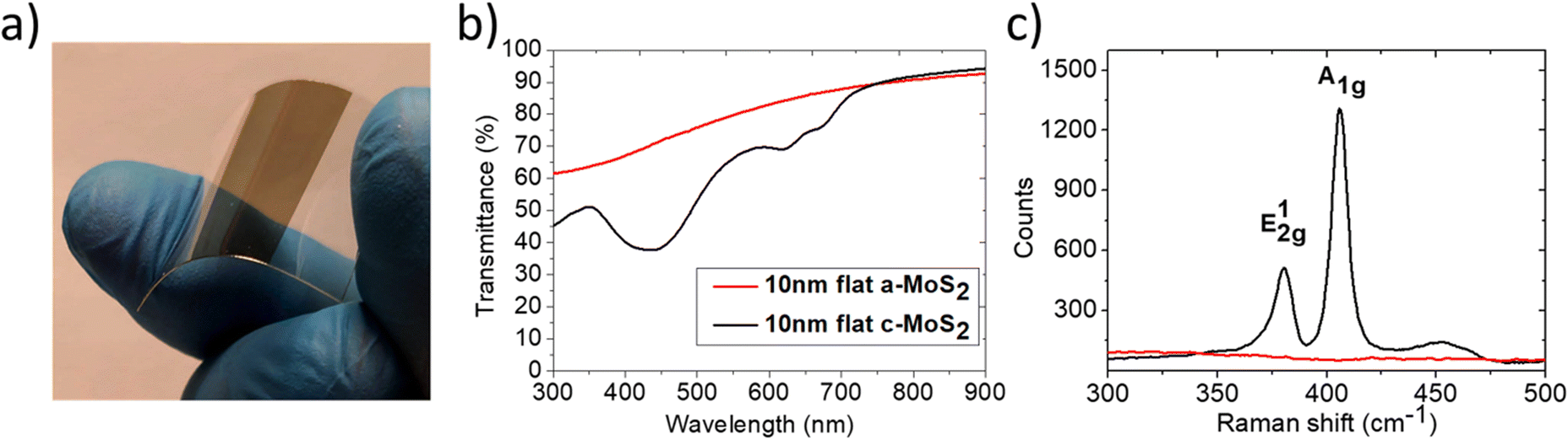 | ||
| Fig. 1 (a) Picture of a large-scale RF sputtered few-layer MoS2 film (10 nm thickness) deposited onto a flexible polymer substrate. (b) Transmission spectra of few-layer a-MoS2 (10 nm thickness – red line) and c-MoS2 (10 nm thickness – black line). (c) Raman spectra of a-MoS2 (red line) and c-MoS2 (black line). | ||
A reference a-MoS2 layer grown on a silica substrate is thermally recrystallized11 after growth, by annealing up to 750 °C within a tube furnace in the presence of sulphur vapour to preserve the stoichiometry. To confirm the effect of the recrystallization process, both the a-MoS2 and crystalline MoS2 (c-MoS2) layers, with a thickness of 10 nm, are optically characterized. The optical extinction spectra recorded over a broadband near-UV (NUV)-visible (VIS)-near-infrared (NIR) spectral range (Fig. 1b) present markedly different signatures. While in the a-MoS2 case an unstructured spectrum is detected (red trace), in the c-MoS2 case (black trace), three well defined transmission minima become evident and allow us to identify the semiconducting 2H-MoS2 phase.43 The two minima at 675 nm and 625 nm correspond to the characteristic A and B excitons, while the broader minimum detected at 400 nm is due to higher energy electronic transitions (the so called ‘band nesting’ region).44 These conclusions are independently confirmed by the micro-Raman spectra (Fig. 1c), which show the typical E12g and A1g vibrational modes excited at 380 and 406 cm−1, corresponding to the in-plane and out-of-plane Mo–S stretching modes, respectively. These typical features are only visible for the c-MoS2 film (black line). In the following, the recrystallization step to form c-MoS2 will be performed only for reference TMD films supported on thermally stable silica substrates, while the remaining part of the experimental observation will be performed on a-MoS2 films as they can be supported by soda lime glass and polymeric substrates, which do not tolerate thermal annealing.
The optical transmittance through the c-MoS2 film amounts to a value as high as 65% at 675 nm wavelength, corresponding to the A exciton, while above 780 nm, the optical transmittance of the sub-bandgap photons (i.e. energy below 1.55 eV) exceeds 90%. It is thus clear that effective solutions must be adopted to substantially increase the light harvesting properties of 2D-TMD semiconductor films if one is aiming at real world photoconversion applications.
In order to enhance the light matter interaction within the ultra-thin MoS2 layers, we adopted an original approach based on flat-optics to redirect the light wavefront parallel to the active layer reshaped to form an anisotropic and periodic nanogrooved medium. The ultra-thin a-MoS2 layer was conformally deposited on top of a polymer nanostructured template (as sketched in Fig. 2a), thus forming a periodic subwavelength grating that is capable of exciting lattice resonances.
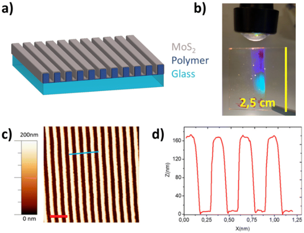 | ||
| Fig. 2 (a) Sketch of the sample analysed, which is composed of an ultra-thin layer of MoS2 deposited conformally on a polymeric grating on a glass substrate. (b) Photo of the diffraction effect induced by the periodic grating (the yellow scale bar represents 2.5 cm). (c) AFM topography of a bare polymeric template. The red scale bar represents 800 nm. (d) Extracted AFM line profile corresponding to the blue line in panel (c). | ||
These templates were nanofabricated using laser interference lithography (LIL), discussed in more detail in the Methods section. The optical interference fringes are impressed onto a transparent polymeric thin film coating that can be supported both on a rigid glass substrate as well as on a flexible polymer (such as polycarbonate). The periodic nanogrooves extend over large areas, at the cm2 scale, and contribute to steering propagation of the light wavefront, as clearly shown in Fig. 2b. The interference conditions were chosen to form a periodic array of anisotropic nanostructures characterized by a height of (160 ± 10) nm and by a subwavelength periodicity of (296 ± 10) nm, as highlighted by the AFM image and by the cross-section profile (Fig. 2c and d, respectively) and by the autocorrelation map (Fig. SI1†).
On top of the nanogrooved polymer template we conformally deposited a large-area 30 nm thick a-MoS2 layer, obtained by physical ion beam sputtering of a stoichiometric MoS2 target. Thanks to the high optical density of the 2D-TMD layer, the nanorippled film acquires flat-optic functionality, boosting light–matter interaction and photo-conversion efficiency even at the limit of ultrathin films, as revealed by the optical extinction spectra shown in Fig. 3b.
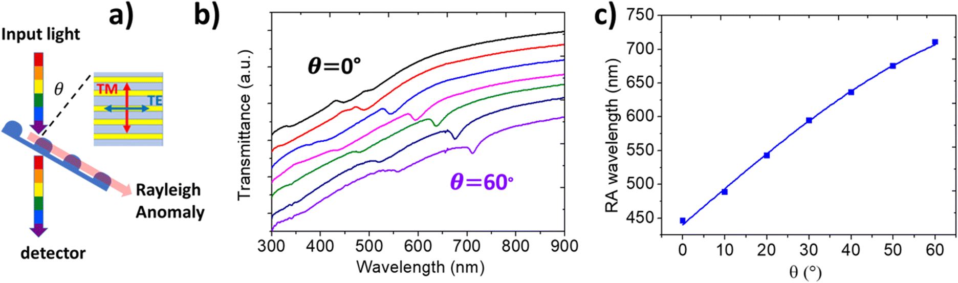 | ||
| Fig. 3 (a) Schematic of the optical configuration adopted for the angle-resolved extinction measurements. The incident light is linearly polarized perpendicular to the incidence plane and parallel to the grating long axis (TE polarization). (b) Experimental angle-resolved transmission spectra measured upon increasing incidence θ from 0° (black curve) to 60° (purple curve). A relative offset of 10% has been introduced from one spectrum to the next for better reading. The red/blue squares highlight the RA modes corresponding to the external/internal interface. (c) Position of the RA minima corresponding to the external (red dots) and to the internal (blue squares) interface, measured for different angles. Solid curves represent the theoretical position of the RA (red and blue curves), obtained from eqn (1). | ||
We detected the optical response using angle-resolved NUV-VIS-NIR extinction spectroscopy. The sample was illuminated by a linearly polarized collimated beam (diameter ≈ 2 mm) at a given incidence angle θ with respect to the surface normal (as shown by the sketch in Fig. 3a), with the electric field oriented perpendicular to the incidence plane and parallel to the elongation axis of the periodic nanostructures (s-TE polarization). The extinction spectra detected at different light incidence angles (θ), shown in Fig. 3b with a relative offset for the sake of clarity, clearly underline the presence of a dispersive optical mode that red-shifts with increasing light incidence angle (blue bars). The dominant extinction mode coherently shifts from 450 nm to 720 nm as θ increases from 0° (black curve) to 60° (violet curve). In the extinction spectra of Fig. 3b, a second weaker feature (red bars), blueshifted by about 150 nm, is also visible. Such optical features of the periodic a-MoS2 array are attributed to evanescent Rayleigh anomalies (RAs), which resonantly redirect the light flow parallel to the periodically corrugated MoS2 interface, either at the air or at the substrate side, thus coupling efficiently the incident light to the thin TMD layers. In this way, it is possible to both increase light scattering45 and induce a strong in-plane light deflection and confinement in the active layer.
As a result, photon absorption is enhanced in the 2D-TMD material itself boosting the photogeneration of electron–hole pairs, and at the same time strong electromagnetic confinement is induced in proximity of the few-layer MoS2 lattice. To confirm the attribution of the optical modes to the Rayleigh anomalies, we consider their characteristic dispersion described by the following equation:46,47
mλm = D(nf ± n0![[thin space (1/6-em)]](https://www.rsc.org/images/entities/char_2009.gif) sin(θ)) sin(θ)) | (1) |
As highlighted in Fig. 3c, the detected dispersion of the transmission dips corresponding to the RA modes at the external/internal interface (red/blue squares, respectively), in good agreement with the model described in eqn (1), in which the only free parameter is the effective refractive index nf. In the model, we fix the value of n0 equal to 1 (corresponding to air) and the first order m = 1, and a value of the periodicity D = 290 ± 10 nm compatible with the AFM images is assumed. The blue and red lines represent eqn (1), respectively assuming nf,ext = 1.55 ± 0.03 and nf,int = 1.05 ± 0.03. Such effective index values are compatible with an effective medium formed at the inner interface between MoS2 and silica, and at the outer interface with air. Such results also demonstrate a capability to tune the spectral position of the RA modes within the VIS spectral range, enabling a fine tuning of the photon harvesting properties by simply controlling the illumination geometry or the TMD nanoarray periodicity.
A direct demonstration of the light harvesting enhancement in the nanorippled MoS2 film can be provided by measuring the photobleaching rate of molecular dye probes such as MB in proximity to the MoS2 surface. This photochemical reaction is of great interest for waste-water remediation as MB is a polluting molecule widely used in the textile sector. In a first experiment, we checked the photocatalytic properties of 10 nm thick MoS2 films deposited via PVD on flat substrates. We compared the MB photobleaching rate on as-deposited a-MoS2 films and on recrystallized c-MoS2 films.
The photocatalytic properties of both samples were measured using a custom developed setup that allows us to illuminate the 2D-TMD layers, immersed in the MB solution, at variable angles, as sketched in Fig. 4a.
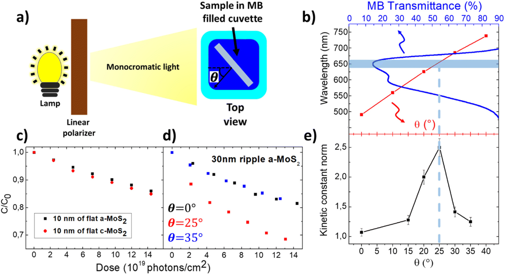 | ||
| Fig. 4 (a) Top view sketch of the experimental setup (more details are provided in the Methods and Fig. SI3b†). (b) Transmission spectra of the MB solution at normal incidence (blue line, top axis) compared with the resonant wavelength of the RA detected in water at variable θ (red squares, bottom axis). The light blue band represents the wavelength of the nearly monochromatic illumination beam employed in the photodissociation experiments. (c) Normalized concentration of the MB solution containing a sample with 10 nm of a-MoS2 (black squares) and the solution containing a sample with 10 nm of c-MoS2 (red circles) as a function of photon dose (pump source wavelength λ = 660 nm). (d) Normalized concentration evolution of the MB solution containing a 30 nm thick rippled film of a-MoS2 at θ = 0° (black squares), θ = 35° (blue squares) and θ = 25° (red squares) plotted as a function of photon fluence (pump source wavelength λ = 660 nm). For the concentration values shown in panels (c and d), the relative error on the measurement is 1%. (e) Plot of the kinetic constant of the photo-bleaching reaction detected for different light incidence angles θ. The red line at θ = 25° highlights that the RA is resonantly excited under the narrowband illumination conditions. | ||
For this purpose, we fabricated by 3D printing a miniaturized rotatable sample holder fitted to the quartz cuvette (details provided in Methods and in Fig. SI3b†). The sample, placed inside a quartz cuvette filled with a MB solution (initial concentration C0 = 1.3 × 10⁻⁵ mol L−1), was illuminated by a monochromatized and linearly polarized xenon lamp source. In this way, the sample could be oriented at variable angles θ with respect to the light beam, as revealed in the photograph of Fig. SI3b.† The samples were excited with a narrowband light beam at 660 ± 25 nm wavelength, resonant with the maximum of MB absorbance (Fig. 4b) and very close to the A excitonic mode of the ultra-thin c-MoS2 shown in Fig. 1b. The illumination source was kept at an irradiance of 2 mW cm−2, as measured on the cuvette surface, which corresponds to a spectral irradiance reduced by a factor of 10 with respect to the AM 1.5G reference solar irradiance spectrum. The concentration of the MB solution, C, was monitored during the exposure at regular time intervals by measuring the optical extinction through the solution with a fiber coupled optical transmission setup (for more details, see Methods).
In Fig. 4c, the evolution of the concentration C of the MB solution, normalized to the initial value C0, in the presence of 10 nm thick c-MoS2 (red dots) and a-MoS2 (black squares) films, is plotted as a function of the photon dose incident to the reference flat films. For both the exposures, the samples were kept at normal incidence with respect to the illumination beam. The plot qualitatively evidences that the MB photobleaching rate is almost equivalent in the two cases.
In order to compare more quantitatively the photocatalytic activity of the samples, we calculated the kinetic constant k according to the first order reaction kinetic law [C] = [C0]e−kt where C is the MB concentration as a function of time t and C0 is the concentration of MB at the beginning of the exposure. Due to the low photon doses used, the exponential law can be approximated to first order by a linear law: [C] = [C0](1 − kt). In the case where sample illumination was performed under non-normal incidence conditions, the rate k was corrected by a factor 1/cos(θ) to consider the reduced photon flux. For the two experiments of Fig. 4c, almost equivalent rates kc-MoS2 = 0.030 ± 0.002 h−1 and ka-MoS2 = 0.026 ± 0.002 h−1 were found. For both samples, the photodissociation rate is higher than that of the bare MB solution illuminated at 660 nm, which is kbare_MB = 0.020 ± 0.001 h−1. This result highlights the intrinsic photocatalytic properties of both the c-MoS2 and a-MoS2 flat reference films.
Since the difference in photobleaching rate between the two reference films is almost negligible, in the following we will focus on the study of the photocatalytic performance of the a-MoS2 films. These are indeed particularly attractive in view of real-word water remediation applications based on 2D-TMDs because their growth occurs at room-temperature and is compatible with low cost and large area flexible templates, which would not withstand a high temperature recrystallization process.
After observing the photocatalytic properties of the planar a-MoS2 film, in a second set of observations, we thus aimed to maximize the photochemical reactivity by exploiting the flat-optic photon harvesting configuration sketched in Fig. 2a. In Fig. 4d, we show the reactivity of a nanogrooved 30 nm thick a-MoS2 film for different illumination angles θ (0°, 25° and 35°) by plotting the evolution of the concentration C of the MB solution, normalized to the initial value C0, as a function of photon dose at a fixed illumination wavelength λ = 660 nm. At normal incidence (θ = 0°, black squares), we observe a slight enhancement of the reaction kinetic constant for the nanopatterned sample with respect to the reference flat sample, k0° = 0.038 ± 0.002 h−1. This is attributed to the increased MoS2 thickness, and to the larger effective surface area of the nanogrooved sample, estimated by AFM line profiles to be 1.5 times higher than that of the reference flat sample. Remarkably, the reaction kinetic constant is sharply boosted when the nanopatterned sample is illuminated at an angle θ = 25° (red squares) at which the RA, measured in water (more details are provided in SI2†), is resonant with the illumination (Fig. 4b). In this case, we observe k25° = 0.089 ± 0.005 h−1. For this condition, the kinetic constant is 2.3 times larger than that of the same sample illuminated at normal incidence and 3.4 times that of the reference flat sample. A further increase of the illumination angle to θ = 35° (black squares) detunes the RA and the reaction kinetic constant drops down to k35° = 0.044 ± 0.003 h−1. This observation was confirmed in an additional set of experiments in which the illumination angle θ was varied systematically, while leaving the illumination wavelength constant at 660 nm, in correspondence to the maximum absorption of the MB solution (Fig. 4b). Each of these experiments at variable angles was analysed using the first order kinetic model, determining the kinetic constant normalised to the value k0° measured for normal incidence illumination. In Fig. 4e, we summarise the result of such experiments, finding a remarkable dependence of photobleaching rate on the illumination angle, leading to a sharp maximum at θ = 25° (Fig. 4b). Under these conditions, the kinetic photobleaching constant is amplified by a factor of 2.3 with respect to the non-resonant conditions found for non-optimised illumination at normal incidence, as shown before.
This result is attributed to the flat optics functionalization of the surface and, more specifically, to the ability to modify the spectral match of the inner RA with the chosen illumination wavelength at 660 nm and with the maximum of molecular absorbance (Fig. 4b). Under such optimised illumination conditions, the incident light beam is redirected by the photonic anomaly to flow parallel to the surface, thus enabling both a local enhancement of the electromagnetic field in the near-surface region and increased absorption in the active TMD semiconductor film. Both these features contribute to the photobleaching of dye molecules,48 as recently demonstrated in the case of plasmonic nanoarrays. In the present case, the absorption enhancement is linked to the photogeneration of excited carriers and excitons in the TMD film, which play an important role in the photobleaching process.
In order to evaluate in a direct way the relevance of the absorption channel in the nanogrooved TMD sample, we analysed the total absorption in a custom modified integrating sphere set-up, which allows us to insert the sample inside the sphere with a controlled illumination angle θ in s-TE polarization (more details are provided in Methods and in Fig. SI5†). Specifically, thanks to another 3D printed miniaturized rotating sample holder attached to the integrating sphere, the optical setup allows us to detect the signal T(θ) due to the sum of direct transmission, diffused forward/backward and specular reflection at a specific illumination angle θ. Optical absorption from the sample is then defined in a straightforward way as A(θ) = 1 − T(θ).
In Fig. 5a, the absorption spectra for different illumination angles of 30 nm thick flat reference MoS2 (dashed lines) and 30 nm thick nanorippled MoS2 (continuous lines) are reported. For all the spectra corresponding to the nanorippled sample, a broadband and omnidirectional enhancement of absorption is visible. The latter can be attributed to an increase of light scattering in the Mie regime, effectively promoted by the high index 2D-TMD nanostructures,49 and to waveguiding and trapping in the supporting dielectric substrate. In addition, for the spectra acquired under tilted illumination conditions, a further resonant and dispersive absorption band is visible, whose spectral position red shifts with increasing illumination angle, in good agreement with the extinction feature corresponding to the RA optical anomalies (Fig. 3b and c). To better analyse the absorption gain, in Fig. 5b, we report the ratio between the absorption spectra of the nanostructured sample and the flat sample. From these spectra, it is clear that the absorption of the sample more than doubled in a broadband region corresponding to a spectral range from 500 nm (lower limit of the supercontinuum laser employed for illumination) to 800 nm (onset of MoS2 absorption corresponding to the A exciton transition – see Fig. 1b). Moreover, for the tilted samples, a sharp resonant enhancement of absorption is visible and reaches up to 300% corresponding to the inner RAs confined at the buried MoS2 interface, observed in the transmission spectra (Fig. 3b). The presence of the absorption gain in the nanostructured MoS2 films is evidence that the MoS2 photogenerated carriers may play a role in the previously observed increased rate of MB photobleaching. As expected, the outer RAs that predominantly concentrate the electromagnetic field at the air interface contribute in a limited way to the optical absorption gain in MoS2, as reported in Fig. 5b.
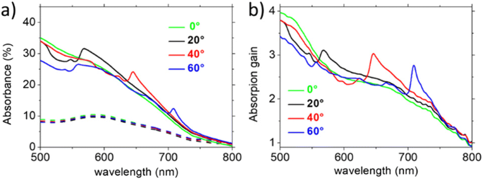 | ||
| Fig. 5 (a) Optical absorption spectra extracted from an integrating sphere set-up recorded under different incidence angle illumination conditions and TE polarization of the incident light. The dashed lines correspond to a 30 nm flat MoS2 film while the continuous lines correspond to a 30 nm rippled MoS2 film. (b) Absorption gain at different illumination angles defined as the ratio between the absorption spectra of the nanostructured sample and the flat sample. | ||
Conclusions
We demonstrate the capability to achieve shape engineering of ultra-thin TMD layers conformally grown on top of large-scale periodic nanogrooved templates, featuring flat-optic functionalities. The hybrid polymeric/MoS2 interface enables manipulation of the optical wavefront, redirecting it parallel to the active interface when the RAs are resonantly excited with a narrowband illumination beam, thus promoting photon harvesting and enhanced photobleaching of polluting dye probes.We employed a LIL approach to fabricate homogenous patterned large area samples (cm2 scale) as subwavelength periodic nanogratings. These lattices are able to support the conformal growth of ultra-thin films of a-MoS2 precisely following the nanogrooves. For the deposition, we employed a PVD method that is compatible with large area and scalable processes and, in addition, can be used with flexible polymeric samples. The nanogrooved a-MoS2 layers support photonic anomalies that can be tailored across the VIS-NIR region from 450 nm to 720 nm by simply optimizing the illumination angle.
We demonstrate the optimal photon harvesting properties of nanogrooved few-layer a-MoS2 by using these templates in a standard photobleaching reaction of polluting MB dye. We performed experiments at fixed wavelength of the light source, while modifying the incidence angle on the sample. The narrowband excitation of the RA tuned in resonance to the molecular absorption strongly boosts the photochemical properties of the solution, giving rise to a clear maximum of the photobleaching kinetic constant. This behaviour arises due to the enhanced light–matter interaction promoted by the RA mode that can strongly confine the light within the ultra-thin re-shaped MoS2 layer. The resonant RA excitation induces both an enhancement of the photon absorption, with higher carrier photogeneration within the active layer, and an amplified local field with boosted reactivity at the surface. The enhanced photobleaching of MB demonstrates the efficiency of this light trapping solution for photon harvesting and photo-conversion in ultra-thin TMD layers.
These results thus qualify the large area hybrid 2D-TMD/polymer layers as promising candidates for cost-effective photocatalytic waste-water remediation applications. Additionally, this flat-optics approach is very promising for promoting efficient light trapping in ultra-thin semiconductor layers for wider applications in optoelectronics, photonics, and quantum technologies.
Methods
Sample fabrication
The growth of large-area MoS2 rippled films supported on glass substrates was achieved by a Laser Interference Lithography (LIL) technique combined with the deposition of a thin film of a-MoS2. In particular, the following fabrication steps were performed (see Fig. SI4†): (A) spin coating of a bare glass substrate with a thin layer of a diluted positive photoresist (AZ 701 MIR thinned with AZ EBR solvent). (B) Impression of the polymeric film with our customized LIL setup in the Lloyd configuration and its development. Specifically during the exposure, the optical interference fringe pattern is impressed onto the polymer, then it is developed with a developer (AZ MIF) to obtain a large-area pattern of laterally separated polymer stripes (AFM image and line profile are shown in Fig. 2c and d). The parameters used for the LIL technique were optimized to obtain a pattern of polymer resist stripes with a periodicity P = 300 nm. (C) Deposition of a thin MoS2 film on the polymeric mask using RF sputtering at normal incidence.The MoS2 film was deposited by a custom RF sputtering system using a 2′′ MoS2 target. During the experiment, we used an argon atmosphere; the base pression of the chamber was 2 × 10⁻⁶ mbar and it reached 6 × 10⁻² mbar with injection of the argon during the MoS2 deposition. During the deposition, the power applied to the target was 8 W and the thickness was monitored using a calibrated quartz microbalance.
Morphological characterization
Atomic force microscopy topographies of the nanogrooved surface were acquired by means of a Nanosurf S Mobile microscope operating in non-contact mode. The analysis of AFM images was performed with WsXM software50 both in terms of direct topography and of self-correlation maps (Fig. SI1†). The sample topographies were analysed at multiple locations separated by macroscopic distances.Optical characterization
Normal incidence extinction spectra of the nanogrooved sample and MB solutions were acquired in the 300–1100 nm spectral range by coupling with a fiber a compensated halogen–deuterium lamp (DH-2000-BAL, Mikropak) to a Vis-NIR spectrometer (HR4000, Oceans Optics). The spot size was macroscopic with a diameter of about 2 mm. For linearly polarized measurements, a Thorlabs Glen-Thompson polarizer was used. Flat bare glass was used as a reference in the case of the nanogrooved sample measurements performed in air. An empty cuvette was used as the reference in the case of MB solution measurements.For the angle resolved transmission measurement, a custom-made system was used (SI3†). That apparatus used the same lamp and spectrometer as those of the system presented before and it allowed us to record angle resolved spectra in air and in liquids.
Angle resolved total absorption measurements
A custom-modified optical setup based on a Thorlabs 4P4 integrating sphere was developed (Fig. SI5†). A polarized supercontinuum light source (SuperK COMPACT – NKT Photonics) was coupled in free space to the integrating sphere via polarizers and broadband neutral filters. The samples were introduced into the integrating sphere via a custom-developed rotating sample holder that allows us to control the incidence angle of the illumination source. This holder was 3D printed using a white PLA filament. It is thus possible to control the light incidence angle (θ) on the sample, while the outcoming light is coupled to a VIS-NIR optical spectrometer (Ocean Optics HR4000) via an optical fiber.Photocatalysis experiments
The MB concentration was kept constant during the various experiments at about 1.3 × 10⁻⁵ mol L−1 by diluting MB powder in MQ water. The concentration of the MB solution was estimated by measurement of the solution absorbance (A = −log(T), where T is the transmittance) and using the Beer Lambert law resolved for the concentration C = Ad−1ε−1, where d is the optical path expressed in cm and ε is the molar absorption coefficient, for which we used the literature value of 7.5 × 10⁵ L mol−1 cm−1. Two quartz cuvettes with a 1 cm side square internal section were filled with 2 mL of MB solution and a little magnetic stirrer. The cuvette top was covered with parafilm to minimize evaporation of the solvent. Then, the cuvettes were left to stir at room temperature for 1 h. The sample was then put inside one of the cuvettes equipped with a custom 3D-printed sample holder that allows us to rotate the sample inside the cuvette and to perform illumination at a specific angle θ (see diagrams and photograph in Fig. 4a and Fig. SI3b†). Both MB solutions were left to stir for another hour to reach a complete surface absorption/desorption equilibrium before exposure.After this initial procedure, both cuvettes were exposed to a tunable light source (Newport TLS130B-300X) equipped with a 300 W xenon arc lamp, a CS130B monochromator and a 1-inch output flange. The monochromatized beam (±25 nm bandwidth) passes through a wire grid polarizer (Thorlabs WP25M-UB) before reaching the cuvettes, so that the electrical component of the electromagnetic radiation oscillates parallel to the MoS2 nanostripes. To illuminate uniformly both the cuvettes, they were placed 40 cm from the lamp output flange.
With a Newport 818-UV optical power detector connected to a Newport 1919-R optical power meter, we measured the average beam power density hitting the surface of the cuvettes. The source power was set in order to have a power density equal to 2 mW cm−2 for all the experiments performed. To even out the exposure of the cuvettes, they were swapped every 30 min. At regular intervals of photon exposure, the absorbance of both solutions was measured using the extinction set-up described previously and a custom-made cuvette holder. The absorbance evolution of the MB solution containing the sample with a variable angle of incidence with respect to the illumination is discussed and compared in the Results and discussion section.
Author contributions
G. F. fabricated samples, performed photodissociation experiments and drafted the original manuscript. M. G. developed and optimised the 2D-TMD deposition process. G. Z. developed the optical absorption setup. D. C. developed and optimized the lithographic templates. M. B. developed the photodissociation setup and protocol. M. C. G. and F. B. d. M. conceptualized the activity, acquired funding, and undertook project supervision. All authors contributed to manuscript review and editing.Conflicts of interest
The authors declare no conflict of interest.Acknowledgements
F. B. d. M. and M. C. G. acknowledge financial support provided by Ministero dell'Università e della Ricerca, within the project “Dipartimento di Eccellenza 2018–2022” art. 1, c. 314-337, Legge 232/2016. M. C. G. acknowledges financial support provided by Ministero degli Affari Esteri e della Cooperazione Internazionale within the bilateral project Italy–Vietnam 2021–2023 “Large-area 2D/plasmonic heterostructures for photocatalysis and energy storage (H2D)”. F.B.d.M and D.C. acknowledge support by Regione Liguria for support within the PO FSE Regione Liguria 2014-2020. F. B. d. M. and M. C. G. acknowledge support by Università degli Studi di Genova within the project “Fondi di Ricerca di Ateneo” and BIPE2020. F.B.d.M and D.C. acknowledge ICTP, Trieste, Italy, for the TRIL Fellowship.Notes and references
- K. F. Mak and J. Shan, Nat. Photonics, 2016, 10, 216–226 CrossRef CAS.
- H. H. Huang, X. Fan, D. J. Singh and W. T. Zheng, Nanoscale, 2020, 12, 1247–1268 RSC.
- X. Zhang, Z. Lai, Q. Ma and H. Zhang, Chem. Soc. Rev., 2018, 47, 3301–3338 RSC.
- S. Li, Y.-C. Lin, X.-Y. Liu, Z. Hu, J. Wu, H. Nakajima, S. Liu, T. Okazaki, W. Chen, T. Minari, Y. Sakuma, K. Tsukagoshi, K. Suenaga, T. Taniguchi and M. Osada, Nanoscale, 2019, 11, 16122–16129 RSC.
- K. Wang, J. Wang, J. Fan, M. Lotya, A. O'Neill, D. Fox, Y. Feng, X. Zhang, B. Jiang, Q. Zhao, H. Zhang, J. N. Coleman, L. Zhang and W. J. Blau, ACS Nano, 2013, 7, 9260–9267 CrossRef CAS PubMed.
- A. Castellanos-Gomez, R. Roldán, E. Cappelluti, M. Buscema, F. Guinea, H. S. J. van der Zant and G. A. Steele, Nano Lett., 2013, 13, 5361–5366 CrossRef CAS PubMed.
- N. Huo, S. Gupta and G. Konstantatos, Adv. Mater., 2017, 29, 1606576 CrossRef PubMed.
- D. Maeso, A. Castellanos-Gomez, N. Agraït and G. Rubio-Bollinger, Adv. Electron. Mater., 2019, 5, 1900141 CrossRef.
- C. Trovatello, H. P. C. Miranda, A. Molina-Sánchez, R. Borrego-Varillas, C. Manzoni, L. Moretti, L. Ganzer, M. Maiuri, J. Wang, D. Dumcenco, A. Kis, L. Wirtz, A. Marini, G. Soavi, A. C. Ferrari, G. Cerullo, D. Sangalli and S. D. Conte, ACS Nano, 2020, 14, 5700–5710 CrossRef CAS PubMed.
- J. van de Groep, J.-H. Song, U. Celano, Q. Li, P. G. Kik and M. L. Brongersma, Nat. Photonics, 2020, 14, 426–430 CrossRef CAS.
- C. Martella, C. Mennucci, A. Lamperti, E. Cappelluti, F. B. de Mongeot and A. Molle, Adv. Mater., 2018, 30, 1–9 CrossRef PubMed.
- X. Cao, C. Tan, X. Zhang, W. Zhao and H. Zhang, Adv. Mater., 2016, 28, 6167–6196 CrossRef CAS PubMed.
- M.-R. Gao, Y.-F. Xu, J. Jiang and S.-H. Yu, Chem. Soc. Rev., 2013, 42, 2986 RSC.
- C. Palacios-Berraquero, D. M. Kara, A. R.-P. Montblanch, M. Barbone, P. Latawiec, D. Yoon, A. K. Ott, M. Loncar, A. C. Ferrari and M. Atatüre, Nat. Commun., 2017, 8, 15093 CrossRef CAS PubMed.
- C. C. Price, N. C. Frey, D. Jariwala and V. B. Shenoy, ACS Nano, 2019, 13, 8303–8311 CrossRef CAS PubMed.
- A. Molina-Sánchez, K. Hummer and L. Wirtz, Surf. Sci. Rep., 2015, 70, 554–586 CrossRef.
- X. Bao, Q. Ou, Z. Xu, Y. Zhang, Q. Bao and H. Zhang, Adv. Mater. Technol., 2018, 3, 1800072 CrossRef.
- J. Wong, D. Jariwala, G. Tagliabue, K. Tat, A. R. Davoyan, M. C. Sherrott and H. A. Atwater, ACS Nano, 2017, 11, 7230–7240 CrossRef CAS PubMed.
- M. C. Giordano, G. Zambito, M. Gardella and F. Buatier de Mongeot, Adv. Mater. Interfaces, 2022, 2201408, DOI:10.1002/admi.202201408.
- C. Yim, M. O'Brien, N. McEvoy, S. Winters, I. Mirza, J. G. Lunney and G. S. Duesberg, Appl. Phys. Lett., 2014, 104, 103114 CrossRef.
- Z. Li, X. Meng and Z. Zhang, J. Photochem. Photobiol., C, 2018, 35, 39–55 CrossRef CAS.
- E. Parzinger, B. Miller, B. Blaschke, J. A. Garrido, J. W. Ager, A. Holleitner and U. Wurstbauer, ACS Nano, 2015, 9, 11302–11309 CrossRef CAS PubMed.
- D. Voiry, J. Yang and M. Chhowalla, Adv. Mater., 2016, 28, 6197–6206 CrossRef CAS PubMed.
- M. Deng, Z. Li, X. Rong, Y. Luo, B. Li, L. Zheng, X. Wang, F. Lin, A. J. Meixner, K. Braun, X. Zhu and Z. Fang, Small, 2020, 16, 2003539 CrossRef CAS PubMed.
- J. Lu, G. Niu, X. Ren, D. Bao, H. Chen, H. Yang, X. Lin, S. Du and H.-J. Gao, Nanoscale, 2021, 13, 19165–19171 RSC.
- Y. Fan, J. Wang and M. Zhao, Nanoscale, 2019, 11, 14836–14843 RSC.
- M. Ahmadi, O. Zabihi, S. Jeon, M. Yoonessi, A. Dasari, S. Ramakrishna and M. Naebe, J. Mater. Chem. A, 2020, 8, 845–883 RSC.
- S. Kundu and A. Patra, Chem. Rev., 2017, 117, 712–757 CrossRef CAS PubMed.
- K. Chang, Z. Mei, T. Wang, Q. Kang, S. Ouyang and J. Ye, ACS Nano, 2014, 8, 7078–7087 CrossRef CAS PubMed.
- D. Merki and X. Hu, Energy Environ. Sci., 2011, 4, 3878 RSC.
- Y. Gao, C. Chen, X. Tan, H. Xu and K. Zhu, J. Colloid Interface Sci., 2016, 476, 62–70 CrossRef CAS PubMed.
- M. Wu, L. Li, Y. Xue, G. Xu, L. Tang, N. Liu and W. Huang, Appl. Catal., B, 2018, 228, 103–112 CrossRef CAS.
- G. Tagliabue, A. S. Jermyn, R. Sundararaman, A. J. Welch, J. S. DuChene, R. Pala, A. R. Davoyan, P. Narang and H. A. Atwater, Nat. Commun., 2018, 9, 3394 CrossRef PubMed.
- H. A. Atwater and A. Polman, Nat. Mater., 2010, 9, 205–213 CrossRef CAS PubMed.
- M. W. Knight, H. Sobhani, P. Nordlander and N. J. Halas, Science, 2011, 332, 702–704 CrossRef CAS PubMed.
- N. Yu and F. Capasso, Nat. Mater., 2014, 13, 139–150 CrossRef CAS PubMed.
- M. F. Limonov, M. V. Rybin, A. N. Poddubny and Y. S. Kivshar, Nat. Photonics, 2017, 11, 543–554 CrossRef CAS.
- M. Bhatnagar, M. Gardella, M. C. Giordano, D. Chowdhury, C. Mennucci, A. Mazzanti, G. Della Valle, C. Martella, P. Tummala, A. Lamperti, A. Molle and F. Buatier De Mongeot, ACS Appl. Mater. Interfaces, 2021, 13, 13508–13516 CrossRef CAS PubMed.
- M. Bhatnagar, M. C. Giordano, C. Mennucci, D. Chowdhury, A. Mazzanti, G. Della Valle, C. Martella, P. Tummala, A. Lamperti, A. Molle and F. B. De Mongeot, Nanoscale, 2020, 12, 24385–24393 RSC.
- Y. Liu and F. Gu, Nanoscale Adv., 2021, 3, 2117–2138 RSC.
- C. Martella, C. Mennucci, E. Cinquanta, A. Lamperti, E. Cappelluti, F. Buatier de Mongeot and A. Molle, Adv. Mater., 2017, 29, 1605785 CrossRef PubMed.
- C. Mennucci, D. Chowdhury, G. Manzato, M. Barelli, R. Chittofrati, C. Martella and F. Buatier de Mongeot, Nano Res., 2021, 14, 858–867 CrossRef CAS.
- Z. He and W. Que, Appl. Mater. Today, 2016, 3, 23–56 CrossRef.
- A. Castellanos-Gomez, J. Quereda, H. P. Van Der Meulen, N. Agraït and G. Rubio-Bollinger, Nanotechnology, 2016, 27, 115705 CrossRef PubMed.
- J. Yang, Z. Wang, F. Wang, R. Xu, J. Tao, S. Zhang, Q. Qin, B. Luther-Davies, C. Jagadish, Z. Yu and Y. Lu, Light: Sci. Appl., 2016, 5, e16046 CrossRef CAS PubMed.
- S. S. Wang and R. Magnusson, Appl. Opt., 1993, 32, 2606 CrossRef CAS PubMed.
- B. Stout, Gratings: Theory and Numeric Applications, 2013 Search PubMed.
- M. Barelli, G. Ferrando, M. C. Giordano and F. Buatier de Mongeot, ACS Appl. Nano Mater., 2022, 5, 3470–3479 CrossRef CAS.
- R. Verre, D. G. Baranov, B. Munkhbat, J. Cuadra, M. Käll and T. Shegai, Nat. Nanotechnol., 2019, 14, 679–683 CrossRef CAS PubMed.
- I. Horcas, R. Fernández, J. M. Gómez-Rodríguez, J. Colchero, J. Gómez-Herrero and A. M. Baro, Rev. Sci. Instrum., 2007, 78, 013705 CrossRef CAS PubMed.
Footnotes |
| † Electronic supplementary information (ESI) available. See DOI: https://doi.org/10.1039/d2nr05004h |
| ‡ Present address: Photonic Nanomaterials Lab, Istituto Italiano di Tecnologia (IIT), 16163 Genova, Italy. |
| § Present address: Department of Physics, Bose Institute, 93/1, Acharya Prafulla Chandra Road, Kolkata 700009, India. |
| This journal is © The Royal Society of Chemistry 2023 |