
Review on recent progress in WO3-based electrochromic films: preparation methods and performance enhancement strategies
Jin You
Zheng
 a,
Qimeng
Sun
a,
Jiameizi
Cui
a,
Xiaomei
Yu
*a,
Songjie
Li
a,
Lili
Zhang
a,
Suyu
Jiang
a,
Wei
Ma
*a and
Renzhi
Ma
b
a,
Qimeng
Sun
a,
Jiameizi
Cui
a,
Xiaomei
Yu
*a,
Songjie
Li
a,
Lili
Zhang
a,
Suyu
Jiang
a,
Wei
Ma
*a and
Renzhi
Ma
b
aEngineering Research Center of Advanced Functional Material Manufacturing of Ministry of Education, School of Chemical Engineering, Zhengzhou University, Zhengzhou 450001, China. E-mail: mawei@zzu.edu.cn; yuxm@zzu.edu.cn
bInternational Center for Materials Nanoarchitectonics (MANA), National Institute for Materials Science (NIMS), Namiki 1-1, Tsukuba, Ibaraki 305-0044, Japan
First published on 9th November 2022
Abstract
Transition metal oxides have drawn tremendous interest due to their unique physical and chemical properties. As one of the most promising electrochromic (EC) materials, tungsten trioxide (WO3) has attracted great attention due to its exceptional EC characteristics. This review summarizes the background and general concept of EC devices, and key criteria for evaluation of WO3-based EC materials. Special focus is placed on preparation techniques and performance enhancement of WO3 EC films. Specifically, four methods – nanostructuring, regulating crystallinity, fabricating hybrid films, and preparing multilayer composite structures – have been developed to enhance the EC performance of WO3 films. Finally, we offer some important recommendations and perspectives on potential research directions for further study.
 Jin You Zheng | Jin You Zheng received his BS degree in Chemical Engineering and Technology (2009) from Yanbian University, China, and his MS and PhD degrees in Chemistry (2010–2018) from Sogang University, South Korea, under the guidance of Prof. Young Soo Kang. Since July 2018, he has worked in the School of Chemical Engineering at Zhengzhou University, China. His current research interest focuses on the fabrication of electro/photocatalysts for energy and environmental applications such as water splitting, CO2 reduction, electrochromic application, and pollutant degradation. |
 Qimeng Sun | Qimeng Sun received his BS degree in Chemical Engineering and Technology from Zhengzhou University, China (2021). He is currently pursuing his MS degree in Chemical Technology at Zhengzhou University under the supervision of Prof. Jin You Zheng. His research interests are mainly focused on the preparation of WO3-based transition metal oxide films by spin-coating, electrodeposition and hydrothermal methods, and the fabrication of devices for electrochromic applications. |
 Xiaomei Yu | Xiaomei Yu received her BS degree in Applied Chemistry (2011) from the Henan Institute of Science and Technology, China, and her PhD degree in Applied Chemistry (2011–2017) from Ajou University, South Korea, under the guidance of Prof. Yu Kwon Kim. Since December 2017, she has worked in the School of Chemical Engineering at Zhengzhou University, China. Her current research interest focuses on the fabrication of electro/photocatalysts for sustainable energy conversion applications. |
 Wei Ma | Wei Ma is an associate professor at the School of Chemical Engineering at Zhengzhou University. He received his bachelor's degree in Inorganic Nonmetal Material Engineering from Central South University in 2009 and obtained his Ph.D. degree in Mineral Material Science from Central South University in 2015. He studied at NIMS as a joint Ph.D. student from September 2013 to September 2015. Since 2016, he has worked for Zhengzhou University. His major work is focused on the fabrication of layered materials and electrochemistry. |
1. Introduction
As human society advances the need for energy increases, which is causing a rise in carbon dioxide emissions that results in an annual global injection of around 10 billion tons of carbon into the atmosphere.1 Buildings consume 30–40% of the world's primary energy; in absolute terms, building-related greenhouse gas emissions may be around 15.6 million metric tons of CO2 equivalents in 2030.2 The majority of this energy is used for cooling, heating, lighting, and electrical appliances, with ∼30% of it being lost via windows.3 Windows are crucial for the operation and comfort of buildings, thus the use of color-changing glass is necessary to fulfill people's growing need for environmental protection. Electrochromic windows, which can dynamically change color depending on the applied voltage to regulate visible and near-infrared radiation, are one of the solutions for lowering a building's energy loss. There is about 6.6% ultraviolet light, 44.7% visible light, and 48.7% infrared light in the solar spectrum.4 Traditional glass can only block ultraviolet light; however, electrochromic glass can dynamically modulate the intensity of the full spectrum of sunlight, such as allowing visible light to pass through while blocking infrared light, ensuring not only lighting but also heat preservation and insulation.The electrochromic device was first fabricated by Deb in 1969,5 and after that a variety of electrochromic devices (ECDs) began to be used commercially. Early ECDs were primarily utilized in electrochromic helmets and anti-glare vehicle mirrors (Fig. 1f). The application of electrochromic materials in building and transportation is therefore progressively expanding. Examples include smart windows in offices (Fig. 1a), hotels, airports, libraries, and porthole glass used in the airplane (Fig. 1d). Due to its capacity to intelligently control light intensity and temperature as well as its ability to safeguard privacy, electrochromic glass has become more popular in a variety of areas over the past few years in addition to further uses in buildings. Currently, EC smart glass is used in automobile windows, laptop and phone backs (Fig. 1e), EC displays (Fig. 1b), smart eyewear (Fig. 1c), and other products. The impact of electrochromic technology will increase with the emergence of wearable devices like VR/AR glasses, flexible electronics (like electronic skin), and flexible ECDs.
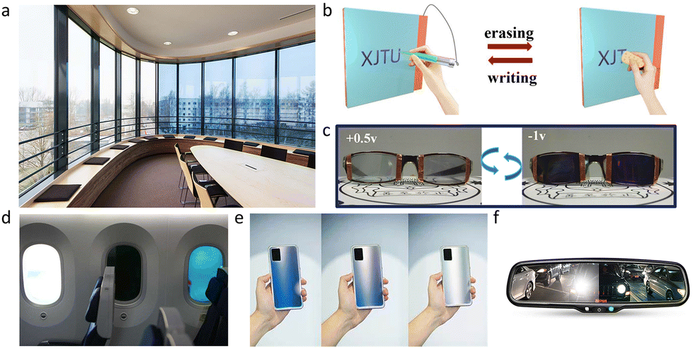 | ||
| Fig. 1 (a) An example of electrochromic windows produced by iGlass®. (b) Writing board based on electrochromism. Reproduced from ref. 13 with permission from the American Chemical Society, Copyright 2021. (c) Photographs of the electrochromic lens. Reproduced from ref. 14 with permission from the Royal Society of Chemistry, Copyright 2019. (d) Smart electrochromic aircraft windows are produced by Smart Glass VIP®. (e) Electrochromic smartphone back case produced by VIVO®. (f) Automatic dimming mirror based on electrochromism produced by Amazon®. | ||
Electrochromic materials are distinguished by their optical properties which can be reversed when an electric field is introduced. Organic small molecules such as viologens,6 conductive polymers such as PEDOT,7,8 and transition metal oxide (TMO) materials such as WO3,9 NiO,10 and V2O5,11 are the three primary types of electrochromic material. Among them, organic electrochromic materials offer faster response times and more color changes than inorganic transition metal oxides but are frequently less stable and durable, whereas TMO materials are easily processed, have good reversibility and strong electrochemical stability. Due to the injection and extraction of electrons and ions, TMO-EC materials can be modulated in the range of visible and infrared light by applying various biases.12 Researchers have thus preferred TMO materials, exemplified by WO3, due to their benefits in terms of economics and commercial potential.
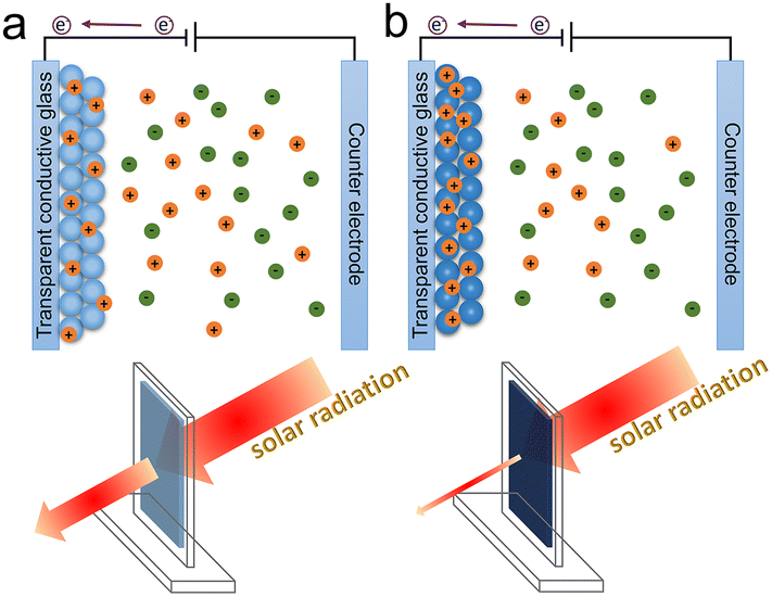
The electrochromic phenomenon of WO3 was first discovered in 1956, and electrochromism became a new development field in 1973.10 Electrochromic materials can be divided into cathodic electrochromic materials and anodic electrochromic materials based on the color-changing process, with the former coloring during cation intercalation and the latter coloring during cation extraction or anion intercalation. As a transition metal oxide, WO3 is one of the most popular cathodic electrochromic materials. The valence state of W atoms is changed when cations and charges are injected into WO3, resulting in a blue WO3 film,15 as shown in Fig. 2. The principle of electrochromic WO3 is described as follows:
| WO3(bleaching) + x(A+ + e−) ↔ AxW1−x6+Wx5+O3(coloration) | (1) |
 | ||
| Fig. 2 The electrochromic process of WO3-based film; (a) incomplete coloring state and (b) coloration state. | ||
The EC performance of WO3-based films is affected by various factors, including porosity,17 surface roughness,21,22 specific surface area,23 electrical conductivity,24 and crystallinity.25 Ion intercalation/extraction, which is the key part of the EC process, can be roughly broken down into five steps of one cycle: (1) the ions transfer from the electrolyte to the film surface; (2) the ions enter the film and move throughout the film; (3) the ions intercalate the WO3 crystal lattice; (4) the ions’ extraction from the WO3 crystal lattice; and (5) the ions move out of the film. The kinetics of the ion diffusion, insertion/extraction and charge transfer has an extreme impact on the coloring/bleaching process. The efficient strategies have been explored to improve the EC properties, such as increasing the contact area between WO3 film and electrolyte to offer more reactive sites and a short ionic diffusion path, enhancing the electrical conductivity of films to facilitate the charge transfer process, and designing specific nanostructures and composites to improve the performance.
In the past few years, nanotechnology has been verified as an extremely efficient method and widely applied in the electrochromic area. The nanostructured materials can be classified into zero-dimensional (0D, such as nanodots and nanoparticles), one-dimensional (1D, such as nanowires, nanorods, nanofibers, and nanotubes), two-dimensional (2D, such as nanosheets, nanoflakes, and nano thin-films), and three-dimensional (3D, usually some variation of special structures) materials. Designing appropriate nanostructures can strengthen the whole EC performance by regulating the morphology, porosity, surface roughness, and specific surface area of materials at the nanoscale. Meanwhile, the electrochemical and optical properties of the films are also significantly affected. In addition, combining the WO3 layer with other material layers to construct WO3-based composite structures is also an important method, which not only improves the EC properties of the composite films but also enables them with more functionality, with large electrical capacitance, high electrical conductivity and transparency. Therefore, films or ECDs based on WO3 composite structures exhibit wide application prospects.
Researchers have made great strides in the study of WO3-based EC materials, and some of these materials exhibit exceptional EC characteristics including significant optical modulation, short switching times (seconds or even sub-seconds), or high coloration efficiency (CE), as shown in Table 1. However, there are still certain difficulties and problems to be mindful of, including high costs and intricate preparation methods as well as insufficient stability. It is crucial to completely understand and overcome the related challenges to develop the technology for producing EC films on a large scale at low cost and high efficiency. Thus, more work should be done in the investigation of EC materials and devices.
| Composition and phase | Electrolyte | Preparation method | ΔT (%) | t c,90%/tb,90% (s) | CE (cm2 C−1) | Ref. |
|---|---|---|---|---|---|---|
| a, b, c and d: measured in a full device; PC: propylene carbonate; PMMA: poly (methyl methacrylate); PAAm: polyacrylamide, ACN: acetonitrile. | ||||||
| h-WO3 crystalline quantum-dots | 0.2 M LiClO4-PC | Air-brush spray-coating | 97.8 (633 nm) | 4.5/4.0 | 76.8 | 26 |
| a-WO3·H2O amorphous-quantized | 2.5 M LiClO4/PMMA | Spin coating | 70.5 (633 nm) | 2.4/0.5 | 77.0 | 27 |
| h-WO3 crystalline nanorods | 0.5 M LiClO4-PC | Hydrothermal | 52.3 (630 nm) | 1.2/1.5 | 243 | 28 a |
| WO3 crystalline nanosheets | 1 M LiClO4-PC | Casting | 62.57 (700 nm) | 10.74/6.97 | — | 29 b |
| h-WO3 crystalline coral-like nanostructure | 1 M LiClO4-PC | Hydrothermal | 78.1 (630 nm) | 5/6 | 56.5 | 30 |
| WO3 crystalline nanotree-like structure | 1 M H2SO4 | Solvothermal | 74.7 (630 nm) | 7.28/2.64 | 75.35 | 31 |
| WO3 controllable crystallinity (amorphous to crystalline) | 1 M LiClO4-PC | Magnetron sputtering | 72.5 (1000 nm) | 5.3/3.0 | 80.5 | 32 |
| WO3 amorphous/crystalline porous bilayer nanobowl | 1 M LiClO4-PC | Electrodeposition and magnetron sputtering | 93.9 (633 nm) | 3.0/3.6 | 92.3 | 33 |
| WO3 hexagonal/amorphous core/shell nanorod arrays | 1 M LiClO4-PC | Spin coating | 67.7 (800 nm) | 21/15 | 101 | 34 |
| P-doped WO3 amorphous tunneled structure | 1 M LiClO4-PC | Spin coating | 55.8 (633 nm) | 6.1/2.5 | 55.9 | 35 |
| Tb-doped WO3 amorphous porous net structure | 0.5 M H2SO4 | Hydrothermal | 66.71 (680 nm) | 9.99/3.70 | 48.33 | 36 |
| MoO3−y/WO3−x amorphous | 1 M PAAm-AlCl3 hydrogel | Spin coating | 50 (660 nm) | 4/15 | — | 13 c |
| WO3@Ag-nanowires core–shell structure | 1 M LiClO4-PC | Hydrothermal | 72 (550 nm) | 11/8 | 78.64 | 37 |
| h-WO3/TiO2 nanorods arrays | 1 M LiClO4-PC | Hydrothermal | 73.45 (633 nm) | 6.6/2.0 | 69.2 | 23 |
| WO3/PEDOT core/shell nanorod arrays | 1 M LiClO4-PC | Solvothermal and electropolymerization | 72 (633 nm) | 3.8/3.6 | 163.5 | 38 |
| WO3–MO3 triclinic columnar structure | 1 M LiClO4-PC | APCVD | 45.21 (550 nm) | — | 196.46 | 39 |
| h/o-WO3 nanoparticles | 61![[thin space (1/6-em)]](https://www.rsc.org/images/entities/char_2009.gif) :17:7:15 (ACN:PC:LiClO4:PMMA). :17:7:15 (ACN:PC:LiClO4:PMMA). |
Inkjet printing | 75.4 (633 nm) | 10/13.1 | 131.9 | 40 d |
| Porous a-WO3/Ag NFs/WO3 | 1 M LiClO4-PC | Electrodeposition | 89.7 (633 nm) | 9/19 | 58.95 | 14 |
| Nanocrystal-in-glass structure WO3 | 0.1 M LiClO4-PC | Vacuum evaporation | 92 (633 nm) | 16/11 | 61.78 | 41 |
| P8W48/W18O49 nanowires | 0.1 M LiClO4-PC | Self-assembly | 61.4 (1060 nm) | 86/78 | 121.03 | 42 |
In this review, we introduce the generic electrochromic device, its evaluation index, and several techniques for producing electrochromic films based on WO3. In addition, we review recent key strategies for enhancing electrochromic properties from four different perspectives, including nanostructuring, regulating crystallinity, fabricating hybrid films, and preparing multilayer composite structures. Also highlighted are a few potential future applications for WO3 EC films. Some potential prospects for WO3 EC films are also summarized.
2. Structure and performance evaluation of generic ECDs
2.1 Structure of generic ECDs
The structure of generic ECDs mainly consists of a 5-layer design as shown in Fig. 3.1 There are five overlapping thin layers between the two transparent substrates, including a transparent conductor layer, electrochromic film, electrolyte (ion conductor), and ion storage film or electrochromic film. The electrochromic film is the most important component of the device since it performs the function of coloring/bleaching when a suitable voltage is applied. Thus, the electrochromic performance of the entire device is mainly determined by the qualities of the electrochromic film.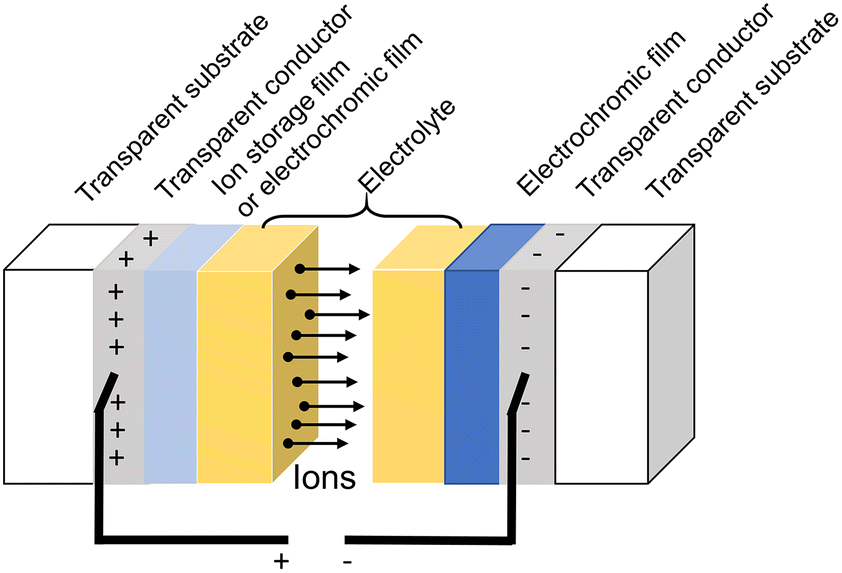 | ||
| Fig. 3 Schematic illumination of the structure of generic ECDs. | ||
Besides the electrochromic film, the electrolyte also plays an important role in providing and conducting ions, which significantly impacts on electrochromic properties of ECDs.43 The electrolyte can be categorized as liquid, gel, or solid-state, and is an ion conductor but not an electron conductor. The ion solution,16,19,44–48 ionic gel,13 and polymeric layer7,49–51 can be used as electrolytes. Among these states, liquid electrolytes have been widely used because of their high ionic conductivity, and monovalent ions such as H+, Li+, Na+, and K+ are usually used as insertion ions.16,44–49 In particular, Li+-non-aqueous solution, which has exceptional stability in the electrochemical process, is the most commonly used electrolyte for ECDs as shown in Table 1. For the monovalent ions, several disadvantages such as the corrosiveness of acid, the high cost and hazardous nature of Li+-based salt, and the large ion radius of Na+ and K+ are the limitations for wide application for ECDs. Therefore, many researchers have attempted to replace them with other ions such as Al3+, Zn2+, Mg2+,13,19,26,52–54 or some organic electrolyte.55 Al3+ is the third most abundant element on the Earth and has high electrical conductivity. Besides, the radius of Al3+ (0.054 nm) is smaller than Li+ (0.076 nm) and Na+ (0.102 nm), which is appropriate for the intercalated/de-intercalated process, and it displays higher activity in the process of intercalation.20 Obviously, one-third of the number of Al3+ provides the same amount of charge as the monovalent ion, which means the coloration/discoloration cycle is completed with fewer ions involved in the intercalated/de-intercalated process. Therefore, the long-term stability and switching time of ECDs can be improved by Al3+. However, severe limitations for Al3+ are also found, such as the strong electrostatic interactions between ions and intercalation framework, which result in difficult intercalation, and only specific WO3 nanostructures are suitable for Al3+.20 In addition, highly effective solid electrolytes have attracted much attention in recent years, due to the advantages of low cost, ease of processability, wide feasibility and high security.50 Compared with liquid or gel electrolytes, solid electrolytes are promising candidates for the development of the next generation of ECDs, since they can overcome the drawbacks of peripheral leakage and non-ideal long-term stability.
Glass is the most typical substrate material. Indium tin oxide (ITO) or fluorine-doped indium tin oxide (FTO) is frequently used as the transparent conductor material. In addition, flexible materials like polyethylene terephthalate (PET) are a possibility for creating flexible electrochromic devices. Moreover, certain nanomaterials can serve as electrical conductors. Ion storage films generally show low electron and ion resistance to achieve a rapid switching time. As a result, storage films store ions while maintaining a balanced electric charge. Finally, electrochromic films with a complementary color effect are another option for ion storage films, such as WO3-NiO.56
2.2 Performance evaluation of ECDs
To promote more applications and industrialization of ECDs, current researchers are devoted to developing different new ECDs with excellent performance parameters in various aspects. In addition, ECDs with different performance parameters are required to meet different applications; for example, smart glasses and windows with the ability to dynamically change color require high optical modulation, while flexible displays tend to need outstanding response speed. In this section, the important parameters that are used to evaluate the electrochromic performance of ECDs are demonstrated systematically.| ΔT = Tb − Tc | (2) |
| CR = Tc/Tb | (3) |
| v = ΔT/t | (4) |
| CE(λ) = ΔOD/Qd = log(Tb/Tc)/Qd | (5) |
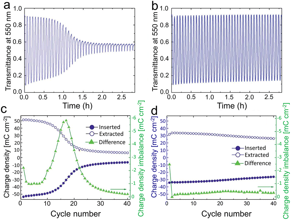 | ||
| Fig. 4 Optical data for WO3 film immersed in LiClO4-PC. (a) Transmission and durability of WO3 films at 550 nm without electrochemical pretreatment; (b) the performance for the films that have been potentiostatically pretreated at 6.0 V vs. Li/Li+ for 24 h. (c) and (d) Inserted and extracted charge density of WO3 film in CV process before and after being potentiostatically pretreated. Reproduced from ref. 59 with permission from the Royal Society of Chemistry, Copyright 2019. | ||
3. Overview of WO3 EC material
The structure of pure WO3 is the corner-sharing octahedra, in which a tungsten atom is placed in the center of each octahedron and surrounded by six oxygen atoms. This is a benign structure because spaces in the octahedral structure are large enough to allow diffusion and embedding of electrolyte ions. In recent years, WO3-based electrochromic materials have been extensively investigated as the most promising cathodic oxide due to their good EC performance and wide application fields. In addition, most of the methods used for film fabrication can be used to prepare WO3 EC films, such as electrodeposition,62,63 hydrothermal,30 magnetron sputtering,24 spray-coating,64 sol–gel,18,65etc. The EC performance of WO3 film strongly depends on its architecture, surface morphology, crystallinity, and composition. Therefore, metal doping, nanostructure, and composite design have often been used by researchers as effective strategies for improving EC performance.3.1 Fabrication methods for WO3 EC films
There are various kinds of methods to fabricate WO3 EC films, such as magnetron sputtering,56,66–72 sol–gel,49,51,73–83 hydrothermal,37,84–87 electrodeposition,14,88–91 inkjet printing,92 self-assembly,42,93,94 chemical vapor deposition (CVD),95,96 vacuum evaporation,53,97–102 and so on. The structure and EC performance of the WO3 films have obvious differences resulting from the various preparation methods and conditions. In addition, different crystallinity, being bound to the substrate tightly or not, and the density also affect the performance and service life of films. From a commercialization point of view, suitable preparation methods with the properties of low cost and high efficiency are of great value.Among these methods, magnetron sputtering can be used to fabricate a compact film. It is a kind of physical vapor deposition with the principle of using ionized high-energy noble gas ions (such as Ar+) to bombard the reactants under the action of an electric field force so that the reactants are sputtered onto the substrate in the form of molecules and atoms to form a film.103 This method can be used to fabricate films at low temperatures, and forms good bonding between the film and the substrate. However, this method has some inevitable disadvantages, such as the need for complex sputtering equipment, high cost, defects in the prepared films, etc. In addition, the switching time of the prepared films is usually not short enough to meet the requirement of ECDs. Pan et al.66 fabricated WO3 thin films through the direct current (DC) reactive magnetron sputtering method at different pressures, and a possible kinetic model of WO3 film growth was presented. The results showed that WO3 thin films have amorphous structures at different working pressures. In addition, loose and porous films that demonstrated good EC properties and stability could be obtained under high working pressure. Najafi-Ashtiani et al.104 prepared a trilayer (WO3/Ag/WO3) bi-function EC device by the high-power impulse magnetron sputtering method. The WO3 layer was deposited under an atmosphere of ultrahigh purity (99.9995%) O2 and Ar with different flow rate ratios, while the gas pressure was 2.8 mTorr. The trilayer structure exhibited low sheet resistance (23 Ω cm−2) and excellent EC performance (ΔOD = 34.5%, 30.5 cm2 C−1, tc = 22.4 s and tb = 15.0 s).
Vacuum evaporation refers to the coating materials that have been evaporated by a kind of heating evaporation method (ohmic heating evaporation, electron beam heating evaporation, arc heating evaporation, laser heating evaporation) under the vacuum condition, and then the particles fly to the surface of the substrate to condense into a film.105 This method is another physical vapor deposition method that was used early and widely. Its benefits include ease of film formation, excellent film purity, and adjustable crystallinity and microstructure. However, this method also has several disadvantages. The prepared film is easily absorbed by residual water vapor. There is inadequate adhesion between the film and substrate, and the surface of the film is not flat enough. Wang et al.98 prepared a WO3 thin film by the electron beam evaporation method on ITO glass. The deposition rate was 0.10–0.20 nm s−1 with an electron beam of 10 kV, and the thickness of the film was ca. 300 nm. The ECDs based on WO3 and Prussian blue (PB) films have good electrochemical stability and EC properties. Qiu et al.41 deposited nanocrystal-in-glass (nanocrystals embedded amorphous matrix) WO3via an electron beam evaporation method at different temperatures (room temperature to 250 °C). Pure WO3 particles with a diameter of ∼3 mm were bombarded by an electron beam of 10 kV, and the deposition rate was 0.1 nm s−1. The film deposited at 200 °C had uncommon EC performance in various electrolytes (Li+, Na+, Al3+), which can be attributed to the nanoporous structure and the buffering effect of the nanocrystals-embedded amorphous WO3.
The use of the sol–gel method for preparing WO3 EC films has persisted since 1984.106 The term “sol–gel” refers to the process whereby a solid phase is prepared via the colloidal dispersion/gelation of a colloidal suspension (sol).107 In this process, the particles are bonded together to form a gel through heating and stirring by hydrolysis.108 Gels can be dried to form a “dry gel”, and films with different crystallinity and without organic impurities can be fabricated via annealing.109 Currently, for WO3 EC films, the sol–gel process is commonly used with the spin-coating or spray-coating method to deposit the prepared colloid on the substrate, followed by heating or laser printing. The equipment and procedure for the sol–gel technique are straightforward, which significantly lowers the cost of fabricating EC thin films. As a result, this technology has substantial value for the commercial-scale process. Unfortunately, there are certain restrictions on the materials that may be utilized for the sol–gel process, and there is poor adhesion between the produced film and substrate. Bon-Ryul et al.35 prepared tunneled P-doped WO3 films through the two-step sol–gel spin-coating method and the ignition reaction of the red P. Bare WO3 films were fabricated by spin-coating of the WCl6 sol-solution (10 wt% WCl6 in (CH3)2CHOH) on FTO glass and then annealed at 300 °C in air for 1 h. The P-doped WO3 films were prepared by a second spin-coating of P-solution (red P in (CH3)2CHOH) on the bare WO3 films with annealing at 285 °C. The P-doped WO3 film shows an outstanding EC performance, due to accelerated Li+ diffusion by the tunneled structure and increased electrical conductivity.
Inkjet printing is a non-impact dot-matrix digital printing technology, which is another sol–gel method widely used in patterning multifarious functional materials and printing electronics.110,111 The benefits of inkjet printing include easy processing, affordable equipment, and the ability to use a range of substrates.112 The ink preparation is the key challenge when employing the inkjet printing process to deposit film materials. Metal-based inks require better electrical conductivity and substrate compatibility than regular inkjet inks do.112 Rozman et al.92 prepared WO3 film on stainless steel-based electrodes via the inkjet printing method and assembled ECDs with the “inverted-sandwich” configuration. The ink was prepared by the following process. First 1.5 g of W powder was dissolved in 10% H2O2, then 10 mL of isopropanol and 5 mL of acetone were added. Finally 0.2 g of Pluronic P-123 as a foaming reactant was added. The WO3 layers were then prepared by inkjet printing and sintered at 500 °C. The ECD showed the promise of inkjet printing for WO3 electrochromic films and may be produced in any length while exhibiting low cost and good electrochromic characteristics.
The CVD process, mainly including atmospheric pressure chemical vapor deposition (APCVD) and aerosol-assisted chemical vapor deposition (AACVD),107 requires the gasification of the reactants in some way, and the gas is passed into the preparation chamber to react with the substrate. CVD is a process of chemical reaction between organometallic or halide and other gases and deposition of solid film on substrate.113,114 In the CVD process, the substrate material will react with the mixed gas, causing certain gas components to disintegrate and a film structure to form on the substrate surface. The method has some advantages that can be used for preparing high-quality or doped films on substrates of various shapes. The time of the film preparation is short. This method has issues since it requires complicated equipment and a high reaction temperature. In addition, the requirements for extraction equipment are extremely demanding, since the reactants are typically toxic to people. Gesheva et al.39 used the APCVD method to deposit WO3-MoO3 using hexacarbonyl precursors (W(CO)6 and Mo(CO)6 mixture) at 200 °C. The growth rate of WO3 increases with increasing temperature, while the growth rate of MoO3 decreases with increasing temperature. The result indicates that the WO3-MoO3 composite films have faster deposition rate and better electrochromic properties.
The hydrothermal process generally refers to a heterogeneous reaction occurring under high temperature and pressure in the presence of aqueous solvents to dissolve and recrystallize, to prepare materials that are relatively insoluble under ordinary conditions.115 Due to the benefits in processing nanostructure materials, the hydrothermal method is one of the most attractive techniques for creating nanohybrid and nanocomposite films. The hydrothermal process may produce excellent single crystals with adjustable shape and particle size.116 In addition, ion-doping can take place directly in the synthetic reaction based on hydrothermal chemistry. However, high-temperature and pressure reaction conditions entail more stringent safety standards and equipment requirements. Zhao et al.23 prepared hexagonal WO3/oriented TiO2 nanorods arrays (h-WO3/TiO2 NRAs) with porous structure by a hydrothermal method. TiO2 nanorods were obtained by heating water at 150 °C for 3 h using a mixture of tetrabutyl titanate (TNBT) and HCl as precursors. Then the h-WO3/TiO2 NRAs film was fabricated by a second hydrothermal method with the TiO2/FTO nanorods substrate and the mixture solution of H2WO4, H2O2, C2H3N, HCl and de-ionized water as the precursor. The striking EC performance of h-WO3/TiO2 NRAs film can be attributed to the large specific surface area for sufficient contact with the electrolyte. Meanwhile, the ability to easily fabricate composite nanostructures also reveals the great potential of the hydrothermal method for the preparation of nanomaterials.
The electrochemical deposition of metal oxides usually occurs in salt solutions, while the metal ions are in the form of hydrated ions. Under the effect of an electric field, hydrated ions are transported to the cathode surface and discharged; the ions are then adsorbed at the cathode surface as ‘adatoms’, then diffuse, and the atoms are then incorporated into the lattice at active sites.117 Currently, electrodeposition is a versatile method for the synthesis of various of nanostructured materials, due to its ability to control the nanoporous architecture (pore size, surface area, etc.).118 But for WO3, options for the electrolyte solution are not abundant, and it is difficult to directly synthesize high-crystallinity materials or composites. Wang et al.55 prepared WO3 film on ITO glass by an electrodeposition method using a peroxopolytungstic acid (PPTA) sol as WO3 precursor. Meanwhile, CoS film was deposited on FTO as counter electrode via the electrodeposition method, and the ECD was assembled. In a certain range, the length of deposition time has a significant effect on the morphology of the film, and the film with longer deposition time exhibits better EC properties.
Self-assembly refers to the autonomous organization of components into specific structures without other intervention.119 Self-assembly usually occurs in the solvent, or in the process of solvent evaporation, to satisfy the demand of sufficient mobility of particles. The depletion attraction, dipole attractions, capillary forces, or the combination of these, are the main driving forces of the self-assembly process.120 In the past several years, self-assembly has been demonstrated to be a facile and useful method to control the nanostructures and compositions of materials.121 Materials in thermodynamic equilibrium can be obtained by the self-assembly method. However, the complexity of the system makes it difficult to study the thermodynamics and kinetics of the self-assembly process.120 Gu et al.42 prepared [PSS(PEI/PSS)3(PEI/W18O49)30/(PEI/P8W48)20] nanocomposites film on ITO glass via sequential deposition of the crown-type polyoxometalates (P8W48) and W18O49 nanowires using a layer-by-layer self-assembly method. The two materials can be easily integrated using layer-by-layer self-assembly, and the transmittance can be dynamically modulated in visible (400–750 nm) and NIR (750–1360 nm) wavelengths under different applied voltages with outstanding cycling stability. The striking EC properties reveal that self-assembly is an efficient technology to fabricate EC films for multifunctional smart ECDs.
3.2 Improvement of EC performance of WO3 films
To meet the requirements of the new generation of ECDs, researchers have explored a number of strategies such as constructing nanostructure,29,30,122–125 regulating crystallinity,32,34,62 doping modification,17,126 designing composite structure,127,128 and using suitable electrolyte ion dosage,129 which can effectively improve the EC performance of WO3 films.The 0D nanostructure is the lowest-dimensional structure, mainly including WO3 nanodots and nanoparticles. It is believed that the small micro size has a short diffusion path length, which greatly facilitates the ion/charge transfer. Therefore, constructing a 0D nanostructure is an effective strategy for improving the EC performance of WO3 films.26,130–132 Yao et al.26 prepared WO3 quantum-dots (QD) film by a common atmospheric pressure solution-based deposition (APSD) method via an air-brush spraying process, as shown in Fig. 5a and b. The EC performance of the sample with the LiClO4/PC electrolyte is shown in Fig. 5c–f. As shown in Fig. 5c, the transmittance spectra (350–1600 nm) of the film between colored (−0.8 V vs. Ag/AgCl) and bleached (0.6 V vs. Ag/AgCl) states exhibit a huge optical modulation (97.8% at 633 nm) in both the visible and near-infrared range. As shown in Fig. 5d, the switching time is fast, and the coloration (tc) and bleaching (tb) time at 633 nm are 4.5 s and 4.0 s, respectively. In addition, the coloration efficiency (76.8 cm2 C−1 at 633 nm) and cycling stability (3000 cycles within a 10% optical contrast loss) are shown in Fig. 5e and f, respectively. The results suggest that the EC performance of the film is excellent, which can be attributed to the ultra-small size without organic overlayer. The ultra-small size provides a sufficiently short ion diffusion and insertion channel, and the clear surface without organic overlayer decreases the interface barrier, providing fast electron transfer kinetics. In addition, this WO3 QD film also provides a new option for low-cost ECDs, due to the good EC performance in Al3+ solution. Koo et al.27 prepared amorphous (a)-quantized WO3·H2O films by the spontaneous hydrolysis of a spin-coated WCl6 solution by the surrounding H2O molecules followed by low-temperature annealing at 80 °C. The a-quantized WO3·H2O films have great EC properties (ΔT = 70.5%, tc = 2.4 s, tb = 0.5 s at 633 nm). This is a unique processing method, which significantly increases the number of electroactive sites and oxygen vacancies (VO) through the induced quantization of amorphous WO3. The existence of VO leads to the increase of carrier concentration and mobility, which give rise to high electrical conductivity. In general, the scarcity of W![[double bond, length as m-dash]](https://www.rsc.org/images/entities/char_e001.gif) O and W–O bonds of a-WO3 due to the decrease of annealing temperature (300–80 °C) will form trapping sites for Li ions, which is negative for EC performance.82 But this can be compensated for by the formation of H2O–W5+ bonds. In addition, the intercalated H2O molecules can help to remove the stress during EC reactions. In short, the low-temperature synthesis (annealed at 80 °C) is suitable for fabricating flexible ECDs.
O and W–O bonds of a-WO3 due to the decrease of annealing temperature (300–80 °C) will form trapping sites for Li ions, which is negative for EC performance.82 But this can be compensated for by the formation of H2O–W5+ bonds. In addition, the intercalated H2O molecules can help to remove the stress during EC reactions. In short, the low-temperature synthesis (annealed at 80 °C) is suitable for fabricating flexible ECDs.
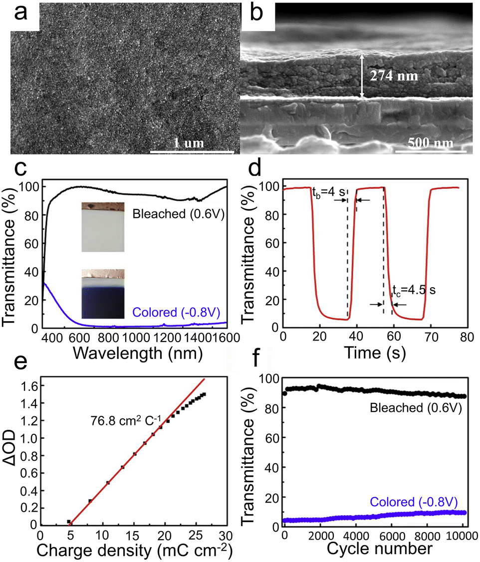 | ||
| Fig. 5 (a) Surface and (b) cross-sectional SEM images of WO3 QDs films. (c) Transmittance spectra in bleached and colored states. (d) Response time at 633 nm. (e) Coloration efficiency at 633 nm. (f) Cycle performance performed between 0.6 V (10 s) and −0.8 V (10 s) at 633 nm. Reproduced from ref. 26 with permission from Elsevier, Copyright 2020. | ||
1D WO3 nanostructures (such as nanowires, nanorods, nanotubes, and so on) with high porosity and length–diameter ratios are beneficial for transporting ions and electrons to enhance the EC properties.28,133–137 Heo et al.133 fabricated mesoporous thin films of different aspect ratios of WO2.72 nanorods by a low-temperature and template-free method, as shown in Fig. 6a and b. The construction of WO2.72 nanorod films with anisotropic morphology is mainly due to the presence of electrostatic repulsion forces after ligand-stripping, which prevent close-packing of the nanorods. This method without annealing is a useful strategy to prepare EC films on flexible substrates. Besides, a framework could be provided by the anisotropic and mesoporous morphology of WO2.72 nanorods films to introduce guest components to fabricate nanocomposite films. For example, the authors prepared WOx/NbOx composite film by the spin-coating method on WO2.72 high aspect ratio nanorod film. The composite film has the capability of optical modulation in the visible–NIR band and fast switching kinetics. The superior EC performance can be attributed to the high porosity of high aspect ratio and anisotropic nanorods, which enlarge the WOx/NbOx interface and lower the barrier on it. Therefore, the kinetics of Li+ extraction and charge transfer have been improved. This method enables adjustment of the porosity as well as retaining of nanocrystal properties by controlling the aspect ratios of nanorods via a low-temperature process, which may be an effective strategy for preparing EC films on flexible substrates. Huang et al.19 prepared WO3 films with the shape of nanorod and nanoflake by the hydrothermal method, as shown in Fig. 6c and d. The two WO3 films with different morphologies were both hexagonal crystal structures, and the diameter of nanorods and thickness of the nanoflakes were very similar. Comparing the EC performance of WO3 nanorod and nanoflake films, the optical modulation ranges were 72% and 61% (Fig. 6e), the coloration times were 3 s and 9 s, the bleaching times were 2.2 s and 7 s (Fig. 6f), and the coloration efficiencies were 67.6 and 53.8 cm2 C−1, respectively. The transmission of the bleached state of WO3 nanorod film was higher than nanoflake film, which shows the scattering difference related to the nanostructures. Compared with the nanoflake film, the capacitive effect of the nanorod film accounted for more energy, which can be attributed to the larger surface area. Meanwhile, both diffusion coefficients were similar. In a word, the large surface area and fast electron transfer kinetics of the nanorod film resulted in a high capacitance contribution, quick redox reactions, and excellent EC characteristics. In addition, the ECD based on WO3 nanorods exhibited excellent EC performance and charging capacity, which provides a new choice for Zn2+-based ECDs.
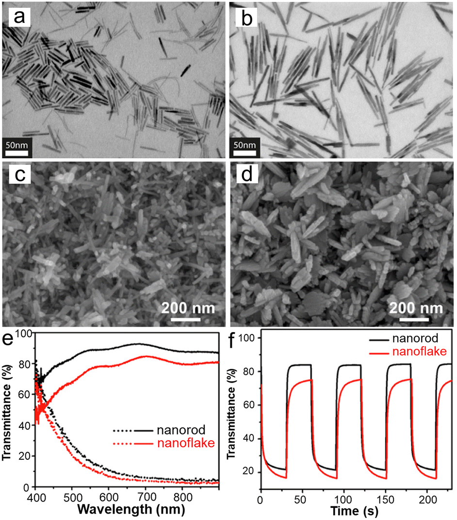 | ||
| Fig. 6 Scanning transmission electron microscope (STEM) images of WO2.72 nanorods. (a) Low aspect ratios of nanorods. (b) High aspect ratios of nanorods. Reproduced from ref. 133 with permission from American Chemical Society, Copyright 2017. SEM images of (c) WO3 nanorods and (d) WO3 nanoflakes film. (e) Transmittance spectra at colored (dot line) and bleached (solid line) states. (f) Real-time transmittance changes were measured at 550 nm. Reproduced from ref. 19 with permission from Elsevier, Copyright 2021. | ||
2D nanostructures mainly refer to nanosheets and nanoflakes, which have the advantages of a large active area, stability, and good film-forming ability, and are appropriate for fabricating EC films at a low cost.29,138–140 Azam et al.29 fabricated WO3 nanosheets with a high aspect ratio by exfoliating bulk WS2 and subsequently taking chemical oxidation for EC application, as shown in Fig. 7a–f. The WO3 nanosheets were separated into two regimes of thickness, below 20 nm and 20–50 nm. Besides, the WO3 film was also prepared using commercial WO3 powder with an average particle size of 131 nm. Comparing the optical transmittance modulation range (Fig. 7b and c) and response time (Fig. 7e and f) of the WO3 nanosheets with the commercial WO3 powder, the WO3 nanosheets exhibited better electrochromic performance. When the nanosheets are used to prepare EC films, permeable channels will be opened between the nanosheets, significantly increasing the surface area exposed to the electrolyte. The larger interface supplies more active sites for Li+. Thus, the Li-ion diffusion length and the barrier of intercalate/extraction (ion/charge dual-insertion/extraction) are greatly reduced during the EC process. The thin nanosheets layer has the best EC properties because, in comparison with the bulk WO3 powder and thick WO3 nanosheets, it has a bigger electrochemical surface area, more Li+ access sites, and a fast ion diffusion coefficient. Additionally, WO3 thin nanosheets with a high aspect ratio can form a homogeneous and sticky coating that supports the long-term stability of ECDs.
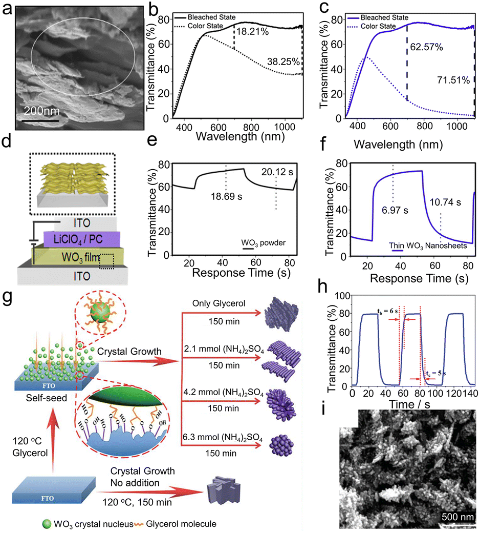 | ||
| Fig. 7 (a) SEM image of cross-sectional WO3 film. Optical transmittance spectra of (b) WO3 powder and (c) thin WO3 nanosheets. (d) Schematic of WO3 EC device; inset shows layer by layer film formation of WO3 nanosheets. Switching response time of (e) WO3 powder and (f) thin WO3 nanosheets. Reproduced from ref. 29 with permission from the American Chemical Society, Copyright 2018. (g) Schematic illustration of the process of glycerol self-seeded growth. (h) Transmittance curves and switching time between colored and bleached states at 630 nm. (i) SEM images of porous coral-like WO3 film. Reproduced from ref. 30 with permission from the Royal Society of Chemistry, Copyright 2019. | ||
3D nanostructures usually require complicated synthetic processes. However, because of their unique structure and extension in different directions, they are able to demonstrate the desired EC performance at short distances of ion diffusion and charge transfer, as well as a vast area of exposure.30,31,141–143 Pan et al.30 prepared WO3 films by a hydrothermal synthesis combining the self-seeded agent glycerol with the capping agent (NH4)2SO4, as shown in Fig. 7g. The coral-like hexagonal WO3 (h-WO3) film (Fig. 7i) was fabricated through the synergistic effect of the glycerol and (NH4)2SO4, which showed a large optical modulation (78.1%), fast switching time (tc = 5 s and tb = 6 s, shown in Fig. 7h), high coloration efficiency (56.5 cm2 C−1) and excellent long-term stability (15000 cycles without obvious decay). The large specific surface area and dendritic structure of the porous coral-like nanostructure provides more redox reaction sites. In terms of the ion intercalate/de-intercalate process, the ideal hexagonal crystal and unique coral-like nanostructure lead to high Li+ mobility. The glycerol improves the direct adhesion between the WO3 film and FTO as well as the potential interlocking force between dendrites, which contributes to the film's excellent cycling stability. Meanwhile, the abundant ordered ion channels and fluffy porous morphology are also beneficial for stability, helping to transfer ions and efficiently remove impact stress during the EC process. In summary, the significant EC performance is due to a large specific surface area, more redox reaction sites, and ion channels supplied by the specific coral-like h-WO3 nanostructure. Particular 3D nanostructures can increase the contact area between the electrode and electrolyte, improve ion transport inside the structure, and facilitate the insertion/extraction of ions.
Zhao et al.32 fabricated WO3 film with controlled crystallinity (WO3-CC) by simple single-step RF magnetron sputtering. The WO3-CC film with high crystallinity near the substrates to a highly disordered structure near the surface across the film thickness was prepared by adjusting the temperature of the substrate during the preparation process, as shown in Fig. 8a. The EC properties of the WO3-CC film include a large optical modulation (72.5% at 1000 nm) and fast switching speed (5.3 s for coloration and 3.0 s for bleaching) in near-infrared regions, as shown in Fig. 8c and d. More importantly, the optical modulation range and switching response time of WO3-CC are close to the amorphous WO3, while the cycling stability is near to that of the crystalline WO3 prepared by the same method. Huo et al.34 synthesized aligned hexagonal/amorphous WO3 core/shell nanorod arrays (h@a-WNRAs) by hydrothermal treatment and spin coating. The prepared samples were divided into WT 250-0.075, WT 250-0.15, and WT 250-0.3 according to the concentrations of WOx precursor solutions, and the WT refers to the sample without an amorphous shell. As shown in Fig. 8e–g, an amorphous WO3 shell of suitable thickness is beneficial for the EC performance of hexagonal WO3, including a larger optical modulation range and shorter switching time. The improvements in EC properties of h@a-WNRAs are mainly attributed to the combination of the high specific surface area and porous structure of amorphous WOx with the stability of hexagonal WO3. Undoubtedly, adjusting the crystallinity of WO3 through specific strategies to take advantage of both crystalline/amorphous states of WO3 has important significance for obtaining the ideal WO3 EC films.
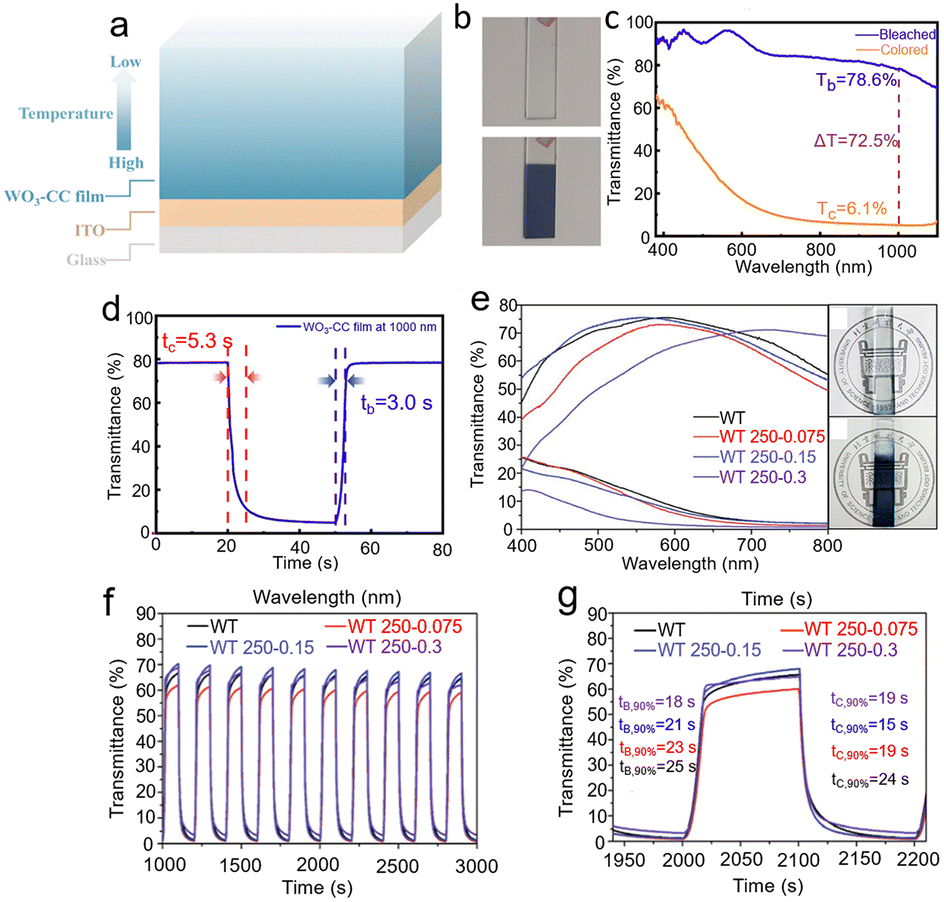 | ||
| Fig. 8 (a) Schematic of the WO3 film with controllable crystallinity. (b) The photos of the WO3-CC film in the bleached state and the colored state. (c) Optical transmittance spectra and (d) switching response curves of WO3-CC film. Reproduced from ref. 32 with permission from the American Chemical Society, Copyright 2020. (e) The visible transmittance spectra of samples and pictures of WT 250-0.15. (f) The in situ response curves of samples between +3.0 V and −3.0 V for 100 s per step at 660 nm. (g) The response times of samples. Reproduced from ref. 34 with permission from the Royal Society of Chemistry, Copyright 2019. | ||
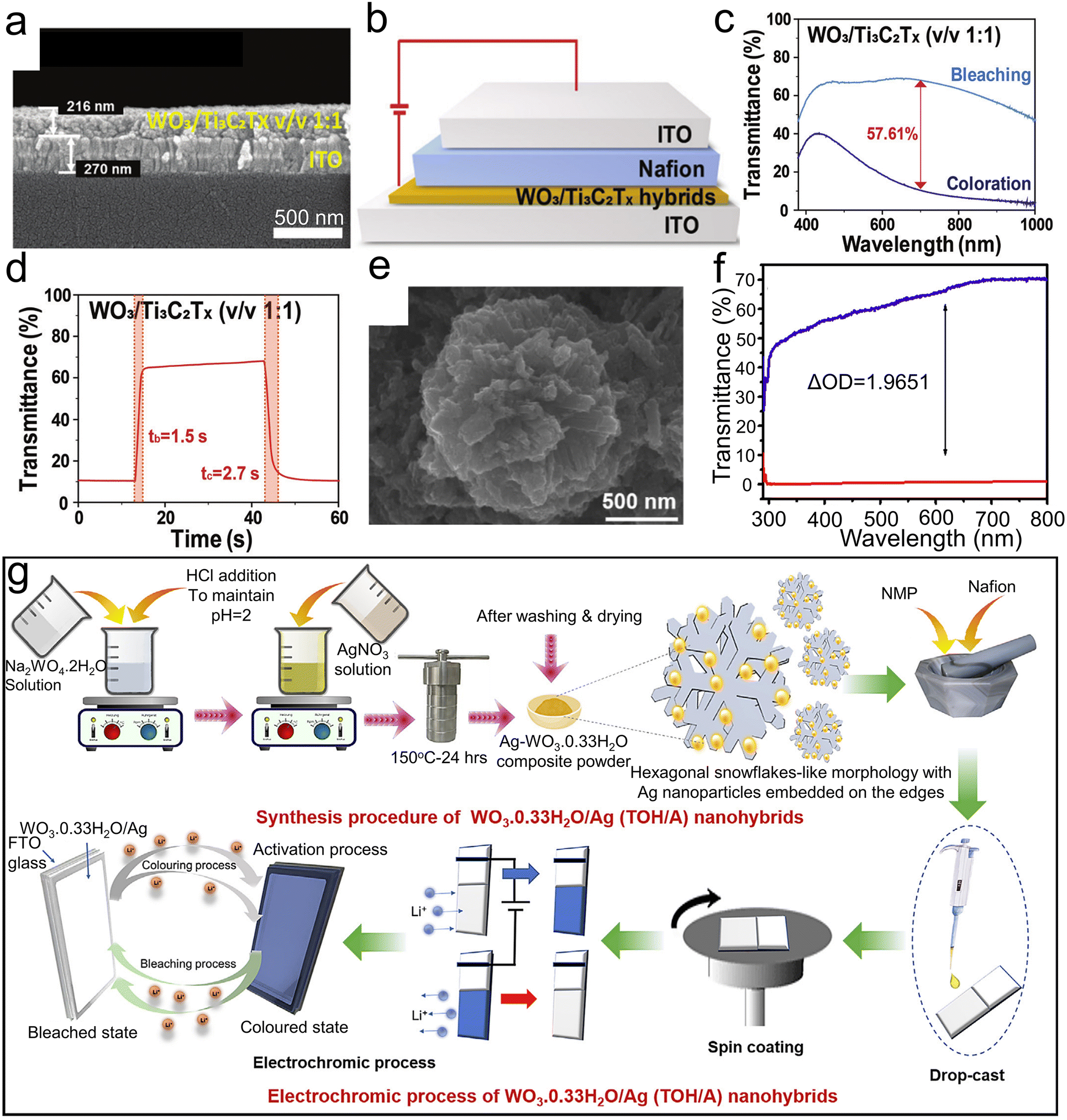 | ||
| Fig. 9 (a) SEM images of a cross-sectional view of WO3/Ti3C2Tx hybrid v/v 1:1 film coated on ITO glasses. (b) EC device based on WO3/Ti3C2Tx hybrid film. (c) Transmittance spectra of EC device based on WO3/Ti3C2Tx. (d) In situ switching curve at 700 nm of WO3/Ti3C2Tx (v/v 1:1)-based EC devices. Reproduced from ref. 49 with permission from the Royal Society of Chemistry, Copyright 2021. (e) FESEM images of TOH/A-2. (f) Optical transmittance spectra of colored and bleached states of TOH/A-2. (g) Schematic of synthesis procedure, thin film preparation, and electrochromic process of TOH/A nanohybrids. Reproduced from ref. 126 with permission from Elsevier, Copyright 2021. | ||
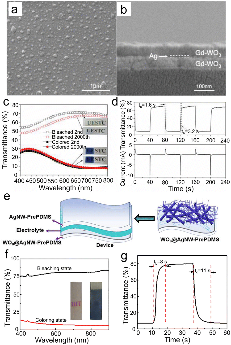 | ||
| Fig. 10 SEM images of (a) surface and (b) cross-sectional microstructures of the WGd-Ag-WGd film. (c) Optical transmittance spectra of the colored and bleached states of the WGd-Ag-WGd sample. The inset shows the corresponding images of bleached (top) and colored (bottom) states after the 2000th cycling. (d) Corresponding in situ transmittance curve at 633 nm to CA curve. Reproduced from ref. 21 with permission from the Royal Society of Chemistry, Copyright 2020. (e) The wearable WO3@AgNW-PrePDMS devices. (f) Transmittance spectra and (g) switching time at 550 nm of WO3@AgNW-PrePDMS. Reproduced from ref. 37 with permission from Elsevier, Copyright 2021. | ||
4. Conclusions and prospects
We have briefly described the general structure of the electrochromic device and the impact of various electrolyte ions (such as Li+ and Al3+), and then presented the key metrics (optical modulation, switching time, coloration effectiveness, long-term and cycling stability, and memory effect) for assessing the electrochromic device's performance. Several methods for preparing WO3-based EC films were described according to their advantages and disadvantages. In addition, four typical methods for enhancing the electrochromic qualities of WO3-based films or devices have been thoroughly discussed.Researchers have put forward additional techniques and approaches as their studies in making WO3 films and enhancing their EC features have continued to deepen. Several novel design and manufacturing approaches for electrochromic devices have been investigated to adapt to different application scenarios. However, despite extensive study and significant advancements, there are still issues that are unclear and that must be solved in the electrochromic field. Although low crystallinity and a large reactive area can bring fast switching response speed, poor adhesion between the film and substrate, non-ideal stability, and some undesirable side reactions cannot be ignored in the real EC process. Therefore, to obtain EC films with large optical modulation, fast switching response time, and good long-term stability, new strategies for designing and constructing specific compositions and composite structures of WO3-based EC materials based on nanotechnology should be explored urgently.
The creation of high-performance WO3 EC films in large quantities at a reasonable cost is now crucial for the development of electrochromic devices and their industrial application. Sol–gel, electrospinning, electrodeposition, CVD, hydrothermal, and other conventional methods of WO3 nanomaterial preparation and film formation can be used to fabricate specific nanostructures or nanocomposite structures, but they have several drawbacks that make them unsuitable for producing EC films for next-generation ECDs. As a result, both ways to enhance conventional preparation techniques and new techniques (such as ink-jet printing technology and the roll-to-roll process) need to be thoroughly investigated. Unfortunately, there is still a long way to go before finding the right solutions that can readily manage morphology, structure, and thickness while producing large-area EC films based on WO3 at a cheap cost. WO3 EC film's performance attenuation mechanisms, such as internal stress and strain, structural variations, shallow and deep ion traps, etc., also require more experimental investigation under various operating situations in order to produce the optimum electrochromic layer.
Currently, the majority of WO3-based ECDs described have issues that make them unsuitable for practical applications, including poor regulation in the visible and NIR dual-waveband, a lack of long-term resistance in natural environments, monotonous color, and low integration. In addition, the high cost and color halos of large area electrochromic devices also hinder their commercial application. Due to the interaction between various levels in the multilayer structure of ECDs, appropriate device structure is also essential for extending the use scenario and improving the practicability of ECDs. The performance and stabilities of an ECD may be considerably improved by properly synthesizing the substrate, transparent conductive layer, electrolyte layer, and ion storage layer, as well as by designing the complete structure well.
Researchers have recently become quite interested in flexible ECDs because of their potential to be wearable and embeddable. Flexible and portable ECDs are fascinating, but because of their complicated preparation processes and the need to endure extended bending and stretching, they also present more challenges. For WO3 flexible ECDs, several strategies to improve EC performance have developed, such as fabricating specific nanostructures,162 using a metal conductive layer (Ag) instead of FTO/ITO film,14 combining with other EC materials,7etc. Because organic flexible substrates are not heat-resistant, it is crucial to prepare WO3 EC films at moderate temperatures. Additionally, it might be difficult to keep the ECDs’ various layers coherent when they are being bent and stretched repeatedly. However, as smart wearable technology advances, flexible ECDs will become increasingly common due to their flexible design and functionalities.
WO3-based multi-color tunable ECDs can exhibit a strong color tunability with wide color gamut distribution or generate asymmetric coloration changes.163,164 Insertion of a metal layer and construction of a particular interface between the WO3 layer and the metal layer are the keys to multi-color tunable ECDs. The color monotony of conventional WO3 electrochromic devices is remedied by this type of device, which substantially expands the color display spectrum of TMO electrochromic materials. Inorganic electrochromism research will take a new turn thanks to the WO3-based multi-color tunable ECDs, while a wider range of potential application situations are anticipated. WO3-based dual-functional ECDs, which mainly refer to electrochromic energy storage devices, can display a varied degree of color fluctuation depending on the stored energy. With the use of the energy-storing ECDs based on the pseudocapacitance of WO3 film, energy states may be accurately seen. Compared with conventional supercapacitors, WO3 EC supercapacitors are not superior in capacity because the low energy density is required for fast switching time and high coloration efficiency. However, flexible EC supercapacitors have excellent potential for wearable supercapacitors. To control the brightness and temperature of solar radiation, there are dual-band tunable ECDs of visible–NIR light that can dynamically adjust the transmittance of visible and near-infrared light based on the applied voltage. Currently, multi-layer composite EC films or symmetric devices are used to produce WO3-based dual-band ECDs. The production of effective and affordable dual-band ECDs is crucial for the commercialization and acceptability of EC windows.
In conclusion, the EC layer is the most important part of ECDs and the foundation of electrochromism. Many researchers are looking for excellent preparation and enhancement approaches for WO3-based EC films despite several obstacles. Consequently, it is highly anticipated that a growing number of excellent WO3-based EC films will be developed and utilized for next-generation multifunctional ECDs.
Conflicts of interest
There are no conflicts to declare.Acknowledgements
This work was supported by the National Natural Science Foundation of China (grant no. 51902292 and 51702291), the China Postdoctoral Science Foundation (grant no. 2019M662525, 2020TQ0278 and 2020M672282) and the Postdoctoral Research Grant in Henan Province (grant no. 19030019).References
- C. G. Granqvist, M. A. Arvizu, B. Pehlivan, H. Y. Qu, R. T. Wen and G. A. Niklasson, Electrochim. Acta, 2018, 259, 1170–1182 CrossRef CAS.
- N. Hirst, Buildings and climate change, 2013, vol. 9781447147 Search PubMed.
- K. Wang, Q. Meng, Q. Wang, W. Zhang, J. Guo, S. Cao, A. Y. Elezzabi, W. W. Yu, L. Liu and H. Li, Adv. Energy Sustainability Res., 2021, 2, 2100117 CrossRef.
- T. J. Richardson, J. L. Slack and M. D. Rubin, Electrochim. Acta, 2001, 46, 2281–2284 CrossRef CAS.
- S. K. Deb, Appl. Opt., 1969, 8, 192 CrossRef PubMed.
- M. Pan, Y. Ke, L. Ma, S. Zhao, N. Wu and D. Xiao, Electrochim. Acta, 2018, 266, 395–403 CrossRef CAS.
- Z. Shao, A. Huang, C. Ming, J. Bell, P. Yu, Y.-Y. Sun, L. Jin, L. Ma, H. Luo, P. Jin and X. Cao, Nat. Electron., 2022, 5, 45–52 CrossRef CAS.
- L. M. Huang, C. Y. Peng, C. W. Hu, H. C. Lu, C. H. Chen, D. J. Yang, C. C. Kuo and K. C. Ho, Sol. Energy Mater. Sol. Cells, 2017, 171, 258–266 CrossRef CAS.
- V. Rai, R. S. Singh, D. J. Blackwood and D. Zhili, Adv. Eng. Mater., 2020, 22, 2000082 CrossRef CAS.
- D. Zhou, D. Xie, X. Xia, X. Wang, C. Gu and J. Tu, Sci. China Chem., 2017, 60, 3–12 CrossRef CAS.
- A. Bhatt and A. R. Tanna, in International Research Conference on Innovations, Startup and Investments (ICOSTART-2019), 2019, pp. 73–78.
- W. Wu, M. Wang, J. Ma, Y. Cao and Y. Deng, Adv. Electron. Mater., 2018, 4, 1800185 CrossRef.
- W. Wu, H. Fang, H. Ma, L. Wu, Q. Wang and H. Wang, ACS Appl. Mater. Interfaces, 2021, 13, 20326–20335 CrossRef CAS.
- Y. Wang, Z. Meng, H. Chen, T. Li, D. Zheng, Q. Xu, H. Wang, X. Y. Liu and W. Guo, J. Mater. Chem. C, 2019, 7, 1966–1973 RSC.
- G. Zhang, K. Guo, X. Shen, H. Ning, H. Liang, J. Zhong, W. Xu, B. Tang, R. Yao and J. Peng, ACS Appl. Mater. Interfaces, 2021, 13, 4768–4776 CrossRef CAS PubMed.
- G. Luo, L. Shen, J. Zheng and C. Xu, J. Mater. Chem. C, 2017, 5, 3488–3494 RSC.
- A. Hasani, Q. Van Le, T. P. Nguyen, K. S. Choi, W. Sohn, H. W. Jang and S. Y. Kim, Electrochim. Acta, 2018, 283, 1195–1202 CrossRef CAS.
- C. Y. Jeong, H. Watanabe and K. Tajima, Electrochim. Acta, 2021, 389, 138764 CrossRef CAS.
- Q. Huang, S. Cao, Y. Liu, Y. Liang, J. Guo, R. Zeng, J. Zhao and B. Zou, Sol. Energy Mater. Sol. Cells, 2021, 220, 110853 CrossRef CAS.
- X. Huo, X. Miao, X. Han, S. Tang, M. Zhang and M. Guo, J. Mater. Chem. A, 2020, 8, 9927–9938 RSC.
- Y. Yin, T. Gao, Q. Xu, G. Cao, Q. Chen, H. Zhu, C. Lan and C. Li, J. Mater. Chem. A, 2020, 8, 10973–10982 RSC.
- S. Poongodi, P. S. Kumar, D. Mangalaraj, N. Ponpandian, P. Meena, Y. Masuda and C. Lee, J. Alloys Compd., 2017, 719, 71–81 CrossRef CAS.
- L. Zhao, X. Huang, G. Lin, Y. Peng, J. Chao, L. Yi, X. Huang, C. Li and W. Liao, Chem. Eng. J., 2021, 420, 129871 CrossRef CAS.
- J. Kim, A. I. Inamdar, Y. Jo, S. Cho, A. T. A. Ahmed, B. Hou, S. Cha, T. G. Kim, H. Kim and H. Im, J. Mater. Chem. A, 2020, 8, 13459–13469 RSC.
- K. Tang, Y. Zhang, Y. Shi, J. Cui, X. Shu, Y. Wang, Y. Qin, J. Liu, H. H. Tan and Y. Wu, Appl. Surf. Sci., 2019, 498, 143796 CrossRef CAS.
- Y. Yao, Q. Zhao, W. Wei, Z. Chen, Y. Zhu, P. Zhang, Z. Zhang and Y. Gao, Nano Energy, 2020, 68, 104350 CrossRef CAS.
- B. R. Koo, M. H. Jo, K. H. Kim and H. J. Ahn, Chem. Eng. J., 2021, 424, 130383 CrossRef CAS.
- A. V. Kadam, Mater. Today: Proc., 2020, 23, 352–358 CAS.
- A. Azam, J. Kim, J. Park, T. G. Novak, A. P. Tiwari, S. H. Song, B. Kim and S. Jeon, Nano Lett., 2018, 18, 5646–5651 CrossRef CAS PubMed.
- J. Pan, Y. Wang, R. Zheng, M. Wang, Z. Wan, C. Jia, X. Weng, J. Xie and L. Deng, J. Mater. Chem. A, 2019, 7, 13956–13967 RSC.
- Y. Li, W. A. McMaster, H. Wei, D. Chen and R. A. Caruso, ACS Appl. Nano Mater., 2018, 1, 2552–2558 CrossRef CAS.
- Y. Zhao, X. Zhang, X. Chen, W. Li, L. Wang, F. Ren, J. Zhao, F. Endres and Y. Li, ACS Sustainable Chem. Eng., 2020, 8, 11658–11666 CrossRef CAS.
- Y. Shi, M. Sun, Y. Zhang, J. Cui, Y. Wang, X. Shu, Y. Qin, H. H. Tan, J. Liu and Y. Wu, Sol. Energy Mater. Sol. Cells, 2020, 212, 110579 CrossRef CAS.
- X. Huo, H. Zhang, W. Shen, X. Miao, M. Zhang and M. Guo, J. Mater. Chem. A, 2019, 7, 16867–16875 RSC.
- K. Bon-Ryul, K. H. Kim and H. J. Ahn, Nanoscale, 2019, 11, 3318–3325 RSC.
- L. Shen, J. Zheng and C. Xu, Nanoscale, 2019, 11, 23049–23057 RSC.
- T. Hao, S. Wang, H. Xu, X. Zhang, J. Xue, S. Liu, Y. Song, Y. Li and J. Zhao, Chem. Eng. J., 2021, 426, 130840 CrossRef CAS.
- Y. Shi, Y. Zhang, K. Tang, J. Cui, X. Shu, Y. Wang, J. Liu, Y. Jiang, H. H. Tan and Y. Wu, Chem. Eng. J., 2019, 355, 942–951 CrossRef CAS.
- K. A. Gesheva, T. M. Ivanova and G. K. Bodurov, J. Phys.: Conf. Ser., 2014, 559, 012002 CrossRef.
- G. Cai, P. Darmawan, M. Cui, J. Chen, X. Wang, A. L. S. Eh, S. Magdassi and P. S. Lee, Nanoscale, 2016, 8, 348–357 RSC.
- D. Qiu, H. Ji, X. Zhang, H. Zhang, H. Cao, G. Chen, T. Tian, Z. Chen, X. Guo, L. Liang, J. Gao and F. Zhuge, Inorg. Chem., 2019, 58, 2089–2098 CrossRef CAS PubMed.
- H. Gu, C. Guo, S. Zhang, L. Bi, T. Li, T. Sun and S. Liu, ACS Nano, 2018, 12, 559–567 CrossRef CAS PubMed.
- L. Xie, S. Zhao, Y. Zhu, Q. Zhang, T. Chang, A. Huang, P. Jin, S. Ren and S. Bao, ACS Sustainable Chem. Eng., 2019, 7, 17390–17396 CrossRef CAS.
- T. Y. Yun, X. Li, J. Bae, S. H. Kim and H. C. Moon, Mater. Des., 2019, 162, 45–51 CrossRef CAS.
- X. Zhang, J. Zeng, Z. Xu, M. Zhu and P. Liu, New J. Chem., 2021, 45, 5503–5508 RSC.
- Z. Xue, Q. Li, M. Yu, Y. Lv, H. Sun, Y. Zhang and D. Wang, Phys. Lett. A, 2020, 384, 126822 CrossRef CAS.
- A. Zimmer, M. Tresse, N. Stein, D. Horwat and C. Boulanger, Electrochim. Acta, 2020, 360, 136931 CrossRef CAS.
- K. Tajima, H. Watanabe, M. Nishino and T. Kawamoto, J. Ceram. Soc. Jpn., 2020, 128, 381–386 CrossRef CAS.
- V. T. Nguyen, B. K. Min, S. K. Kim, Y. Yi and C. G. Choi, J. Mater. Chem. C, 2021, 9, 3183–3192 RSC.
- P. Cossari, M. Pugliese, C. Simari, A. Mezzi, V. Maiorano, I. Nicotera and G. Gigli, Adv. Mater. Interfaces, 2020, 7, 1901663 CrossRef CAS.
- J. Ding, Z. Liu, A. Wei, T. P. Chen and H. Zhang, Mater. Sci. Semicond. Process., 2018, 88, 73–78 CrossRef CAS.
- J. Guo, M. Wang, X. Diao, Z. Zhang, G. Dong, H. Yu, F. Liu, H. Wang and J. Liu, J. Phys. Chem. C, 2018, 122, 19037–19043 CrossRef CAS.
- X. Chen, W. Li, L. Wang, Y. Zhao, X. Zhang, Y. Li and J. Zhao, Mater. Chem. Phys., 2021, 270, 124745 CrossRef CAS.
- S. Wang, H. Xu, J. Zhao and Y. Li, Inorg. Chem. Front., 2022, 9, 514–523 RSC.
- Z. Wang, K. Shen, H. Xie, B. Xue, J. Zheng and C. Xu, Chem. Eng. J., 2021, 426, 131314 CrossRef CAS.
- M. Wang, Y. He, M. Da Rocha, A. Rougier and X. Diao, Sol. Energy Mater. Sol. Cells, 2021, 230, 111239 CrossRef CAS.
- G. Yang, Y. M. Zhang, Y. Cai, B. Yang, C. Gu and S. X. A. Zhang, Chem. Soc. Rev., 2020, 49, 8687–8720 RSC.
- P. Yang, P. Sun and W. Mai, Mater. Today, 2016, 19, 394–402 CrossRef CAS.
- M. A. Arvizu, H. Y. Qu, U. Cindemir, Z. Qiu, E. A. Rojas-González, D. Primetzhofer, C. G. Granqvist, L. Österlund and G. A. Niklasson, J. Mater. Chem. A, 2019, 7, 2908–2918 RSC.
- D. Xi, J. Wang and X. Guo, Biosci. Rep., 2009, 167, 106502 Search PubMed.
- H. Y. Qu, E. A. Rojas-González, C. G. Granqvist and G. A. Niklasson, Thin Solid Films, 2019, 682, 163–168 CrossRef CAS.
- V. H. V. Quy, I. R. Jo, S. H. Kang and K. S. Ahn, J. Ind. Eng. Chem., 2021, 94, 264–271 CrossRef CAS.
- C. Hua, Z. Cheng, Y. Ma, H. He, G. Xu, Y. Liu, S. Yang and G. Han, J. Electrochem. Soc., 2021, 168, 042503 CrossRef CAS.
- A. Hu, Z. Jiang, C. Kuai, S. McGuigan, D. Nordlund, Y. Liu and F. Lin, J. Mater. Chem. A, 2020, 8, 20000–20010 RSC.
- K. W. Kim, T. Y. Yun, S. H. You, X. Tang, J. Lee, Y. Seo, Y. T. Kim, S. H. Kim, H. C. Moon and J. K. Kim, NPG Asia Mater., 2020, 12, 84 CrossRef CAS.
- L. Pan, Q. Han, Z. Dong, M. Wan, H. Zhu, Y. Li and Y. Mai, Electrochim. Acta, 2019, 328, 135107 CrossRef CAS.
- C. J. Tang, J. L. He, C. C. Jaing, C. J. Liang, C. H. Chou, C. Y. Han and C. L. Tien, Coatings, 2019, 9, 9 CrossRef.
- S. J. Lee, D. S. Choi, S. H. Kang, W. S. Yang, S. Nahm, S. H. Han and T. Kim, ACS Sustainable Chem. Eng., 2019, 7, 7111–7117 CrossRef CAS.
- K. L. Zhou, H. Wang, J. Liu and H. Yan, Int. J. Electrochem. Sci., 2018, 13, 7335–7346 CrossRef CAS.
- K. Pandurangarao, N. Purnachand and V. Ravi Kumar, Opt. Mater., 2020, 101, 109791 CrossRef CAS.
- H. Yu, J. Guo, C. Wang, J. Zhang, J. Liu, G. Dong, X. Zhong and X. Diao, Electrochim. Acta, 2020, 332, 135504 CrossRef CAS.
- A. Semenova, A. Eruzin, P. Bezrukov, M. Sychov, S. Mjakin, T. Lukashova and N. Sudar, Mater. Today: Proc., 2019, 30, 606–610 Search PubMed.
- K. Tajima, H. Watanabe, M. Nishino and T. Kawamoto, RSC Adv., 2020, 10, 2562–2565 RSC.
- B. W. C. Au and K. Y. Chan, Surf. Eng., 2020, 36, 94–99 CrossRef CAS.
- J. Y. Zheng, A. U. Pawar, C. W. Kim, Y. J. Kim and Y. S. Kang, Appl. Catal., B, 2018, 233, 88–98 CrossRef CAS.
- C. M. Chang, Y. C. Chiang, M. H. Cheng, S. H. Lin, W. B. Jian, J. T. Chen, Y. J. Cheng, Y. R. Ma and K. Tsukagoshi, Sol. Energy Mater. Sol. Cells, 2021, 223, 110960 CrossRef CAS.
- H. Kim, K. Kim, D. Choi, M. Lee, W. S. Chu, S. H. Ahn, D. M. Chun and C. S. Lee, Int. J. Precis. Eng. Manuf. – Green Technol., 2018, 5, 231–238 CrossRef.
- K. Mallikarjuna, M. Shinde, A. Kumar, J. Ryu and H. Kim, ACS Sustainable Chem. Eng., 2021, 9, 14559–14568 CrossRef.
- S. Park, D. T. Thuy, S. Sarwar, H. Van Tran, S. I. Lee, H. S. Park, S. H. Song, C. H. Han and S. Hong, J. Mater. Chem. C, 2020, 8, 17245–17253 RSC.
- K. W. Kim, Y. M. Kim, X. Li, T. Ha, S. H. Kim, H. C. Moon and S. W. Lee, Nanomaterials, 2020, 10, 821 CrossRef CAS PubMed.
- C. Wu, Z. Shao, W. Zhai, X. Zhang, C. Zhang, C. Zhu, Y. Yu and W. Liu, ACS Nano, 2022, 16, 2621–2628 CrossRef CAS PubMed.
- W. Cheng, J. He, K. E. Dettelbach, N. J. J. Johnson, R. S. Sherbo and C. P. Berlinguette, Chem, 2018, 4, 821–832 CAS.
- H. Cho, J. Min, D. Won, J. Kwon and S. H. Ko, Acta Mater., 2020, 201, 528–534 CrossRef CAS.
- L. Shen, G. Luo, J. Zheng and C. Xu, Electrochim. Acta, 2018, 278, 263–270 CrossRef CAS.
- A. Khan, N. Y. Bhosale, S. S. Mali, C. K. Hong and A. V. Kadam, J. Colloid Interface Sci., 2020, 571, 185–193 CrossRef CAS PubMed.
- J. Y. Zheng, G. Song, J. Hong, T. K. Van, A. U. Pawar, D. Y. Kim, C. W. Kim, Z. Haider and Y. S. Kang, Cryst. Growth Des., 2014, 14, 6057–6066 CrossRef CAS.
- J. Y. Zheng, G. Song, C. W. Kim and Y. S. Kang, Nanoscale, 2013, 5, 5279–5282 RSC.
- R. Goei, A. J. Ong, T. J. Hao, L. J. Yi, L. S. Kuang, D. Mandler, S. Magdassi and A. I. Y. Tok, Ceram. Int., 2021, 47, 18433–18442 CrossRef CAS.
- M. Arslan, Y. E. Firat, S. R. Tokgöz and A. Peksoz, Ceram. Int., 2021, 47, 32570–32578 CrossRef CAS.
- C. Dulgerbaki and A. U. Oksuz, Opt. Mater., 2021, 119, 111354 CrossRef CAS.
- S. Xie, Z. Bi, Y. Chen, X. He, X. Guo, X. Gao and X. Li, Appl. Surf. Sci., 2018, 459, 774–781 CrossRef CAS.
- M. Rozman, B. Žener, L. Matoh, R. F. Godec, A. Mourtzikou, E. Stathatos, U. Bren and M. Lukšič, Electrochim. Acta, 2020, 330, 135329 CrossRef CAS.
- Y. Zhan, Z. Yang, Z. Xu, Z. Hu, X. Bai, Y. Ren, M. Li, A. Ullah, I. Khan, J. Qiu, Z. Song, B. Liu and Y. Wang, Chem. Eng. J., 2020, 394, 124967 CrossRef CAS.
- Y. Yang, Y. Qi, W. Zhai, J. Tan, S. Feng, J. Zhang, M. Shen, L. Wang, X. Yu and X. Qu, Electron. Mater. Lett., 2020, 16, 424–432 CrossRef CAS.
- Z. Dimitrova and D. Gogova, Mater. Res. Bull., 2005, 40, 333–340 CrossRef CAS.
- J. E. Crowell, J. Vac. Sci. Technol., A, 2003, 21, S88–S95 CrossRef CAS.
- H. Uchiyama, Y. Nakamura and S. Igarashi, RSC Adv., 2021, 11, 7442–7449 RSC.
- K. Wang, H. Zhang, G. Chen, T. Tian, K. Tao, L. Liang, J. Gao and H. Cao, J. Alloys Compd., 2021, 861, 158534 CrossRef CAS.
- W. Li, X. Zhang, X. Chen, Y. Zhao, L. Wang, D. Liu, X. Li, M. Chen, J. Zhao and Y. Li, Mater. Lett., 2020, 265, 127464 CrossRef CAS.
- N. Akkurt, S. Pat, S. Elmas and Ş. Korkmaz, J. Mater. Sci.: Mater. Electron., 2020, 31, 1293–1301 CrossRef CAS.
- E. Eren, C. Alver, G. Y. Karaca, E. Uygun and A. U. Oksuz, Synth. Met., 2018, 235, 115–124 CrossRef CAS.
- X. Li, Z. Li, W. He, H. Chen, X. Tang, Y. Chen and Y. Chen, Coatings, 2021, 11, 959 CrossRef CAS.
- P. J. Kelly and R. D. Arnell, Vacuum, 2000, 56, 159–172 CrossRef CAS.
- H. Najafi-Ashtiani, B. Akhavan, F. Jing and M. M. Bilek, ACS Appl. Mater. Interfaces, 2019, 11, 14871–14881 CrossRef CAS PubMed.
- D. M. Mattox, Met. Finish., 2000, 98, 410–423 CrossRef.
- A. Chemseddine, M. Henry and J. Livage, Rev. Chim. Miner., 1984, 21, 487–495 CAS.
- S. Zeb, G. Sun, Y. Nie, H. Xu, Y. Cui and X. Jiang, Mater. Adv., 2021, 2, 6839–6884 RSC.
- D. Bokov, A. T. Jalil, S. Chupradit, W. Suksatan, M. J. Ansari, I. H. Shewael, G. H. Valiev and E. Kianfar, Adv. Mater. Sci. Eng., 2021, 2021, 5102014 CrossRef.
- B. B. Lakshmi, C. J. Patrissi and C. R. Martin, Chem. Mater., 1997, 9, 2544–2550 CrossRef CAS.
- A. Kamyshny, Open Appl. Phys. J., 2011, 4, 19–36 CrossRef CAS.
- S. Zhang, S. Chen, F. Hu, R. Xu, B. Yan, M. Jiang, Y. Gu, F. Yang and Y. Cao, Sol. Energy Mater. Sol. Cells, 2019, 200, 109951 CrossRef CAS.
- M. M. Nir, D. Zamir, I. Haymov, L. Ben-Asher, O. Cohen, B. Faulkner and F. D. L. Vega, in The Chemistry of Inkjet Inks, 2009, pp. 225–254 Search PubMed.
- S. Wang, M. Liu, L. Kong, Y. Long, X. Jiang and A. Yu, Prog. Mater. Sci., 2016, 81, 1–54 CrossRef CAS.
- A. Behera, P. Mallick and S. S. Mohapatra, in Corrosion Protection at the Nanoscale, 2020, pp. 227–243 Search PubMed.
- K. Byrappa and T. Adschiri, Prog. Cryst. Growth Charact. Mater., 2007, 53, 117–166 CrossRef CAS.
- S. H. Feng and G. H. Li, in Modern Inorganic Synthetic Chemistry, 2nd edn, 2017, pp. 73–104 Search PubMed.
- D. S. Jayakrishnan, in Corrosion Protection and Control Using Nanomaterials, Woodhead Publishing Limited, 2012, pp. 86–125 Search PubMed.
- C. Li, M. Iqbal, J. Lin, X. Luo, B. Jiang, V. Malgras, K. C. W. Wu, J. Kim and Y. Yamauchi, Acc. Chem. Res., 2018, 51, 1764–1773 CrossRef CAS PubMed.
- M. Mastrangeli, S. Abbasi, C. Varel, C. V. Hoof, J.-P. Celis and K. F. Bohringer, J. Micromech. Microeng., 2009, 19, 083001 CrossRef CAS PubMed.
- K. Thorkelsson, P. Bai and T. Xu, Nano Today, 2015, 10, 48–66 CrossRef CAS.
- G. Decher, Science, 1997, 277, 1232–1237 CrossRef CAS.
- Z. Xie, Q. Liu, Q. Zhang, B. Lu, J. Zhai and X. Diao, Sol. Energy Mater. Sol. Cells, 2019, 200, 110017 CrossRef CAS.
- Y. Song, Z. Zhang, L. Yan, L. Zhang, S. Liu, S. Xie, L. Xu and J. Du, Nanomaterials, 2019, 9, 1795 CrossRef CAS PubMed.
- S. R. Bathe and P. S. Patil, Mater. Sci. Eng., B, 2020, 257, 114542 CrossRef CAS.
- L. Zhou, P. Wei, H. Fang, W. Wu, L. Wu and H. Wang, J. Mater. Chem. C, 2020, 8, 13999–14006 RSC.
- V. G. Deonikar, J. M. C. Puguan and H. Kim, Acta Mater., 2021, 207, 116693 CrossRef CAS.
- Q. Guo, X. Zhao, Z. Li, D. Wang and G. Nie, Chem. Eng. J., 2020, 384, 123370 CrossRef CAS.
- H. Ling, L. P. Yeo, Z. Wang, X. Li, D. Mandler, S. Magdassi and A. I. Y. Tok, J. Mater. Chem. C, 2018, 6, 8488–8494 RSC.
- W. Li, X. Zhang, X. Chen, Y. Zhao, L. Wang, M. Chen, Z. Li, J. Zhao and Y. Li, Electrochim. Acta, 2020, 355, 136817 CrossRef CAS.
- M. Bourdin, I. Mjejri, A. Rougier, C. Labrugère, T. Cardinal, Y. Messaddeq and M. Gaudon, J. Alloys Compd., 2020, 823, 153690 CrossRef CAS.
- H. Kim, D. Choi, K. Kim, W. Chu, D. M. Chun and C. S. Lee, Sol. Energy Mater. Sol. Cells, 2018, 177, 44–50 CrossRef CAS.
- W. Q. Wang, X. L. Wang, X. H. Xia, Z. J. Yao, Y. Zhong and J. P. Tu, Nanoscale, 2018, 10, 8162–8169 RSC.
- S. Heo, J. Kim, G. K. Ong and D. J. Milliron, Nano Lett., 2017, 17, 5756–5761 CrossRef CAS PubMed.
- R. C. Evans, R. Austin, R. C. Miller, A. Preston, Z. N. Nilsson, K. Ma and J. B. Sambur, ACS Appl. Nano Mater., 2021, 4, 3750–3759 CrossRef CAS.
- L. Wang, Y. Liu, G. Han and H. Zhao, J. Alloys Compd., 2022, 890, 161833 CrossRef CAS.
- G. T. Phan, D. Van Pham, R. A. Patil, C. H. Tsai, C. C. Lai, W. C. Yeh, Y. Liou and Y. R. Ma, Sol. Energy Mater. Sol. Cells, 2021, 231, 111306 CrossRef CAS.
- D. Louloudakis, K. Mouratis, J. Gil-Rostra, E. Koudoumas, R. Alvarez, A. Palmero and A. R. Gonzalez-Elipe, Electrochim. Acta, 2021, 376, 138049 CrossRef CAS.
- Z. Xie, Q. Zhang, Q. Liu, J. Zhai and X. Diao, Thin Solid Films, 2018, 653, 188–193 CrossRef CAS.
- X. Chang, R. Hu, S. Sun, T. Lu, T. Liu, Y. Lei, L. Dong, Y. Yin and Y. Zhu, Nanotechnology, 2018, 29, 185707 CrossRef PubMed.
- V. S. Kumbhar, J. Lee, Y. Choi, H. Lee, M. Ryuichi, M. Nakayama, W. Lee, H. Oh and K. Lee, Thin Solid Films, 2020, 709, 138214 CrossRef CAS.
- X. Zhang, S. Dou, W. Li, L. Wang, H. Qu, X. Chen, L. Zhang, Y. Zhao, J. Zhao and Y. Li, Electrochim. Acta, 2019, 297, 223–229 CrossRef CAS.
- S. Wang, H. Xu, T. Hao, P. Wang, X. Zhang, H. Zhang, J. Xue, J. Zhao and Y. Li, NPG Asia Mater., 2021, 13, 51 CrossRef CAS.
- Z. Li, B. Wang, X. Zhao, Q. Guo and G. Nie, New J. Chem., 2020, 44, 20584–20591 RSC.
- Y. Zhao, X. Zhang, W. Li, Z. Li, H. Zhang, M. Chen, W. Sun, Y. Xiao, J. Zhao and Y. Li, Sol. Energy Mater. Sol. Cells, 2022, 237, 111564 CrossRef CAS.
- J. Yuan, B. Wang, H. Wang, Y. Chai, Y. Jin, H. Qi and J. Shao, Appl. Surf. Sci., 2018, 447, 471–478 CrossRef CAS.
- X. Zhang, Y. Tian, W. Li, S. Dou, L. Wang, H. Qu, J. Zhao and Y. Li, Sol. Energy Mater. Sol. Cells, 2019, 200, 109916 CrossRef CAS.
- Z. J. Xia, H. L. Wang, Y. F. Su, P. Tang, M. J. Dai, H. J. Lin, Z. G. Zhang and Q. Shi, Coatings, 2020, 10, 577 CrossRef CAS.
- A. Shirpay and M. M. B. Mohagheghi, J. Mater. Sci., 2021, 56, 14644–14658 CrossRef CAS.
- H. Lyu, Polymers, 2020, 12, 49 CrossRef CAS PubMed.
- W. Q. Wang, Z. J. Yao, X. L. Wang, X. H. Xia, C. D. Gu and J. P. Tu, J. Colloid Interface Sci., 2019, 535, 300–307 CrossRef CAS PubMed.
- W. Thongpan, D. Louloudakis, P. Pooseekheaw, T. Kumpika, E. Kantarak, W. sroila, A. Panthawan, W. Thongsuwan and P. Singjai, Mater. Lett., 2019, 257, 126747 CrossRef CAS.
- S. H. Yang and J. H. Yang, Vacuum, 2020, 179, 109460 CrossRef CAS.
- Q. Zhao, Y. Fang, K. Qiao, W. Wei, Y. Yao and Y. Gao, Sol. Energy Mater. Sol. Cells, 2019, 194, 95–102 CrossRef CAS.
- T. Van Nguyen, H. H. Do, T. Q. Trung, Q. Van Le, T. P. Nguyen, S. H. Hong, H. W. Jang, S. H. Ahn and S. Y. Kim, J. Alloys Compd., 2021, 882, 160718 CrossRef.
- K. H. Kim, B. R. Koo and H. J. Ahn, Ceram. Int., 2019, 45, 15990–15995 CrossRef CAS.
- G. Zhang, K. Lu, X. Zhang, W. Yuan, H. Ning, R. Tao, X. Liu, R. Yao and J. Peng, Coatings, 2018, 8, 228 CrossRef.
- Q. Xu, Y. Yin, T. Gao, G. Cao, Q. Chen, C. Lan, F. Li and C. Li, J. Alloys Compd., 2020, 829, 154431 CrossRef CAS.
- R. Goei, A. J. Ong, J. H. Tan, J. Y. Loke, S. K. Lua, D. Mandler, S. Magdassi and A. I. Y. Tok, ACS Omega, 2021, 6, 26251–26261 CrossRef CAS PubMed.
- S.-H. Yang, G.-Y. Tseng and C.-F. Kao, J. Electrochem. Soc., 2019, 166, 170–176 CrossRef.
- K. Tang, Y. Zhang, Y. Shi, J. Cui, X. Shu, Y. Wang, Y. Qin, J. Liu, H. H. Tan and Y. Wu, Electrochim. Acta, 2020, 330, 135189 CrossRef CAS.
- G. Y. Karaca, E. Eren, G. C. Cogal, E. Uygun, L. Oksuz and A. U. Oksuz, Opt. Mater., 2019, 88, 472–478 CrossRef CAS.
- L. Xiao, Y. Lv, W. Dong, N. Zhang and X. Liu, ACS Appl. Mater. Interfaces, 2016, 8, 27107–27114 CrossRef CAS PubMed.
- Z. Wang, X. Wang, S. Cong, J. Chen, H. Sun, Z. Chen, G. Song, F. Geng, Q. Chen and Z. Zhao, Nat. Commun., 2020, 11, 302 CrossRef CAS PubMed.
- J. Chen, Z. Wang, C. Liu, Z. Chen, X. Tang, Q. Wu, S. Zhang, G. Song, S. Cong, Q. Chen and Z. Zhao, Adv. Mater., 2021, 33, 1–10 Search PubMed.
| This journal is © The Royal Society of Chemistry 2023 |