
 Open Access Article
 This Open Access Article is licensed under a
 Creative Commons Attribution 3.0 Unported Licence
Dielectric behaviour of plasma hydrogenated TiO2/cyanoethylated cellulose nanocomposites†
Nadeesh M.
Adassooriya
 a,
Dilek
Ozgit
a,
Sai G.
Shivareddy
a,
Pritesh
Hiralal
a,
Damayanthi
Dahanayake
b,
Rachel A.
Oliver
c and
Gehan A. J.
Amaratunga
*a
a,
Dilek
Ozgit
a,
Sai G.
Shivareddy
a,
Pritesh
Hiralal
a,
Damayanthi
Dahanayake
b,
Rachel A.
Oliver
c and
Gehan A. J.
Amaratunga
*a
aElectrical Engineering Division, Department of Engineering, University of Cambridge, 9 JJ Thomson Avenue, Cambridge CB3 0FA, UK. E-mail: gaja1@cam.ac.uk; Fax: +44 (0)1223748348; Tel: +44 (0)1223 748325
bSri Lanka Institute of Nanotechnology (SLINTEC), Mahenawatta, Pitipana, Homagama, CO 10206, Sri Lanka
cDepartment of Materials Science and Metallurgy, University of Cambridge, 27 Charles Babbage Road, Cambridge, CB3 0FS, UK
First published on 19th December 2022
Abstract
The interface between the polymer and nanoparticle has a vital role in determining the overall dielectric properties of a dielectric polymer nanocomposite. In this study, a novel dielectric nanocomposite containing a high permittivity polymer, cyanoethylated cellulose (CRS) and TiO2 nanoparticles surface modified by hydrogen plasma treatments was successfully prepared with different weight percentages (10%, 20% and 30%) of hydrogenated TiO2. Internal structure of H plasma treated TiO2 nanoparticles (H-TiO2) and the intermolecular interactions and morphology within the polymer nanocomposites were analysed. H-TiO2/CRS thin films on SiO2/Si wafers were used to form metal–insulator–metal (MIM) type capacitors. Capacitances and loss factors in the frequency range of 1 kHz to 1 MHz were measured. At 1 kHz H-TiO2/CRS nanocomposites exhibited ultra-high dielectric constants of 80, 118 and 131 for nanocomposites with 10%, 20% and 30% weight of hydrogenated TiO2 respectively, significantly higher than values of pure CRS (21) and TiO2 (41). Furthermore, all three H-TiO2 /CRS nanocomposites show a loss factor <0.3 at 1 kHz and low leakage current densities (10−6 A cm−2–10−7 A cm−2). Leakage was studied using conductive atomic force microscopy (C-AFM) and it was observed that the leakage is associated with H-TiO2 nanoparticles embedded in the CRS polymer matrix. Although, modified interface slightly reduces energy densities compared to pristine TiO2/CRS system, the capacitance values for H-TiO2/CRS-in the voltage range of −2 V to 2 V are very stable. Whilst H-TiO2/CRS possesses ultra-high dielectric constants (>100), this study reveals that the polymer nanoparticle interface has a potential influence on dielectric behaviour of the composite.
Introduction
Capacitors are used ubiquitously in all electronic circuits and systems for transient energy storage and ballasting. Energy density achievable in a capacitor will determine its physical size in an electronic system.1 Very often the capacitor size is a limiting factor in minimising the overall size and weight of an electronic system. This is a pressing issue especially in portable and mobile electronic systems in applications ranging from wearable sensors to electric vehicles. At present the higher energy rated are bulky electrolytic capacitors. One promising route to replacing electrolytic capacitors is to have thin film dielectric capacitors with higher energy density.2 In turn, the energy densities of dielectric capacitors are limited by the relative permittivity of the dielectric material. As a result, within the past decade there has been significant research effort directed at developing higher permittivity dielectric materials for capacitors.3One route being explored to achieve high effective permittivity is to form a composite of two (or more in principle) dielectrics. However, the challenge is to achieve an increase in the effective permittivity of the dielectric without increasing its effective thickness, which would reduce capacitance, beyond that required for sustaining the electric field without breakdown at the specified operating voltage. One possible way of achieving this is to introduce one of the materials in nanoparticle form within the other i.e. a nanocomposite.4 This has the advantage of maximising surface (interface) area to volume ratio of the material included in nanoparticle form. In recent years, it has been shown that with the introduction of nanosized fillers into polymer matrices significantly higher dielectric constants compared the dielectric constant of the filler could be achieved. This increase in effective dielectric constant has been ascribed to polarisation phenomena at the nanoparticle–polymer interfaces.5
It is in this vein that nanosized fillers have been introduced into dielectric polymer matrix to form dielectric polymer nanocomposites. Enhanced dielectric properties with low leakage currents while preserving the facile processability, flexibility and lightness of the polymer matrix have been reported.6–8 TiO2 is a versatile material used in a range of applications including nanodielectrics where composites of nanoscale TiO2 with different polymers form the dielectric.9–18 In 1988, Bandyopadhyay et al. reported the first dielectric nanocomposite based on TiO2 nanoparticle and polystyrene.9 Afterwards, in 1994 Lewis10 reported a landmark theoretical study on dielectric nanocomposites the significance which was recognised after publication of the experimental work on TiO2-epoxy resin dielectric nanocomposite (k = 8.5 at 1 kHz for 500–750 μm thick films) published by Nelson et al. in 2002.11 In 2004, Cheng et al. reported a cross linked poly-4-vinylphenol-TiO2 dielectric nanocomposite with dielectric constant of 7.5 at 50 kHz. Maliakal et al. achieved over 3 times enhancement of dielectric constant compared to that of bulk polystyrene for a 1.25 μm thick core shell TiO2–polystyrene nanocomposite films at 1 kHz.12 Nanocomposites of polypyrrole/TiO2 (k = 140 at 1 kHz for 0.5 mm thick films),13 PMMA/TiO2 (k = 25 at 1 kHz for 5 mm thick films),14 poly(vinylidenefluoride-ter-trifluoroethylene)-TiO2 (k = 12 at 1 kHz for 25–50 μm thick films)15 and poly (vinylidenefluoride-ter-trifluoroethylene-ter-chlorotrifluoroethylene)-TiO2 (k = 42 at 1 kHz for 25–50 μm thick films),16 PEOX–PVP–TiO2 nanocomposite (k = 18.56 at 1 kHz 0.40 mm thick films)17 have been reported subsequently in the literature. In our previous work we explored the use of TiO2 nanoparticles within a high dielectric polymer called cyanoethylated cellulose (CRS) and reported effective relative permittivities in excess of 200 ((k = 207 at 1 kHz, 25 nm TiO2 particles, 120 nm thin films); 10 times higher than that of the pristine CRS polymer).18 CRS is a cellulose derivative with very high dielectric constant (k = 21 at 1 kHz) compared to other dielectric polymers, but has received comparatively less attention in the literature. Dipoles of CO and CN present in CRS are responsible for dielectric behaviour and due to the polar nature of the polymer matrix, it also shows a strong affinity for inorganic oxides.19 In addition, dielectric behaviour of CRS/BaTiO3 (k = 133 at 1 kHz, 2-micron BaTiO3 particles and film thickness 100–350 μm)20 and MMT/CRS (k = 71 at 1 kHz, 180 nm thin films)21 have been reported in the literature. Here we further explore the TiO2 nanoparticle system by subjecting the surface to a plasma treatment. The aim is to see whether the effective interface charge density can be enhanced by introducing additional surface states through mild plasma etching.
In the hydrogenation process TiO2 nanoparticles are treated in hydrogen containing environment or hydrogen plasma at defined temperatures for certain period of time. During this process the surface of the TiO2 nanoparticles completely change as it forms a highly disordered surface layer containing large number of oxygen vacancies, Ti3+ though self-doping, surface hydroxyl groups and T–H bonds. Hydrogenated TiO2 or black TiO2 is now one of the most attractive materials in the areas of photocatalysis, electrochemical solar cells, supercapacitors and batteries.22–25
Experimental
Materials
TiO2 anatase nanoparticles and acetone were purchased from Sigma Aldrich, USA and CRS polymer were purchased from Shin-Etsu Chemical Co. Ltd Japan. All chemicals were used without further purification.Hydrogenation of TiO2 NPs using hydrogen plasma
TiO2 nanoparticles (100 mg) were dispersed in ethanol (50 ml) with the aid of ultrasonication for 10 min. Then solution was drop cast on a Si wafer. Drop casting was repeated several times to obtain a thick TiO2 layer on the Si wafer. Prepared TiO2 films were exposed to an H plasma for 2–10 min. The H2 plasma treatment was performed at 500 °C and 3.6 mbar pressure. Plasma power was 50 W and H2 flow rate was 50 sccm.Preparation of films of H plasma treated TiO2 nanocomposite
CRS polymer was dissolved in acetone to prepare a polymer solution and different volumes of polymer solution were mixed with H-TiO2 nanoparticles and stirred for 24 hours to obtain H-TiO2/CRS dispersions with different H-TiO2 weight percentages; 10% (3.45 vol%), 20% (6.65 vol%) and 30% (9.65 vol%) respectively. Spin coating of H-TiO2/CRS dispersions at 2500 rpm for 20 s was used to deposit polymer nanocomposite films on clean n-type Si wafer (with a 200 nm SiO2 layer). This was followed by thermal annealing at 150 °C for 3 hours.Fabrication of metal–insulator–metal (MIM) type capacitors
H-TiO2/CRS nanocomposite films on SiO2/Si wafers were used to form metal–insulator–metal (MIM) type capacitors (100 nm Al layers deposited by thermal evaporation were used as metal top and bottom electrodes). Capacitance measurements of the nanocomposites over a range of frequencies from 1 kHz to 1 MHz, capacitance–voltage measurements and current–voltage measurements were performed on a Microtech cascade probe station.Characterisation H-TiO2/CRS nanocomposite
PXRD data of the dielectric films were collected on a Phillips PW3710 diffractometer with nickel-filtered CuKα radiation (1.5406 Å) using a scanning RTMS X'Celerator detector. The morphology and film thickness were analysed by Scanning Electron Microscopy (SEM) using a HITACHI SS5500 microscope. Conductive atomic force microscopy (C-AFM) was carried out on a Veeco Dimension 3100 atomic force microscope (AFM) using a commercially-available extended tunneling atomic force microscopy (extended-TUNA) module. Platinum–iridium coated probes (from Veeco, model: SCM-PIC) were used. X-ray photoelectron spectroscopy (XPS) was carried out using a ESCALAB 250 Xi equipped with a monochromatic Al Kα X-ray source in an ultrahigh vacuum. Ultra-violet photoemission spectroscopy (UPS) was also carried out using a ESCALAB 250 Xi with a UV excitation source of He–I emission at 21.21 eV in an ultrahigh vacuum. Fourier transform infra-red spectroscopy was performed using a Bruker Vertex80 in the range from 600 to 4000 cm−1 using the attenuated total reflectance technique. Transmission electron microscopy characterisation was performed at room temperature on a Philips CM30 instrument operating at 300 kV. TEM images, electron diffraction patterns and EELs spectra were recorded. NMR Spectrum for hydrogenated TiO2 was recorded on a Bruker Advance 400 spectrometer tuned to 500 MHz for 1H NMR. A 4 mm probe was used spinning at 6 kHz. 1000 transients were collected using an 8 s recycle delay and a rf field of 60 kHz. Elemental analysis (hydrogen) of hydrogenated TiO2 was performed using a CE-440 Exeter Analytical, Inc. elemental analyser. Schematic representation of fabrication of MIM capacitor starting from pristine TiO2 and CRS polymer is given in the Fig. 1. | ||
| Fig. 1 Stepwise preparation of MIM capacitors with H plasma treated TiO2–CRS nanocomposite thin films. | ||
Results and discussion
Hydrogen plasma treated TiO2 nanoparticles
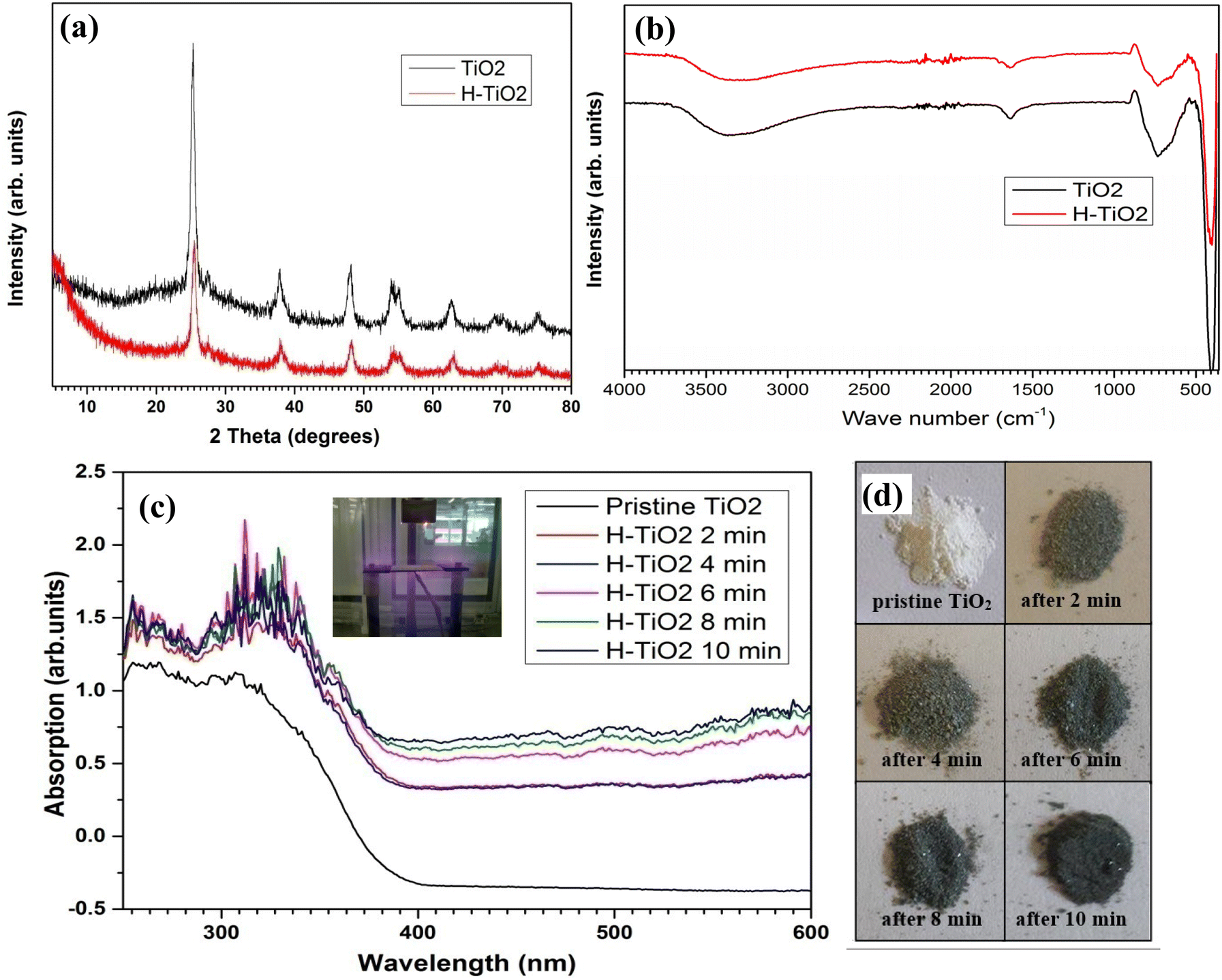 | ||
| Fig. 2 PXRD patterns of (a) FTIR spectra (b) of TiO2 and H plasma treated TiO2 and (c) UV-visible spectra and (d) corresponding photographs of H plasma treated for different exposure time. | ||
FTIR spectra for pristine TiO2 and H-TiO2 are shown in Fig. 2(b). Both pristine TiO2 and H-TiO2 show same IR activity; absorption bands at 3350 cm−1, 1630 cm−1 and 734 cm−1 are due to O–H stretching, O–H bending of surface adsorbed water and Ti–O stretching mode of TiO2 respectively.
Fig. 2(c) shows the UV-Visible absorption spectra for pristine TiO2 and H-TiO2 with different reaction times. It was observed that a significant change in the absorption intensity in the UV region and the absorption in the visible light region gradually increased with extended hydrogenation time. This can be attributed to the colour change in the material, where the white colour of the pristine TiO2 turns into black. The optical absorption characteristics suggest that H plasma treatment introduces surface defect states within the band gap of the TiO2.26–28 Fully black H plasma treated TiO2 sample for 10 min at 500 °C was used for all the other characterisations and nanocomposite formation from here on.
Electron microscopy on hydrogen plasma treated TiO2 nanoparticles
SEM and STEM images for pristine TiO2 and H-TiO2 are shown in Fig. 3. Pristine TiO2 shows spherical morphology with 25 nm average particle size. After hydrogenation, morphology and particle size remain unchanged. However, it was observed H-TiO2 particles are more aggregated compared to pristine TiO2 NPs. | ||
| Fig. 3 SEM (a) and STEM (b) images of TiO2 nanoparticles and SEM (c) and STEM (d) images of H plasma treated TiO2 nanoparticles. | ||
HR TEM images and electron diffraction patterns for pristine TiO2 and H-TiO2 are shown in Fig. 4.
 | ||
| Fig. 4 HR TEM (a) and FFT (b) images of TiO2 nanoparticles and HR TEM (c) and FFT (d) images of H plasma treated TiO2 nanoparticles. | ||
Electron energy loss (EEL), solid state proton NMR, XPS analysis and band gap calculation of hydrogen plasma treated TiO2 nanoparticles
As seen from the well resolved lattice features in Fig. 4(a) and (b), both pristine and H plasma treated TiO2 are highly crystalline and significant differences are not observed in the HR TEM images. However, fast Fourier transform analysis images (FET) of pristine TiO2 contains more and brighter diffraction spots compared to H-TiO2. This is indicative of some distortion in the TiO2 atomic lattice structure lattice after the hydrogenation process and is consistent with optical absorption indication the introduction defect states within the band gap. Furthermore, in Fig. 5(a) the Electron Energy Loss (EEL) spectra for pristine TiO2 and H-TiO2, shows that the peak at 464.8 eV for pristine TiO2 has shifted to 465.8 eV after H plasma treatment. The chemical shift can be due to the change in charge transfer from Ti to O in H plasma treated TiO2. This is further evidence of the chemical changes in the TiO2 surface during hydrogenation via H plasma treatment. The EELS spectrum of pristine TiO2 is in good agreement with previously reported data in the literature. Ti L3,2 edge in TiO2 shows two spectral lines split into two maxima due to crystal field splitting where octahedral coordination of Ti atom with O splits into degenerate 3d states. | ||
| Fig. 5 (a) EEL spectra (b) H-NMR spectra (c) XPS Ti 2p spectra and (d) UV absorption spectra arranged according to the Kubelka–Munk function for H-TiO2 NPs. | ||
H-NMR spectra of pristine TiO2 and H-TiO2 nanoparticles show broad peaks at chemical shifts of 9.3 ppm and 7.6 ppm respectively. However, H-TiO2 nanoparticles shows two small additional peaks at 4.0 ppm 2.4 ppm which could be ascribed the presence of weakly bound hydrogen atoms as a result of the H plasma treatment. The multiplicity of the NMR peaks can be used to identify the number of H environments within the sample. The peaks at 4.0 ppm and 2.4 ppm can be attributed to bridging and terminal titanol groups.29
XPS analysis of Ti 2p region reveals a slight shift of binding energies as shown in Fig. 5(c). The Ti 2p XPS spectra shows two main peaks at 458.4 eV and 463.9 eV due to the spin–orbit pairs of 2p3/2 and 2p1/2. In addition, a satellite peak at 471 eV was observed.31 A similar trend was observed for the Ti 2p in H-TiO2 (2p3/2 peak at 458.6 eV, 2p1/2 peak at 464.3 eV and satellite peak at 472 eV). These slight changes in the binding energies can be attributed to the oxygen vacancy formation in the TiO2 surface. A notable change in the binding energies of O 1s was not observed in agreement with previous studies. HOMO and LUMO energy levels of H plasma treated TiO2 NPs were extracted using UV/Vis Fig. 5(d) and UPS data (Fig. S1†). It was observed that band gap of pristine TiO2 NPs (3.20 eV) has reduced to 3.1 eV following the hydrogenation process which is in agreement with the previous studies.26 HOMO level of energy of pristine TiO2 measured in our previous work was −7.5 eV. H-TiO2 gives a HOMO value of 5.90 eV during the hydrogenation process. This is a very significant shift of 1.6 eV. UPS probes the first 2–3 nm of the surface of the nanoparticles. The NMR shows that the surface of the H-TiO2 has titanol groups. The surface modification through the titanol groups may contribute to the shift in the HOMO energy measured. In addition to above characterisation techniques, elemental analysis for hydrogen was performed on hydrogenated TiO2 samples and it shows that 0.2% of average weight percentage of hydrogen is present. It suggests that TiO2![[thin space (1/6-em)]](https://www.rsc.org/images/entities/char_2009.gif) :H molecular ratio is roughly 5:1. Pristine TiO2 did not give any significant reading.
:H molecular ratio is roughly 5:1. Pristine TiO2 did not give any significant reading.
H-TiO2/CRS nanocomposites and MIM capacitors
 | ||
| Fig. 6 (a) PXRD traces, (b) SEM images cross section of a H-TiO2/CRS (10%) (c) XPS N 1s spectra for CRS and H-TiO2/CRS (d) XPS Ti 2p spectra for H-TiO2 and H-TiO2/CRS (10%) nanocomposite. | ||
X-ray photoelectron spectroscopy of the N 1s peak from the bare CRS polymer and H-TiO2/CRS and Ti 2p peak from bare TiO2 and H-TiO2/CRS are shown in Fig. 6(c). The N 1s spectra for the CRS polymer showed two major peaks with binding energies of 397.4 eV and 397.9 eV whereas, N 1s spectra for the H-TiO2/CRS resolved into three peaks at 400.3 eV, 401.5 eV and 402.5 eV. The shifting of the binding energy of N 1s in the CN group of the polymer confirms the interaction of the CRS polymer with H-TiO2 nanoparticles. In Fig. 6(d) the Ti 2p XPS spectra for H-TiO2 shows two main peaks at 457.2 eV and 462.8 eV due to the spin–orbit pairs of 2p3/2 and 2p1/2. In addition, a satellite peak at 470.4 eV was observed. For H-TiO2/CRS; the Ti 2p3/2 and 2p1/2 peaks are shifted to 461.3 eV and 466.8 eV respectively. However, satellite peak was not observed. A notable change in the binding energies of C 1s and O 1s were not observed. Furthermore, N 1s spectral line of CRS-H-TiO2 has shifted to higher values compared to CRS-TiO2 nanocomposite. This can be ascribed as to the changes that arise in the electronic structure of H-TiO2 during hydrogenation which facilitate the bonding interactions of H-TiO2 with the CRS polymer matrix. The XPS data suggest that the interaction of the CRS with H-TiO2 occurs via interactions of Ti with N to TiN type complexes.30
Electrical properties of H-TiO2/CRS nanocomposites MIM capacitors
The capacitances of the H-TiO2/CRS nanocomposite films and bare CRS polymer were measured in the frequency range from 1 kHz to 1 MHz and are shown together with their respective dielectric constants in Fig. 7(a) and (b). | ||
| Fig. 7 (a) Capacitance and (b) dielectric constant as a function of frequency and capacitance (c) and current densities (d) as a function of voltage for H-TiO2/CRS nanocomposites with different H-TiO2 loadings. | ||
The capacitance values for the bare polymer and 10% weight CRS–H-TiO2 composite remain constant up to 500 kHz and then gradually decreases with increasing frequency. For 20% and 30% weight H-TiO2/CRS composite, capacitance values sharply decrease after 10 kHz with increasing frequency. This behaviour is due to the relaxation process in H-TiO2/CRS interface.31
However, capacitance values for all TiO2/CRS nanocomposites reported in our previous work are stable up to 500 Hz compared to H-TiO2/CRS nanocomposites. This suggests that the addition of H plasma treated TiO2 initiates the relaxation process at lower frequencies compared to pristine TiO2, in the CRS matrix. Which is consistent with the H plasma treatment creating surface defect states deep in the band gap which take longer to fill/empty. Dielectric constants for all three composites were calculated using the average film thickness measured by AFM (Fig. S2†). At 1 kHz CRS–H-TiO2 nanocomposites exhibited high dielectric constants of 80, 118 and 131 with 10%, 20% and 30% weight of H-TiO2 respectively which is significantly higher than of pure CRS. Fig. 7(c) shows capacitance–voltage measurements for all three nanocomposite films and bare CRS polymer and it was observed that capacitance values for all three nanocomposites and bare CRS polymer in the voltage range of −2 V to 2 V are very stable. The leakage current densities are relatively low, in the range of 10−6 A cm−2–10−8 A cm−−2. However, as seen in TiO2/CRS nanocomposites,5 the H-TiO2/CRS current voltage characteristics also possess a distinct asymmetry and a shift in the zero current up to 1 V is seen for composites with different TiO2 loading. This shift in the minimum current from 0 V could be due to the charging of the H-TiO2/CRS interfaces. There is likely to be charging at the contacts when there is a high concentration of NPs >10% in the nanocomposite. Furthermore, all three H-TiO2/CRS nanocomposites show a loss factor <0.3 at 1 kHz (Fig. S3†).
Conductive atomic force microscopy on H-TiO2/CRS nanocomposite films
Fig. 8 shows topography and current AFM images of H-TiO2/CRS nanocomposite films. As shown in Fig. 8(a), H-TiO2 nanoparticles within the polymer gives rise to topology differences. In the AFM topography image bright spots are ascribed to H-TiO2 nanoparticles exposed on the surface. The corresponding current distribution image of H-TiO2/CRS nanocomposite is shown in Fig. 8(b). Fig. 8(c) shows overlap of Fig. 8(a) and (b). In addition, Fig. 8(d–g) shows topography, corresponding C-AFM image of current distribution, topography-current image overlaps and IV curve of selected H-TiO2 agglomerate on the nanocomposite thin film. Fig. 8(h) shows step height of 10% H-TiO2/CRS nanocomposite which was used to measure the average film thickness.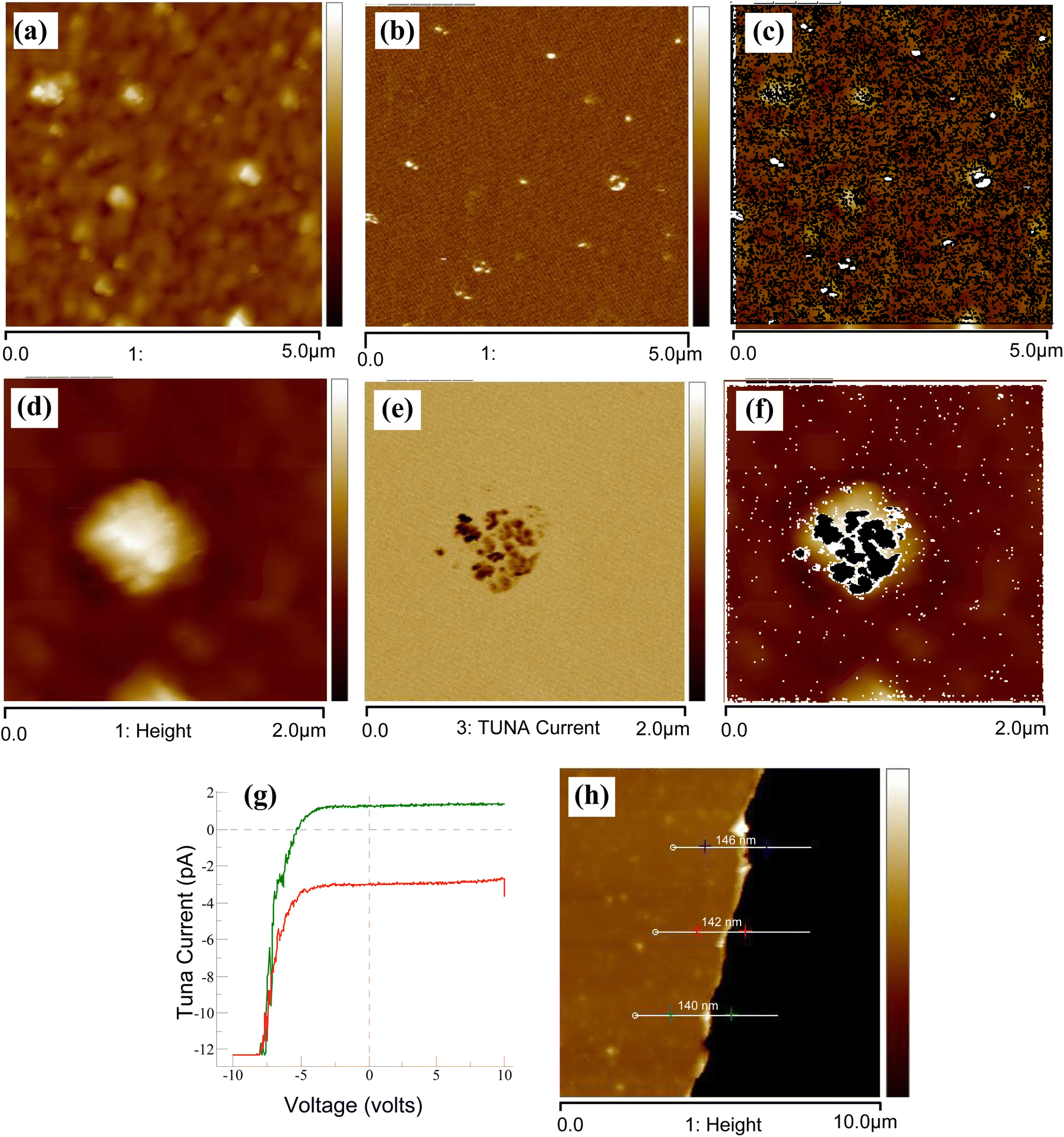 | ||
| Fig. 8 (a) Topography image for H-TiO2/CRS 10% thin film. (b) Current distribution image for H-TiO2/CRS 10% thin film, (c) overlap of topography and current distribution for H-TiO2/CRS 10% thin film. (d) Topography image for selected H-TiO2 agglomerate in H-TiO2/CRS 10% thin film. (e) Current distribution for selected H-TiO2 agglomerate in H-TiO2/CRS 10% thin film. (f) Overlap of topography and current distribution selected H-TiO2 agglomerate in H-TiO2/CRS 10% thin film. (g) IV curve for selected H-TiO2 agglomerate in H-TiO2/CRS 10% thin film. (h) Step height of H-TiO2/CRS 10% thin film. | ||
In the C-AFM configuration the biasing conditions negative currents are measured, corresponding to dark spots in the C-AFM image. The dark spots in the current image are in the vicinity of H-TiO2 particles and leakage paths through the nanocomposite are associated with the H-TiO2 nanoparticles. For a negative potential at the tip, I–V curve shows typical diode type behaviour between the Pt coated AFM tip and the H-TiO2 nanoparticle embedded in CRS polymer.
Energy band diagram for H-TiO2/CRS
Energy band diagram for H-TiO2 and CRS interface was constructed using the HOMO and LUMO energy levels of H-TiO2 and pristine CRS polymer extracted using UV/Vis and UPS data as discussed in detail previously in ref. 20. Same as in CRS–TiO2 system, band energy levels for CRS are aligned to those of H-TiO2 as shown in Fig. 9 below. | ||
| Fig. 9 Energy band diagram for H-TiO2/CRS nanocomposite. | ||
Though the CRS is an insulator, at the interface with the H-TiO2 it is shown as having the capability to charge through interaction with defect and polarised bonding states. The interface at equilibrium therefore conforms to a semiconductor heterojunction model. However, when a potential is applied at the terminals and there is a shift from the equilibrium, only states on the H-TiO2 side of the interface are available for further filling or emptying. The equilibrium situation is taken as frozen-in charge at the interface. Therefore, the CRS acts as an insulator (no charge) away from the interface, while the charge on the H-TiO2 side of the interface can change. It is this additional charge which has to be balanced at the terminals of the composite dielectric which leads to the increase in the overall relative permittivity of the nanocomposite film.
Surface modification of NPs was used to improve the chemical interactions at the interfaces between nanoparticles and polymer matrix and thereby influence the charge transfer at the interface to tailor the dielectric properties of the nanocomposites. Hydrogenated TiO2 nanoparticles obtained by H plasma treatments of pristine confirmed the presence titanol type functionality on TiO2 NPs and the surface amorphous nature H-TiO2. The pristine TiO2 NPs with CRS polymer show higher energy densities (At 1 kHz, 80, 118 and 131 dielectric constants extracted were for H-TiO2/CRS nanocomposites with 10%, 20% and 30% weight of H-TiO2 respectively. In the case of TiO2/CRS nanocomposites dielectric constants were 118, 176 and 207 with 10%, 20% and 30% weight of TiO2 respectively). In the case of H-TiO2, introduction of titanol type functionality on the TiO2 surface improves the bonding interactions at the polymer–nanoparticles interface resulting reduced structural mobility. Thus, charging of the interface due to defects from unpaired bond is inhibited. However, capacitance values for H-TiO2/CRS nanocomposites in the voltage range of −2 V to 2 V are very stable compared to pristine TiO2 and CRS nanocomposite. In traditional dielectric composites the highest dielectric constant that can be achieved is always found to be below the dielectric constant of the filler as explained by the logarithmic mixing rule. However, it has been shown that with the introduction of nanosized fillers into polymer matrices significantly higher dielectric constants compared to that of the filler could be achieved. Two models have been proposed to explain this behaviour, one termed the interface model10 and the other the multi core model.32 According to the interface model, the interface zone between the nanoparticle and the polymer has a vital influence on the properties of the dielectric as whole. In the multicore model, dielectric nanoparticles dispersed in a polymer matrix are assumed to result in the formation of different layers termed the bound layer, intermediate layer and the loose layer. The bound layer (1st layer) corresponds to the nanoparticle and polymer bonding through functional groups to form an interface which is responsible for the formation of the diffuse electrical double layer. The intermediate layer (2nd layer) consists of polymer chains strongly bonded to the bound layer. The loose layer (3rd layer) is a region of polymer loosely bound to the second layer. The polarisation phenomena occurring in the interface zones of nanoparticles are proposed as being responsible for ultra-high dielectric constants measured in these dielectric nanocomposites. We propose an extension of this model based on the nanoparticle being a semiconductor which can be internally charge depleted/accumulated to give an increase in the effective dielectric permittivity (constant).
Conclusions
CRS–H-TiO2 nanocomposites which exhibit ultra-high dielectric constants 80, 118 and 131 for nanocomposites with 10%, 20% and 30% weight of hydrogenated TiO2 respectively, significantly higher than values of pure CRS (21) and TiO2 (41). Furthermore, all three CRS-hydrogenated TiO2 nanocomposites show a loss factor <0.3 at 1 kHz and low leakage current densities (10−6 A cm−2–10−7 A cm−2). It was observed that the low leakage current is associated with hydrogenated TiO2 nanoparticles embedded in the CRS polymer matrix. Although, modified interface slightly reduces energy densities compared to the pristineTiO2/CRS system, it increases the stability of capacitance values for H-TiO2/CRS in the voltage range of −2 V to 2 V compared to pristine TiO2/CRS. The results show that the polymer–nanoparticle interface plays a major role in tuning dielectric properties of the nanocomposite as per the interface model. Also, it was observed that HOMO–LUMO energy alignments between CRS and H-TiO2 also enhance the polarisation of the nanoscale interfaces which are distributed within the dielectric. The dielectric behavior of nanoscale inorganic dielectrics dispersed in a high permittivity polymer can be tuned via modification of the surface properties of inorganic dielectric nanoparticles employing solution free techniques such as hydrogen plasma treatments to obtain electrically stable nanocomposite dielectrics for high energy density capacitors.Conflicts of interest
There are no conflicts to declare.Acknowledgements
This work was supported by Dyson Research Ltd. NA is also grateful to the Cambridge Commonwealth Trust for financial support and Prof. William Jones, Department of Chemistry, University of Cambridge for providing wet chemical laboratory facilities. Sri Lanka Institute of Nanotechnology (SLINTEC) is acknowledged for providing TEM and solid-state NMR facilities. NA further acknowledges Dr Nuwan de Silva and Dr Dinara Gunasekera for ss-NMR data collection.References
- A. P. Arico, P. Bruce, B. Scrosati, J. M. Tarascon and W. V. Schalkwijk, Nat. Mater., 2005, 4, 366–377 CrossRef CAS PubMed.
- G. Yu, X. Xie, L. Pan, Z. Bao and Y. Cui, Nano Energy, 2013, 2, 213–234 CrossRef CAS.
- H. P. Palani, V. Shanmugasundram, E. Jayamani and K. H. Soon, Renewable Sustainable Energy Rev., 2022, 157, 12075 Search PubMed.
- J. C. Pandey and M. Singh, SPE Polym., 2021, 2, 236–256 CrossRef.
- M. S. Whittingham, MRS Bull., 2008, 33, 411–419 CrossRef CAS.
- S. P. Culver, C. W. Beier, J. P. Rafson and R. L. Brutchey, J. Appl. Polym. Sci., 2014, 131, 40290 CrossRef.
- W. Wu, T. Liu, D. Zhang, Q. Sun, K. Cao, J. Zha, Y. Lu, B. Wang, X. Cao, Y. Feng, V. A. L. Roy and R. K. Y. Li, Composites, Part A, 2019, 127, 105650 CrossRef CAS.
- J. J. Xu, C. Fu, H. Chu, X. Wu, Z. Tan, J. Qian, W. Li, Z. Song, X. Ran and W. Ni, Sci. Rep., 2020, 10, 17084 CrossRef CAS.
- D. Khastgir, H. S. Maiti and P. C. Bandyopadhyay, Mat. Sci. and Eng., 1988, 100, 245–253 CrossRef CAS.
- T. J. Lewis, Trans. IEEE, 1994, 1, 812–825 CAS.
- J. K. Nelson, J. C. Fothergill and L. A. Dissado, Annu Rep IEEE Conf Electr Insul Dielectr Phen: 295–298.
- F. C. Chen, C. W. Chu, J. He, Y. Yang and J. L. Lin, Appl. Phys. Lett., 2004, 85, 3295–3298 CrossRef CAS.
- J. K. Nelson and J. C. Fothergill, Nanotechnology, 2004, 15, 586–595 CrossRef CAS.
- A. Maliakal, H. Katz, P. M. Cotts, S. Subramoney and P. Mirau, J. Am. Chem. Soc., 2005, 127, 14655–14662 CrossRef CAS.
- R. R. Prakash, S. Pandiarajan, P. Venkatesh and N. Kamaraj, IEEE, 2011, 978, 46–49S Search PubMed.
- J. Li, S. Seok, B. Chu, F. Dogan, Q. Zhang and G. Wang, Adv. Mater., 2009, 21, 217–221 CrossRef CAS.
- A. Shubha, S. R. Manohara and B. Angadi, Polym. Bull., 2022, 79, 7117–7135 CrossRef CAS.
- H. Rekik, Z. Ghallabi, I. Royaud, M. Arous, G. Seytre, G. Boiteux and A. Kallel, Composites, Part B, 2013, 45, 1199–1206 CrossRef CAS.
- J. Kim, S. H. Lim and Y. S. Kim, J. Am. Chem. Soc., 2010, 132, 14721–14723 CrossRef CAS.
- N. Madusanka, S. G. Shivareddy, P. Hiralal, M. D. Eddleston, Y. Choi, R. A. Oliver and G. A. J. Amaratunga, Nanotechnology, 2016, 27, 195402 CrossRef PubMed.
- C. K. Chiang and R. Popielarz, Ferroelectrics, 2002, 275, 1–9 CrossRef CAS.
- N. Madusanka, S. G. Shivareddy, M. D. Eddleston, R. A. Oliver and G. A. J. Amaratunga, Carbohydr. Polym., 2017, 172, 315–321 CrossRef CAS.
- H. He, K. Yang, N. Wang, F. Luo and H. Chen, J. Appl. Phys., 2013, 114, 213505-5 Search PubMed.
- T. Leshuk, R. Parviz, P. Everett, H. Krishnakumar, R. A. Varin and F. Gu, ACS Appl. Mater. Interfaces, 2013, 5, 1892–1895 CrossRef CAS.
- X. Lu, G. Wang, T. Zhai, M. Yu, J. Gan, Y. Tong and Y. Li, Nano Lett., 2012, 12, 1690–1696 CrossRef CAS.
- Y. Yan, M. Han, A. Konkin, T. Koppe, D. Wang, T. Andreu, G. Chen, U. Vetter, J. R. Morante and F. Schaa, J. Mater. Chem. A, 2014, 2, 12708–12716 RSC.
- G. Yang, Z. Jiang, H. Shi, T. Xiao and Z. Yan, J. Mater. Chem., 2010, 65(20), 5301 RSC.
- Y. Sun, Z. Sun, S. Gao, H. Cheng, Q. Liu, J. Piao, T. Yao, C. Wu, S. Hu, S. Wei and Y. Xie, Nat. Commun., 2012, 3, 1057 CrossRef.
- M. Mehta, N. Kodan, S. Kumar, A. Kaushal, L. Mayrhofer, M. Walter, M. Moseler, A. Dey, S. Krishnamurthy, S. Basu and A. P. Singh, J. Mater. Chem. A, 2016, 4, 2670–2681 RSC.
- S. A. Bakar and C. Ribeiro, J. Photochem. Photobiol., C, 2016, 27, 1–29 CrossRef.
- A. K. Jonscher, J. Phys. D: Appl. Phys., 1999, 32, R57–R70 CrossRef CAS.
- T. Tanaka, M. Kozaroko, N. Fuse and Y. Ohki, IEEE Trans. Dielectr. Electr. Insul., 2005, 12, 187–196 Search PubMed.
Footnote |
| † Electronic supplementary information (ESI) available. See DOI: https://doi.org/10.1039/d2nr04680f |
| This journal is © The Royal Society of Chemistry 2023 |