
 Open Access Article
 This Open Access Article is licensed under a
 Creative Commons Attribution 3.0 Unported Licence
Exploiting flux shadowing for strain and bending engineering in core–shell nanowires
Mahmoud
Al Humaidi
 *abc,
Julian
Jakob
ab,
Ali
Al Hassan
bc,
Arman
Davtyan
c,
Philipp
Schroth
abc,
Ludwig
Feigl
b,
Jesús
Herranz
d,
Dmitri
Novikov
e,
Lutz
Geelhaar
d,
Tilo
Baumbach
ab and
Ullrich
Pietsch
c
*abc,
Julian
Jakob
ab,
Ali
Al Hassan
bc,
Arman
Davtyan
c,
Philipp
Schroth
abc,
Ludwig
Feigl
b,
Jesús
Herranz
d,
Dmitri
Novikov
e,
Lutz
Geelhaar
d,
Tilo
Baumbach
ab and
Ullrich
Pietsch
c
aLaboratory for Applications of Synchrotron Radiation, Karlsruhe Institute of Technology, Kaiserstraße 12, D-76131 Karlsruhe, Germany. E-mail: mahmoud.humaidi@kit.edu
bInstitute for Photon Science and Synchrotron Radiation, Karlsruhe Institute of Technology, Hermann-von-Helmholtz-Platz 1, D-76344 Eggenstein-Leopoldshafen, Germany
cSolid State Physics, Emmy-Noether Campus, Walter-Flex Straße 3, D-57068 Siegen, Germany
dPaul-Drude-Institut für Festkörperelektronik, Leibniz-Institut im Forschungsverbund Berlin e.V., Hausvogteiplatz 5-7, D-10117 Berlin, Germany
eDeutsches Elektronen-Synchrotron, PETRA III, D-22607 Hamburg, Germany
First published on 2nd November 2022
Abstract
Here we report on the non-uniform shell growth of InxGa1−xAs on the GaAs nanowire (NW) core by molecular beam epitaxy (MBE). The growth was realized on pre-patterned silicon substrates with the pitch size (p) ranging from 0.1 μm to 10 μm. Considering the preferable bending direction with respect to the MBE cells as well as the layout of the substrate pattern, we were able to modify the strain distribution along the NW growth axis and the subsequent bending profile. For NW arrays with a high number density, the obtained bending profile of the NWs is composed of straight (barely-strained) and bent (strained) segments with different lengths which depend on the pitch size. A precise control of the bent and straight NW segment length provides a method to design NW based devices with length selective strain distribution.
1. Introduction
Due to their large surface to volume ratio, NWs have size-dependent mechanical properties allowing for strain engineering.1–3 Strain engineering can be used to tune the electronic band gap and to tailor the performance of NW-based devices.4–6 Additionally, piezoelectric fields in strained NWs can be used for efficient carrier sweeping toward device electrodes.7–9 Therefore, strained heteroepitaxial core–shell NWs formed from lattice-mismatched materials have potential applications in NW-based devices such as light-emitting diodes,10,11 solar cells,12–15 and electronic devices.16 As a consequence of the elastic release of interface strain, thin NWs bend if a heteroepitaxial shell is grown inhomogeneously on their perimeter.17–19 In the case of the growth of a shell with a higher lattice parameter compared to the core, the strain gradient across the NW diameter varies from tensile strain at the shell surface towards compressive strain at the opposite side.20–22 Due to the impact of deformation potentials on the band structure, the strain gradient across the bent NW induces a drift in the charge carriers toward the regions with tensile strain which allows tuning of the electronic properties of the NWs for future optoelectronic devices. Moreover, bent NWs can be used for NW networks or interconnects for electronics with novel designs.16 Lewis et al.20 reported on NW bending induced by growing a non-uniform Al0.5In0.5As shell (≈3.6% lattice mismatch) on GaAs NW cores. The non-uniformity of the shell growth in this case was achieved by sequential NW rotation and shell deposition and resulted in shell growth on defined NW sides. Recently, we have reported on non-uniform InxGa1−xAs shell growth by MBE deposition on the GaAs NW core without substrate rotation where the shell was grown mainly on NW side walls defined by a certain flux direction of the growth materials.23 By controlling the core diameter, d, shell thickness, t, and alloy concentration, x, in the shell, it was possible to manipulate the curvature of the NW. However, the NW growth reported in ref. 20 and 23 was performed on a silicon substrate with a low number density resulting in homogeneous bending of all NWs along the entire length. In this work, we report on GaAs NW growth on pre-patterned Si(111) substrates followed by a lattice mismatched InxGa1−xAs shell growth without substrate rotation. To control the axial distribution of the shell material along the NWs, we benefit from the well-defined NW height and pattern with respect to the MBE geometry. We exploit the shadowing of the material fluxes by neighboring NWs and consequently a varying strain distribution along the NW and different bending profiles are obtained. Our findings are observed by in situ X-ray diffraction (XRD) measurements performed using NW arrays with different pitch sizes (i.e. different number densities of the NWs) during shell growth.2. The fundamental idea
In this study, we used two samples (denoted as sample-1 and sample-2 in the text) of NW arrays where the separation between neighboring NWs (pitch p) on patterned arrays varies from p = 0.1 μm to 10 μm. Shell growth for sample-1 was intended to induce higher NW bending compared to sample-2. Sample-1 was observed by scanning electron microscopy (SEM) while sample-2 was monitored by in situ XRD during shell growth. For the growth of the NW core and the shell, we used a portable MBE chamber that is equipped with Ga and In effusion cells and an As4 valve cracker cell as shown in Fig. 1(a). Considering the substrate area around an individual NW, the decrement in p associated with the shadowing of the Ga-flux by neighboring NWs results in the growth of shorter and thinner NWs compared to the ones grown with larger p (lower density).24–28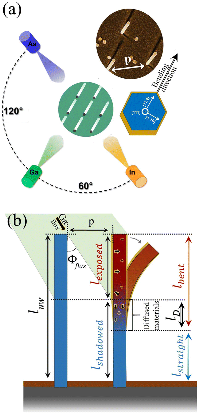 | ||
| Fig. 1 (a) Illustration of the azimuthal arrangement of the MBE cells and the pattern of the substrate. (b) Illustration of material flux shadowing by neighboring NWs. | ||
An observed influence of the cell arrangement of the same MBE chamber on the bending direction of the NWs was reported in ref. 23. It was observed that NWs grown on patterned Si substrates with the given growth parameters bend toward the direction of the Ga flux in the case of performing no substrate rotation during shell growth. The predetermination of the bending direction and the geometrical arrangement of the pMBE effusion cells with respect to the NW arrays are illustrated schematically in Fig. 1(a).
The exploited flux shadowing of the shell growth material by neighboring NWs and the resulting bending profile of the NW are demonstrated in Fig. 1(b). The NW arrays with high number density experience prominent flux shadowing and display a lower straight (shadowed) segment and an upper bent (exposed) segment of the NW. The length ratio of the exposed (lexposed) and the shadowed (lshadowed) NW segments can be controlled by changing the flux angle (Φflux), the NW length (l) and the distance (p) as shown in Fig. 1(b). Therefore, the length of (lexposed) is given by
 | (1) |
For the length of the bent segment lbent, the diffusion of the shell materials on the NW surface from the exposed part toward the shadowed part of the NW must be considered. Therefore,
| lbent = lexposed + lD | (2) |
The length lD indicates the effective diffusivity of group-III materials on the NW surface that accumulate and cause strain-induced NW bending. Fig. 2(a) shows exemplary 30° tilt view SEM images of reference GaAs NWs in arrays with p = 100, 200, 400 and 700 nm, evidencing high NW yield. As shown in Fig. 2(b), 30° title view SEM images are taken from four NW arrays of sample-1 with different p showing significant variations in the NW bending profiles after shell growth implying a varying strain distribution along these NWs. For the NW arrays with p = 100 and 200 nm, the bending occurs at the upper part of the NW which appears thicker in diameter compared to the straight lower part due to the shadowing effect on the latter.
 | ||
| Fig. 2 (a) The 30° tilt view SEM images of the reference GaAs NW arrays with different pitch size p values before shell growth. (b) The 30° tilt view SEM images of bent GaAs–In0.3Ga0.7As core–shell NWs in arrays with different pitch size p values (sample-1) (scale bars correspond to 500 nm). | ||
3. Results and discussion
During the increment of the shell thickness the axial component of the lattice mismatch strain ε∥ increases which in turn exerts a stronger bending force on the NW core.In order to get deeper insights into the evolution of the bending and the strain along the NWs in different arrays, we performed an in situ XRD experiment. By scanning the sample across the X-ray beam while fulfilling Bragg's condition of the GaAs(111) reflection, the micro-fields of NWs were precisely located with respect to the diffractometer geometry. For each field with a particular p value, we monitored the evolution of NW bending as a function of the In0.15Ga0.85As shell growth time for sample-2. Fig. 3(a) shows the 3D distribution of the GaAs(111) Bragg reflection in a reciprocal space map (RSM) of the NW arrays with p = 100, 200 and 400 nm acquired from the in situ XRD measurement. These maps are recorded at different times of In0.15Ga0.85As shell growth for sample-2. The recorded 3D RSMs shown in Fig. 3(a) are represented by the reciprocal space vectors Qx, Qy and Qz, where Qz is set parallel to the GaAs[111] NW growth axis and sensitive to the axial strain ε∥ while Qx and Qy are parallel to the Si(111) plane of the substrate and sensitive to the changes in the crystal orientation (i.e. tilting and bending of the NW). In addition to these vectors, we introduce two new vectors, Q and Qr where Q is set along the bending direction of the QxQy component of the RSM as demonstrated by the blue arrow in Fig. 3(a). The other vector Qr has the same origin as the other vectors but is tilted from Qz by a bending angle of the NW crystal. The lower images in Fig. 3(a) are of the RSMs of straight GaAs NWs at different arrays and the top images are that of the NWs after 20 minutes of shell growth where 2D cross-sections are highlighted along the bending direction.
 | ||
| Fig. 3 (a) 3D RSMs of the GaAs(111) Bragg's reflection after different shell growth rounds stacked vertically for NW arrays with p = 100, 200 and 400 nm. (b) Integrated line profile of the intensity distribution of the XRD signal along Q in RSM. | ||
3.1. Bending profile of the NW
The recorded RSMs in Fig. 3(a) show that for the arrays with p = 100 and 200 nm the most intense part of the Bragg's reflection is located close to Q = 0 Å−1 with some broadening toward higher Q values. This finding implies that a large section of the lower part of the NWs remain straight and perpendicular to the substrate surface, while the broadening reflects the bending section of the upper part of the NW. In contrast to the arrays with p = 400 nm, the peaks exhibit a rather homogeneous broadening toward higher Q values indicating that the whole NW bends.The integrated intensity profiles of Bragg peaks along Q for the arrays with p = 100, 200 and 400 nm are plotted in Fig. 3(b). It can be seen that the intensity of the integrated line profiles depends on the number density of the NWs for different arrays. For arrays with p = 100 and 200 nm, the evolution of the Bragg peak profile along Q shows that the peak maxima decreases and a peak tailing evolves indicating an increasing NW curvature on the exposed parts of the NW. To quantify the signal profiles, we first introduce the symmetry factor S (also known as the tailing factor) of each Bragg peak along Q by
 | (3) |
 | ||
| Fig. 4 (a) The calculated symmetry factor S of the line profiles of the GaAs(111) NW Bragg peaks for different NW arrays, integrated along Q in RSM as a function of shell growth time. (b) The relative changes of the maximum intensities of the Bragg peaks of the NWs on different arrays as a function of shell growth time. (c) Exemplary plots of the multi-Gaussian fitting model used to deconvolute the integrated line profiles of the Bragg peak of the NWs at the arrays with p = 100 nm. (d) Estimated length of the NW segments that exhibited bending extracted from the XRD peak profile and compared to the length of the exposed segment indicating the length of the NW segment that is covered by the diffused materials (lD). (e) The peak position of the XRD signal of the lower part of the NW at the arrays with p = 100 and 200 nm as a function of shell growth time (the blue and red shades indicate the corresponding uncertainty range of the peak position acquired from the fitting model). | ||
As the NW curvature increases, the maximum intensity of the Bragg peak decreases due to the spreading of the diffracted signal distribution along Q that results from the changes in crystal orientation along the bent NW. The contribution of the straight part appears as an intense peak located closely to Q = 0 Å−1 in the RSM while the bent part appears as a tailing of the diffraction peak along the bending direction as shown in Fig. 3. As the length of the bent part increases, the tailing of the diffraction signal increases. Therefore, the signal of the arrays with p = 200 nm has a lower symmetry compared to the arrays with p = 100 nm as shown in Fig. 4(a).
Furthermore, Fig. 4(b) shows the relative changes in the Bragg peak maximum intensity at different shell growth times. The maxima of the Bragg peak of bare GaAs NW drops to ≈20% after 20 minutes of shell growth at the arrays with p = 400 and 700 nm. Whilst the maxima of the Bragg peak intensity profile of the NW arrays with p = 100 and 200 nm decrease to ≈45% and ≈25%, respectively. These values indicate the percentage of the diffracted signals from the NWs that accumulate at the same position in the RSM for these two arrays. Therefore, approximately 45% and 25% of the NW volume remains vertical to the substrate surface for the NW arrays with p = 100 and 200 nm, respectively. To innervate this approach, the Bragg peak profiles of the NW at these arrays were deconvoluted by multiple-Gaussians as shown in Fig. 4(c). By integrating the area of each Gaussian, this model gives the same percentages of the XRD signal that remained close to Q = 0 Å−1 in RSM for the two mentioned arrays shown before (shaded with blue in Fig. 4(c)).
Accordingly, the average volume of the NW part that exhibits bending forms about 55% and 75% of the total volume of the NWs at the arrays with p = 100 and 200 nm, respectively.
The length lexposed of the NW can be calculated from eqn (1) as listed in Table 1 by considering the distance between the NWs which is √3p in our case as the shadowing in sample-2 is done by the next neighboring NWs.
| Pitch size (p) [nm] | l average [nm] | l exposed [nm] |
|---|---|---|
| 100 | 850 ± 90 | 320 |
| 200 | 1035 ± 70 | 652 |
| 400 | 1120 ± 50 | 1120 |
| 700 | 1150 ± 50 | 1150 |
| 1000 | 1150 ± 50 | 1150 |
By considering that the average length of the NWs is lpaverage for the mentioned arrays, the length of the bent part lpbent can be calculated as l100bent = 0.55 × l100average = 468 nm and l200bent = 0.75 × l200average = 776 nm. The values of laverage, lbent and lexposed are plotted in Fig. 4(d). From these values, one can estimate the length of the NW segment lpD that is covered by the diffused shell materials by l100D = l100bent − l100exposed ≈ 142 nm and l200D = l200bent − l200exposed ≈ 124 nm, therefore, laverageD ≈ 135 nm.
However, the length lD depends on the diffusivity of the shell materials which in turn depends on the NW surface properties and the shell growth parameters. Therefore, lD is valid for the given parameters of the shell growth of the studied sample and may be changed by changing these parameters.
Fig. 4(e) shows the position of the Bragg peak maxima on Q of the arrays with p = 100 and 200 nm as the function of shell growth time. It can be seen that the peak position exhibited minor changes during the first 5 minutes of shell growth indicating a small NW bending of ≈0.025°, under the consideration of the angular resolution of our measurement being limited to 0.01° by the XRD setup. However, these minor changes indicate a minor development of strain and curvature in the entire NW at the beginning of shell growth. This might be explained by the high diffusivity of the shell material at the early stages of shell growth which may decrease the shell thickness and strain due to the NW surface increase.
3.2. Strain distribution along the NW
Benefiting from the spatial distribution of the XRD signal in the reciprocal space of the bent NW, we are able to measure the average strain at different parts of the NW during shell growth. By profiling the XRD signal along Qz and Qr at different positions on Q determined from the multiple-Gaussian fitting shown in Fig. 4(c) for the arrays with p = 100 nm and p = 200 nm, the line profiles along Qz are taken at Q ≈ 0 Å−1 of the GaAs(111) XRD signal at different NW arrays (indicated by blue lines in Fig. 5(a)). At this position in the RSM, the diffracted signal from the lowest part of the NW (i.e. NW bottom, we denote it in the text as B) occurs. To evaluate the strain at the middle segment (denoted by M) of the bent part of the NW, we integrated the line profiles along Qr for each recorded RSM. The line profile along Qr is taken at the peak shoulder along Q in the case of the arrays with p = 100 nm and p = 200 nm, and at the peak center for the arrays with p = 400 nm and p = 700 nm as indicated by black lines in Fig. 5(a). | ||
| Fig. 5 (a) 2D section of the XRD peak of GaAs(111) in RSM on QQz of the arrays with p = 100 nm and p = 700 nm of the bare NWs and after 20 minutes of shell growth where the B, M and T labeled arrows indicate the positions of the line profiles along Qr used for strain calculation. (b) The extracted average strain values indicated by symbols and the strain variation indicated by the shaded area at different positions along the NW plotted as a function of shell growth time. (c) Illustration of the strain distribution along the NW and the corresponding positions of B, M and T and the volume of the lower NW part and the volume of the segment that may be included in the overlapping of the XRD signal when integrating a line profile at B. | ||
By considering the distribution of the zinc blende (ZB) and wurtzite (WZ) structures along the grown GaAs NWs, the strain at the top part of the NW (denoted by T) could be evaluated. For the ZB phase dominating NWs, WZ appears at the top and the bottom of the NW due to the changes in the growth conditions during the axial growth of the NWs as reported in ref. 23. Therefore, we integrate a line profile along Qr at the position of the displaced WZ peak on Q for the arrays with p = 400 nm and p = 700 nm while we consider the peak tail on Q for the arrays with p = 100 nm and p = 200 nm as indicated by the red arrows in Fig. 5(a).
The obtained average strain ε∥ is measured from the peak position on Qr or Qz and the strain variation Δε∥ is obtained from the peak broadening on the same vectors as explained in detail in ref. 23 by the following formulas
 | (4) |
 | (5) |
• In the lower part B of the NW, the average strain εB,p∥ in the NWs of the arrays with p = 100 nm increases and saturates at εB,100∥ = 0.0007 after 16 minutes of shell growth, while εB,200∥ increases in a nonlinear fashion and reaches a value of εB,200∥ = 0.001 after 20 minutes of shell growth as shown in the left panel of Fig. 5(b). This approach indicates the low strain magnitude at the lower parts of the NWs where the shadowing effect takes place. However, the minor strain that built up in the shadowed part of the NWs in these arrays in logical consistency with the observation of the slight bending as shown in Fig. 4(e). In this case, the entire NW during the first few minutes of shell growth is slightly strained due to the high diffusivity of the shell material on the NW surface where this diffusivity decreases as the strain increases. The same approach explains the saturated strain variation as shaded in blue in the left panel of Fig. 5(b). In addition, an overlapping of the signal in the RSM of the bent (strained) part of the NW with the lower (barely-strained) part must be considered as a contributor to the strain curve plotted at these arrays. The volume of the segments that contribute to the overlapping is demonstrated by the red rectangle in Fig. 5(c) and denoted by V2, where V1 is the volume of the straight part of the NW. As the NW curvature increases, the XRD signal from the entire NW spreads more along Q in the RSM and the overlapping of the signals from the different NW segments decreases; therefore,  decreases. The ratio
  explains the relatively higher strain values at B of the arrays when p = 200 nm compared to the ones of arrays with p = 100 nm, where V1 forms 25% of the NW volume at the array with p = 200 nm compared to 45% for the ones with p = 100 nm as shown above.
For the NW arrays with p = 400 nm and p = 700 nm, the average strain increases in the same manner for both NW arrays and reaches a value of εB,400∥ = εB,700∥ = 0.0019 after 20 minutes of shell growth. The strain variations of these arrays increase as the shell growth proceeds as indicated by the green shade in the left panel of Fig. 5(b). However, it was reported in the literature that the strain magnitude at the NW base near the wire–substrate interface is relatively low compared to the other parts of the NW.29,30 This feature at the NW base explains the curve shape of the strain function of the arrays with p = 400 nm and p = 700 nm plotted in the left panel of Fig. 5(b). The same feature explains the higher strain variation at B for the same arrays compared to the other parts M and T that are shaded in green in Fig. 5(b) by the same concept of the overlapping signals in RSMs.
• At position M on the NW, the average strain magnitude of all NW arrays increases to εM,200∥ = εM,400∥ = εM,700∥ = 0.0024 while εM,100∥ = 0.0022 as the shell growth proceeds and the strain variation as it can be seen in the middle panel of Fig. 5(b). This implies a progressive strain evolution and an increasing asymmetry degree of the shell growth around the NW at the parts where no flux shadowing takes place.
• At position T at the NW top, the strain increases as a quadratic function to the shell growth time and reaches a higher value compared to the strain at M where εM,100∥ = 0.0026, εM,200∥ = 0.003 and nM,400∥ = εM,700∥ = 0.0031 as it can be seen in the right panel of Fig. 5(b). This increment of the strain may be explained by the changes in the local deposition geometry of the shell growth material along the NW. As the NW curves, the angle of the incident flux changes along the NW as demonstrated in ref. 31 which leads to an inhomogeneous shell thickness along the exposed segment of the NW. However, in our study, we relate to the early stages of NW bending and the maximum bending angle does not exceed 5° at the NW tip; therefore, the variations in the strain magnitude at B, M and T would increase as the NW bending increases.
4. Methods
4.1. Sample preparation
The shell growth rate and the substrate temperature for both samples were ≈0.8 nm min−1 and 400 °C, respectively. The the In content of sample-1 was x = 0.3 and the shell growth time was 30 minutes. During shell growth, sample-1 was azimuthally aligned in a way that the flux of the shell materials was shadowed by the nearest neighboring NWs (i.e. the distance between the NWs on the bending direction is p). Sample-2 was grown with a lower In content (x = 0.15) and a shell growth time of 20 minutes, resulting in a lower bending compared to that of sample-1. The shadowing in sample-2 is done by the next neighboring NWs (i.e. the distance between the NWs along the bending direction is √3p where the array pattern has a hexagonal grid). The shell growth for sample-2 was realized in several steps as we deposited the shell material for certain time intervals, followed by an interruption of the growth in which the XRD experiment is performed.4.2. XRD measurement and RSM vectors
In order to get deeper insights into the evolution of the bending and the strain along the NWs on different arrays, we performed an in situ XRD experiment. By scanning the sample across the X-ray beam while fulfilling Bragg's condition of the GaAs(111) reflection, the micro-fields of NWs were precisely located with respect to the diffractometer geometry. For each field with a particular p value, we monitored the evolution of NW bending as a function of In0.15Ga0.85As shell growth time for sample-2. The recorded 3D RSMs shown in Fig. 3(a) are represented by the reciprocal space vectors Qx, Qy and Qz, where Qz is set parallel to the GaAs[111] NW growth axis and sensitive to the axial strain ε∥ while Qx and Qy are parallel to the Si(111) plane of the substrate and sensitive to the changes in the crystal orientation (i.e. tilting and bending of the NW). In addition to these vectors, we introduce two new vectors, Q and Qr, where Q is set along the bending direction of the QxQy component of the RSM as demonstrated by the blue arrow in Fig. 3(a). The other vector Qr has the same origin as the other vectors and is tilted from Qz by the bending angle of the NW crystal.5. Conclusion
In this work, we employed the knowledge about the preferable bending direction of the NWs with respect to the azimuthal arrangement of the MBE cells as well as the pitch size to control the shell material distribution along the NWs on different arrays. The strain distribution and the subsequent bending profile of the NWs were different on different NW arrays with different densities. On arrays with high NW densities, the shell materials are deposited asymmetrically on the NW part that is exposed to the direct flux. The diffusion of the shell material toward the shadowed part of the NW was considered and the whole mechanism results in a strained and bent upper part, while the lower part remains rather straight and barely strained.From these NW arrays, we could estimate the length of the NW segment that is strained by the diffused shell materials by means of in situ X-ray diffraction. Additionally, we observed that the shadowed part of the NW exhibits a low strain magnitude and minor bending during the early stages of shell growth, indicating the high diffusivity of the shell materials at the beginning. On the NW arrays with low densities where the shadowing effect does not take place, the shell materials cover the whole length of the NW. On these arrays, the entire NW exhibits bending and the XRD measurement revealed that the strain evolves in the same manner at different parts of the NW. These results provide a method for controlling the NW geometry with novel designs which might be used for NW interconnects as well as tuning the strain distribution along the NWs.
Conflicts of interest
There are no conflicts to declare.Acknowledgements
The authors thank B. Krause, A. Weisshardt, J. Kalt and S. Stankov for their support at KIT, as well as the INT for access to the SEM. We acknowledge DESY (Hamburg, Germany), a member of the Helmholtz Association HGF, for the provision of experimental facilities. Parts of this research were carried out at PETRA III and we would like to thank A. Khadiev for help with the in situ X-ray diffraction and imaging beamline P23 and M. Lippmann for help in the Clean Room. Other parts of this research were carried out at the DESYNanolab and we would like to thank T. F. Keller, A. and S. Kulkani for using the SEM. We are grateful to O. Krüger and M. Matalla (Ferdinand-Braun-Institute, Berlin) for electron beam lithography and to A. Tahraoui, S. Meister and S. Rauwerdink (Paul-Drude-Institut, Berlin) for substrate preparation. This work was funded by the BMBF project 05K16PSA with additional support within the framework of the project MILAS.References
- M. Nasr Esfahani and B. E. Alaca, Adv. Eng. Mater., 2019, 21, 1900192 CrossRef.
- M. Keplinger, D. Kriegner, J. Stangl, T. Martensson, B. Mandl, E. Wintersberger and G. Bauer, Nucl. Instrum. Methods Phys. Res., Sect. B, 2010, 268, 316–319 CrossRef CAS.
- H. Zhang, J. Tersoff, S. Xu, H. Chen, Q. Zhang, K. Zhang, Y. Yang, C.-S. Lee, K.-N. Tu, J. Li and Y. Lu, Sci. Adv., 2016, 2, 1501382 CrossRef PubMed.
- L. Balaghi, G. Bussone, R. Grifone, R. Hübner, J. Grenzer, M. Ghorbani-Asl, A. V. Krasheninnikov, H. Schneider, M. Helm and E. Dimakis, Nat. Commun., 2019, 10, 2793 CrossRef PubMed.
- B. Lim, X. Y. Cui and S. P. Ringer, Phys. Chem. Chem. Phys., 2021, 23, 5407–5414 RSC.
- M. G. Bartmann, M. Sistani, S. Glassner, B. Salem, T. Baron, P. Gentile, J. Smoliner and A. Lugstein, Nanotechnology, 2021, 32, 145711 CrossRef CAS PubMed.
- F. Boxberg, N. Søndergaard and H. Q. Xu, Nano Lett., 2010, 10, 1108–1112 CrossRef CAS PubMed.
- X. Fu, C. Su, Q. Fu, X. Zhu, R. Zhu, C. Liu, Z. Liao, J. Xu, W. Guo, J. Feng, J. Li and D. Yu, Adv. Mater., 2014, 26, 2572–2579 CrossRef CAS PubMed.
- S.-S. Kwon, W.-K. Hong, G. Jo, J. Maeng, T.-W. Kim, S. Song and T. Lee, Adv. Mater., 2008, 20, 4557–4562 CrossRef CAS.
- J. Tatebayashi, A. Lin, P. S. Wong, R. F. Hick and D. L. Huffaker, J. Appl. Phys., 2010, 108, 034315 CrossRef.
- D. Dalacu, P. J. Poole and R. L. Williams, Nanotechnology, 2019, 30, 232001 CrossRef CAS PubMed.
- J. Tang, Z. Huo, S. Brittman, H. Gao and P. Yang, Nat. Nanotechnol., 2011, 6, 568–572 CrossRef CAS PubMed.
- H. Goto, K. Nosaki, K. Tomioka, S. Hara, K. Hiruma, J. Motohisa and T. Fukui, Appl. Phys. Express, 2009, 2, 1–4 Search PubMed.
- N. Han, Z. X. Yang, F. Wang, G. Dong, S. Yip, X. Liang, T. F. Hung, Y. Chen and J. C. Ho, ACS Appl. Mater. Interfaces, 2015, 7, 20454–20459 CrossRef CAS PubMed.
- K. Moratis, S. L. Tan, S. Germanis, C. Katsidis, M. Androulidaki, K. Tsagaraki, Z. Hatzopoulos, F. Donatini, J. Cibert, Y. M. Niquet, H. Mariette and N. T. Pelekanos, Nanoscale Res. Lett., 2016, 11, 176 CrossRef CAS PubMed.
- X. Jiang, Q. Xiong, S. Nam, F. Qian, Y. Li and C. M. Lieber, Nano Lett., 2007, 7, 3214–3218 CrossRef CAS PubMed.
- L. Gagliano, M. Albani, M. A. Verheijen, E. P. Bakkers and L. Miglio, Nanotechnology, 2018, 29, 315703 CrossRef PubMed.
- C. Zhang, D. G. Kvashnin, L. Bourgeois, J. F. S. Fernando, K. Firestein, P. B. Sorokin, N. Fukata and D. Golberg, Nano Lett., 2018, 18, 7238–7246 CrossRef CAS PubMed.
- M. Hilse, Y. Takagaki, J. Herfort, M. Ramsteiner, C. Herrmann, S. Breuer, L. Geelhaar and H. Riechert, Appl. Phys. Lett., 2009, 95, 133126 CrossRef.
- R. B. Lewis, P. Corfdir, H. Küpers, T. Flissikowski, O. Brandt and L. Geelhaar, Nano Lett., 2018, 18, 2343–2350 CrossRef CAS PubMed.
- Y. Greenberg, A. Kelrich, S. Cohen, S. Kar-Narayan, D. Ritter and Y. Calahorra, Nanomaterials, 2019, 9, 1327 CrossRef CAS PubMed.
- C. P. Dietrich, M. Lange, F. J. Klüpfel, H. Von Wenckstern, R. Schmidt-Grund and M. Grundmann, Appl. Phys. Lett., 2011, 98, 031105 CrossRef.
- M. Al-Humaidi, L. Feigl, J. Jakob, P. Schroth, A. AlHassan, A. Davtyan, J. Herranz, T. Anjum, D. Novikov, S. Francoual, L. Geelhaar, T. Baumbach and U. Pietsch, Nanotechnology, 2021, 33, 015601 CrossRef PubMed.
- S. Plissard, K. A. Dick, G. Larrieu, S. Godey, A. Addad, X. Wallart and P. Caroff, Nanotechnology, 2010, 21, 385602 CrossRef PubMed.
- T. Mårtensson, P. Carlberg, M. Borgström, L. Montelius, W. Seifert and L. Samuelson, Nano Lett., 2004, 4, 699–702 CrossRef.
- N. V. Sibirev, M. Tchernycheva, M. A. Timofeeva, J. C. Harmand, G. E. Cirlin and V. G. Dubrovskii, J. Appl. Phys., 2012, 111, 104317 CrossRef.
- F. Oehler, A. Cattoni, A. Scaccabarozzi, G. Patriarche, F. Glas and J. C. Harmand, Nano Lett., 2018, 18, 701–708 CrossRef CAS PubMed.
- S. J. Gibson and R. R. LaPierre, Nanotechnology, 2014, 25, 415304 CrossRef PubMed.
- J. Grönqvist, N. Søndergaard, F. Boxberg, T. Guhr, S. Åberg and H. Q. Xu, J. Appl. Phys., 2009, 106, 053508 CrossRef.
- A. Davtyan, D. Kriegner, V. Holý, A. AlHassan, R. B. Lewis, S. McDermott, L. Geelhaar, D. Bahrami, T. Anjum, Z. Ren, C. Richter, D. Novikov, J. Müller, B. Butz and U. Pietsch, J. Appl. Crystallogr., 2020, 53, 1310–1320 CrossRef CAS PubMed.
- S. McDermott and R. B. Lewis, ACS Appl. Nano Mater., 2021, 4, 10164–10172 CrossRef CAS.
| This journal is © The Royal Society of Chemistry 2023 |