
 Open Access Article
 This Open Access Article is licensed under a
 Creative Commons Attribution 3.0 Unported Licence
An anomalous Hall effect in edge-bonded monolayer graphene†
Hui
Liu‡
ad,
Heng
Wang‡
 b,
Zhisheng
Peng‡
ad,
Jiyou
Jin
ad,
Zhongpu
Wang
ad,
Kang
Peng
ad,
Wenxiang
Wang
ad,
Yushi
Xu
a,
Yu
Wang
a,
Zheng
Wei
ad,
Ding
Zhang
b,
Yong Jun
Li
*acd,
Weiguo
Chu
*a and
Lianfeng
Sun
*acd
b,
Zhisheng
Peng‡
ad,
Jiyou
Jin
ad,
Zhongpu
Wang
ad,
Kang
Peng
ad,
Wenxiang
Wang
ad,
Yushi
Xu
a,
Yu
Wang
a,
Zheng
Wei
ad,
Ding
Zhang
b,
Yong Jun
Li
*acd,
Weiguo
Chu
*a and
Lianfeng
Sun
*acd
aCAS Key Laboratory of Nanosystem and Hierarchical Fabrication, National Center for Nanoscience and Technology, Beijing 100190, China. E-mail: slf@nanoctr.cn; wgchu@nanoctr.cn; liyj@nanoctr.cn
bState Key Laboratory of Low Dimensional Quantum Physics and Department of Physics, Tsinghua University, Beijing 100084, China
cThe GBA National Institute for Nanotechnology Innovation, Guangdong 510700, China
dUniversity of Chinese Academy of Sciences, Beijing 100049, China
First published on 29th June 2023
Abstract
An anomalous Hall effect (AHE) is usually presumed to be absent in pristine graphene due to its diamagnetism. In this work, we report that a gate-tunable Hall resistance Rxy can be obtained in edge-bonded monolayer graphene without an external magnetic field. In a perpendicular magnetic field, Rxy consists of a sum of two terms: one from the ordinary Hall effect and the other from the AHE (RAHE). Plateaus of Rxy ∼ 0.94h/3e2 and RAHE ∼ 0.88h/3e2 have been observed while the longitudinal resistance Rxx decreases at a temperature of 2 K, which are indications of the quantum version of the AHE. At a temperature of 300 K, Rxx shows a positive, giant magnetoresistance of ∼177% and RAHE still has a value of ∼400 Ω. These observations indicate the existence of a long-range ferromagnetic order in pristine graphene, which may lead to new applications in pure carbon-based spintronics.
New conceptsWe report the existence of an anomalous Hall effect (AHE) in pristine monolayer graphene. When an edge-bonded Hall bar is used, a non-zero Hall resistance can be measured in monolayer graphene without an external magnetic field. The Hall resistance shows nonlinear dependence on the magnetic field and can be described as a sum of two terms: one from the ordinary Hall effect and the other from the AHE (RAHE). Pronounced Shubnikov-de Haas oscillations of Rxx are observed while Rxy exhibits plateau-like features. Plateaus of Rxy ∼ 0.94h/3e2 and RAHE of 0.88h/3e2 have been observed while Rxx decreases at a temperature of 2 K. These observations are indications of the QAH effect with a filling factor of 3, which is different from 2, 6, 10 etc. in previous reports. The AHE in pristine monolayer graphene provides indisputable evidence for the existence of a long-range ferromagnetic order in pristine monolayer graphene, which may lead to new applications in pure carbon-based spintronics. |
1. Introduction
An anomalous Hall effect (AHE) usually refers to the Hall effect occurring in ferromagnetic solids and its Hall resistance can be described as a sum of two terms.1,2 The first term results from the ordinary Hall effect and provides an elegant tool to measure the carrier type and concentration in transport experiments. The second term is proportional to a component of spontaneous magnetization in the direction of the magnetic field and makes the AHE a powerful technique to probe ferromagnetism in two-dimensional films3 and characterize their magnetic properties,4,5 such as Curie temperature, magnetic anisotropy, etc. The AHE is usually presumed to be absent in pristine graphene6 due to its diamagnetism and only the ordinary Hall effect and its quantum version have been reported in its pristine form.7–9 If graphenes are coupled to thin magnetic materials, the AHE can be observed due to the magnetic proximity effect.10–12 What is more interesting is that theoretical predictions that quantized the anomalous Hall QAH effect can occur in the Haldane model13 or by introducing exchange coupling or spin–orbit coupling into graphene.14,15 However, no experimental observation of the QAH effect in monolayer graphene has been reported so far. In this work, we report that when an edge-bonded Hall bar is used, the AHE and indications of the QAH effect can be observed in monolayer graphene. In particular, we have observed the following. First, when no external magnetic field is applied, a non-zero, gate-tunable Hall resistance Rxy can be obtained. After a perpendicular magnetic field is applied, Rxy consists of two terms: one from the ordinary Hall effect and the other from the AHE (RAHE). RAHE values of 7598 Ω (∼0.88h/3e2) and 400 Ω have been observed at temperatures of 2 and 300 K, respectively. Second, pronounced Shubnikov de Haas (SdH) oscillations of the longitudinal resistance Rxx are observed while Rxy exhibits plateau-like features. A plateau of Rxy ∼ 0.94h/3e2 has been observed while Rxx decreases but does not reach zero at a temperature of 2 K. These are early indications of the QAH effect with a filling factor of 3, which is distinctively different from those reported previously.8,9 Third, there is an anomalous gate voltage Vanomaly, at which Rxy becomes zero. Vanomaly has a different value from that of the neutral charge point VDirac. Fourth, Rxx shows a positive, giant magnetoresistance (MR) and reaches a value of ∼177% at a temperature of 300 K. These observations indicate clearly a long-range ferromagnetic order and ferromagnetism in pristine monolayer graphene with edge-bonded contacts. In addition to purely scientific interests, ferromagnetism in carbon may lead to new applications in pure carbon-based spintronics with high spin-injection and detection efficiency,16,17 which are major performance roadblocks.2. Results and discussion
The graphenes used in our experiments were prepared on degenerately doped Si wafers with a 285 nm SiO2 coating layer by using mechanical stripping from natural graphite as reported previously.8,9 The layer number of graphene is identified with a combination of optical microscopy, atomic-force microscopy and Raman spectroscopy.18 Monolayer graphenes are selected and the Hall-bar-type electrode configuration is patterned with electron beam lithography as shown in Fig. 1a. In order to construct edge-bonded contacts, molybdenum (Mo) is chosen as the electrode because a local solid–solid reaction19 occurs between Mo and carbon when Mo is deposited with magnetron sputtering (Fig. 1b), which forms the bonding contact between the molybdenum metal electrode and the edge of graphene. This can be confirmed using Raman spectra (Fig. 1c), in which the characteristic G (∼1580 cm−1) and 2D peaks (∼2700 cm−1) of pristine monolayer graphene disappear after the deposition of Mo, and the same results18 can be measured in different graphenes. Therefore, when a Hall-bar-type electrode configuration is patterned under same conditions, edge-bonded contacts are obtained. This is a crucial step for the observation of the AHE in pristine monolayer graphene. We have studied more than 12 devices using different shapes of the graphene at room temperature under atmospheric conditions. For these devices, a non-zero and gate-tunable Hall resistance Rxy can be measured without an external magnetic field although the value of Rxy may vary from devices to devices, which indicates the existence of the AHE and ferromagnetism.2,3,5 Meanwhile, control experiments have been carried out and the Hall Ti/Au electrodes are prepared by electron beam evaporation, which do not have edge-bonded Hall bar structures. And the results are shown in Fig. S1b (ESI†), where the Rxy ∼ Vg curve is a flat line and Rxy has a value of around zero. This indicates that for the usual Ti/Au Hall bar device, the Hall effect is the ordinary Hall effect. In the following, we focus on the 2 edge-bonded graphene devices measured using a physical property measurement system (PPMS) at low temperatures and under high magnetic fields.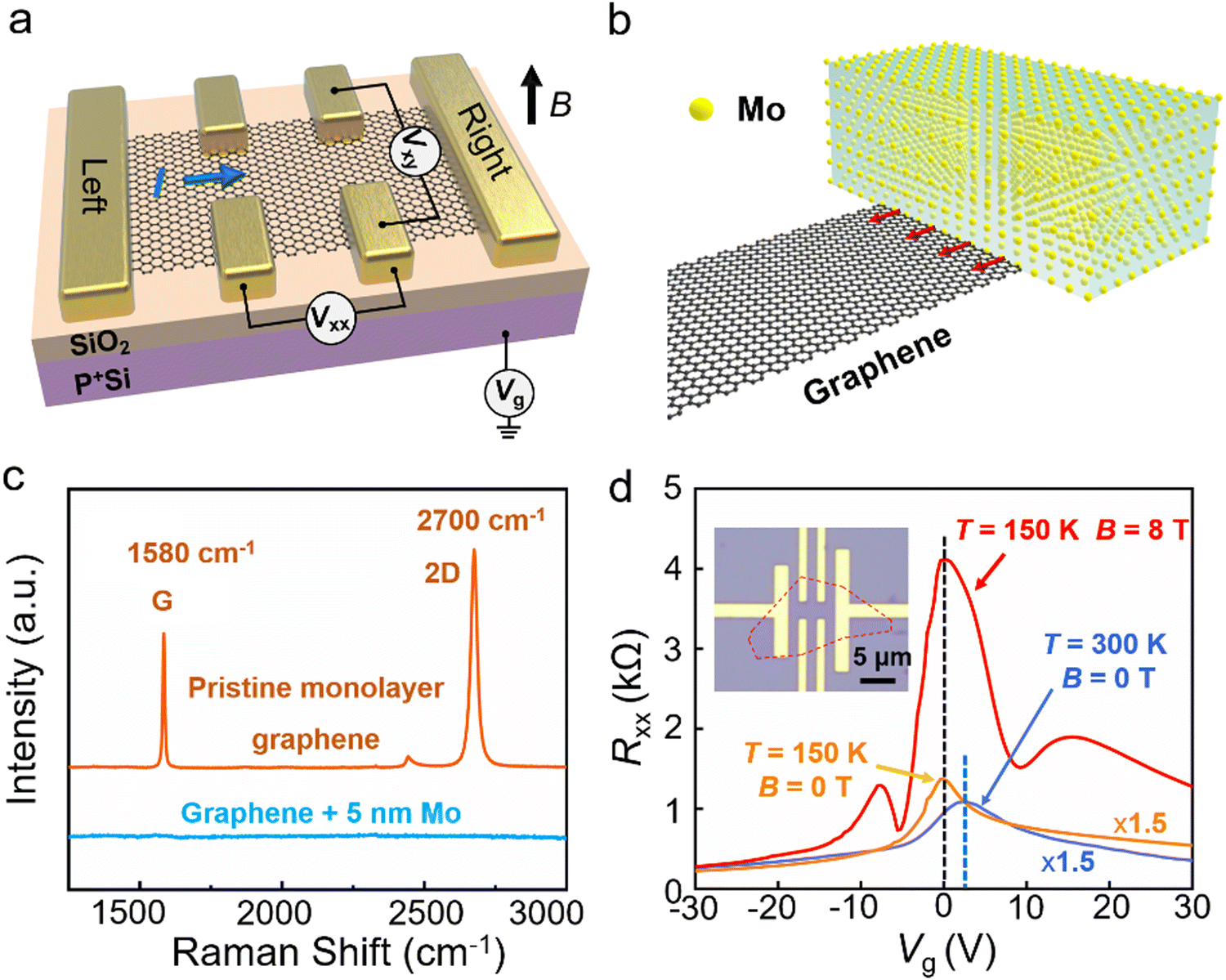 | ||
| Fig. 1 Structure and gate modulation of the longitudinal resistance Rxx of an edge-bonded Hall bar device using pristine monolayer graphene. (a) A schematic showing the structure and measurement scheme of the graphene device with the Hall-bar-type electrode configuration. The driving current, gate voltage, longitudinal voltage, Hall voltage and external magnetic field are represented as I, Vg, Vxx, Vxy and B, respectively. (b) Schematic view of the right electrode of the Hall bar configuration in (a). An edge-bonded contact is formed through a local solid–solid reaction between carbon atoms of graphene and Mo atoms. The red arrows here indicate magnetic moments and long-range ferromagnetic order revealed by the anomalous Hall effect. (c) Comparison of the Raman spectra of pristine monolayer graphene with that after covering 5 nm Mo. The characteristic G and 2D peaks for pristine monolayer graphene disappear after the deposition of Mo. This indicates that a solid–solid reaction occurs between graphene and Mo atoms; thus, an edge-bonded Hall-bar-type configuration can be fabricated in one step. (d) Typical Rxxversus the gate voltage Vg in a monolayer graphene Hall device with edge-bonded contacts. The blue curve corresponds to Rxx measured at room temperature under atmospheric conditions at a zero magnetic field (for comparison, the curve is multiplied with a factor of 1.5). From the peak position of Rxx, VDirac is found to be around ∼2.4 V. The yellow curve corresponds to this after the device is loaded into PPMS and the temperature is 150 K. VDirac is shifted to close to zero voltage and the peak value of Rxx increases to ∼898 Ω. After a perpendicular magnetic field of 8.0 T is applied, VDirac remains at a zero voltage but the peak value increases to ∼4.1 kΩ (red curve). Rxx exhibits pronounced oscillatory features under a magnetic field of 8.0 T. The optical micrograph of the graphene Hall device is shown in the inset. | ||
Fig. 1d shows the gate modulation of the longitudinal resistance Rxx at temperatures of 150 and 300 K and magnetic fields of 0 and 8 T in a typical monolayer graphene device with edge-bonded contacts, respectively. Here, the blue curve corresponds to Rxx as a function of Vg measured at room temperature under atmospheric conditions at a zero magnetic field. From the peak position of Rxx, VDirac is found to be around 2.4 V. The peak of Rxx has a value of ∼725 Ω, which may vary from 350 to 1200 Ω in the 12 devices that we have measured. And the mobility can be obtained from the Hall data, which is in the range of 4000–12![[thin space (1/6-em)]](https://www.rsc.org/images/entities/char_2009.gif) 000 cm2 V−1 S−1. After loading into PPMS and vacuum pumping, Rxx as a function of Vg is obtained as shown by the yellow curve in Fig. 1d at a temperature of 150 K. It can be seen that VDirac is shifted to close to zero and the peak value of Rxx increases to ∼ 898 Ω. When a perpendicular magnetic field of 8 T is applied, VDirac remains at zero voltage but the peak value of Rxx increases to ∼4.1 kΩ (red curve). This indicates a positive, giant magnetoresistance (MR) of 358%; here, MR is defined as [R(B) − R(0)]/R(0), where R(B) and R(0) are the resistances at an applied field and a zero field, respectively. Under a magnetic field of 8 T, the longitudinal resistance Rxx exhibits pronounced oscillatory features.
000 cm2 V−1 S−1. After loading into PPMS and vacuum pumping, Rxx as a function of Vg is obtained as shown by the yellow curve in Fig. 1d at a temperature of 150 K. It can be seen that VDirac is shifted to close to zero and the peak value of Rxx increases to ∼ 898 Ω. When a perpendicular magnetic field of 8 T is applied, VDirac remains at zero voltage but the peak value of Rxx increases to ∼4.1 kΩ (red curve). This indicates a positive, giant magnetoresistance (MR) of 358%; here, MR is defined as [R(B) − R(0)]/R(0), where R(B) and R(0) are the resistances at an applied field and a zero field, respectively. Under a magnetic field of 8 T, the longitudinal resistance Rxx exhibits pronounced oscillatory features.
Fig. 2a and c display the color map and curves of Rxx as a function of the gate voltage Vg and the applied magnetic field B at a temperature of 150 K, respectively. This device is the same one as that shown in Fig. 1d (device 1). The applied magnetic field B is perpendicular to the graphene with a strength from −8.0 to 8.0 T with a step of 0.5 T. The following two features can be observed: first, as shown in Fig. 2c, the peak position of Rxx, i.e., the charge-neutral Dirac point, VDirac, is around zero and does not change with the applied magnetic fields in the range of 0.5–8.0 T. At VDirac, an unexpected, giant and positive MR of Rxx is observed in Fig. S2 (ESI†).18 This suggests a potential quantum-mechanical origin due to the charge neutral nature at the Dirac point. Second, under high magnetic fields, Rxxversus Vg exhibits pronounced oscillatory features. At a magnetic field of 8.0 T, typical values of the peaks and valleys of Vg are shown in Fig. 2c, which are −20.4, −13.6, −12.0, −8.4 and −5.6 V, respectively. The dependence of these Vg on the magnetic field is linear as shown in Fig. S3 (ESI†).18 The two lines of L−20.4 and L−13.6 ∝ B intersect at a magnetic field of ∼2.5 T, here L−20.4 representing the straight line starting at Vg = −20.4 V, etc. (Fig. S3, ESI†). And the two lines of L−12.0 and L−8.4 intersect at a magnetic field of ∼3.5 T. These observations suggest a mechanism induced by high magnetic fields and we attribute the mechanism to be originated from Zeeman splitting of Landau Levels and discuss them in more detail below with Fig. 2d.
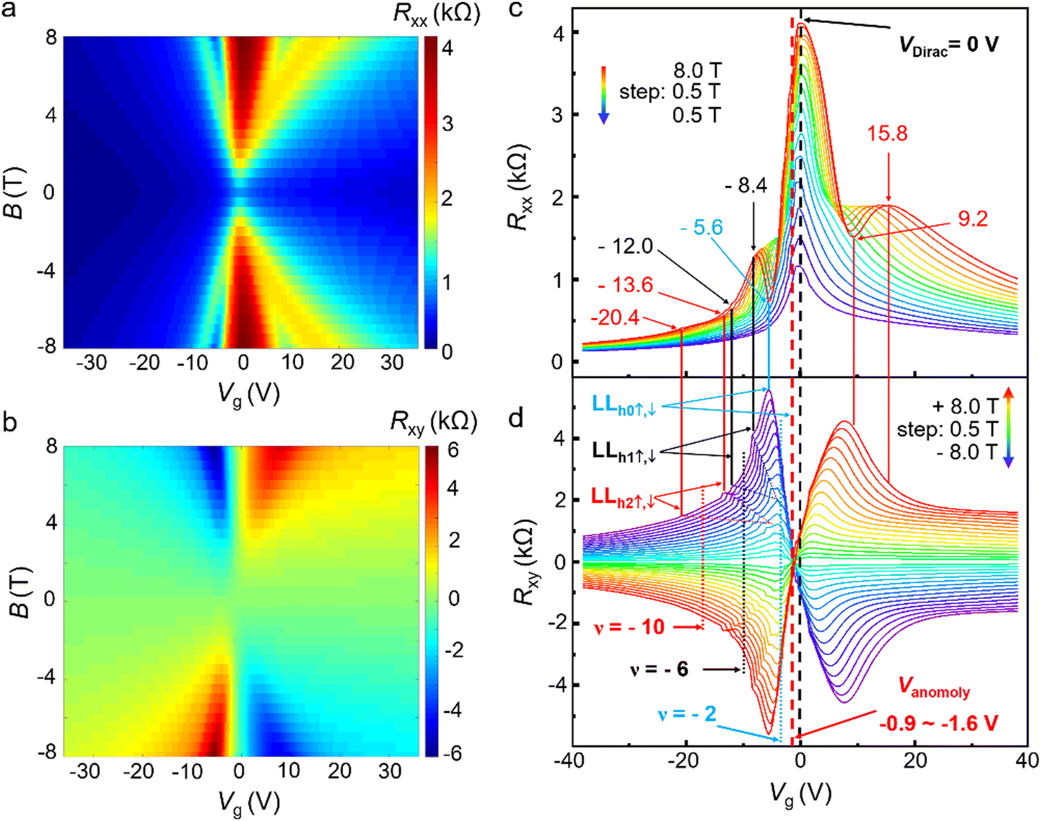 | ||
| Fig. 2 Color maps of the longitudinal resistance Rxx, Hall resistance Rxy and their dependence on the gate voltage Vg and the magnetic field B at a temperature of 150 K (device 1). (a) Color map of Rxx as a function of the back gate voltage Vg and the external magnetic field B. Data are taken from −38 to 38 V for Vg and −8.0 to 8.0 T for B (symmetrized). (b) Color map showing Rxy as a function of Vg and the external magnetic field B (anti-symmetrized). (c) 16 extracted curves of Rxxversus Vg under an external magnetic field B from 0.5 to 8.0 T with a step of 0.5 T. The sharp peak position of Rxx (VDirac) is around zero and does not change with the applied magnetic fields. At VDirac, an unexpected, giant and positive magnetoresistance (MR) is observed with a maximum value of ∼358%. Under high magnetic fields, Rxxversus Vg exhibits pronounced oscillatory features. Typical values of Vg are shown for a magnetic field of 8.0 T. (d) 32 extracted curves of Rxyversus Vg under an external magnetic field B from −8.0 to 8.0 T with a step of 0.5 T. At the characteristic peaks and valleys of Rxx (Vg), Rxy (Vg) exhibits plateaus at the corresponding gate voltages Vg. This feature is shown by the vertical lines between (c) and (d). When the magnetic field becomes smaller, the two red vertical lines move right and coincide. A similar feature is observed for the two black vertical lines. Another important observation here is that there is an anomalous gate voltage Vanomaly, at which Rxy becomes zero. The index of Landau-level (LL), their Zeeman splitting and the corresponding filling factors (ν = −2, −6, and −10) are shown. | ||
Fig. 2b and d display the color map and the curves of the Hall resistance Rxy as a function of the gate voltage Vg and the applied magnetic field B. An interesting feature that can be seen from Fig. 2c and d is that at the peaks and valleys of Rxx (Vg), Rxy (Vg) exhibits plateaus at the corresponding gate voltages. This feature is shown by the vertical lines between Fig. 2c and d. The two vertical red lines represent the values of Vg at −20.4 and −13.6 V for a magnetic field of 8.0 T. When the magnetic field decreases, these two lines move towards right, i.e., the corresponding absolute values of Vg become smaller. This feature can be seen clearly with the two straight dotted lines in Fig. 2d, suggesting a linear relationship between Vg and the magnetic field B. Similar characteristics can be observed between the two black vertical lines, which represent Vg at −12.0 and −8.4 V for a magnetic field of 8.0 T. These results suggest that the two red and black vertical lines have the same origin and we attribute it to be caused by the Landau level (LL) formation and Zeeman splitting of these LLs under a perpendicular magnetic field B. As a matter of fact, the filling factors have been calculated, which correspond to −10 and −6 for the two red and black vertical lines, respectively (Fig. S4, ESI†). Meanwhile, the Landau level index n = 0 with a filling factor of 2 has also been resolved as shown in Fig. 2d.
Another interesting observation from Fig. 2d is that there is an anomalous gate voltage Vanomaly, at which the Hall resistivity Rxy becomes zero. An oscillatory structure of Vanomaly as a function of the magnetic field can be seen from Fig. S4 (ESI†): the smallest (−1.58 V) and largest (−0.90 V) of Vanomaly correspond to a magnetic field of 0.5 T and a range of magnetic field of 5.5–7.0 T, respectively. This means that Vanomaly is in a very narrow range of 0.68 V. The origin and mechanism of this Vanomaly are attributed to the ferromagnetism in pristine monolayer graphene and will be explained in detail below.
To further reveal the existence of the AHE and ferromagnetism in pristine monolayer graphene, we extract more data from Fig. 2a and b and display them in Fig. 3. Fig. 3a shows the Hall resistance Rxy as a function of the external magnetic field B for VDirac = 0 V (charge-neutral point), Vg = +25 V (electron carrier) and Vg = −25 V (hole carrier) with dotted curves, respectively. It can be seen that all three curves of Rxy exhibit nonlinear behaviors. In general, the observed nonlinearity in Rxy suggests the following two possible scenarios: (1) the ordinary Hall effect arising from more than one type of carriers in response to the external magnetic field and (2) the AHE from spin-polarized carriers which are attributed to the presence of the FM order.10 For the first case, we deliberately avoid the region close to the Dirac point where both electrons and holes coexist, and the observed AHE sign still remains at Vg = ±25 V, which rules out this cause. Therefore, in our work, we attributed the nonlinearity in Rxy to the presence of the FM order in graphene.2,3,10 Considering that Mo is paramagnetic and graphene is diamagnetic in the bulk, there are two potential sources for graphene magnetism. One is the impurity in graphene. The graphene in this work is derived from the mechanical stripping of natural graphite, thus excluding the influence of impurity. The second possibility is the edge magnetism of graphene,20,21 and the experiment work22 clearly demonstrates the spin ordering along the edge of graphene. Considering that the all-dangling bonds of graphene are passivated by bonds to Mo atoms, the long-range ferromagnetic order and ferromagnetism in this work are attributed to be located at the edges between Mo contacts and monolayer graphene.22
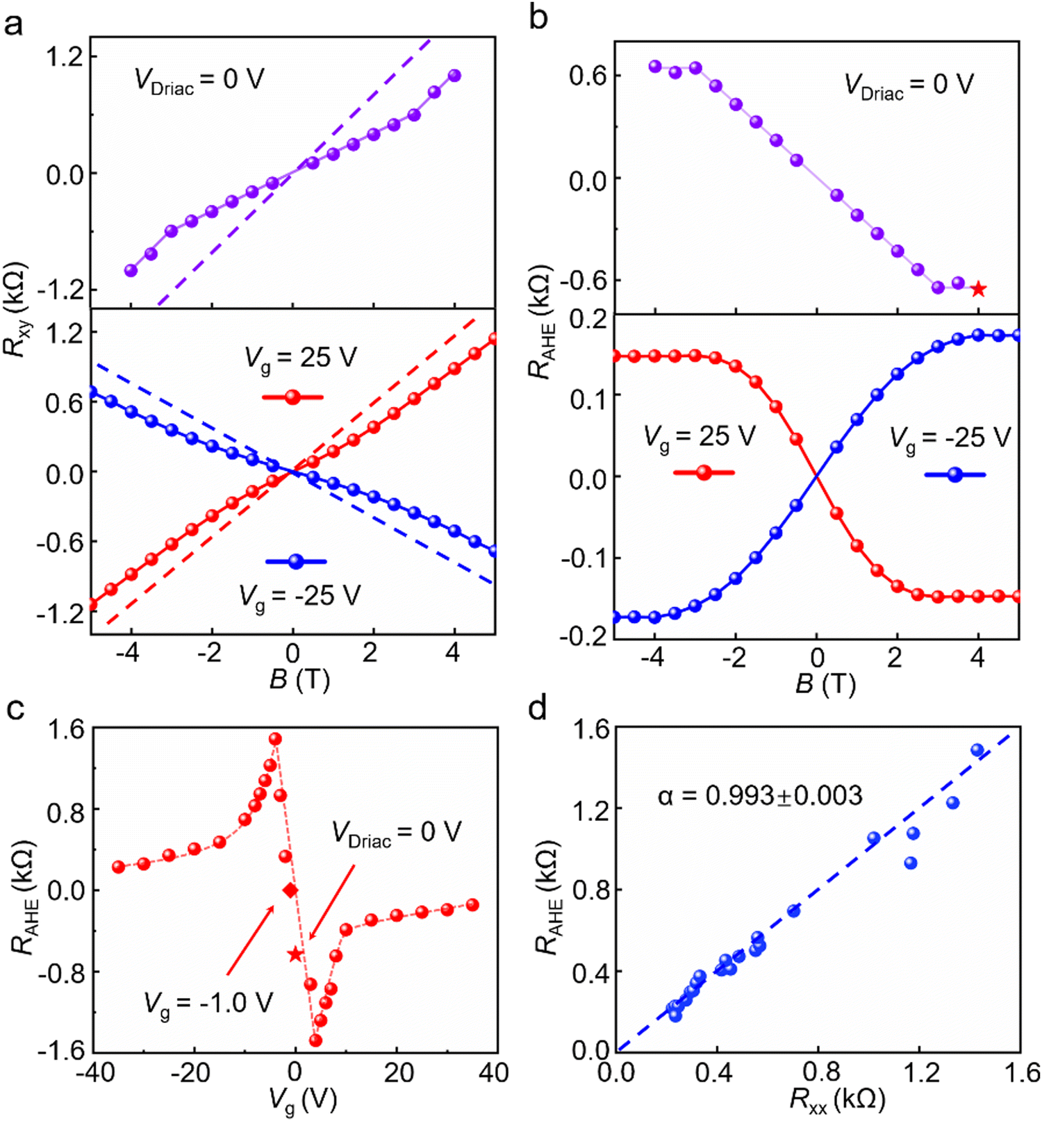 | ||
| Fig. 3 Characteristics of the Hall resistance Rxy and anomalous Hall resistance RAHE extracted from Fig. 2. (a) Rxy as a function of the external magnetic field B at VDirac (0 V) and Vg = ±25 V. The Hall resistance Rxy (dotted line) exhibits nonlinearity and consists of two contributions: R (B) + RAHE (M). Here, R (B) comes from the ordinary Hall effect, which is extrapolated from high-field data and shown as the dashed line. It is worth noting that both slopes are positive for the Rxy ∝ B curves of electron carriers (Vg = 25 V) and of the charge neutral point VDirac; meanwhile the slope for hole carriers (Vg = −25 V) is negative. (b) Anomalous Hall resistance RAHE obtained by subtracting the linear background in (a). An “X” pattern is observed between the two RAHE curves for electron and hole carriers. The RAHE ∝ B curve at VDirac displays similar trends to that for electron carriers. A unique feature of RAHE at VDirac is observed: perfect linear dependence on the magnetic field until the RAHE reaches a saturated value of ∼653 Ω. (c) The saturated RAHE as a function of Vg. The variation of the saturated RAHE with Vg is similar to that of Rxy as shown in Fig. 2(d). RAHE becomes zero at Vg = −1.0 V. It is interesting to note that at VDirac, RAHE has a negative value of -653 Ω as shown by the red star. (d) The saturated RAHEversus Rxx. The blue dots represent the saturated RAHE for the hole polarity and the blue dashed straight line indicates the fit with a power RAHE ∝ Rαxx with α = 0.993 ± 0.003. This indicates a linear relationship between the saturated RAHE and Rxx, suggesting an extrinsic mechanism, i.e., the skew scattering mechanism of the observed AHE. | ||
As in usual ferromagnets,2,10 the nonlinearity of Rxy can be described as a sum of two terms: Rxy = R(B) + RAHE(M) = αB + βM, where B is the external magnetic field, M is the magnetization component in the perpendicular direction, α = ±1/en (“+”, electron carrier and “−”, hole carrier), β is the M-independent parameter and n is the concentration of carrier, respectively. The B-linear term results from the Lorentz force on the electron (hole) carrier as in the ordinary Hall effect. This contribution is shown in Fig. 3a as straight dashed lines. The purple and red straight dashed lines in Fig. 3a correspond to those at VDirac (neutral charge point) and at Vg = +25 V (electron carrier), respectively. The blue straight dashed line corresponds to that at Vg = −25 V (hole carrier). The slope of Rxyversus B for electron carriers (Vg = +25 V) is positive, i.e., Rxy increases with the increase of the magnetic field B. In contrast, the slope for hole carriers (Vg = −25 V) is negative, i.e., Rxy decreases with the increase of the magnetic field B. This results in a “×” pattern as shown in the lower part of Fig. 3a. It is interesting to note that the slope for the charge neutral Dirac point is also positive as shown in the upper part of Fig. 3a. This observation is quite novel and interesting compared to those in the conventional Hall effect.7–9 Because this means that if the carrier concentration tends to become zero, Rxy also exists and behaves as an electron-like carrier. One possible reason is that both VDirac and Vg for the electron carrier (Vg > 0) are at the right side of Vanomaly and the exact mechanism remains to be understood.
The anomalous Hall resistance RAHE can be obtained by subtracting the linear background in Fig. 3a. As shown by the blue dotted curve in the lower part of Fig. 3b, for the hole carrier (Vg = −25 V), RAHE increases linearly with the increase of the magnetic field in the field range of −2 to 2 T. When the magnetic field is further increased, RAHE saturates gradually to a value of 173 Ω. The red dotted curve in the lower part of Fig. 3b displays RAHEversus B for electron carriers (Vg = +25 V). Here, RAHE decreases when the magnetic field increases in the range of −1.5 to 1.5 T with a linear relationship. And RAHE becomes saturated with a value of −147 Ω when the magnetic field is further increased. Thus, an “X” pattern is observed between the two RAHE curves for electron and hole carriers. The purple dotted curve in the upper part of Fig. 3b displays RAHE at VDirac = 0 V. The change curve of Rxy with different magnetic field intensities B at VDirac displays similar trends to that for electron carriers. Meanwhile, unique features of RAHE at VDirac are observed, such as perfect linear dependence on the magnetic field until RAHE reaches the saturated value, which has an absolute value of 653 Ω.
Fig. 3c shows the saturated values of RAHE as a function of the gate voltage Vg. It can be seen that the variation of the saturated RAHE is similar to that for Rxy as shown in Fig. 2d. And the saturated RAHE becomes zero at Vg = −1.0 V, which is in the range of −0.9 to −1.6 V of Vanomaly. It is interesting to note that at VDirac, RAHE has a negative value of −653 Ω as shown by the blue star in Fig. 3c. In order to have a better understanding of the inducing mechanism of the AHE, the saturated RAHE as a function of Rxx is extracted from Fig. 2 and is shown in Fig. 3d. The blue dots represent the saturated RAHE for hole polarity and the blue dashed straight line indicates the fit with a power law RAHE ∝ Rxxα with α = 0.993 ± 0.003. This indicates a linear relationship between the saturated RAHE and Rxx, suggesting an extrinsic mechanism, i.e., the skew scattering mechanism of the observed AHE.2
Therefore, the mechanism for the observation of Vanomaly in Fig. 2 can be explained as follows: the Hall resistance Rxy consists of two terms2,10–12 as discussed above, i.e., Rxy = αB + βM. Since Vanomaly has a negative value, this induces hole carriers in the Hall device and results in a negative value of α. We assume MG = χGB (χG: magnetic susceptibility of graphene), where MG is the magnetization of graphene. Thus, we have Rxy = αB + βMG = (−|α| + βχG) B = 0, which results in a zero Rxy and does not depend on the strength of the magnetic field.
Fig. 4 displays the temperature-dependent characteristics of Rxy, Rxx and RAHE for another Hall device based on a pristine monolayer graphene (device 2). The longitudinal resistance Rxx as a function of the magnetic field is measured in the temperature range of 2–300 K (Fig. 4a). At a temperature of 300 K, as shown in the inset of Fig. 4a, Rxx increases from 1219 Ω (zero magnetic field) to 3381 Ω (6.0 T). This gives a giant positive MR of ∼177%, which is more than an order of magnitude larger than that observed in the magnetite nanowire.23 When the temperature decreases (100, 150 and 200 K), obvious nonlinear behaviors of Rxx curves appear. And at temperatures of 50, 20 and 2 K, the curves of Rxx exhibit oscillatory structures.
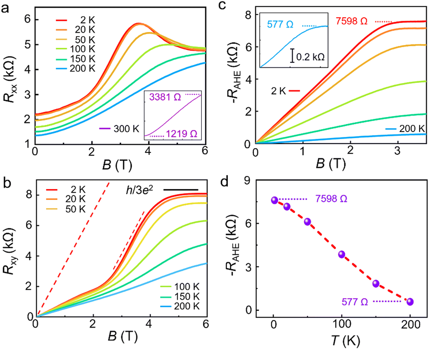 | ||
| Fig. 4 Temperature-dependent characteristics of Rxx, Rxy and RAHE of another pristine monolayer graphene (device 2). (a) The longitudinal resistances Rxx as a function of the magnetic field B measured in the temperature range of 2–300 K. At a temperature of 300 K, Rxx increases from 1219 Ω (zero magnetic field) to 3381 Ω (6.0 T) as shown in the inset, resulting a giant positive MR of ∼177%. As the temperature decreases, the curves of Rxx exhibit oscillatory structures. (b) Six curves of Rxyversus the magnetic field B at different temperatures. It can be seen that all the 6 curves of Rxy exhibit nonlinear behaviors in the field range of 0–4 T. The plateau value of Rxy reaches ∼0.94h/3e2 at a temperature of 2 K, while Rxx decreases but does not yet reach zero. These observations are early indications of the QAH effect with a filling factor of 3. The straight red dotted line represents the ordinary Hall background at a temperature of 2 K. (c) Six curves of RAHEversus the magnetic field B at different temperatures after the linear Hall background are removed from the data in (b). At a temperature of 2 K, the RAHE increases linearly with the magnetic field in the range of 0–2.5 T. Then RAHE gradually saturates at 3–3.5 T and reaches a saturation value of 7598 Ω (∼ 0.88h/3e2). When the temperature increases, it takes a higher magnetic field for RAHE to reach saturation. At a temperature of 200 K, RAHE saturates at a field of ∼ 4.0 T with a value ∼577 Ω as shown in the inset. (d) The saturation value of RAHEversus temperature at 2, 20, 50, 100, 150 and 200 K. When the temperature increases, the RAHE decreases accordingly. | ||
The curves of the Hall resistance Rxy as a function of the magnetic field B are shown in Fig. 4b and Fig. S6 (ESI†) in the temperature range of 2–300 K. It can be seen from Fig. 4b that all the 6 curves of Rxy exhibit nonlinear behaviors in the field range of 0–4 T, which are similar to those in Fig. 3 for device 1. The two curves for temperatures of 2 and 20 K have a little difference at a low magnetic field of 0–3 T; and when the magnetic field increases to 4–6 T, Rxy gradually saturates and plateaus are well-developed. The plateau value of Rxy reaches ∼0.94h/3e2 at a temperature of 2 K, while Rxx decreases but does not yet reach zero. These observations are early indications of the QAH effect with a filling factor of 3, which is distinctively different from those reported previously.8,9 It is important to note that for device 1, when the temperature is less than 2 K, pronounced plateau-like features are observed in Rxy while Rxx exhibits pronounced SdH oscillations (Fig. S7, ESI†).
The red straight dotted lines in Fig. 4b represent the ordinary Hall background as discussed previously in Fig. 3. After these linear ordinary Hall backgrounds are subtracted, the anomalous Hall resistance RAHE is obtained and shown in Fig. 4c. It can be seen that at a temperature of 2 K, the RAHE increases linearly with a magnetic field in the range of 0–2.5 T. Then RAHE gradually saturates at 3–3.5 T and reaches a saturation value of 7598 Ω, which is ∼0.88h/3e2. When the temperature increases, the saturation value of RAHE decreases in the temperature range of 2–200 K as shown Fig. 4d. Meanwhile, the magnetic field becomes larger for RAHE to reach the saturation value. For example, at a temperature of 200 K, RAHE saturates at a field of ∼4.0 T with a value ∼577 Ω as shown in the left inset of Fig. 4c. No obvious saturation behavior is observed at a temperature of 250 K and a high magnetic field of ∼5.0 T is needed for RAHE to reach saturation at a temperature of 300 K (Fig. S6, ESI†).
It is important to note that the Hall resistance Rxy of the AHE can be used to probe the magnetic anisotropy of thin ferromagnetic films.3,5,10 If the curve of Rxyversus B develops a hysteresis loop, it indicates a long-range ferromagnetic order and ferromagnetism with out-of-plane magnetic anisotropy.3,5 Meanwhile, if the curve of Rxy shows nonlinear dependence on the magnetic field B but no hysteresis loop appears, it indicates ferromagnetism and in-plane magnetic anisotropy.10 In this work, both Rxx and Rxy as a function of the magnetic field have been measured with a sweeping rate of 0.001 T/second. No hysteresis loops have been observed (Fig. S8, ESI†), indicating in-plane magnetic anisotropy of the ferromagnetism at the edges between the Mo contacts and the monolayer graphene as shown schematically in Fig. 1b.
3. Conclusions
In summary, by using an edge-bonded Hall bar, we have provided indisputable evidence of the existence of the AHE in pristine monolayer graphene. The longitudinal resistance Rxx shows a positive and giant MR and pronounced Shubnikov-de Haas oscillations while Rxy exhibits plateau-like features. Plateaus of Rxy ∼ 0.94h/3e2 and RAHE ∼ 0.88h/3e2 have been observed while the longitudinal resistance Rxx decreases, suggesting the existence of the QAH in pristine graphenes. The ferromagnetism in pristine monolayer graphene can still be observed at a temperature as high as 300 K, which raises exciting questions on ferromagnetism in lower dimensions24,25 and may lead to new applications in pure carbon-based devices26,27 and spintronics.23,284. Experimental section
Device fabrication
The graphene hall bar devices were fabricated from high-quality monolayer graphene using a mechanical stripping meathod.8,9,29,30 Firstly, graphene flakes were exfoliated from natural graphite (Alfa Aesar) by using Scotch transparent tape (3 M) and then were transferred onto p-type doped Si substrates (10 × 10 mm2) with 285 nm SiO2. Monolayer graphene flakes were identified by optical contrast under an optical microscope (Leica DM4000), and their positions were recorded under ×100 magnification. The layer number of graphene was further identified with a combination of Raman spectroscopy (Fig. S9, ESI†)18 and atomic-force microscopy (Fig. S10 and S11, ESI†).18 Based on the position and orientation of graphene, the graphene flakes were then patterned using poly(methyl methacrylate) (PMMA, ∼600 nm thick) and electron-beam lithography (Vistec EBPG 5000plus ES) followed by developing with 1:3 MIBK: IPA solution. After this, 50–80 nm Mo was deposited with magnetron sputtering (Lesker Lab 18) at a pressure of 10−5 torr and a power of 150 W followed by lift-off in acetone at 70 °C. The atomic force microscopy (AFM) topographic image was obtained by AFM (Bruker, Multimode 8-HR) in a tapping mode. Raman measurements were carried out using micro-Raman spectroscopy (Renishaw in Via Raman Spectroscope) under ambient conditions with a laser wavelength of 514 nm. The laser power was kept below 0.5 mW, and a 100× objective lens with a numerical aperture of 0.90 can offer a laser spot size of ∼1 μm. Several spectra were collected to ensure the credibility and repeatability of the results.
Device measurement
For the characterization of devices at room temperature under atmospheric conditions, electrical characterization studies of the graphene hall bar device were performed using an Agilent B1500A Semiconductor Device Analyzer and a probe station. The magnetotransport measurements were performed using a physical property measurement system (PPMS) equipped with a magnetic field in the range of 0–9 T and the temperature in the range of 2–300 K. Transport properties were measured in standard Hall bar geometry through the standard lock-in technique with an AC current of 5 μA (13 Hz). We changed the current to ensure the credibility and repeatability of the transport results, and found no signal variation upon changing the current amplitude.Author contributions
L. F. S., W. G. C. and Y. J. L. supervised the project. H. L. and Z. S. P. conceived and designed the device structure. H. W., H. L., and Z. S. P. designed and built the experimental setup with the help of J. Y. J. and Z. P. W. H. L., K. P. and W. G. C. fabricated and characterized the graphene devices. H. L., Z. S. P. and H. W. performed the measurements. H. L., H. W., Z. S. P., L. F. S., D. Z. and Y. J. L. analyzed the data with support from W. X. W., Y. S. X., Y. W. and Z. W. L. F. S., H. L., Z. S. P., W. G. C. and H. W. co-wrote the manuscript with contributions from all other authors. All the authors discussed the results and commented on the manuscript.Conflicts of interest
There are no conflicts to declare.Acknowledgements
This work was supported by the Major Nanoprojects of Ministry of Science and Technology of China (Grant No. 2018YFA0208403), the CAS Project for Young Scientists in Basic Research (YSBR-030), the GBA National Institute for Nanotechnology Innovation, Guangdong, China (2020B0101020003), the National Natural Science Foundation of China (21973021) and the Strategic Priority Research Program of Chinese Academy of Sciences (Grant No. XDB36000000).References
- E. H. Hall, Philos. Mag., 1880, 10, 301–328 Search PubMed.
- N. Nagaosa, J. Sinova, S. Onoda, A. H. MacDonald and N. P. Ong, Rev. Mod. Phys., 2010, 82, 1539–1592 CrossRef.
- B. J. Tang, X. W. Wang, M. J. Han, X. D. Xu, Z. W. Zhang, C. Zhu, X. Cao, Y. M. Yang, Q. D. Fu, J. Q. Yang, X. J. Li, W. B. Gao, J. D. Zhou, J. H. Lin and Z. Liu, Nat. Electron., 2022, 5, 224–232 CrossRef CAS.
- R. Yu, W. Zhang, H. J. Zhang, S. C. Zhang, X. Dai and Z. Fang, Science, 2010, 329, 61–64 CrossRef CAS PubMed.
- C. Z. Chang, J. Zhang, X. Feng, J. Shen, Z. Zhang, M. Guo, K. Li, Y. Ou, P. Wei, L. L. Wang, Z. Q. Ji, Y. Feng, S. Ji, X. Chen, J. Jia, X. Dai, Z. Fang, S. C. Zhang, K. He, Y. Wang, L. Lu, X. C. Ma and Q. K. Xue, Science, 2013, 340, 167–170 CrossRef CAS PubMed.
- K. S. Novoselov, A. K. Geim, S. V. Morozov, D. Jiang, Y. Zhang, S. V. Dubonos, I. V. Grigorieva and A. A. Firsov, Science, 2004, 306, 666–669 CrossRef CAS PubMed.
- B. Y. Chen, L. Huang, X. M. Ma, L. J. Dong, Z. Y. Zhang and L. M. Peng, Carbon, 2015, 94, 585–589 CrossRef CAS.
- K. S. Novoselov, A. K. Geim, S. V. Morozov, D. Jiang, M. I. Katsnelson, I. V. Grigorieva, S. V. Dubonos and A. A. Firsov, Nature, 2005, 438, 197–200 CrossRef CAS PubMed.
- Y. B. Zhang, Y. W. Tan, H. L. Stormer and P. Kim, Nature, 2005, 438, 201–204 CrossRef CAS PubMed.
- Z. Y. Wang, C. Tang, R. Sachs, Y. Barlas and J. Shi, Phys. Rev. Lett., 2015, 114, 016603 CrossRef CAS PubMed.
- C. L. Tang, Z. W. Zhang, S. Lai, Q. H. Tan and W. B. Gao, Adv. Mater., 2020, 32, 1908498 CrossRef CAS PubMed.
- H. D. Song, P. F. Zhu, J. Z. Fang, Z. Q. Zhou, H. Yang, K. Y. Wang, J. B. Li, D. P. Yu, Z. M. Wei and Z. M. Liao, Phys. Rev. B, 2021, 103, 125304 CrossRef CAS.
- F. D. M. Haldane, Phys. Rev. Lett., 1988, 61, 2015–2018 CrossRef CAS PubMed.
- Z. H. Qiao, S. Y. A. Yang, W. X. Feng, W. K. Tse, J. Ding, Y. G. Yao, J. Wang and Q. Niu, Phys. Rev. B: Condens. Matter Mater. Phys., 2010, 82, 161414 CrossRef.
- Z. H. Qiao, W. Ren, H. Chen, L. Bellaiche, Z. Y. Zhang, A. H. MacDonald and Q. Niu, Phys. Rev. Lett., 2014, 112, 116404 CrossRef PubMed.
- J. Liu, Z. S. Peng, J. Z. Cai, J. Y. Yue, H. N. Wei, J. Impundu, H. Liu, J. Y. Jin, Z. Yang, W. G. Chu, Y. J. Li, G. T. Wang and L. F. Sun, Nano Today, 2021, 38, 101138 CrossRef CAS.
- W. Han, R. K. Kawakami, M. Gmitra and J. Fabian, Nat. Nanotechnol., 2014, 9, 794–807 CrossRef CAS PubMed.
- ESI.†.
- Q. Cao, S.-J. Han, J. Tersoff, A. D. Franklin, Y. Zhu and Z. Zhang, Science, 2015, 350, 68–72 CrossRef CAS PubMed.
- M. Fujita, K. Wakabayashi, K. Nakada and K. Kusakabe, J. Phys. Soc. Jpn., 1996, 65, 1920–1923 CrossRef CAS.
- R. E. Blackwell, F. Zhao, E. Brooks, J. Zhu, I. Piskun, S. Wang, A. Delgado, Y.-L. Lee, S. G. Louie and F. R. Fischer, Nature, 2021, 600, 647–652 CrossRef CAS PubMed.
- H. Q. Zhou, H. C. Yang, C. Y. Qiu, Z. Liu, F. Yu, M. J. Chen, L. J. Hu, X. X. Xia, H. F. Yang, C. Z. Gu and L. F. Sun, J. Phys. Chem. C, 2011, 115, 15785–15792 CrossRef CAS.
- Z. M. Liao, Y. D. Li, J. Xu, J. M. Zhang, K. Xia and D. P. Yu, Nano Lett., 2006, 6, 1087–1091 CrossRef CAS PubMed.
- N. D. Mermin and H. Wagner, Phys. Rev. Lett., 1966, 17, 1133–1136 CrossRef CAS.
- P. Gambardella, A. Dallmeyer, K. Maiti, M. C. Malagoli, W. Eberhardt, K. Kern and C. Carbone, Nature, 2002, 416, 301–304 CrossRef CAS PubMed.
- Z. F. Wan, X. Chen and M. Gu, Opto-Electron. Adv., 2021, 4, 200079 CAS.
- S. Q. Yan, Y. Zuo, S. S. Xiao, L. K. Oxenløwe and Y. H. Ding, Opto-Electron. Adv., 2022, 5, 210159 CAS.
- Z. Liu, L. Li, L. Cui, Y. Shi, T. Song, J. Cai, X. Cui, X. Jiang and J. Zhao, Nanoscale Horiz., 2021, 6, 283 RSC.
- Y. B. Zhang, J. P. Small, E. S. Amori and P. Kim, Phys. Rev. Lett., 2005, 94, 176803 CrossRef PubMed.
- H. Q. Zhou, C. Y. Qiu, Z. Liu, H. C. Yang, L. J. Hu, J. Liu, H. F. Yang, C. Z. Gu and L. F. Sun, J. Am. Chem. Soc., 2010, 132, 944–946 CrossRef CAS PubMed.
Footnotes |
| † Electronic supplementary information (ESI) available. See DOI: https://doi.org/10.1039/d3nh00233k |
| ‡ These authors contributed equally to this work. |
| This journal is © The Royal Society of Chemistry 2023 |