
Emerging memristive artificial neuron and synapse devices for the neuromorphic electronics era
Jiayi
Li
 a,
Haider
Abbas
a,
Diing Shenp
Ang
*a,
Asif
Ali
a and
Xin
Ju
b
a,
Haider
Abbas
a,
Diing Shenp
Ang
*a,
Asif
Ali
a and
Xin
Ju
b
aSchool of Electrical and Electronics Engineering, Nanyang Technological University, 50 Nanyang Avenue, Singapore 639798. E-mail: edsang@ntu.edu.sg
bInstitute of Materials Research and Engineering (IMRE), Agency for Science, Technology and Research (A*STAR), 2 Fusionopolis Way, Singapore 138634
First published on 7th August 2023
Abstract
Growth of data eases the way to access the world but requires increasing amounts of energy to store and process. Neuromorphic electronics has emerged in the last decade, inspired by biological neurons and synapses, with in-memory computing ability, extenuating the ‘von Neumann bottleneck’ between the memory and processor and offering a promising solution to reduce the efforts both in data storage and processing, thanks to their multi-bit non-volatility, biology-emulated characteristics, and silicon compatibility. This work reviews the recent advances in emerging memristive devices for artificial neuron and synapse applications, including memory and data-processing ability: the physics and characteristics are discussed first, i.e., valence changing, electrochemical metallization, phase changing, interfaced-controlling, charge-trapping, ferroelectric tunnelling, and spin-transfer torquing. Next, we propose a universal benchmark for the artificial synapse and neuron devices on spiking energy consumption, standby power consumption, and spike timing. Based on the benchmark, we address the challenges, suggest the guidelines for intra-device and inter-device design, and provide an outlook for the neuromorphic applications of resistive switching-based artificial neuron and synapse devices.
 Jiayi Li | Jiayi Li received his bachelor's degree in electronics from Tongji University, China. He is currently a PhD student at School of Electrical and Electronic Engineering, Nanyang Technological University, Singapore. His research interests are focused on micro/nano device fabrication for next-generation memories and neuromorphic and retinomorphic applications. |
 Haider Abbas | Dr Haider Abbas obtained his BS degree from Sir Syed University of Engineering and Technology, Pakistan in 2014 and PhD degree from Myongji University, South Korea in 2019. He worked at Hanyang University, South Korea as a Postdoctoral Researcher and a Research Assistant Professor from 2019 to 2022. In 2022, he joined Neuromorphic Device Lab at the School of Electrical and Electronic Engineering, Nanyang Technological University, Singapore as a Research Fellow. His research focusses on brain-inspired memristive devices for next-generation memory and neuromorphic computing applications. |
 Diing Shenp Ang | Prof. Diing Shenp Ang obtained his PhD degree in electrical engineering from the National University of Singapore. At present, he is a tenured faculty member in the School of Electrical and Electronic Engineering, Nanyang Technological University, Singapore. Earlier, he had conducted research on front end CMOS reliability. His current research interests are focused on the development of neuromorphic building blocks, resistive switching devices for storage class memory and radio frequency switch applications. |
 Asif Ali | Dr Asif Ali obtained his BS degree in electronics from Comsats University Islamabad, Pakistan. He obtained his MS degree in Electronic Engineering from Myongji University, South Korea in 2017 and his PhD degree in Nanotechnology and Advanced Materials Engineering from Sejong University, South Korea in 2021. He has joined School of Electrical and Electronic Engineering, Nanyang Technological University as a research fellow since then. His current research interests are focused on memristive devices and low dimensional semiconductor materials. |
 Xin Ju | Dr Xin Ju received his BEng degree in electronics science and technology from Tianjin University, Tianjin, China, in 2013, MS degree in microelectronics from Peking University, Beijing, China, in 2017, and PhD from Nanyang Technological University, Singapore in 2021. He is currently a Research Scientist in the 2D Semiconductor Materials and Devices group at the Institute of Materials Research and Engineering (IMRE). His research interests focus on next-generation nanoscale transistor and memory technologies, low dimensional semiconductor materials (e.g., 2D TMDCs), and characterization of the reliability and variability of novel electronic devices and their applications in artificial intelligence. |
1. Introduction
Ever since the conception of the McCulloch–Pitts neuron1 and perceptron2 models in the middle of the 20th century, artificial intelligence (AI) or artificial neural network (ANN) has largely remained a computer science terminology. Progress in the latter part of the century was hampered by the lack of computational power. Integrated circuit fabrication in the 1980–2000 period did not allow a high-density integration of transistors on a single processor and memory chip. Therefore, running simulations on a deep neural network (DNN) or a deep convolutional neural network (DCNN)3 and storing exponentially accumulated data were impractical in terms of time and energy costs even though ANN models were already relatively well established at that time.4–10 With increased chip density and the advent of multi-core processors such as the graphics processing unit (GPU) brought by the pursuit of Moore's law, coupled with more efficient ANN algorithms,3,11,12 the computational power bottleneck was successfully resolved at the beginning of this century. In 2012, a DNN with a billion connections was shown to be able to recognize highly conceptual objects such as a cat and the human body.13 In the same year, the DNN was shown to be on par with humans in terms of image classification accuracy (based on the MNIST database) and it even outperformed humans in traffic sign recognition.14 Introduced by Maass in 1995,15,16 spiking neural networks (SNNs) employ spiking neurons, also known as leaky integrate-and-fire (LIF) neurons, to compute. SNNs are regarded as the third generation ANN model classified by computational units, where the first generation is marked by the MCP model and the second is characterized with feedforward and recurrent sigmoidal neural nets, such as a rectified linear unit (ReLU), as well as networks of radial basis function units.17 The substantial difference between the second and third generation, as concluded by Roy et al.,18 lies in the dynamics of the signal: SNNs rely on the temporal dynamics (frequency and interval) of the binary incoming spikes, whereas the former uses the spatial dynamics (amplitude) of the signal.In recent years, researchers have focussed intently on implementing the SNN computing model on the current computational architecture (von Neumann architecture) and demonstrated excellent performance in visual and audio processing.19–29 In this regard, it is worth carrying out more comprehensive reviews on the emerging SNN software.18,30 However, like DNNs or CNNs, these are typically algorithms implementing different computational cores under conventional von Neumann architecture computing units, which limit the potential of the SNN for separating computation, transmission, and storage of the data. As in the brain, which the SNN dedicates to mimic, nerve cells and synapses not only transmit the signal electrically (spikes along axons) and chemically (neurotransmitters in synapses), but learn, compute, and memorize as well.
At this juncture, the AI community is confronted with another major challenge – the von Neumann bottleneck. This issue arises from the physically separated processor and memory units in the modern-day computer. While such an architecture could turnaround, in a relatively short time, a general computational job involving low data exchange between the processor and memory, it suffers from considerable time and energy overheads when executing computationally intensive ANN algorithms. The iterative and recursive nature of such algorithms results in a massive data exchange between the serially interfaced processor and memory, creating therefore a speed bottleneck. While outstanding algorithm optimization work by computer scientists31,32 has offered some respite, innovative hardware solutions are now deemed mandatory in view of the imminent data explosion in the current internet-of-things era.
The capability of the human brain in processing massive amounts of data in real time at a minute fraction of the energy cost of the most advanced computers has continued to amaze neuroscientists. In the pursuit of an efficient hardware platform for ANNs, the human brain therefore naturally serves as the golden guide. Attempts to extend existing digital circuit design methodologies to mimic the functionality of neurons and synapses in the biological neural network (CMOS-based SNN) have proven futile because of the large footprints and high energy cost of the resultant circuitries.33–35 Thus, the last few years have seen an intensive amount of research effort being directed toward developing alternative building blocks, commonly termed neuromorphic devices, that are both size and energy efficient, dedicated for implementing a neuromorphic-device-based SNN, the scope of which was reviewed by Marković et al. who discussed the underlying physics,36 Wang et al. who examined the material dependencies,37 and Zhang et al. who investigated the chip level implementation.38 Their works have envisioned a framework of the neuromorphic computing system, where neuromorphic devices will be the foundation.
Therefore, this review paper focuses on and summarizes recent major progress in building block neuromorphic devices. As similarly employed by Demise et al., terms “neuroscience” and “AI” are used to differentiate the biological/artificial intelligence,30 we carefully use “biological” for discussions on the study of the brain, biological neurons and synapses, and their relative behaviours and the term “neuromorphic” for discussions in the domain of electronic devices dedicated to emulate the function of the brain, and biomaterial is not within the scope of this work. This review is organized as follows: in Section II, we review the basic operation of the biological neural network. Since the exact function of the brain is still a subject of continuing research, only essential concepts that underpin current efforts towards a neuromorphic computer are emphasized. Section III details strategies that have been adopted in the current transition phase from von Neumann to a fully neuromorphic architecture. In Section IV, we compare various promising neuromorphic memristive candidates for artificial neurons and synapses. These devices are benchmarked according to their action energy and standby power consumption and spike timing. Section V concludes and presents challenges that remain to be tackled in this major shift in the computing paradigm, highlights potential guidelines for device design, and provides an outlook on the promising neural network level applications.
2. Biological neural network
This section describes the building blocks of a biological neural network and its fundamental roles and functions in the cognitive ability of living species. Although how exactly cognition develops is a major question to be answered, some basic principles have closely guided our current efforts in neuromorphic engineering.A. Basic functions of the biological neuron
Unlike in a von Neumann computer where a clear partition exists between the processor and memory, a biological neural network comprises a massive, distributed network of neurons,39 which serve as the basic “computational units”. A neuron receives input signals (data), in the form of voltage spikes or action potentials, from neighbouring neurons via synaptic junctions formed between axons of the transmitting (or pre-synaptic) neurons and dendrites of the receiving (or post-synaptic) neuron (Fig. 1a–c). A voltage spike arriving at the axon-end of a synapse triggers an ionic current, comprising sodium ions, that flows into the post-synaptic neuron. This in turn depolarizes the neuron, i.e., causes its membrane potential to increase positively from its negative rest level. As depicted in Fig. 1d, when enough stimulation (VIN) is received by a neuron, its membrane potential rises sharply (VMEM), and this triggers a voltage spike (VOUT) down its axons to other downstream neurons. After the “firing” of a voltage spike, the inflow of sodium current ceases and other channels open to allow an outflux of potassium ions from the neuron. This returns or resets the membrane potential to a negative rest level.40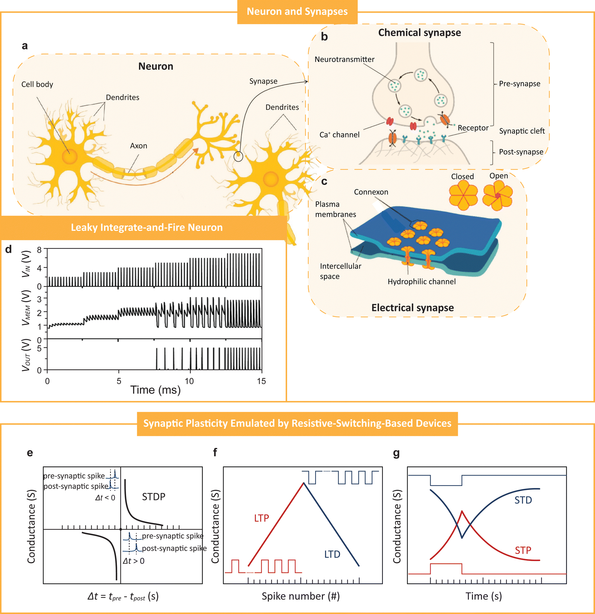 | ||
| Fig. 1 Building blocks of biological neurons and synapses. (a)–(c) Neurons and synapses including the basic structures of common neuron cell (a) and the synapses (b) and (c), where the chemical synapse (b) and electrical synapse (c) are responsible for signal transmission between neurons. (d) LIF neuron model. The neuron could fire a voltage spike after integrating several input voltage spikes and return to rest or off state. The input spikes (VIN) are expected to be larger than the operating threshold of the circuit to start the integration (VMEM) and generate the output (VOUT). (e)–(g), Synaptic functions: STDP (e), LTP and LTD (f), and STP and STD (g). For spiking-time dependent plasticity (STDP) in (e), the device conductance is modulated by the timing difference of input pre-synaptic spikes and the back propagation of post-synaptic spikes (insets of c), Δt. The larger Δt is, the smaller effect on the device conductance will be and vice versa. For long term potentiation and depression (LTP and LTD) in (f), device conductance changes with the consecutive input pulses (insets of f) and the initial, final, and intermediate states are stable. For short term potentiation and depression (STP and STD) in g, device conductance is modulated by a single or several pulses without permanent change on the conductance. Credits: (a)–(c) are reproduced under a Creative Commons Attribution (CC-BY) license; (d) is reproduced under Creative Commons Attribution (CC-BY) license from ref. 53, copyright Rozenberg et al. 2019 Springer Nature. | ||
In 1943, McCulloch and Pitts captured the accumulative function of the biological neuron that led to the eventual firing of an action potential into a mathematical model known as the McCulloch–Pitts neuron,1 which was the first spiking neuron model ever proposed. In 1952, Hodgkin and Huxley presented a comprehensive analysis of the dynamics of membrane potential under the concerted actuation of multiple ion channels.41 However, the resultant model, comprising several differential equations, is too complex. Some neuron modelling work, therefore, focused on simplicity, representing the overall function using lumped circuit components, e.g., the integrate-and-fire neuron42 (described by a membrane capacitance C) and improved leaky integrate-and-fire or LIF neuron43–45 (described by a parallel RC circuit). In the LIF neuron model, the shunt resistor R is used to account for the loss of ionic charge from the neuron in-between voltage spikes. Another noteworthy model is the adaptive exponential integrate-and-fire neuron,46–48 capable of describing numerous known firing patterns, e.g., bursting, delayed spike initiation, fast spiking, etc. A comprehensive review on different neuron models can be found in Burkitt et al.49
B. Basic function of the biological synapse
A von Neumann computer always requires the same amount of time to compute identical or similar data. In contrast, the brain is well known for its ability to learn and can subsequently process similar information in a much shorter time. Although the exact manner by which learning or cognition occurs in the brain remains an open question, this capability has been widely attributed to the synapses across which neurons communicate.39,50–52 During learning, it is believed that synaptic junctions throughout the biological neural network are selectively strengthened or weakened. This process creates a “memory map” comprising a subset of strongly connected neurons responsible for subsequent fast processing and propagation of similar data through the network.Synapses may be classified into two categories, namely chemical and electrical40 (Fig. 1b and c). At an electrical synapse, an incoming voltage spike creates a potential difference between the pre- and post-synaptic neurons and directly induces the flow of a sodium ionic current through the pores or intercellular channels that extend across the synaptic cleft54,55 (Fig. 1c). An electrical synapse can be either unidirectional or bidirectional and has a high transmission speed since the passive current flow across the gap junction is practically instantaneous. The purpose of electrical synapses is to synchronize the firing of a group of neurons to generate a strong stimulus that in turn triggers a crucial response, e.g., a lifesaving reaction. On the other hand, a chemical synapse responds to an action potential via the release of neurotransmitters. Unlike the electrical synapse, a chemical synapse does not have intercellular continuity across the synaptic cleft (Fig. 1b). When neurotransmitters that randomly diffuse across the gap junction are received at the receptor sites on the post-synaptic neuron, ion channels open to allow an inflow of sodium ions that in turn raise the membrane potential of the post-synaptic neuron. Due to the lack of direct transmission paths between the pre- and post-synaptic neurons, the response of a chemical synapse is much slower compared to the electrical counterpart.
Biological synapses modulate the flow of signals across the biological neural network and are believed to play the role of memory formation in the learning process.40 A strong synaptic connection between two neurons allows almost the entire action potential from the pre-synaptic neuron to be transmitted to the post. On the other hand, a weak synaptic connection suppresses the impact of an action potential on the post-synaptic neuron. Here, we outline a widely accepted theory, known as the Hebbian learning rule,56 which stipulates how the synaptic strength between neurons evolves during the learning process. This rule has thus far closely guided efforts in neuromorphic device development and may be summarized as follows. If a post-synaptic neuron fires a voltage spike after the pre, the latter is said to have directly influenced the depolarization of the former, and the synaptic strength is increased according to the time delay (Δt) between the two firing events (Fig. 1e). The increase is most significant when Δt ∼ 0, i.e., the post-synaptic neuron fires almost immediately after the pre. Conversely, the synaptic strength is reduced if the post-synaptic neuron fires before the pre, i.e., Δt < 0. These synaptic changes linked to the relative timing difference in the firing of the pre- and post-synaptic neurons are widely coined as spiking-time dependent plasticity (STDP).57–66
When there is consecutive firing of pre-/post-synaptic neurons, which may also be referred as excitatory/inhibitory spiking events, the synapse would progress towards long-term potentiation (LTP) or depression (LTD), as shown in Fig. 1f, respectively, for excitatory or inhibitory events, with the degree of the change depending on the time difference between the pre- and post-synaptic neuron spikes. In 1992, Dan and Poo proved in biological neuromuscular synapses that immediate and long-term depression happens when the postsynaptic pulses alone or the pre-synaptic spike is asynchronous, whereas synchronous pre- and postsynaptic spikes have no effects.59 To be precise, the synapse will be weakened if there are only post-synaptic spikes, or the pre-synaptic spikes happen only after the post-synaptic spikes. Such a biological observation was then confirmed by Debanne et al. in a hippocampal slice two years later.60 Afterwards, it was also found in rat hippocampal neurons that LTP happens if repetitive post-synaptic spikes occur within 20 ms of the pre-synaptic activation.62
Alternatively, when only one or a few such events happen, the STDP rule will simplify to short-term potentiation (STP) or depression (STD), as shown in Fig. 1g, which shows the change from rest potential to action potential and back to rest potential on neuron membranes, without persistent change in the synaptic strength. Therefore, the major difference between short-term potentiation/depression and long-term potentiation/depression lies in whether the synaptic plasticity is permanently changed during the spiking activities.
3. Strategies in current transition towards neuromorphic computing
ANN and SNN
The difference between existing ANN and emerging SNN should be addressed in the context of this review, due to the ambiguity of the terms used for describing them. As the name suggests, artificial neural networks include any neural network that is man-made, however, it should be made clear, as it has been introduced that SNN has established itself as the third generation of ANN because of its time-dependent spiking computational unit.18 Herein, in the context of this review, any artificial neural networks that are not spiking neural networks will be concluded as (traditional) ANN, and we separate the SNN for the ease of discussion. Fig. 2 adapted from ref. 67 elucidates the difference well. As shown in Fig. 2a, the inputs of ANNs are usually a vector X, with a vector weight gain W by a synapse multiplicator, then integrated and activated to generate the output. The inputs of the SNN, however, are unipolar time-dependent spike trains weighted by synapses and activated by neurons. The synaptic weighting and neuron activating in the SNN leverage on STDP and LIF, respectively, as described in the earlier section. Further difference in implementation is then illustrated in Fig. 2b that by using STDP, the time-dependent unipolar trains in the SNN are interpreted as the analogous weights stored in the synapses and then used for exciting or inhibiting the post-synapse neurons, in clear comparison to the ANN method that uses discrete numbers stored in the digital memory and computed by the arithmetic logic unit in the processor for countless multiply-and-accumulate (MAC) operations, followed by a non-linear activation for the final result.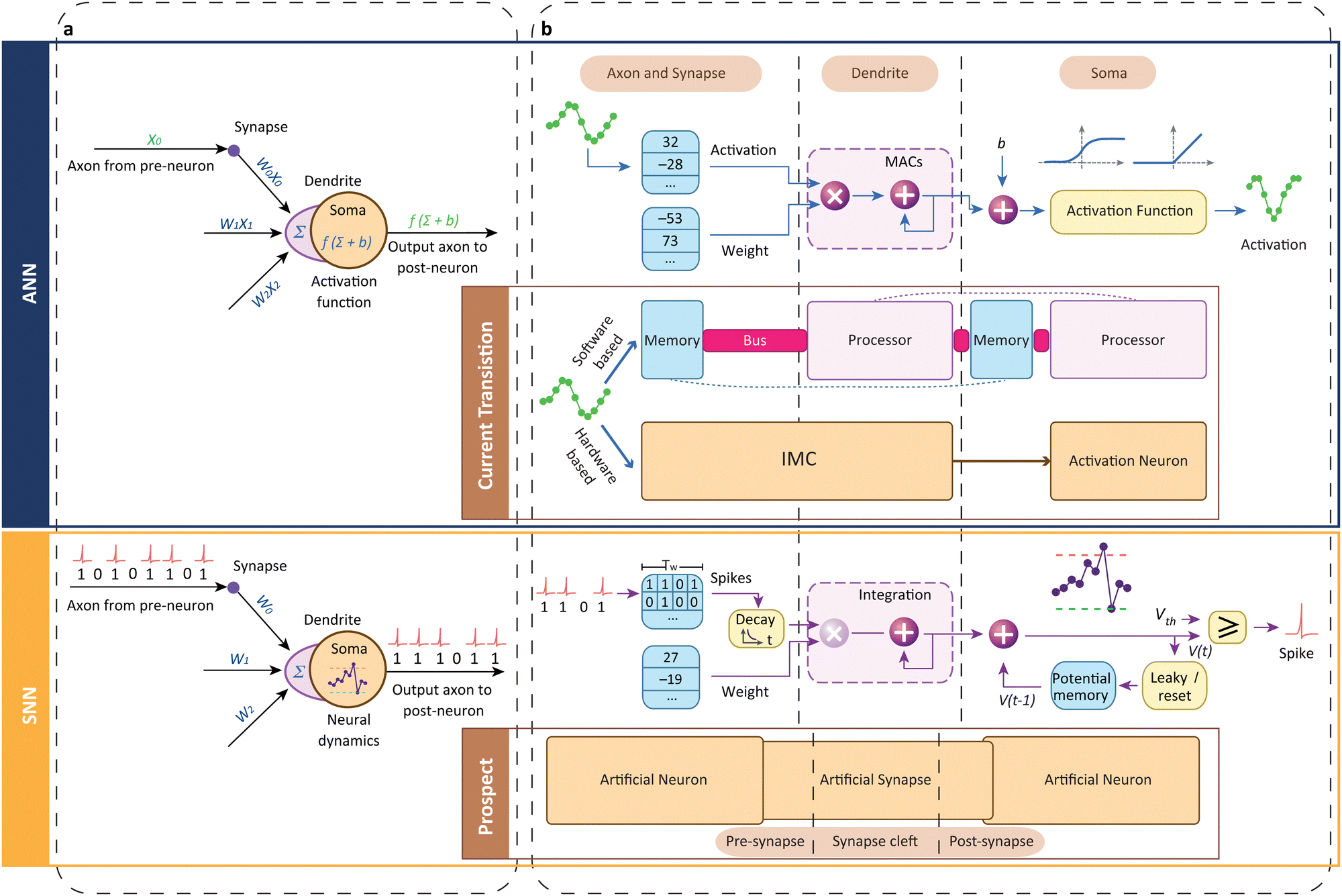 | ||
| Fig. 2 ANN and SNN: comparison and implementation. (a) Computational units of traditional ANN models and emerging SNN neuron models, where W denotes the synaptic weight, X denotes the input activation, Σ is the integration function, and f is the activation function. (b) Implementation of ANN and SNN neurons. ANN is implemented as a software algorithm with computational speed boosted using in-memory computing. SNN, on the other hand, requires emerging artificial neuron and synapse devices to function as time-dependent computing units. Credits: Adapted with permission from ref. 67, copyright 2019, Springer Nature. | ||
Neuromorphic computing is generally summarized as the electronic implementation of human-brain inspired computing. In the context of this review, neuromorphic computing, however, only refers to the SNN implemented by emerging synapse and neuron devices. The ANN has diverged from the perceptron so much that there is no similarity between the biological neural networks, except that it borrows some terminologies from biological neuron illustrated in the above sections. Furthermore, the physical level implementation of the ANN and SNN shown in Fig. 2b made the statement more clear. The existing software-based ANN is performed entirely on a processor with numerous data exchanges between the memory and processor, either or both of which is bottlenecked in the current development. The hardware-based ANN enabled by in-memory computing (IMC) extenuates the load of memory, processor, and the bus between them; therefore reduces the power consumption, accelerates the speed, and eases the burden of IC design. However, the hardware-based ANN emulates the brain's functionality in a way that there is no clear distinction between the memory and computing as the von Neumann architecture has. The basic operation resembles the software ANN still. Hardware SNN uses artificial neurons and synapses as the basic computational unit, in the most distinctive way that no actual numbers are passed between any part of the network except for unipolar spikes generated by neurons, which is the exact emulation of the biological neural network.
Hardware ANN: in-memory computing
Although they do not yet yield a complete neuromorphic system, in recent years, various notable hardware-based ANN approaches have been proposed for addressing the as-described von Neumann bottleneck.68–71 These approaches are primarily aimed at boosting computational speed (thus data throughput) by performing MAC, a typical unit of the CNN algorithm, within the memory storage. Known as the IMC approach, or the vector-matrix multiplication (VMM) machine shown in Fig. 3a and b, this computational method reduces the transfer of data between the processor and memory. For example, Sony's IMX500 intelligent vision system,72 announced in mid-2020, is a systems-in-package AI-vision solution that features a CMOS image sensor stacked on top of a digital signal processor customized for performing computation within the SRAM. The product offers two operational modes; a high-resolution picture mode for human viewing and an AI inference mode where the image is down-sampled and analysed using MobileNet at ∼3 ms per frame.72 Li et al. proposed an analogue spectrum analyser73 with a resistive random-access memory (RRAM) array. The input voltage signal with different frequencies (Fig. 3c) after multiplication with the conductance weights in the array could be transformed into a current signal that passes in certain cells (Fig. 3d). They performed 2D-discrete cosine transform (2D-DCT), an image processing/compression method to rearrange the pixels in the frequency domain, with their VMM machine to encode the image (Fig. 3e) and compare with the software (Fig. 3f), in which the distortion to human perception is negligible. Zidan et al., using a similar strategy, implemented an RRAM-based analogue Poisson equation solver.74 Likely, Oh et al. used RRAM to perform MAC and used Mott activation neurons75 to emulate rectified linear unit (ReLU) activation function to achieve edge detection of images.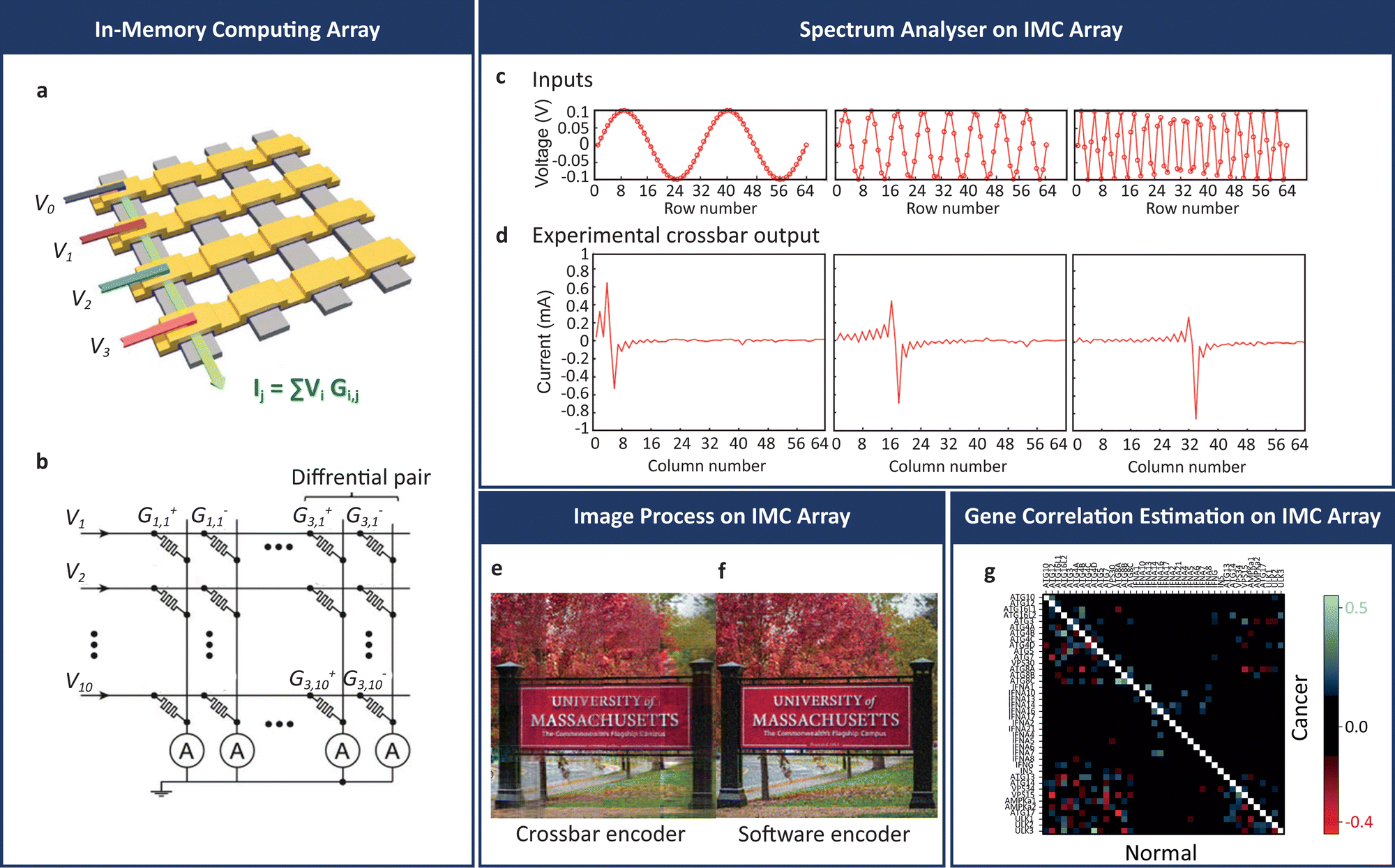 | ||
| Fig. 3 In-memory computing using a RRAM array. (a) Schematic of a RRAM array. The output current is the sum of several channels of voltage times the corresponding node conductance. (b) Schematic of the array with differential pair, where the differential output makes the array more robust. (c)–(f) Spectrum analyser using a RRAM array based on differential VMM, where with the input voltage signal (c) times the pre-programmed array weights, the array can output current at respective column expressing the frequency component of the input signals (d). With the functional hardware spectrum analyser, image encoding (two-dimensional discrete cosine transform, 2D-DCT) using a RRAM array (e) in comparison to the software encoder (f). (g) Gene correlation estimation on the IMC array. Partial correlation computed of 40 genes for cancer and normal tissues (only displayed correlation greater than 0.13 for visualization reason). Credits: (a) is reproduced with permission from ref. 74, copyright Zidan et al. 2018 Springer Nature; (b) is reproduced with permission from ref. 69, copyright Prezioso et al. 2015 Springer Nature Limited; (c)–(f) are reproduced with permission from ref. 73, copyright Li et al. 2018 Springer Nature; (g) is reproduced with permission from ref. 77, copyright Gallo et al. 2018 Springer Nature. | ||
Another IMC approach, proposed by Yao et al.,68 leveraged on the multiplicative and additive nature of Ohm's law and Kirchhoff's current law, respectively. It deployed a crossbar array of resistive memory cells wherein MAC computation was carried out. In an RRAM cell, the resistance or conductance of a sandwiched insulator layer can be modified electrically and the change is usually rendered non-volatile for storage application. In Yao's work, the resistances of RRAM cells in each crossbar array denoted the optimized weights of a CNN kernel derived from offline training. Image pixels were converted to corresponding voltages and applied to the RRAM cells to realize the CNN convolution, with the results represented by the summed current of the array. The computational performance was benchmarked against Tesla's V10076 GPU and more than two orders of magnitude better power efficiency and one order of magnitude better performance density were observed.
While most IMC applications focused on image processing, some unleashed MAC ability for the linear and partial equation solver. For example, Fig. 3g shows Gallo et al.'s work on 1 million PCM devices for a linear equation solver, used for partial gene correlation estimation in studies of cancer and normal tissues.
Admittedly, there are far more simulation works using RRAM for IMC than using physical arrays. However, the physical system is rather realistic, complicated, and interesting. Here, in addition to the above-mentioned works, Table 1 summarizes some of the on-array implementation of IMC using RRAM and FLASH and this may be useful for future inspiration.
| Work | Array size | Array type | On-array IMC (MAC/VMM) applications |
|---|---|---|---|
| a Size for Mott activation neurons. The edge detection was implemented by cooperating 32 × 32 Mott neurons with 16 × 16 RRAM synapses. | |||
| Berdan et al.70 | 5 × 5 | Passive | Linear multiplicator |
| Zidan et al.74 | 16 × 3 | Passive | Poisson equation solver |
| Li et al.73 | 128 × 64 | 1T1R | Spectrum analyser for image compression |
| Oh et al.75a | 32 × 32 | Passive | Activation neuron for edge detection |
| Sheridan et al.78 | 32 × 32 | Passive | Sparse encoding |
| Yao et al.68 | 128 × 8 | 1T1R | Hybrid CNN |
| Guo et al.79 | 785 × 128 | NOR-FLASH | MNIST classification |
| Yu et al.80 | 16 Mb | 1T1R | MNIST classification |
| Burr et al.81 | 500 × 661 | 2-PCM | MNIST classification |
| Gallo et al.77 | 512 × 2048 | 1T1R | Linear equation solver for partial correlation of genes estimation |
While the current innovative means of boosting computational speed have yielded a substantial improvement over the cloud- and GPU-based approaches, data sampling, movement and computation are still being controlled by a central clock speed, like those in a von Neumann system. This operational mode differs entirely from that of biological neural networks in the brain, which process sensory data in an asynchronous spike-driven manner, i.e., computations are triggered by changes in the data themselves. To attain the speed and energy efficiency of the biological counterpart, man-made systems must adopt a similar architecture and operating principle. A major research effort has been underway for nearly a decade to develop compact and low-power building block devices to realize this goal.
4. Neuromorphic building block devices
Building block devices for a neuromorphic computer must exhibit the basic characteristics of biological neurons and synapses. For artificial neurons, the internal variable must progressively build up according to the rate of the incoming voltage spikes and gradually dissipate in the absence of such spikes (i.e., the device should display a short-term memory). As for the artificial synapse, the internal variable must exhibit a continuum of non-volatile states that mimic the plasticity behaviour of the biological counterpart. Due to the significantly higher number of synapses (∼1015) compared to neurons (∼1010) in the human brain, size and energy consumption of artificial synapses are other key considerations that cannot be ignored in our drive towards a brain-like computer. In this section, we review some promising candidates, including the valence changing memristor (VCM), electrochemical metallization memristor (ECM), interfaced-controlled memristor (ICM), charge-trapping memristor (CTM), phase change memory (PCM), spin-transfer-torque memory (STTM), and ferroelectric tunnel junction memory (FTJM), with their pros and cons.A. Memristor
First predicted by Chua in 197182 but largely disregarded until the successful experimental demonstration in 2008,83 the two-terminal memristor is the fourth fundamental electrical component besides the capacitor, resistor, and inductor.82 A key characteristic of the memristor is the current–voltage hysteresis loop, which gives it a non-volatile resistance memory property. The memristor can be “programmed” to at least two distinct high and low resistance states (HRS and LRS), with numerous intermediate states possible through controlling the applied stimulation.83 Coupled with its structural simplicity which enables ultrahigh integration density in the form of a crossbar array, the memristor has been intensively studied in the past decade both as resistive switching memory or RRAM for post-flash tera-bit memory application and an artificial synapse/neuron for neuromorphic computing. The idea of memristors mimicking the dynamics of ion channels was theorized by Chua and Kang84 in 1976.Since the experimental validation of the memristor concept by HP Labs in 2008,83 many different memristive devices have been proposed and demonstrated (Fig. 4a–c). Generally, the physical mechanisms that govern resistance switching in these devices may be classified into the following categories, namely valence change memory (Fig. 4a), electrochemical metallization memory (Fig. 4b), interface-controlled memory (Fig. 4c), and charge-trapping memory (Fig. 4d).
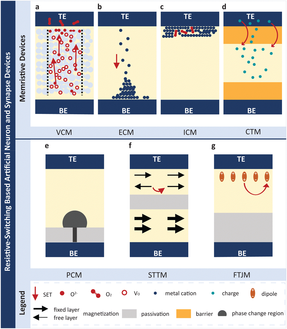 | ||
| Fig. 4 Resistive-switching-based artificial synapses and neurons. (a–g) are schematic of valence changing memristor (VCM, a), electrochemical metallization memristor (ECM, or namely conductive bridging memristor, b), interface-controlled memristor (ICM, c), charge-trapping memristor (CTM, d), phase changing memory (PCM, e), spin-transfer-torque memory (STTM, f), and ferroelectric tunnel junction memory (FTJM, g), respectively, where the red arrow indicates the set process. Credits: (a)–(g) are adapted from ref. 38 and 85–92. | ||
Zhang et al. used high-resolution transmission electron microscopy (HRTEM) to capture the filament evolution of a Pt/HfO2/Pt VCM device shown in Fig. 5a. Fig. 5b and c show HRTEM images (with fast-Fourier Transform (FFT) diffraction patterns) of devices operated at 0.1 mA compliance and 1 mA compliance, respectively, where crystalline hexagonal-Hf6O (h-Hf6O) is believed to be in the oxygen deficient conductive filament region and m-HfO2 to be the shell of the filament. To illustrate, Fig. 5d–k show the evolvement of the h-Hf6O filament from the pristine state (Fig. 5d) to be formed (Fig. 5e–g), shelled (Fig. 5h–j), and ruptured (Fig. 5k). The detailed mechanism, restricted by the scope of this work, may not be well elaborated. Dittmann et al. reviewed the VCM mechanism in detail120 where the engaged audience should refer to.
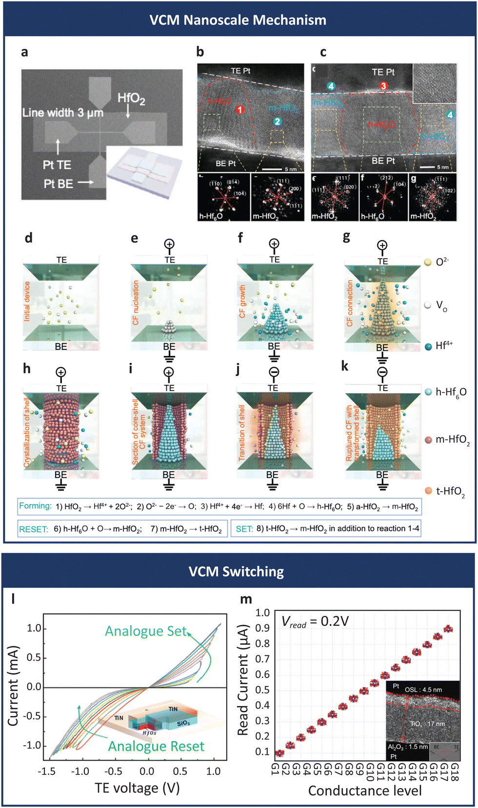 | ||
| Fig. 5 VCM nanoscale mechanism and switching for neuromorphic applications. (a) Device SEM image and schematic. (b) and (c), High resolution transmission electron microscopy (HRTEM) images of devices operated under 0.1 mA and 1 mA compliance current, respectively. (d)–(k), Illustrations of the evolvement of conductive filaments from forming to rupture. (l) Typical analogue set and reset cycle of VCM devices for neuromorphic applications. (m) Multiple conductance levels achieved by VCM devices for neuromorphic applications. (inset: TEM image of the device) Credits: (a)–(k) are reproduced under CC-BY licence from ref. 128, copyright Zhang et al. 2021 Springer Nature; (l) is reprinted from ref. 98, copyright 2020 American Chemical Society; m is reproduced under CC-BY licence from ref. 115, copyright 2022 Wiley-VCH. | ||
Many works present excellent analogue switching performance in D.C. mode without95,98,99,121 or with94,96,97,100,101,109,114,116 the help of compliance current, as shown in Fig. 5l. However, during set, the current usually increases abruptly due to heating that in turn accelerates defect generation.113,122,123 To suppress the thermal runaway, a series resistance that limits the current surge is required. This may be fulfilled by a selector device, typically a transistor, which also helps eliminate the sneak-path current problem in a crossbar array, which will be discussed in the following section. On the other hand, the current decreases gradually during reset because the migration of the O2− anions would be self-limited by the increasing thickness of the re-oxidized layer adjacent to the electrode.107,124 Sometimes, an oxygen reservoir layer,99,105,106,108,109,111,112,115–117,121 thermal enhancement or electro-thermal modulation layer (TEL/ETML),68,104,107,125–127 is adopted to mitigate such abrupt set behaviour. As shown in Fig. 5m, Kim et al.115 reported an alumina VCM device with a TiOy (y = 1.81) overshoot suppression layer (OSL) (inset shows its TEM image) and showed a conductance modulation within 20 nA error tolerance for 70 cycles.
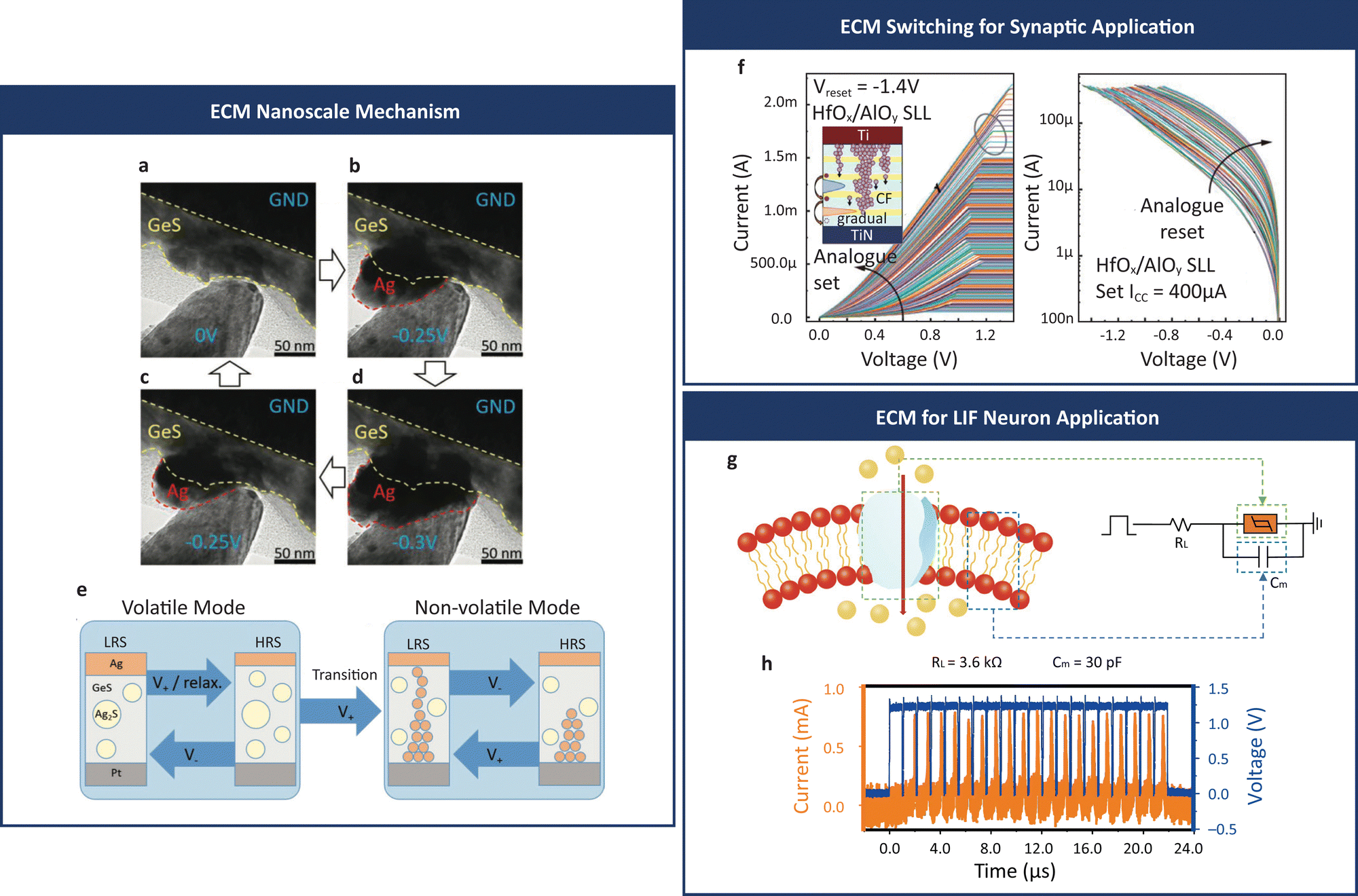 | ||
| Fig. 6 Electrochemical metallization memristor. (a)–(d), In situ TEM images showing Ag ion diffusion under a negative bias. (e) Illustration of the set/reset process of the GeS ECM device. (f) Analogue switching for synaptic application of HfOx/AlOy super-lattice-like (SLL) device. (inset: the schematic of SLL device) The analogue set is by setting different compliance currents, while the analogue reset is accomplished by setting different reset voltages. (g) Biological LIF neuron emulated by ECM with circuitry. RL and Cm denote load resistor and membrane capacitor, respectively. (h) Artificial LIF neuron response (current) to the input spike (voltage). Credits: (a)–(e) are reproduced with permission from ref. 134, copyright 2022 Kim et al., Wiley-VCH GmbH; (f) is reproduced with CC-BY licence from ref. 101, copyright Wang et al. 2022 Wiley-VCH GmbH; (g)–(h) is reproduced with CC-BY licence from ref. 142, copyright Duan et al. 2020 Springer Nature. | ||
Besides non-volatile switching, volatile or threshold switching is observed when the set current is capped below a certain value (usually on the order of microampere).140,141 In this case, the LRS is maintained over a limited voltage range only. When the voltage is decreased below a threshold value, the device reverts automatically to the HRS. The volatility is believed to stem from a relatively thin Ag filament formed under a limited set current.143 Furthermore, a more comprehensive review by Abbas et al. on ECM elaborated it well and accurately, which helps the understanding of this kind of device.143
Due to the high solubility of Ag, the thin filament readily “dissolves” when the excitation voltage is reduced. Exploiting this characteristic, several works142,144,145 made use of this behaviour to implement the integrate-fire function of a neuron. The circuit comprises a capacitor connected parallel to the threshold switch. When the capacitor is charged by input spikes to a voltage higher than the set voltage, the switch transits to the low-resistance state and discharges the capacitor. As the capacitor voltage decreases below the threshold, the switch transits back to the high-resistance state. The momentary discharge of the capacitor produces an output current spike. Duan et al.142 took this approach further by connecting 4 of such LIF neurons to 1 synaptic device to emulate the biological neuron and synapse illustrated in Fig. 15h.
For the synaptic operation, tuneable long-term potentiation and depression by varying spike amplitude,69,146 spike number,147 and spike rate141 are reported using non-volatility of ECM. With volatility, ECM shows also tuneable short-term potentiation by varying spike amplitude,134,146 spike rate,134 and spike number.134 It is worth mentioning that on a behavioural level, the ECM device is able to emulate Pavlov's dog experiment in simulation and can be developed for use in an addiction inhibition machine,148 thanks to its easy transition between volatile and non-volatile switching.
With the volatile switching characteristics, sometimes referred to as threshold switching (TS), ECM devices may be adapted for LIF neuron application, as illustrated in Fig. 6g. The biological neuronal membrane is emulated by the parallel capacitor (Cm) and the biological ion channel is emulated by the TS device, which shares more similarity to the conduction mechanism of ECM. Duan et al. used such a device with load resistor and capacitor showing LIF neuron characteristics discussed above, as shown in Fig. 6h142 and they also applied the neuron-synapse system for SNN simulation, more details of which will be provided in the following sections.
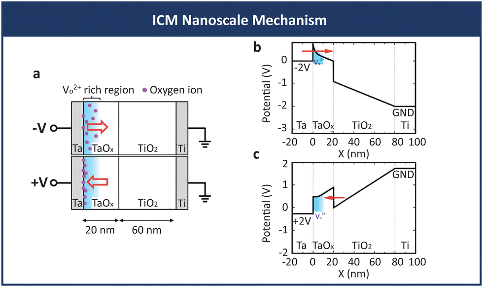 | ||
| Fig. 7 Interface-controlled memristor. (a) Illustration of the switching mechanism explained by a homogeneous barrier modulation model: oxygen ions migrate away from the oxygen vacancy-rich region at the Ta interface with negative bias (reset) increasing the effective barrier width for electron conduction and migrate towards that region with positive bias (set). (b) and (c), Energy band diagrams in LRS calculated at −2 V and 2 V read bias, respectively. Credit: Reproduced with CC-BY licence from ref. 88, copyright Wang et al. 2015 Springer Nature. | ||
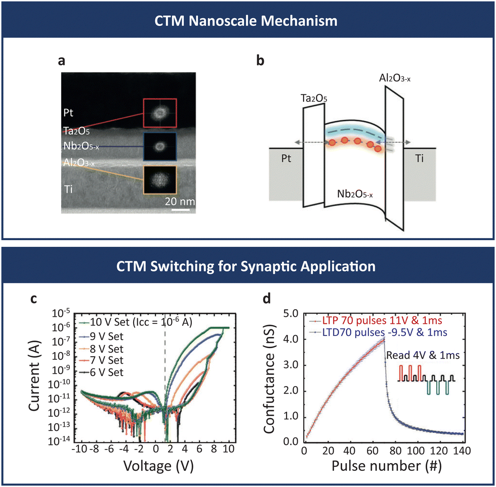 | ||
| Fig. 8 Charge-trap memristor. (a) Cross-sectional TEM image of the Pt/Ta2O5/Nb2O5−x/Al2O3−x/Ti device. Inset: FFT image of each dielectric layer. (b) Schematic energy band diagram shows the charge trapping mechanism of CTM. (c) Multi-level analogue set/reset. (d) LTP/LTD emulated by CTM device. Credit: Reproduced with CC-BY licence from ref. 92, copyright Kim et al. 2023 Wiley-VCH. | ||
Inherited from the charge trapping mechanism, a high programming voltage (∼10 V) might be one of the major obstacles in the neuromorphic application, which shall be enhanced in further studies.
B. Phase-change memory device
As the name suggests, phase-change memory (PCM) depends on thermally induced transition between the crystalline and amorphous phases as the mechanism for non-volatile resistance switching (Fig. 4e). A material widely studied for phase-change memory application is germanium-antimony-tellurium (GeSbTe or GST),161 by virtue of its ease of fabrication and low phase transition temperature. Meister et al. employed in situ TEM showing the resistance change at the nanoscale level of a GST PCM device, as depicted in Fig. 9a.162 It is shown in Fig. 9b that in the crystalline phase, GST has a low electrical resistance. Under short high-current pulsing, GST can be transformed into an amorphous phase having a much higher resistance (Fig. 9c), i.e., the reset of the PCM device. Selected area diffraction (SAD) of the red circle regions was carried out to confirm the polycrystalline and amorphous phases, as shown in Fig. 9d and e, respectively. Reversal to the low-resistance crystalline phase or the set process may be realized using a lower current pulse or a voltage pulse, but applied over a longer period. Shown in Fig. 9f, by applying 400 ns-varying amplitude voltage pulses, the device resistance changes gradually, which was further examined by TEM, as shown in Fig. 9g–i at the respective points, confirming the transition from the amorphous phase to crystalline phase during reset. In ref. 87, Wong et al. reviewed more basics and theories of phase change materials and devices to understand the mechanisms of PCM.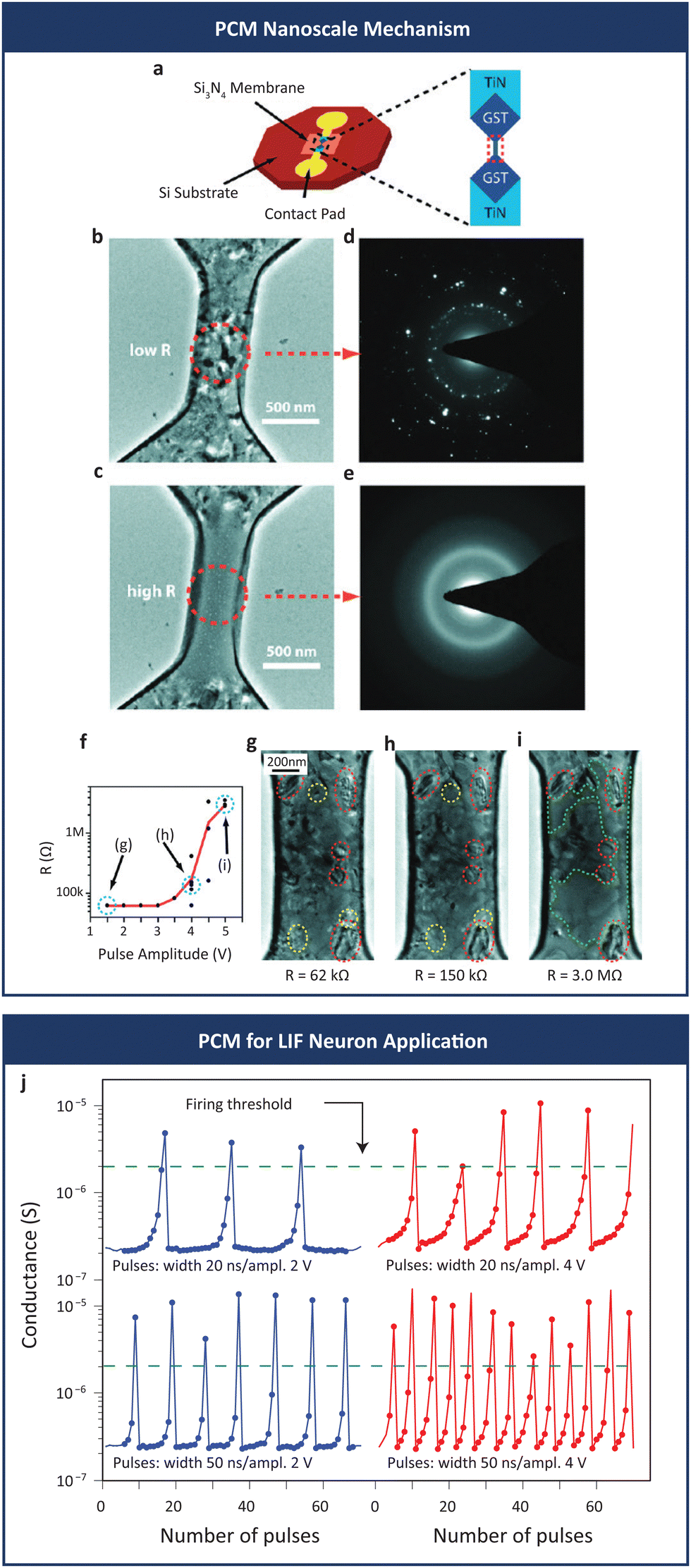 | ||
| Fig. 9 Phase-change memory device: nanoscale mechanism and LIF neuron application. (a) Device structure illustration. (b) and (c) in situ TEM images of PCM device in LRS and HRS, respectively. (d) and (e), Selective area diffraction (SAD) images of the circled regions confirming the amorphous and polycrystalline phases of (b) and (c). (f) Device reset by a 400 ns varying amplitude voltage pulse, at which the TEM images of the device are shown in (g)–(i), confirming the crystallization phase by the reset voltage pulse. (j) PCM device used for artificial neuron. Figure shows spiking rate and amplitude dependency of the neuron firing. Credits: (a)–(i) are reprinted with permission from ref. 162, copyright 2011 American Chemical Society; (j) is reproduced with permission from ref. 173, copyright Tuma et al. 2016 Springer Nature Limited. | ||
Through modulating thermal energy input, a gradual transition that yields multiple resistance states can be achieved, which has been exploited for synaptic emulation during numerous studies,163–171 where Suri et al. and Kuzum et al. were the first to use PCM as an artificial synapse.163–168 Thanks to PCM devices’ gradual phase transition by the Joule heating effect and stable phase physics, PCM shows great potential in multi-bit storage with long retention time. This stability gives many benefits in long term memory: PCM synapses show excellent tuneable LTP by adjusting voltage or current pulse width,166,168 amplitude,171,172 and rate (duty cycle).165–167 Tuma et al. also used a PCM device for artificial neuron application, as shown in Fig. 9j. The artificial LIF neuron shows a tuneable firing rate depending on the spiking rate and amplitude.
However, the phase change induced by the Joule heating effect is non-linear. A typical milli-seconds to seconds interval between set pulses is adopted to prevent over-heating with pulses,163,166,167,170,174 which is detrimental to the high-speed operation of the device. Another problem brought together by Joule heating is the power consumption that despite the fact that the technology node of PCMs has shrunk down to 40 nm diameter,172 the action energy consumption for pulse operation touches the bottom at the pico-Joule level.87,163,165,170–172
C. Spin-transfer-torque-based device
As a class of magnetic random-access memory (MRAM) devices, spintronic devices have emerged as potential candidates for emulation of neurons and synapses.175 The major difference between MRAM and non-MRAM is the storage media: the magnetic memory uses magnetization for the data storage, while the non-magnetic memory uses electrons or defect states. As shown in Fig. 4f, the typical structure of a spin-transfer torque cell is a sandwiched structure of one non-magnetic layer in between two nanomagnetic layers, of which one layer has fixed magnetization Mfixed and the other has free magnetization Mfree. When the current is injected into the stack, the spin torque will rotate Mfree and thus through the magnetoresistance effect change the resistance of the device.89 Spin torque can either rotate Mfree towards or away from Mfixed, depending on the polarity of input current, whose density also determines the amplitude of spin torque.176,177 An ideal value of input current is ∼40 μA under 22 nm CMOS technology.178 A parallel state (P state) is hence achieved when magnetizations of the free layer are paralleled with the fixed layer and an antiparallel state (AP state) is achieved vice versa. The SET and RESET processes are induced by sweeping positive and negative D.C. currents, respectively. Since spintronic devices are magnetization-based, it is not straightforward to include them in our benchmarking scheme. Therefore, we will discuss briefly the merits and challenges here. For the audiences who are engaged in this field, a detailed review on neuromorphic MRAM by Shao et al.179 is provided.In 2014, Vincent et al.180,181 used a spintronic memristive device to simulate neuromorphic computing ability. It is found that a spintronic device has stochastic switching180–184 and transiting185,186 nature, so the device functions binarily. Recent reports proposed novel-structured spintronic devices187,188 to achieve continuous potentiation/depression by tuning hall resistance.
From the discussion on device physics, the biggest merit of MRAM lies in its non-volatility, i.e., long retention, high endurance, and compatibility for front-end-of-line CMOS fabrication.189 Thus, commercialized MRAM chips have been fabricated189 for their capacitor-less high-density potential. However, it is also reported that spintronic devices are inherently prone to bit errors due to thermal activation,175 consume large operating power,187,188 use complicated structure,190 and require circuitry191 or extra components188 for the conversion between the electrical signal and magnetic states, which may challenge the device application.
D. Ferroelectric tunnel junction device
First discovered in 1920,192 ferroelectricity is a phenomenon where the electrical polarization of a material can be reversed by applying an external voltage, showing a hysteresis curve. Ferroelectric materials are extensively demonstrated and commercialized in non-volatile random-access memory (NVRAM).193–195 As for artificial neuron and synapse applications, ferroelectric tunnel junction (FTJ) devices are introduced here. As shown in Fig. 4g, as the polarization of the ferroelectric nanolayer changes, the polarization charge effect induces asymmetrical barrier heights.196,197 While with the polarization points downward, the barrier height reduces to Φ- (LRS) and the barrier height increases to Φ+ when the polarization directs upward (HRS). Since tunnel transmission is determined by the square root of the barrier height, the junction resistance is hence dependent on the barrier height.91 To investigate the switching in nanoscale mechanisms, Chanthbouala et al. employed piezoresponse force microscopy (PFM), as shown in Fig. 10a during positive (red) and negative (blue) voltage sweeping. Starting from the LRS, the device shows homogeneously up-polarized states and gradually transits to mostly down-polarized states with PFM showing the nucleation and expansion of down-domains under positive pulses of increasing amplitude. In contrast, negative pulses with increasing amplitude result in the nucleation and expansion of up-domains. Typical ferroelectric dielectrics used in FTJ for neuromorphic application are BaTiO3 (BTO),198–202 BiFeO3 (BFO),91,203,204 ferroelectric Hf0.5Zr0.5O2 (Zr-doped HfO2, FE-HZO),205–208 and HfSiO (Si-doped HfOx).70 For more ferroelectric materials and mechanisms, a rather interesting review by Mikolajick et al. may help with the understanding of ferroelectric materials and devices.209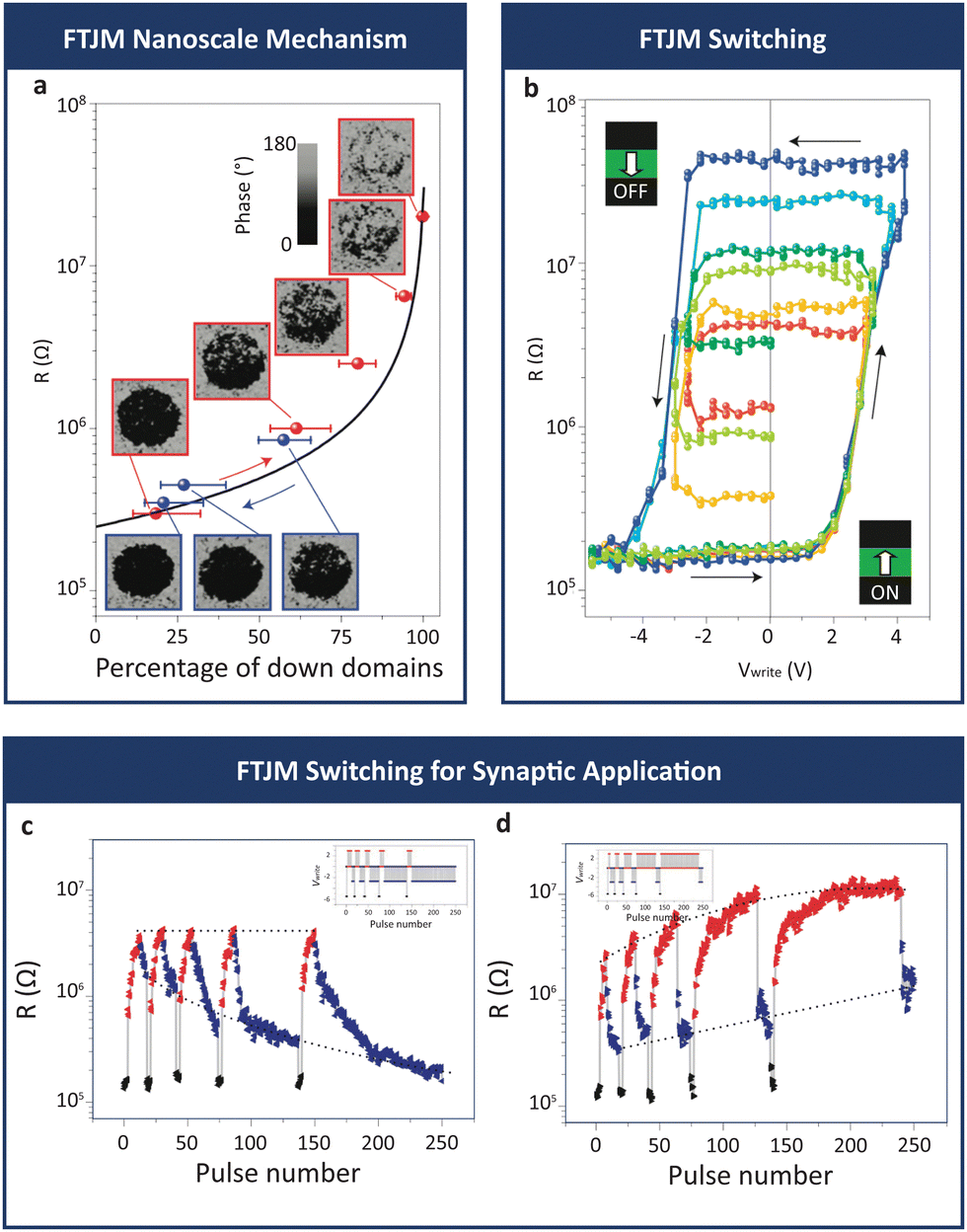 | ||
| Fig. 10 Ferroelectric tunnelling junction device for neuromorphic application. (a) Piezoresponse force microscopy (PFM) images captured during applying increasing positive (red) and negative (blue) voltage pulses. (b) Tuneable FTJ device switching characteristics with different write voltages. (c) and (d) Tuneable FTJ potentiation and depression by varying reset pulse number (c) or set pulse number (d), where insets show the pulse scheme. Credits: Reproduced with permission from ref. 198, copyright 2012 Chanthbouala et al. Springer Nature Limited. | ||
The first BTO FTJ device reported by Chanthbouala et al.198 exhibits a gradual switching with a good on- to off-ratio (∼103), as shown in Fig. 10b. Their work also shows the device tuneable potentiation and depression ability by applying consecutive identical pulse trains varying the number of depression (Fig. 10c) or potentiation pulses (Fig. 10d). Later, Ryu et al.206 reported a HZO FTJ device with a gradual polarization change in hysteresis thus enabling a better potentiation and depression in synapse application.
E. Memcapacitor
The memcapacitor has been recently reported210 and used for neuromorphic applications and has almost symmetrical and linear LTP/LTD. Physics of a memcapacitor are rather simple: the capacitance of memory dielectrics is modulated by the applied field in a 4-terminal structure, while memory dielectrics are commonly ferroelectric materials or charge trapping materials. With the appropriate programming gate voltage (memory window), the charges or fields are trapped or fixed in the dielectrics by a charge shield formed in the n− region. The device states are read out from the bottom electrode when applying a biased alternating voltage on the gate.210 However, the device needs complex circuitry to read out device states due to the capacitive nature. Also, benchmarking for this emerging type of electronics is not straightforward as compared to the resistive kind of device: although the capacitor consumes ideally no energy during the operation as it only involves the storage of charges rather than electro-conduction, in the neuromorphic application, the energy carried by the spikes shall be stored, or consumed within the device to program the capacitive states. Therefore, the performance is characterized in a similar manner to the rest of the devices.5. Universal benchmark of artificial synapse and neuron devices
So far, seven basic types of resistive switching-based electronic neuron and synapse devices and their switching mechanisms have been discussed. Behind the obvious mechanism, devices perform differently: some with large switching ratios, some with faster switching speed, some with better potentiation/depression linearity, some require large voltages, some require long pulse intervals, some are flexible, some are CMOS-compatible while some are not, and so on. There is thus an urgent need for providing a benchmark that is straightforward and universal to locate the device by its performance intra- and inter-device groups. By considering the needs and the physics of emerging neuromorphic devices, we find the energy/power consumption becomes a suitable candidate for its universality, i.e., can be applied to any devices that require electricity to operate. Precisely speaking, we adopt the spike voltage (or current for some phase changing synaptic devices), LRS and HRS conductance, and spike timing used in spiking potentiation and depression for the energy and power benchmarking.A. Benchmark for artificial synapse devices
A benchmark for synapse devices is provided in Fig. 11a and b. To describe the data, the action energy and standby power are defined using eqn (1) and (2), respectively.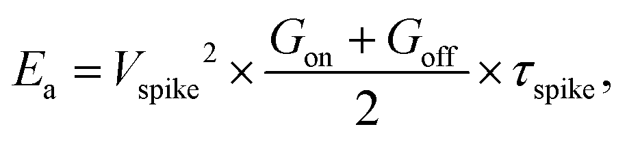 | (1) |
| Ps = Vspike2 × Goff, | (2) |
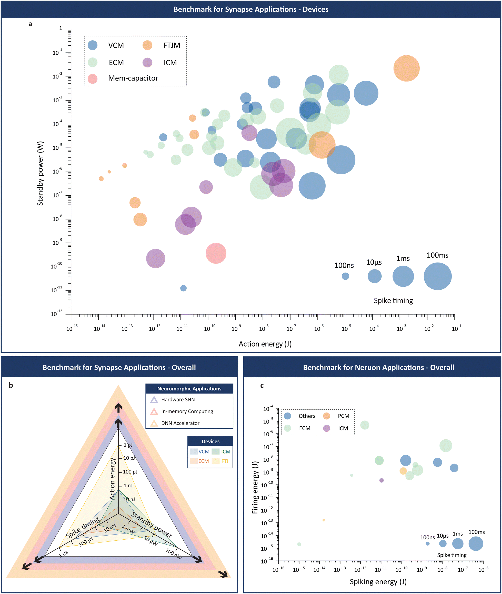 | ||
| Fig. 11 Universal benchmark for artificial synapse and neuron devices for valence changing memristive device (VCM), electrochemical metallization memristive device (ECM), interface-controlled memristive device (ICM), ferroelectric tunnelling junction device (FTJM), and mem-capacitor. (a) Benchmark for synapse applications, where standby power is a function of action energy and the diameter of the bubble indicates the spike timing of the device. (b) Overall performance comparison of artificial synaptic devices based on the median of each device group in the benchmark. The outer frame suggests possible neuromorphic application direction. (c) Benchmark for neuron applications, where firing energy is a function of spiking energy. Credits: VCM data are extracted from ref. 94, 95, 97, 98, 100, 102–108, 114–116, 124–126 and 213–220, ECM data are extracted from ref. 69, 122, 123 and 220–228, ICM data are extracted from ref. 88, 149–154 and 229, and FTJM data are extracted from ref. 70, 198, 200, 204–207, 230 and 231, mem-capacitor data are extracted from ref. 210, and artificial neuron data are extracted from ref. 142, 173 and 232–243. | ||
![[thin space (1/6-em)]](https://www.rsc.org/images/entities/char_2009.gif) 000 neurons.211 The higher the standby power of the synaptic device, the higher the chance of misfiring and the combined leakage current of 10000 neurons can be disastrous.
000 neurons.211 The higher the standby power of the synaptic device, the higher the chance of misfiring and the combined leakage current of 10000 neurons can be disastrous.
Further analysis of ECM devices in Fig. 11a and b shows reasonable standby power (median ∼ 56 μW) as compared to its worst action energy (median ∼ 13 nJ) between classes. Despite ECM typically having a bigger memory window, the high current used to stabilize the metal filament may cause a high action energy in the synapse application. However, efforts have been made to reduce the action energy to the pJ level. Different from VCM, enhancement of ECM centres on the manipulation of the cation conduction channel. Remarkably, the authors of ref. 225 used a 2 nm Mo/Ti or Ti barrier layer to buffer the diffusion of cations, reducing the action energy consumption to 2 pJ and a similar cation barrier HfOx/AlOy superlattice-like structured device was used in ref. 101, shown in the inset of Fig. 6f, to lower the action energy to tens of picojoules. Additionally, the optimized anion migration helps greatly with the linearity in potentiation and depression to 1.44 and 2.55. The authors of ref. 244 used tellurium (Te), an elemental small band gap semiconductor, as the anode to reduce the 1-atom conductance from 80 μS to 2.4 μS and thus reduce the 1-atom program energy to 0.2 pJ and action energy for potentiation to 140 pJ. Similarly, the authors of ref. 122 used less-diffusive tantalum (Ta) as the anode, which form, the authors of a more controllable conductive channel to make potentiation and depression fast to 100 ns spike to achieve better energy performance (81 pJ). Following this path, the authors of ref. 147 used epitaxially grown SiGe in which a conduction channel enabled by dislocations was selectively etched and widened to form an even better controlled conduction channel. By confinement of the conduction channel in the selective-etched region, not only the standby power is suppressed to 1.5 μW, but also its cycle-to-cycle and device-to-device (different etching batches) variation is stressed to less than 1% and 4.9%, respectively. However, most devices may suffer from high action energy to achieve a stable resistance state, from visualization in Fig. 11b. Thus, instead of trying to use it as a viable candidate for synapse application, ECM is better suited for neuron applications due to its easy transition in volatility and assembly to biological neuron models, as described in Fig. 6g and will be covered in the following discussions.
For interface-controlled synaptic device performance analysed in Fig. 11a; they have much lower action energy and standby power than valence change or electrochemical metallization devices. This is attributed to the low action/rest current of the device stack, which forms no conductive channel and is fully modulated by the resistance change of the interface between the electrode and the PCMO layer or between two oxide layers with different stoichiometry during resistive switching. However, the resistance modulation mechanism that helps with energy consumption is not helpful to the spike timing. Due to the slow redox reaction at the interface, the median of spike timing is up to milliseconds, as compared to the μs level timing of non-chemically reactive synaptic devices. On the other hand, interface-controlled devices are much more capable for the continuous signal with a small dynamic range and a low fresh rate, thanks to their low standby power and action energy, resulting from the oxygen interchange between the two layers, which modulates the interface conduction barrier only.104,107,125,218 Therefore, with the low standby power and moderate action energy among the classes, ICM is recommended for DNN accelerator applications, where rare updating and frequent reading are required, refer to Fig. 11b.
From an energy budget perspective, most benchmarked FTJ synaptic devices outperform the rest of the devices, as shown in Fig. 11c. And one excellent HZO FTJ device207 stands out even at 10 femtojoule per spike, thanks to its ultra-thin switching layer (3.5 nm) with a metallic oxide electrode (WOx), which helps with a much lower barrier and also contributes to ohmic conduction, allowing an enwidened hardware VMM application range. And thanks to its all plasma-enhanced atomic layered deposition (PE-ALD) fabrication process, the device shows 10 billion write–erase cycle endurance. As suggested in Fig. 11b, FTJ devices are potential candidates for in-memory computing applications discussed in the opening sections, for their fast spike timing and low action energy that can be adapted for frequent and fast updating of the synaptic weight requirements.
As an emerging device, the memcapacitor device consumes low standby power and moderate action energy, as shown in Fig. 11a. Although it is a promising candidatefurther analysis and comparison has not been possible to date due to the limited reports on this kind of device. More investigation is encouraged to enrich the research in this area.
B. Benchmark for artificial neurons
A benchmark for artificial neurons is provided in Fig. 11c. Unlike the case of synapse which can be emulated by a single device, most artificial neurons have external circuitry, accompanied by a source resistor, a parallel capacitor for charging and discharging during the refractory period, and a load resistor. Some are even equipped with an amplifier. It is not fair to compare a device connected only to a load resistor with a device equipped with a complex circuit with an external power supply (for amplifier), even if some reports argued that their stand-alone device is power efficient. Therefore, to ensure fairness, benchmarking here refers to the net power consumption used in the neuron system, not just the device itself, as defined by the spiking energy and firing energy in eqn (3) and (4), respectively.| ES = Vspike2 × Goff × τspike, | (3) |
| Ef = Vspike2 × Gon × τspike, | (4) |
Besides ECM neurons, some used ICM devices,242 PCM devices,173,243 Si nanorods,232 mixed-ionic conduction devices,239 and van der Waals heterojunction devices.238 It is rather worth mentioning that instead of avoiding the discussion of stochasticity of artificial neurons, Tuma et al. exploited the stochastic nature of PCM neuron devices.173 Since they found that cycle-to-cycle variation followed the normal distribution, a population code was introduced using the quantity of neuron devices to compensate the stochasticity of the neuron, especially in the occasion when input spikes were at high-frequency. With this method, the system robustness was increased. Besides, their neurons consume low firing and spiking energy because of the well-investigated spike timing-interval dependencies, indicating a possible path to overcome the energy consumption issue of most artificial neurons.
6. Challenges, guidelines, and outlooks
Although neuromorphic devices and computing are a revolutionary and promising technology, their development is still in its infancy. However, lots of efforts have been made to pave the road for it by many researchers in every possible direction. In 2022, a more envisionary roadmap on neuromorphic computing and engineering was proposed by leading scientists in their fields to discuss the insightful perspectives, where the engaged audiences may refer to. Here, based on our benchmarking data, we provide some useful insights on device level challenges, design guidelines, and an outlook.245A. Challenges
Although many papers reported artificial synapses and neurons made of resistive switching-based emerging devices in the last decade, ANN performance was usually illustrated through simulations based on device measurement data. There have been several reports on array-level work,70,147,246 but none matched the performance of current GPU-based systems. The first system-level implementation with performance exceeding that of the GPU counterpart was made by Yao et al.68 in early 2020. The delay in the device to array implementation may be ascribed to two major challenges.The first is variability, Fig. 12 shows the statistics of variation problem, both device-to-device (inter-device variation) and cycle-to-cycle (intra-device variation) for a given device structure. This problem is particularly severe in memristors that depend on the formation and rupture of a conducting filament as the basis for resistance switching. For example, Mahadevaiah et al.110 reported the current variation in a 64 by 64 packed VCM array after forming, where the variation is random overall and deterministic in a certain region, which might be contaminated during fabrication.111 They also explored the cumulative probability of devices’ current after the 1st, 10th, and 100th set and reset pulses over 100 devices, showing a wide and stochastic distribution of the pulse (A.C.) operation.111 Such a problem can be caused by intrinsic properties of the switching material. As shown in Fig. 12a–c, by changing the switching material, the distribution of LRS and HRS current is improved over cycles and among 1000 devices.172 The stochastic nature of filament formation and rupture, exacerbated by manufacturing-induced jitters, has caused a significant variation of programmed resistance values used to represent the weights in the ANN. Random variations in weights have been shown to negatively impact network's learning and prediction accuracy111,171,172,247 because with the intra-device variation, the resistance can sometimes overlap with each other, causing inaccurate weight storage. This is worsened by the superposition effect of the inter-device variation for the array level application, as shown in Fig. 12d. As shown in Fig. 12e and f, for a 5-level storage device, the probabilistic density function (PDF) of the current overlaps after temperature retention, which causes the disturbance in training and testing of a two-layer neural network, dropping from 82.6% accuracy to 72% in the MNIST database.172 As compared to the results from fresh samples shown in Fig. 12g, the confusion matrix of the testing results in Fig. 12h clearly shows the compromised results. The problem also renders online network training impractical. Training is carried out offline via simulation and then the optimized weights programmed into the memristor array. On the other hand, the issue is less severe in interface-controlled memristor devices because of the better resistance modulation in a small dynamic range, as analysed in the benchmarking. For instance, Yao et al.68 used an ICM device and demonstrated through discussion of its physics that devices’ resistance states are only modulated between the interfacial layers given good control and stability and therefore suitable for hybrid training (baseline weights obtained offline and updating online) a CNN accelerator and achieved 3.81% final test error in the MNIST dataset.
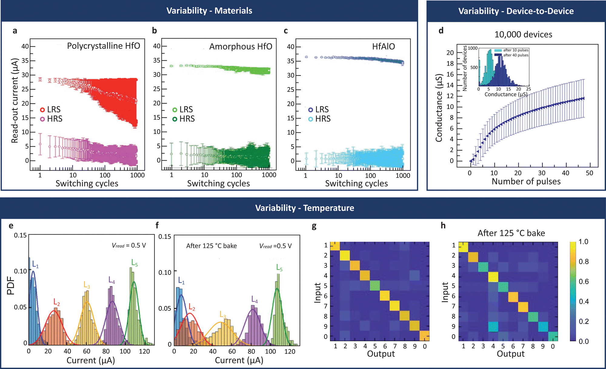 | ||
| Fig. 12 Challenges in variability. (a)–(c) Variability caused by materials on device-to-device over cycles statistics: pulse (A.C.) endurance test for 1000 devices with different switching materials, i.e., pHfO for polycrystalline hafnia (a), aHfO for amorphous hafnia (b), and HfAlO for hafnium aluminium oxide (c) (|Vset| = 1.2 V, |Vreset| = 1.8 V). (d) Device-to-device variation on over 104 PCM cells with 50 consecutive potentiation pulses (tpulse = 50 ns, Ipulse = 100 μA) operation. The inset of (d) shows device conductance distribution after 10 and 40 pulses, both shapes’ normal distributions. (e)–(h), Temperature instability for multibit operation: e and f, current probabilistic density functions read at 0.5 V before (e) and after (f) 125 Celsius degree baking, where the latter shows a significant overlap between current states between the states. (g–h) Confusion matrix on MNIST classification results before (g) and after (h) 1 hour annealing, accuracy drops from 86.5% to 72% after 125 Celsius degree baking. Credits: (a)–(c) and (g), (h) are reproduced under CC-BY licence from ref. 111, copyright Milo et al. 2019 AIP Publishing; d is reproduced under CC-BY licence from ref. 172, copyright Sebastian et al. 2017 Springer Nature. | ||
The other challenge lies in the sneak path current in a passive crossbar array and the lack of a compact, reliable selector or access device to suppress it. A sneak path current is a parasitic current added, by neighbouring memristors in the low-resistance state, to the read current of a memristor in the high-resistance state thus giving rise to a wrong read-out value. The typical way to solve this problem is to isolate memristors from one another using access transistors,169 like in the current dynamic random-access memory. However, doing so erodes the high integration density and process simplicity advantages of the crossbar architecture. Some researchers have proposed threshold or volatile switching devices with the same structure as memristors as potential selector devices.214,248 The sneak path current issue has on the other hand motivated the development of memory transistors, which combine both the select and memory functions in a single device.
Another issue with memristors lies with the implementation of the STDP learning rule, which is crucial to the operation of SNNs. As shown in many papers,140,249 shaping and overlapping of voltage waveforms at the two terminals are required to achieve the desired outcomes. This adds substantial complexity to the design of supporting circuitry. To date, system-level implementation of SNNs based on memristors has not been demonstrated.
B. Guidelines
From the proposed benchmark and the analysis of a tiny corner of the publications, we screen out several pathways for low-energy consumption, high-speed, and highly robust artificial neuron and synapse devices towards the neuromorphic electronics era. Here, useful insights on the statistical data regarding memristive devices are provided.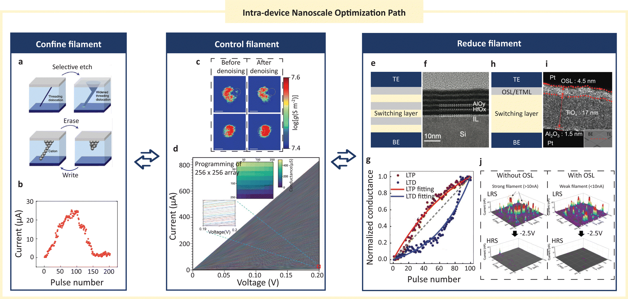 | ||
| Fig. 13 Intra-device nanoscale optimization path for neuromorphic applications. (a) Selective etching of epitaxial SiGe to form a channel for metal filaments. (b) Long-term potentiation and depression of the epi-SiGe devices, showing good linearity. (c) C-AFM images of the Ta/Ti/Al2O3/HfO2/Pt device before and after using a custom denoising write-verification pulse program, showing a better control filament using such a pulsing scheme. (d) The 2048 conductance states obtained from fine conductance tuning of the device in (c). (e) Device with multiple repeated switching layers, or superlattice-like (SLL) structure, TEM image of such a structure is shown in (f). (g) Enhanced long-term potentiation and depression achieved by the SLL device in (f). (h) Device with overshoot suppression layer (OSL) or electro-/thermal modulation layer (ETML), TEM image of such a structure is shown in (i). (j) C-AFM image comparisons of the device without OSL and with OSL in LRS and HRS, confirming the reduced filament size in OSL devices. Credits: (a) and (b) are reproduced with permissions from ref. 147, copyright 2018 Choi et al. 2017, under exclusive licence to Macmillan Publishers Limited, part of Springer Nature; (c) and (d) are reproduced with permission from ref. 212, copyright 2023 Rao et al. under exclusive licence to Springer Nature Limited; e is adapted from ref. 104, 107, 115, 125, 214 and 218; (f) and (g) are reproduced under CC-BY licence from ref. 101, copyright Wang et al. 2022 Wiley-VCH GmbH; h is adapted from ref. 94, 101 and 225; (i) and (j) are reproduced under CC-BY licence from ref. 115, copyright Kim et al. 2022 Wiley-VCH GmbH. | ||
Another major optimization path is to reduce the filament by material designing. Here two designs of memristive neuromorphic devices with common feature are stressed: conduction engineering (Fig. 13e and f) and electron/thermal (barrier) modulation of filaments (Fig. 13h and i). Firstly, from Fig. 11a, the energy consumption per spike for different devices spreads from tens of femto-joules to hundreds of milli-joules. It is obvious that Joule heat contributes most besides the energy used for switching since there are no light, sound, or haptic emission during switching. Thus, to control heat generation is one of the most important ways to reduce energy consumption, especially action energy. One approach is to create a potential barrier by introducing multiple layers to slow down filament migration (Fig. 13e)94,101,225 or using less diffusive filaments as the electrode.122,244 The benefit of multiple repeating layers reflected in the good linearity of potentiation and depression, as shown in Fig. 13g. Another design is to introduce a single modulation layer to mitigate the filament formation and rupture (Fig. 13h). Among materials used in the benchmarked devices, TaOx,104,107,125,218 TiOx,115 and VOx214 are investigated and reported to have such functions. As shown in Fig. 13i, they function as the overshoot suppression layer by modulating the conductive filament diffusion, which is also a key factor to reduce the action energy, increase linearity of synapse potentiation and depression and to lower the standby power. Rao et al.'s work also adopted a similar approach using nanometre thin Al2O3 and Ti functioning as an electro/thermal modulation layer to help with filament control.
In complete contrast, non-filament switching layers are used to suppress the conduction of electrons/vacancies and heat.149,150,153,154 Good energy control of ferroelectric and spintronic devices can also be attributed to the same reason that switching is modulated by using the potential difference of electron dipoles and different orbits of magnetization, allowing no actual filament conduction inside the device, which ultimately results in little Joule heat generation.
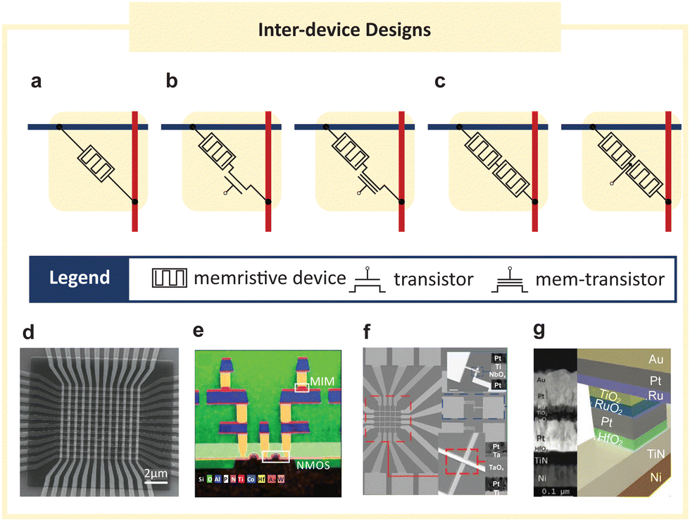 | ||
| Fig. 14 Inter-device designs: (a) passive crossbar structure (SEM image of a 10 by 10 memristor array is shown in (d). (b) active crossbar structure, the pass transistor or selector offers the third terminal to these configurations, where the pass transistor or selector could be a traditional field effect transistor, whose SEM-EDX image is shown in (e), or ferroelectric field effect transistor. (c) series memristors, typically with (right) the inter-device's third terminal, which can be in planar structure and connected by interconnects (SEM shown in (f), where the upper inset is the NbOx memristor and the lower inset is the TaOx memristor, with their respective TEM images) or vertically stacked (TEM images and schematic shown in (g)). Credits: d is reproduced with permission from ref. 69, copyright Prezioso et al. 2015 Springer Nature Limited, e is reproduced under CC-BY licence from ref. 111 copyright Milo et al. 2019 AIP Publishing; f is reproduced under CC-BY licence from ref. 142, copyright Duan et al. 2020 Springer Nature; and g is reproduced with permission from ref. 248, copyright Woo et al. 2022 Wiley-VCH GmbH. | ||
Active and passive crossbars. As shown in Fig. 14a and b, the crossbar (cross-point, x-bar) configuration comprises the device(s) connected by two perpendicular electrodes. No matter whether active or passive, crossbar connection makes large scale integration of memristive neuron or synapse devices possible and requires a CMOS-compatible fabrication process, which brings more challenges in variation control in deposition, lithography, etching, etc., especially for emerging materials. No pain, no gain; nevertheless, the complex and high-standard fabrication trades off for more opportunities.
Passive crossbars progressed slowly since the first validation of the passive crossbar idea by Prezioso et al. on a 10 by 10 array (Fig. 14d)69 because of the sneak path challenges of the passive crossbar, as elaborated in the above sections. In our benchmark, standby power metrics show the potential of a device to minimize sneak path current. Particularly, standby power of FTJ and interfaced-controlled memristive devices is significantly lower than that of the others shown in Fig. 11c, which facilitates their potential in passive array application: a 5 by 5 FTJ array built by Berdan et al. showed that the VMM error of the expected output was normally distributed with a standard deviation of 0.77% (6-bit analogue precision), and the estimated power consumption of which under the F-MNIST network gave a 157.5 TOPS/W efficiency.70
For the active crossbars shown in Fig. 14e, substantial progress has been made with the help of the most advanced fabrication foundry since the first demonstration of a PCM active array.251 In 2021, Xue et al. achieved 195.7 TOPS/W edge computation using a 4-megabit 8-precision ReRAM chip built with 22 nm technology,252 which evolved from 14.6 ns MAC speed (53.17 TOPS/W) by a 1 megabit 8-precision ReRAM chip based on 55 nm technology.253 Among active crossbar configurations, 1F1MR and 1S1MR are the most unique. Chen et al. built a 4-bit 1F1MR crossbar array, a memristive device with connection to the source of one ferroelectric transistor, which provides more memory states than the single-state access transistor.250
Series devices. Duan et al. introduced a 4 by 4 passive array of non-volatile memristive synaptic device in connected in series with a volatile neuron device,142 as shown in Fig. 14f, emulating 8 neurons fully connected by 16 synapses, based on which they demonstrated supervised pattern recognition and coincidence detection. Woo et al. built a three-terminal device with one selector device stacked on the top of a memristive device with a middle selector electrode to minimize the sneak path current as shown in Fig. 14g.248 This compact device array can perform 3 by 3 bit “L”, “I”, and “X” pattern classification accurately using pre-trained synaptic weight.
C. Outlooks
 | ||
| Fig. 15 Spatial-temporal signal processing by memristive devices. (a) and (b) Spatial signal mapping using a 40 by 40 active ECM array where a is the reconstructed bitmap image and b is the distribution of 1600 device conductance states showing no overlapping between the states. (c) and (d) Temporal signal mapping using a 1000 by 1000 PCM device array to map the real rainfall data in a time-series pulse train (c) to the device array where it shows excellent correlation between the rainfall precipitation and the device conductance (d). (e) and (f) Spatial-temporal signal classification using 1000 synapses x N PCM devices per synapse and one software LIF neuron based on STDP learning rule (e), in which the correlated inputs can be well distinctive from the others when N = 7 (f). (g) Spatial-temporal signal classification using multi-TaOx synapses and NbOx LIF neuron (inset of (g)) to detect the input correlation or synchronous input pulses, where synchronized events are the output current in blue colour. (h)–(j) Sound azimuth angle detection by a 2 by 2 synapse array (h). The inputs of left and right ear (top waveform in (i)) differ by an inter-aural time difference (ITD, middle waveform in (i)) gives a differential Vint (bottom waveform in (i)) which can be fitted to the red curve in (j) to identify the sound azimuth angle. Credits: (a) and (b) are reprinted with permission from ref. 136, copyright Kim et al. 2012 American Chemical Society; (c) and (d) are reproduced under CC-BY licence from ref. 172, copyright Sebastian et al. 2017 Springer Nature; (e) and (f) are reproduced under CC-BY licence from ref. 171, copyright Boybat et al. 2018 Springer Nature; (g) is reproduced under CC-BY licence from ref. 142, copyright Duan et al. 2020 Springer Nature; (h)–(j) are adapted from ref. 85, © Wang et al., some rights reserved; exclusive license AAAS. Distributed under a CC BY-NC 4.0 license. Reprinted with permission from AAAS. | ||
Spatial-temporal signal processing, or simplified hardware SNN was realized later using 1000 synapses with N-PCM devices, each synapse reported by Boybat et al.171 using a software LIF neuron, as shown in Fig. 15e. Experimental results in Fig. 15f show that a 7-PCM synapse with 1 software neuron can distinguish the correlated inputs by the STDP learning rule. To make a fully memristive SNN, Duan et al.142 used a TiOx synapse and NbOx LIF neurons to emulate the biological neural network. The schematic is shown in the inset of Fig. 15g and the SEM and TEM images of the device array and cross-section of a single device are shown in Fig. 14f. Their system can detect the coincident signal (green and orange waveforms) and spikes through the NbOx artificial neurons as shown in the blue waveform in Fig. 15g. Wang et al.85 then developed a sound azimuth angle detection system using 2 by 2 synapse arrays based on the STDP learning rule, as shown in Fig. 15h. As elaborated in Fig. 15i, the sound wave travels different distances before reaching left and right ears, so the inter-aural time difference (ITD) between two inputs will pass to the synapses where one synapse is inhibited and the other is excited because of STDP. In turn, a voltage difference taken between the two synapses can be correlated with ITD, which can be transposed into a sound azimuth angle, as shown in Fig. 15j.
7. Summary
Amazed by the natural beauty of the neurons and synapses, researchers have re-invented the basic computing units of the silicon-based chips and named them commonly as neuromorphic devices. Neuromorphic devices are hoped to be the driving force to overcome the bottlenecks we have created in the current IC technologies: power, speed, and communication of the processors, memory, and sensors. Fantasies or reality, neuromorphic devices have gained enormous attention, nevertheless. It is indeed the time to peel off the clothes of this new emperor and review the progress made so far in a fair criterion. Therefore, along the journey this article has led, the emergence of neuromorphic devices and advances with current technologies are briefed, nanoscale mechanisms of resistive-switching-based neuromorphic devices are discussed, and mostly, universal benchmarks of the devices for synaptic applications are introduced, based on which the challenges are analysed, guidelines are suggested, and an outlook is envisioned. Reports on neuromorphic devices are presented in such delicate ways with fantastic data and imaginative but practical applications that one may find it difficult to compare fairly. However, with the provided benchmark, this work enables the comparison of substantial metrics on energy and speed performance between various neuromorphic devices.Thomas Edison did not invent the light bulb in one night and he surely could not have envisaged a world with countless light-emitting diodes in people's pockets. However, he taught the story of believing in the failures. Here, by committing to the drawbacks found by analysing the reported works, possible guidelines for intra-device and inter-device optimization of the resistive-switching-based devices are provided. The outlook on the applications of neuromorphic devices is discussed briefly to show their capability. And admittedly, in this emerging field, the only limitation is the imagination. Combining all the power and creativity the neuromorphic devices carried with them, we may foresee the brain on a chip in the near future.
Conflicts of interest
There are no conflicts to declare.Acknowledgements
This work was supported by the Singapore Ministry of Education under Research Grant MOE-T2EP50120-0003.References
- W. S. McCulloch and W. Pitts, Bull. Math. Biophys., 1943, 5, 115–133 CrossRef.
- F. Rosenblatt, The Perceptron—A Perceiving and Recognizing Automaton, Cornell Aeronautical Laboratory, Inc., New York, 1957 Search PubMed.
- Y. LeCun, Y. Bengio and G. Hinton, Nature, 2015, 521, 436–444 CrossRef CAS PubMed.
- A. G. Ivakhnenko, Sov. Autom. Control, 1968, 1, 12 Search PubMed.
- P. J. Werbos, System Modeling and Optimization, Springer-Verlag, 1982, ch. 84, pp. 762–770 DOI:10.1007/BFb0006203.
- A. G. Ivakhnenko, IEEE Trans. Syst. Man Cybern., 1971, SMC-1, 364–378 Search PubMed.
- S. Linnainmaa, Master's thesis, Univ. Helsinki, 1970.
- Y. LeCun, B. Boser, J. S. Denker, D. Henderson, R. E. Howard, W. Hubbard and L. D. Jackel, Neural Comput., 1989, 1, 541–551 CrossRef.
- M. Minsky and S. Papert, Perceptrons, reissue of the 1988 expanded edition with a new foreword by Léon Bottou: an introduction to computational geometry, MIT Press, 2017 Search PubMed.
- C. M. Berners-Lee, Nature, 1968, 219, 202–203 CrossRef.
- G. Hinton, S. Osindero, M. Welling and Y. W. Teh, Cognit. Sci., 2006, 30, 725–731 CrossRef PubMed.
- M. A. Ranzato, C. Poultney, S. Chopra and Y. LeCun, Proceedings of the 19th International Conference on Neural Information Processing Systems, Canada, 2006.
- Q. V. Le, 2013 IEEE International Conference on Acoustics, Speech and Signal Processing, Vancouver, BC, Canada, 2013.
- D. Ciresan, U. Meier and J. Schmidhuber, 2012 IEEE Conference on Computer Vision and Pattern Recognition, Providence, RI, USA, 2012.
- W. Maass, Advances in Neural Information Processing Systems 7 (NIPS 1994), Denver, Colorado, USA, 1995.
- W. Maass, Neural Comput., 1996, 8, 1–40 CrossRef.
- W. Maass, Neural Networks, 1997, 10, 1659–1671 CrossRef.
- K. Roy, A. Jaiswal and P. Panda, Nature, 2019, 575, 607–617 CrossRef CAS PubMed.
- L. Jim-Shih and T. W. Berger, Proceedings IEEE World Congress on Computational Intelligence, Anchorage, AK, USA, 1998.
- C. Näger, J. Storck and G. Deco, Neurocomputing, 2002, 44–46, 937–942 CrossRef.
- C. Panchev and S. Wermter, Neurocomputing, 2004, 58–60, 365–371 CrossRef.
- S. Loiselle, J. Rouat, D. Pressnitzer and S. Thorpe, Proceedings 2005 IEEE International Joint Conference on Neural Networks, 2005, Montreal, QC, Canada, 2005.
- A. Gupta and L. N. Long, 2007 International Joint Conference on Neural Networks, Orlando, FL, USA, 2007.
- M.-J. Escobar, G. S. Masson, T. Vieville and P. Kornprobst, Int. J. Comput. Vis., 2009, 82, 284–301 CrossRef.
- B. J. Kröger, J. Kannampuzha and C. Neuschaefer-Rube, Speech Commun., 2009, 51, 793–809 CrossRef.
- B. Meftah, O. Lezoray and A. Benyettou, Neural Process. Lett., 2010, 32, 131–146 CrossRef.
- J. J. Wade, L. J. McDaid, J. A. Santos and H. M. Sayers, IEEE Trans. Neural Networks Learn. Syst., 2010, 21, 1817–1830 Search PubMed.
- S. G. Wysoski, L. Benuskova and N. Kasabov, Neural Networks, 2010, 23, 819–835 CrossRef PubMed.
- A. Tavanaei and A. Maida, Neural Information Processing: 24th International Conference, Guangzhou, China, 2017.
- D. Hassabis, D. Kumaran, C. Summerfield and M. Botvinick, Neuron, 2017, 95, 245–258 CrossRef CAS PubMed.
- R. Miikkulainen, J. Liang, E. Meyerson, A. Rawal, D. Fink, O. Francon, B. Raju, H. Shahrzad, A. Navruzyan, N. Duffy and B. Hodjat, in Artificial Intelligence in the Age of Neural Networks and Brain Computing, ed. R. Kozma, C. Alippi, Y. Choe and F. C. Morabito, Academic Press, 2019, pp. 293–312 Search PubMed.
- R. Girshick, Proceedings of the IEEE International Conference on Computer Vision (ICCV), Santiago, Chile, 2015.
- P. A. Merolla, J. V. Arthur, R. Alvarez-Icaza, A. S. Cassidy, J. Sawada, F. Akopyan, B. L. Jackson, N. Imam, C. Guo, Y. Nakamura, B. Brezzo, I. Vo, S. K. Esser, R. Appuswamy, B. Taba, A. Amir, M. D. Flickner, W. P. Risk, R. Manohar and D. S. Modha, Science, 2014, 345, 668–673 CrossRef CAS PubMed.
- C. Sung, H. Hwang and I. K. Yoo, J. Appl. Phys., 2018, 124, 151903 CrossRef.
- C. S. Thakur, J. L. Molin, G. Cauwenberghs, G. Indiveri, K. Kumar, N. Qiao, J. Schemmel, R. Wang, E. Chicca, J. Olson Hasler, J. S. Seo, S. Yu, Y. Cao, A. van Schaik and R. Etienne-Cummings, Front. Neurosci., 2018, 12, 891 CrossRef PubMed.
- D. Marković, A. Mizrahi, D. Querlioz and J. Grollier, Nat. Rev. Phys., 2020, 2, 499–510 CrossRef.
- Z. Wang, H. Wu, G. W. Burr, C. S. Hwang, K. L. Wang, Q. Xia and J. J. Yang, Nat. Rev. Mater., 2020, 5, 173–195 CrossRef CAS.
- W. Zhang, B. Gao, J. Tang, P. Yao, S. Yu, M.-F. Chang, H.-J. Yoo, H. Qian and H. Wu, Nat. Electron., 2020, 3, 371–382 CrossRef.
- R. Yuste, Nat. Rev. Neurosci., 2015, 16, 487–497 CrossRef CAS PubMed.
- E. R. Kandel, S. Mack, T. M. Jessell, J. H. Schwartz, S. A. Siegelbaum and A. J. Hudspeth, Principles of Neural Science, McGraw-Hill Medical, New York, NY, 5th edn, 2014, pp. 67–330 Search PubMed.
- A. L. Hodgkin and A. F. Huxley, J. Physiol., 1952, 117, 500–544 CrossRef CAS PubMed.
- N. Brunel and M. C. W. van Rossum, Biol. Cybern., 2007, 97, 341–349 CrossRef PubMed.
- B. Gluss, Bull. Math. Biophys., 1967, 29, 233–243 CrossRef CAS PubMed.
- B. K. Roy and D. R. Smith, Bull. Math. Biophys., 1969, 31, 341–357 CrossRef CAS PubMed.
- C. D. Geisler and J. M. Goldberg, Biophys. J., 1966, 6, 53–69 CrossRef CAS PubMed.
- C. Pozzorini, R. Naud, S. Mensi and W. Gerstner, Nat. Neurosci., 2013, 16, 942–948 CrossRef CAS PubMed.
- R. Naud, N. Marcille, C. Clopath and W. Gerstner, Biol. Cybern., 2008, 99, 335–347 CrossRef PubMed.
- R. Jolivet, A. Rauch, H.-R. Lüscher and W. Gerstner, J. Comput. Neurosci., 2006, 21, 35–49 CrossRef PubMed.
- A. N. Burkitt, Biol. Cybern., 2006, 95, 1–19 CrossRef CAS PubMed.
- T. H. Murphy and D. Corbett, Nat. Rev. Neurosci., 2009, 10, 861–872 CrossRef CAS PubMed.
- R. Menzel, Nat. Rev. Neurosci., 2012, 13, 758–768 CrossRef CAS PubMed.
- Y.-S. Lee and A. J. Silva, Nat. Rev. Neurosci., 2009, 10, 126–140 CrossRef CAS PubMed.
- M. J. Rozenberg, O. Schneegans and P. Stoliar, Sci. Rep., 2019, 9, 11123 CrossRef CAS PubMed.
- S. G. Hormuzdi, M. A. Filippov, G. Mitropoulou, H. Monyer and R. Bruzzone, Biochim. Biophys. Acta, Biomembr., 2004, 1662, 113–137 CrossRef CAS PubMed.
- D. Purves, G. J. Augustine, D. Fitzpatrick, W. C. Hall, A.-S. LaMantia, J. O. McNamara and L. E. White, Neuroscience, Sinauer Associates, Sunderland, MA, US, 4th edn, 2008, pp. 85–88 Search PubMed.
- D. O. Hebb, The organization of behavior; a neuropsychological theory, Wiley, Oxford, England, 1949 Search PubMed.
- M. Taylor, S. Afr. J. Psychol., 1973, 3, 23–45 Search PubMed.
- W. B. Levy and O. Steward, Neuroscience, 1983, 8, 791–797 CrossRef CAS PubMed.
- Y. Dan and M. M. Poo, Science, 1992, 256, 1570–1573 CrossRef CAS PubMed.
- D. Debanne, B. H. Gahwiler and S. M. Thompson, Proc. Natl. Acad. Sci. U. S. A., 1994, 91, 1148–1152 CrossRef CAS PubMed.
- H. Markram, J. Lubke, M. Frotscher and B. Sakmann, Science, 1997, 275, 213–215 CrossRef CAS PubMed.
- G. Q. Bi and M. M. Poo, J. Neurosci., 1998, 18, 10464–10472 CrossRef CAS PubMed.
- L. F. Abbott and S. B. Nelson, Nat. Neurosci., 2000, 3, 1178–1183 CrossRef CAS PubMed.
- C. Koch and I. Segev, Nat. Neurosci., 2000, 3, 1171–1177 CrossRef CAS PubMed.
- A. Destexhe and E. Marder, Nature, 2004, 431, 789–795 CrossRef CAS PubMed.
- M. Hübener and T. Bonhoeffer, Cell, 2014, 159, 727–737 CrossRef PubMed.
- J. Pei, L. Deng, S. Song, M. Zhao, Y. Zhang, S. Wu, G. Wang, Z. Zou, Z. Wu, W. He, F. Chen, N. Deng, S. Wu, Y. Wang, Y. Wu, Z. Yang, C. Ma, G. Li, W. Han, H. Li, H. Wu, R. Zhao, Y. Xie and L. Shi, Nature, 2019, 572, 106–111 CrossRef CAS PubMed.
- P. Yao, H. Wu, B. Gao, J. Tang, Q. Zhang, W. Zhang, J. J. Yang and H. Qian, Nature, 2020, 577, 641–646 CrossRef CAS PubMed.
- M. Prezioso, F. Merrikh-Bayat, B. D. Hoskins, G. C. Adam, K. K. Likharev and D. B. Strukov, Nature, 2015, 521, 61–64 CrossRef CAS PubMed.
- R. Berdan, T. Marukame, K. Ota, M. Yamaguchi, M. Saitoh, S. Fujii, J. Deguchi and Y. Nishi, Nat. Electron., 2020, 3, 259–266 CrossRef.
- B. Tang, H. Veluri, Y. Li, Z. G. Yu, M. Waqar, J. F. Leong, M. Sivan, E. Zamburg, Y.-W. Zhang, J. Wang and A. V.-Y. Thean, Nat. Commun., 2022, 13, 3037 CrossRef CAS PubMed.
- SONY, The world's first Intelligent Vision Sensor with edge processing, http://developer.sony.com/develop/imx500/, (accessed 10 Jul 2023).
- C. Li, M. Hu, Y. Li, H. Jiang, N. Ge, E. Montgomery, J. Zhang, W. Song, N. Dávila, C. E. Graves, Z. Li, J. P. Strachan, P. Lin, Z. Wang, M. Barnell, Q. Wu, R. S. Williams, J. J. Yang and Q. Xia, Nat. Electron., 2018, 1, 52–59 CrossRef.
- M. A. Zidan, Y. Jeong, J. Lee, B. Chen, S. Huang, M. J. Kushner and W. D. Lu, Nat. Electron., 2018, 1, 411–420 CrossRef.
- S. Oh, Y. Shi, J. Del Valle, P. Salev, Y. Lu, Z. Huang, Y. Kalcheim, I. K. Schuller and D. Kuzum, Nat. Nanotechnol., 2021, 16, 680–687 CrossRef CAS PubMed.
- H. Mujtaba, NVIDIA Volta GV100 12nm FinFET GPU Detailed – Tesla V100 Specifications Include 21 Billion Transistors, 5120 CUDA Cores, 16 GB HBM2 With 900 GB/s Bandwidth, http://wccftech.com/nvidia-volta-gv100-gpu-tesla-v100-architecture-specifications-deep-dive/, (accessed 10-07-2023).
- M. Le Gallo, A. Sebastian, R. Mathis, M. Manica, H. Giefers, T. Tuma, C. Bekas, A. Curioni and E. Eleftheriou, Nat. Electron., 2018, 1, 246–253 CrossRef.
- P. M. Sheridan, F. Cai, C. Du, W. Ma, Z. Zhang and W. D. Lu, Nat. Nanotechnol., 2017, 12, 784–789 CrossRef CAS PubMed.
- X. Guo, F. M. Bayat, M. Bavandpour, M. Klachko, M. R. Mahmoodi, M. Prezioso, K. K. Likharev and D. B. Strukov, 2017 IEEE International Electron Devices Meeting (IEDM), San Francisco, CA, USA, 2017.
- S. Yu, Z. Li, P.-Y. Chen, H. Wu, B. Gao, D. Wang, W. Wu and H. Qian, 2016 IEEE International Electron Devices Meeting (IEDM), San Francisco, CA, USA, 2016.
- G. W. Burr, R. M. Shelby, C. Di Nolfo, J. W. Jang, R. S. Shenoy, P. Narayanan, K. Virwani, E. U. Giacometti, B. Kurdi and H. Hwang, 2014 IEEE International Electron Devices Meeting, San Francisco, CA, USA, 2014.
- L. Chua, IEEE Trans. Circuit Theory, 1971, 18, 507–519 Search PubMed.
- D. B. Strukov, G. S. Snider, D. R. Stewart and R. S. Williams, Nature, 2008, 453, 80–83 CrossRef CAS PubMed.
- L. O. Chua and S. M. Kang, Proc. IEEE, 1976, 64, 209–223 Search PubMed.
- W. Wang, G. Pedretti, V. Milo, R. Carboni, A. Calderoni, N. Ramaswamy, A. S. Spinelli and D. Ielmini, Sci. Adv., 2018, 4, eaat4752 CrossRef CAS PubMed.
- D.-J. Seong, M. Hassan, H. Choi, J. Lee, J. Yoon, J.-B. Park, W. Lee, M.-S. Oh and H. Hwang, IEEE Electron Device Lett., 2009, 30, 919–921 CAS.
- H. S. P. Wong, S. Raoux, S. Kim, J. Liang, J. P. Reifenberg, B. Rajendran, M. Asheghi and K. E. Goodson, Proc. IEEE, 2010, 98, 2201–2227 Search PubMed.
- Y. F. Wang, Y. C. Lin, I. T. Wang, T. P. Lin and T. H. Hou, Sci. Rep., 2015, 5, 10150 CrossRef CAS PubMed.
- N. Locatelli, V. Cros and J. Grollier, Nat. Mater., 2014, 13, 11–20 CrossRef CAS PubMed.
- A. Chanthbouala, R. Matsumoto, J. Grollier, V. Cros, A. Anane, A. Fert, A. V. Khvalkovskiy, K. A. Zvezdin, K. Nishimura, Y. Nagamine, H. Maehara, K. Tsunekawa, A. Fukushima and S. Yuasa, Nat. Phys., 2011, 7, 626–630 Search PubMed.
- V. Garcia and M. Bibes, Nat. Commun., 2014, 5, 4289 Search PubMed.
- G. Kim, S. Son, H. Song, J. B. Jeon, J. Lee, W. H. Cheong, S. Choi and K. M. Kim, Adv. Sci., 2023, 10, 2205654 Search PubMed.
- S. Ambrogio, S. Balatti, D. C. Gilmer and D. Ielmini, IEEE Trans. Electron Devices, 2014, 61, 2378–2386 CAS.
- S. Yu, B. Gao, Z. Fang, H. Yu, J. Kang and H.-S. P. Wong, 2012 International Electron Devices Meeting, San Francisco, CA, USA, 2012.
- K. V. Egorov, R. V. Kirtaev, Y. Y. Lebedinskii, A. M. Markeev, Y. A. Matveyev, O. M. Orlov, A. V. Zablotskiy and A. V. Zenkevich, Phys. Status Solidi (a), 2015, 212, 809–816 CrossRef CAS.
- Q. Wu, H. Wang, Q. Luo, W. Banerjee, J. Cao, X. Zhang, F. Wu, Q. Liu, L. Li and M. Liu, Nanoscale, 2018, 10, 5875–5881 RSC.
- C. Liu, L.-G. Wang, Y.-Q. Cao, M.-Z. Wu, Y.-D. Xia, D. Wu and A.-D. Li, J. Phys. D: Appl. Phys., 2020, 53, 035302 CrossRef CAS.
- H. Zhang, X. Ju, K. S. Yew and D. S. Ang, ACS Appl. Mater. Interfaces, 2020, 12, 1036–1045 CrossRef CAS PubMed.
- O. G. Ossorio, G. Vinuesa, H. Garcia, B. Sahelices, S. Duenas, H. Castan, E. Perez, M. Kalishettyhalli Mahadevaiah and C. Wenger, ECS Trans., 2021, 102, 29–35 CrossRef CAS.
- C. Mahata, M. Ismail, M. Kang and S. Kim, Nanoscale Res. Lett., 2022, 17, 58 CrossRef CAS PubMed.
- C. Wang, G. Q. Mao, M. Huang, E. Huang, Z. Zhang, J. Yuan, W. Cheng, K. H. Xue, X. Wang and X. Miao, Adv. Sci., 2022, 9, 2201446 CrossRef CAS PubMed.
- Y. Matveyev, K. Egorov, A. Markeev and A. Zenkevich, J. Appl. Phys., 2015, 117, 044901 CrossRef.
- Y. Matveyev, R. Kirtaev, A. Fetisova, S. Zakharchenko, D. Negrov and A. Zenkevich, Nanoscale Res. Lett., 2016, 11, 147 CrossRef PubMed.
- P. Yao, H. Wu, B. Gao, S. B. Eryilmaz, X. Huang, W. Zhang, Q. Zhang, N. Deng, L. Shi, H.-S. P. Wong and H. Qian, Nat. Commun., 2017, 8, 15199 CrossRef CAS PubMed.
- J. Woo, K. Moon, J. Song, M. Kwak, J. Park and H. Hwang, IEEE Trans. Electron Devices, 2016, 63, 5064–5067 CAS.
- J. Woo, K. Moon, J. Song, S. Lee, M. Kwak, J. Park and H. Hwang, IEEE Electron Device Lett., 2016, 37, 994–997 CAS.
- W. Wu, H. Wu, B. Gao, P. Yao, X. Zhang, X. Peng, S. Yu and H. Qian, 2018 IEEE Symposium on VLSI Technology, Honolulu, HI, USA, 2018.
- E. Covi, S. Brivio, A. Serb, T. Prodromakis, M. Fanciulli and S. Spiga, 2016 IEEE International Symposium on Circuits and Systems (ISCAS), Montreal, QC, Canada, 2016.
- G. González-Cordero, M. Pedro, J. Martin-Martinez, M. B. González, F. Jiménez-Molinos, F. Campabadal, N. Nafría and J. B. Roldán, Solid-State Electron., 2019, 157, 25–33 CrossRef.
- M. K. Mahadevaiah, E. Perez, C. Wenger, A. Grossi, C. Zambelli, P. Olivo, F. Zahari, H. Kohlstedt and M. Ziegler, 2019 IEEE International Reliability Physics Symposium (IRPS), Monterey, CA, USA, 2019.
- V. Milo, C. Zambelli, P. Olivo, E. Pérez, M. K. Mahadevaiah, O. G. Ossorio, C. Wenger and D. Ielmini, APL Mater., 2019, 7, 081120 CrossRef.
- C. Wenger, F. Zahari, M. K. Mahadevaiah, E. Perez, I. Beckers, H. Kohlstedt and M. Ziegler, IEEE Electron Device Lett., 2019, 40, 639–642 CAS.
- A. Wedig, M. Luebben, D. Y. Cho, M. Moors, K. Skaja, V. Rana, T. Hasegawa, K. K. Adepalli, B. Yildiz, R. Waser and I. Valov, Nat. Nanotechnol., 2016, 11, 67–74 CrossRef CAS PubMed.
- J. Woo, A. Padovani, K. Moon, M. Kwak, L. Larcher and H. Hwang, IEEE Electron Device Lett., 2017, 38, 1220–1223 CAS.
- S. Kim, J. Park, T.-H. Kim, K. Hong, Y. Hwang, B.-G. Park and H. Kim, Adv. Intell. Syst., 2022, 4, 2100273 CrossRef.
- Y. Wu, S. Yu, H.-S. P. Wong, Y.-S. Chen, H.-Y. Lee, S.-M. Wang, P.-Y. Gu, F. Chen and M.-J. Tsai, 2012 4th IEEE International Memory Workshop, Milan, Italy, 2012.
- S. G. Hu, Y. Liu, T. P. Chen, Z. Liu, Q. Yu, L. J. Deng, Y. Yin and S. Hosaka, Appl. Phys. Lett., 2013, 103, 133701 CrossRef.
- E. Yalon, A. A. Sharma, M. Skowronski, J. A. Bain, D. Ritter and I. V. Karpov, IEEE Trans. Electron Devices, 2015, 62, 2972–2977 Search PubMed.
- U. I. Bature, I. M. Nawi, M. H. M. Khir, F. Zahoor, S. S. Ba Hashwan, A. S. Algamili and H. Abbas, Phys. Scr., 2023, 98, 035020 CrossRef.
- R. Dittmann, S. Menzel and R. Waser, Adv. Phys., 2021, 70, 155–349 CrossRef.
- K. M. Kim, S. R. Lee, S. Kim, M. Chang and C. S. Hwang, Adv. Funct. Mater., 2015, 25, 1527–1534 CrossRef CAS.
- H. Jiang, L. Han, P. Lin, Z. Wang, M. H. Jang, Q. Wu, M. Barnell, J. J. Yang, H. L. Xin and Q. Xia, Sci. Rep., 2016, 6, 28525 CrossRef PubMed.
- L. Chen, Z.-Y. He, T.-Y. Wang, Y.-W. Dai, H. Zhu, Q.-Q. Sun and D. Zhang, Electronics, 2018, 7, 80 CrossRef.
- M. Ismail, U. Chand, C. Mahata, J. Nebhen and S. Kim, J. Mater. Sci. Technol., 2022, 96, 94–102 CrossRef CAS.
- W. Wu, H. Wu, B. Gao, N. Deng, S. Yu and H. Qian, IEEE Electron Device Lett., 2017, 38, 1019–1022 CAS.
- J.-H. Ryu, C. Mahata and S. Kim, J. Alloys Compd., 2021, 850, 156675 CrossRef CAS.
- X. Zhao, K. Zhang, K. Hu, Y. Zhang, Q. Zhou, Z. Wang, Y. She, Z. Zhang and F. Wang, IEEE Trans. Electron Devices, 2021, 68, 6100–6105 CAS.
- Y. Zhang, G.-Q. Mao, X. Zhao, Y. Li, M. Zhang, Z. Wu, W. Wu, H. Sun, Y. Guo, L. Wang, X. Zhang, Q. Liu, H. Lv, K.-H. Xue, G. Xu, X. Miao, S. Long and M. Liu, Nat. Commun., 2021, 12, 7232 CrossRef CAS PubMed.
- C. Liaw, M. Kund, D. Schmitt-Landsiedel and I. Ruge, ESSDERC 2007 - 37th European Solid State Device Research Conference, Munich, Germany, 2007.
- T. Hussain, H. Abbas, C. Youn, H. Lee, T. Boynazarov, B. Ku, Y. R. Jeon, H. Han, J. H. Lee, C. Choi and T. Choi, Adv. Mater. Technol., 2022, 7, 2100744 CrossRef CAS.
- G. Dastgeer, H. Abbas, D. Y. Kim, J. Eom and C. Choi, Phys. Status Solidi RRL, 2021, 15, 2000473 CrossRef CAS.
- M. Kund, G. Beitel, C. Pinnow, T. Rohr, J. Schumann, R. Symanczyk, K. Ufert and G. Muller, IEEE International Electron Devices Meeting, 2005. IEDM Technical Digest., Washington, DC, USA, 2005.
- F. Zahoor, F. A. Hussin, U. B. Isyaku, S. Gupta, F. A. Khanday, A. Chattopadhyay and H. Abbas, Discover Nano, 2023, 18, 36 CrossRef PubMed.
- N. Lyapunov, X. D. Zheng, K. Yang, H. M. Liu, K. Zhou, S. H. Cai, T. L. Ho, C. H. Suen, M. Yang, J. Zhao, X. Zhou and J. Y. Dai, Adv. Electron. Mater., 2022, 8, 2101235 CrossRef CAS.
- M. Suri, O. Bichler, D. Querlioz, G. Palma, E. Vianello, D. Vuillaume, C. Gamrat and B. DeSalvo, 2012 International Electron Devices Meeting, San Francisco, CA, USA, 2012.
- K.-H. Kim, S. Gaba, D. Wheeler, J. M. Cruz-Albrecht, T. Hussain, N. Srinivasa and W. Lu, Nano Lett., 2012, 12, 389–395 CrossRef CAS PubMed.
- Y. Yang, P. Gao, L. Li, X. Pan, S. Tappertzhofen, S. Choi, R. Waser, I. Valov and W. D. Lu, Nat. Commun., 2014, 5, 4232 CrossRef CAS PubMed.
- K. Krishnan, T. Tsuruoka, C. Mannequin and M. Aono, Adv. Mater., 2016, 28, 640–648 CrossRef CAS PubMed.
- H. Abbas, A. Ali, J. Li, T. T. T. Tun and D. S. Ang, IEEE Electron Device Lett., 2023, 44, 253–256 CAS.
- H. Abbas, Y. Abbas, G. Hassan, A. S. Sokolov, Y.-R. Jeon, B. Ku, C. J. Kang and C. Choi, Nanoscale, 2020, 12, 14120–14134 RSC.
- A. Ali, H. Abbas, M. Hussain, S. H. A. Jaffery, S. Hussain, C. Choi and J. Jung, Nano Res., 2021, 15, 2263–2277 CrossRef.
- Q. Duan, Z. Jing, X. Zou, Y. Wang, K. Yang, T. Zhang, S. Wu, R. Huang and Y. Yang, Nat. Commun., 2020, 11, 3399 CrossRef CAS PubMed.
- H. Abbas, J. Li and D. S. Ang, Micromachines, 2022, 13, 725 CrossRef PubMed.
- P. Chen, X. Zhang, Z. Wu, Y. Wang, J. Zhu, Y. Hao, G. Feng, Y. Sun, T. Shi, M. Wang and Q. Liu, IEEE Trans. Electron Devices, 2022, 69, 2391–2397 CAS.
- D. W. Kim, D. S. Woo, H. J. Kim, S. M. Jin, S. M. Jung, D. E. Kim, J. J. Kim, T. H. Shim and J. G. Park, Adv. Electron. Mater., 2022, 8, 2101356 CrossRef CAS.
- J. Park, H. Ryu and S. Kim, Sci. Rep., 2021, 11, 16601 CrossRef CAS PubMed.
- S. Choi, S. H. Tan, Z. Li, Y. Kim, C. Choi, P. Y. Chen, H. Yeon, S. Yu and J. Kim, Nat. Mater., 2018, 17, 335–340 CrossRef CAS PubMed.
- J. Wang, G. Cao, K. Sun, J. Lan, Y. Pei, J. Chen and X. Yan, Nanoscale, 2022, 14, 1318–1326 RSC.
- S. Park, A. Sheri, J. Kim, J. Noh, J. Jang, M. Jeon, B. Lee, B. R. Lee, B. H. Lee and H. Hwang, 2013 IEEE International Electron Devices Meeting, Washington, DC, USA, 2013.
- J.-W. Jang, S. Park, Y.-H. Jeong and H. Hwang, 2014 IEEE International Symposium on Circuits and Systems (ISCAS), Melbourne, VIC, Australia, 2014.
- A. M. Sheri, H. Hwang, M. Jeon and B.-G. Lee, IEEE Trans. Ind. Electron., 2014, 61, 2933–2941 Search PubMed.
- J.-W. Jang, S. Park, G. W. Burr, H. Hwang and Y.-H. Jeong, IEEE Electron Device Lett., 2015, 36, 457–459 CAS.
- K. Moon, E. Cha, J. Park, S. Gi, M. Chu, K. Baek, B. Lee, S. Oh and H. Hwang, 2015 IEEE International Electron Devices Meeting (IEDM), Washington, DC, USA, 2015.
- S. Park, M. Chu, J. Kim, J. Noh, M. Jeon, B. Hun Lee, H. Hwang, B. Lee and B. G. Lee, Sci. Rep., 2015, 5, 10123 CrossRef CAS PubMed.
- A. Fumarola, Y. Leblebici, P. Narayanan, R. M. Shelby, L. L. Sanchez, G. W. Burr, K. Moon, J. Jang, H. Hwang and S. Sidler, 2019 19th Non-Volatile Memory Technology Symposium (NVMTS), Durham, NC, USA, 2019.
- S. Yoo, Y. Wu, Y. Park and W. D. Lu, Adv. Electron. Mater., 2022, 0, 2101025 CrossRef CAS.
- Q. Luo, X. Zhang, Y. Hu, T. Gong, X. Xu, P. Yuan, H. Ma, D. Dong, H. Lv, S. Long, Q. Liu and M. Liu, IEEE Electron Device Lett., 2018, 39, 664–667 CAS.
- K. M. Kim, J. Zhang, C. Graves, J. J. Yang, B. J. Choi, C. S. Hwang, Z. Li and R. S. Williams, Nano Lett., 2016, 16, 6724–6732 CrossRef CAS PubMed.
- J. H. Yoon, S. J. Song, I.-H. Yoo, J. Y. Seok, K. J. Yoon, D. E. Kwon, T. H. Park and C. S. Hwang, Adv. Funct. Mater., 2014, 24, 5086–5095 CrossRef CAS.
- C. W. Hsu, I. T. Wang, C. L. Lo, M. C. Chiang, W. Y. Jang, C. H. Lin and T. H. Hou, 2013 Symposium on VLSI Technology, Kyoto, Japan, 2013.
- A. Redaelli, A. Pirovano, A. Benvenuti and A. L. Lacaita, J. Appl. Phys., 2008, 103, 111101 CrossRef.
- S. Meister, S. Kim, J. J. Cha, H.-S. P. Wong and Y. Cui, ACS Nano, 2011, 5, 2742–2748 CrossRef CAS PubMed.
- D. Kuzum, R. G. Jeyasingh, B. Lee and H. S. Wong, Nano Lett., 2012, 12, 2179–2186 CrossRef CAS PubMed.
- D. Kuzum, R. G. D. Jeyasingh, S. Yu and H. S. P. Wong, IEEE Trans. Electron Devices, 2012, 59, 3489–3494 Search PubMed.
- Y. Zhong, Y. Li, L. Xu and X. Miao, Phys. Status Solidi RRL, 2015, 9, 414–419 CrossRef CAS.
- M. Suri, O. Bichler, D. Querlioz, O. Cueto, L. Perniola, V. Sousa, D. Vuillaume, C. Gamrat and B. Desalvo, 2011 International Electron Devices Meeting, Washington, DC, USA, 2011.
- M. Suri, O. Bichler, Q. Hubert, L. Perniola, V. Sousa, C. Jahan, D. Vuillaume, C. Gamrat and B. Desalvo, 2012 4th IEEE International Memory Workshop, Milan, Italy, 2012.
- O. Bichler, M. Suri, D. Querlioz, D. Vuillaume, B. DeSalvo and C. Gamrat, IEEE Trans. Electron Devices, 2012, 59, 2206–2214 Search PubMed.
- B. L. Jackson, B. Rajendran, G. S. Corrado, M. Breitwisch, G. W. Burr, R. Cheek, K. Gopalakrishnan, S. Raoux, C. T. Rettner, A. Padilla, A. G. Schrott, R. S. Shenoy, B. N. Kurdi, C. H. Lam and D. S. Modha, ACM J. Emerging Technol. Comput. Syst., 2013, 9, 1–20 CrossRef.
- C. D. Wright, P. Hosseini and J. A. V. Diosdado, Adv. Funct. Mater., 2012, 23, 2248–2254 CrossRef.
- I. Boybat, M. Le Gallo, S. R. Nandakumar, T. Moraitis, T. Parnell, T. Tuma, B. Rajendran, Y. Leblebici, A. Sebastian and E. Eleftheriou, Nat. Commun., 2018, 9, 2514 CrossRef PubMed.
- A. Sebastian, T. Tuma, N. Papandreou, M. Le Gallo, L. Kull, T. Parnell and E. Eleftheriou, Nat. Commun., 2017, 8, 1115 CrossRef PubMed.
- T. Tuma, A. Pantazi, M. Le Gallo, A. Sebastian and E. Eleftheriou, Nat. Nanotechnol., 2016, 11, 693–699 CrossRef CAS PubMed.
- S. R. Nandakumar, M. Le Gallo, I. Boybat, B. Rajendran, A. Sebastian and E. Eleftheriou, J. Appl. Phys., 2018, 124, 152135 CrossRef.
- J. Grollier, D. Querlioz, K. Y. Camsari, K. Everschor-Sitte, S. Fukami and M. D. Stiles, Nat. Electron., 2020, 3, 360–370 CrossRef PubMed.
- L. Berger, Phys. Rev. B: Condens. Matter Mater. Phys., 1996, 54, 9353–9358 CrossRef CAS PubMed.
- J. C. Slonczewski, J. Magn. Magn. Mater., 1996, 159, L1–L7 CrossRef CAS.
- M. Gajek, J. J. Nowak, J. Z. Sun, P. L. Trouilloud, E. J. O’Sullivan, D. W. Abraham, M. C. Gaidis, G. Hu, S. Brown, Y. Zhu, R. P. Robertazzi, W. J. Gallagher and D. C. Worledge, Appl. Phys. Lett., 2012, 100, 132408 CrossRef.
- Q. Shao, Z. Wang and J. J. Yang, Nat. Electron., 2022, 5, 67–68 CrossRef.
- A. F. Vincent, J. Larroque, W. S. Zhao, N. B. Romdhane, O. Bichler, C. Gamrat, J.-O. Klein, S. Galdin-Retailleau and D. Querlioz, 2014 IEEE International Symposium on Circuits and Systems (ISCAS), Melbourne, VIC, Australia, 2014.
- A. F. Vincent, J. Larroque, N. Locatelli, N. Ben Romdhane, O. Bichler, C. Gamrat, W. S. Zhao, J. O. Klein, S. Galdin-Retailleau and D. Querlioz, IEEE Trans. Biomed. Circuits Syst., 2015, 9, 166–174 Search PubMed.
- Z. Diao, Z. Li, S. Wang, Y. Ding, A. Panchula, E. Chen, L.-C. Wang and Y. Huai, J. Phys.: Condens. Matter, 2007, 19, 165209 CrossRef.
- Y. Lakys, W. S. Zhao, T. Devolder, Y. Zhang, J. Klein, D. Ravelosona and C. Chappert, IEEE Trans. Magn., 2012, 48, 2403–2406 CAS.
- Y. Zhang, W. Zhao, G. Prenat, T. Devolder, J. Klein, C. Chappert, B. Dieny and D. Ravelosona, IEEE Trans. Magn., 2013, 49, 4375–4378 Search PubMed.
- T. Devolder, J. Hayakawa, K. Ito, H. Takahashi, S. Ikeda, P. Crozat, N. Zerounian, J.-V. Kim, C. Chappert and H. Ohno, Phys. Rev. Lett., 2008, 100, 057206 CrossRef CAS PubMed.
- D. Bedau, H. Liu, J. Z. Sun, J. A. Katine, E. E. Fullerton, S. Mangin and A. D. Kent, Appl. Phys. Lett., 2010, 97, 262502 CrossRef.
- J. Zhou, T. Zhao, X. Shu, L. Liu, W. Lin, S. Chen, S. Shi, X. Yan, X. Liu and J. Chen, Adv. Mater., 2021, 33, 2103672 CrossRef CAS PubMed.
- S. Yang, J. Shin, T. Kim, K.-W. Moon, J. Kim, G. Jang, D. S. Hyeon, J. Yang, C. Hwang, Y. Jeong and J. P. Hong, NPG Asia Mater., 2021, 13, 11 CrossRef.
- S.-W. Chung, T. Kishi, J. W. Park, M. Yoshikawa, K. S. Park, T. Nagase, K. Sunouchi, H. Kanaya, G. C. Kim, K. Noma, M. S. Lee, A. Yamamoto, K. M. Rho, K. Tsuchida, S. J. Chung, J. Y. Yi, H. S. Kim, Y. S. Chun, H. Oyamatsu and S. J. Hong, 2016 IEEE International Electron Devices Meeting (IEDM), San Francisco, CA, USA, 2016.
- M. Mansueto, A. Chavent, S. Auffret, I. Joumard, L. Vila, R. C. Sousa, L. D. Buda-Prejbeanu, I. L. Prejbeanu and B. Dieny, Nanoscale, 2021, 13, 11488–11496 RSC.
- Z. Yang, K. He, Z. Zhang, Y. Lu, Z. Li, Y. Wang, Z. Wang and W. Zhao, IEEE Trans. Electron Devices, 2022, 69, 1698–1705 CAS.
- J. Valasek, Phys. Rev., 1921, 17, 475–481 CrossRef CAS.
- S. H. Noh, W. Choi, M. S. Oh, D. K. Hwang, K. Lee, S. Im, S. Jang and E. Kim, Appl. Phys. Lett., 2007, 90, 253504 CrossRef.
- Y. Kato, Y. Kaneko, H. Tanaka and Y. Shimada, Jpn. J. Appl. Phys., 2008, 47, 2719–2724 CrossRef CAS.
- X. Yin, X. Chen, M. Niemier and X. S. Hu, IEEE Trans. Very Large Scale Integr. (VLSI) Syst., 2019, 27, 159–172 Search PubMed.
- H. Kohlstedt, N. A. Pertsev, J. Rodríguez Contreras and R. Waser, Phys. Rev. B: Condens. Matter Mater. Phys., 2005, 72, 125341 CrossRef.
- M. Y. Zhuravlev, R. F. Sabirianov, S. S. Jaswal and E. Y. Tsymbal, Phys. Rev. Lett., 2005, 94, 246802 CrossRef.
- A. Chanthbouala, V. Garcia, R. O. Cherifi, K. Bouzehouane, S. Fusil, X. Moya, S. Xavier, H. Yamada, C. Deranlot, N. D. Mathur, M. Bibes, A. Barthélémy and J. Grollier, Nat. Mater., 2012, 11, 860–864 CrossRef CAS PubMed.
- Z. Wang, W. Zhao, W. Kang, Y. Zhang, J.-O. Klein and C. Chappert, 2014 International Joint Conference on Neural Networks (IJCNN), Beijing, China, 2014.
- Z. Wang, W. Zhao, W. Kang, Y. Zhang, J.-O. Klein, D. Ravelosona and C. Chappert, Appl. Phys. Lett., 2014, 104, 053505 CrossRef.
- C. Ma, Z. Luo, W. Huang, L. Zhao, Q. Chen, Y. Lin, X. Liu, Z. Chen, C. Liu, H. Sun, X. Jin, Y. Yin and X. Li, Nat. Commun., 2020, 11, 1439 CrossRef CAS PubMed.
- X. Long, H. Tan, F. Sánchez, I. Fina and J. Fontcuberta, Nat. Commun., 2021, 12, 382 CrossRef CAS PubMed.
- H. Sun, Z. Luo, L. Zhao, C. Liu, C. Ma, Y. Lin, G. Gao, Z. Chen, Z. Bao, X. Jin, Y. Yin and X. Li, ACS Appl. Electron. Mater., 2020, 2, 1081–1089 CrossRef CAS.
- Z. Zhao, A. Abdelsamie, R. Guo, S. Shi, J. Zhao, W. Lin, K. Sun, J. Wang, J. Wang, X. Yan and J. Chen, Nano Res., 2021, 15, 2682–2688 CrossRef.
- L. Chen, T.-Y. Wang, Y.-W. Dai, M.-Y. Cha, H. Zhu, Q.-Q. Sun, S.-J. Ding, P. Zhou, L. Chua and D. W. Zhang, Nanoscale, 2018, 10, 15826–15833 RSC.
- H. Ryu, H. Wu, F. Rao and W. Zhu, Sci. Rep., 2019, 9, 20383 CrossRef CAS PubMed.
- L. Bégon-Lours, M. Halter, F. M. Puglisi, L. Benatti, D. F. Falcone, Y. Popoff, D. Dávila Pineda, M. Sousa and B. J. Offrein, Adv. Electron. Mater., 2022, 8, 2101395 CrossRef.
- A. Sunbul, T. Ali, K. Mertens, R. Revello, D. Lehninger, F. Muller, M. Lederer, K. Kuhnel, M. Rudolph, S. Oehler, R. Hoffmann, K. Zimmermann, K. Biedermann, P. Schramm, M. Czernohorsky, K. Seidel, T. Kampfe and L. M. Eng, IEEE Trans. Electron Devices, 2022, 69, 808–815 Search PubMed.
- T. Mikolajick, M. H. Park, L. Begon-Lours and S. Slesazeck, Adv. Mater., 2023, 2206042, DOI:10.1002/adma.202206042.
- K.-U. Demasius, A. Kirschen and S. Parkin, Nat. Electron., 2021, 4, 748–756 CrossRef.
- J. I. Wadiche and C. E. Jahr, Neuron, 2001, 32, 301–313 CrossRef CAS PubMed.
- M. Rao, H. Tang, J. Wu, W. Song, M. Zhang, W. Yin, Y. Zhuo, F. Kiani, B. Chen, X. Jiang, H. Liu, H.-Y. Chen, R. Midya, F. Ye, H. Jiang, Z. Wang, M. Wu, M. Hu, H. Wang, Q. Xia, N. Ge, J. Li and J. J. Yang, Nature, 2023, 615, 823–829 CrossRef CAS PubMed.
- W. Choi, M. Kwak, S. Heo, K. Lee, S. Lee and H. Hwang, 2021 IEEE International Electron Devices Meeting (IEDM), San Francisco, CA, USA, 2021.
- Y. Fu, Y. Zhou, X. Huang, B. Gao, Y. He, Y. Li, Y. Chai and X. Miao, 2021 IEEE International Electron Devices Meeting (IEDM), San Francisco, CA, USA, 2021.
- T. Chang, S.-H. Jo, K.-H. Kim, P. Sheridan, S. Gaba and W. Lu, Appl. Phys. A: Mater. Sci. Process., 2011, 102, 857–863 CrossRef CAS.
- H. Shima, M. Takahashi, Y. Naitoh and H. Akinaga, 2018 IEEE 2nd Electron Devices Technology and Manufacturing Conference (EDTM), Kobe, Japan, 2018.
- C. Mahata, C. Lee, Y. An, M.-H. Kim, S. Bang, C. S. Kim, J.-H. Ryu, S. Kim, H. Kim and B.-G. Park, J. Alloys Compd., 2020, 826, 154434 CrossRef CAS.
- I. Oh, J. Pyo and S. Kim, Nanomaterials, 2022, 12, 2185 CrossRef CAS PubMed.
- Y. Zhang, P. Huang, L. Cai, Y. Feng, L. Liu, X. Liu and J. Kang, IEEE Electron Device Lett., 2022, 43, 1203–1206 CAS.
- M. Kumar, S. S. Bezugam, S. Khan and M. Suri, IEEE Trans. Electron Devices, 2021, 68, 3346–3352 CAS.
- E. Covi, S. Brivio, M. Fanciulli and S. Spiga, Microelectron. Eng., 2015, 147, 41–44 CrossRef CAS.
- Y. Li, Y. Zhong, J. Zhang, L. Xu, Q. Wang, H. Sun, H. Tong, X. Cheng and X. Miao, Sci. Rep., 2015, 4, 4906 CrossRef PubMed.
- Y. Shi, X. Liang, B. Yuan, V. Chen, H. Li, F. Hui, Z. Yu, F. Yuan, E. Pop, H.-S. P. Wong and M. Lanza, Nat. Electron., 2018, 1, 458–465 CrossRef.
- B. Ku, Y. Abbas, A. S. Sokolov and C. Choi, J. Alloys Compd., 2018, 735, 1181–1188 CrossRef CAS.
- A. Senapati, S. Ginnaram, M. Dutta and S. Maikap, 2020 International Symposium on VLSI Technology, Systems and Applications (VLSI-TSA), Hsinchu, Taiwan, 2020.
- C.-L. Hsu, A. Saleem, A. Singh, D. Kumar and T.-Y. Tseng, IEEE Trans. Electron Devices, 2021, 68, 5578–5584 CAS.
- M. Zhao, S. Wang, D. Li, R. Wang, F. Li, M. Wu, K. Liang, H. Ren, X. Zheng, C. Guo, X. Ma, B. Zhu, H. Wang and Y. Hao, Adv. Electron. Mater., 2022, 2101139, DOI:10.1002/aelm.202101139.
- A. Ali, H. Abbas, M. Hussain, S. H. A. Jaffery, S. Hussain, C. Choi and J. Jung, Appl. Mater. Today, 2022, 29, 101554 CrossRef.
- L. Gao, T. Wang, P.-Y. Chen, S. Vrudhula, J.-S. Seo, Y. Cao, T.-H. Hou and S. Yu, Nanotechnology, 2015, 26, 455204 CrossRef PubMed.
- L. Tu, S. Yuan, J. Xu, K. Yang, P. Wang, X. Cui, X. Zhang, J. Wang, Y.-Q. Zhan and L.-R. Zheng, RSC Adv., 2018, 8, 26549–26553 RSC.
- S. Majumdar, H. Tan, Q. H. Qin and S. Van Dijken, Adv. Electron. Mater., 2019, 5, 1800795 CrossRef.
- S. Choi, G. S. Kim, J. Yang, H. Cho, C. Y. Kang and G. Wang, Adv. Mater., 2022, 34, 2104598 CrossRef CAS PubMed.
- P. Bousoulas, C. Tsioustas, J. Hadfield, V. Aslanidis, S. Limberopoulos and D. Tsoukalas, IEEE Trans. Electron Devices, 2022, 69, 2360–2367 CAS.
- T. Kim, S. H. Kim, J. H. Park, J. Park, E. Park, S. G. Kim and H. Y. Yu, Adv. Electron. Mater., 2021, 7, 2000410 CrossRef CAS.
- Y.-F. Lu, Y. Li, H. Li, T.-Q. Wan, X. Huang, Y.-H. He and X. Miao, IEEE Electron Device Lett., 2020, 41, 1245–1248 CAS.
- S. Hao, X. Ji, S. Zhong, K. Y. Pang, K. G. Lim, T. C. Chong and R. Zhao, Adv. Electron. Mater., 2020, 6, 1901335 CrossRef CAS.
- D. Dev, A. Krishnaprasad, M. S. Shawkat, Z. He, S. Das, D. Fan, H.-S. Chung, Y. Jung and T. Roy, IEEE Electron Device Lett., 2020, 41, 936–939 Search PubMed.
- H. Kalita, A. Krishnaprasad, N. Choudhary, S. Das, D. Dev, Y. Ding, L. Tetard, H.-S. Chung, Y. Jung and T. Roy, Sci. Rep., 2019, 9, 53 CrossRef PubMed.
- X. Ji, C. Wang, K. G. Lim, C. C. Tan, T. C. Chong and R. Zhao, ACS Appl. Mater. Interfaces, 2019, 11, 20965–20972 CrossRef CAS PubMed.
- Y. Chen, Y. Wang, Y. Luo, X. Liu, Y. Wang, F. Gao, J. Xu, E. Hu, S. Samanta, X. Wan, X. Lian, J. Xiao and Y. Tong, IEEE Electron Device Lett., 2019, 40, 1686–1689 CAS.
- Y. Zhang, W. He, Y. Wu, K. Huang, Y. Shen, J. Su, Y. Wang, Z. Zhang, X. Ji, G. Li, H. Zhang, S. Song, H. Li, L. Sun, R. Zhao and L. Shi, Small, 2018, 14, 1802188 CrossRef PubMed.
- S. Lashkare, S. Chouhan, T. Chavan, A. Bhat, P. Kumbhare and U. Ganguly, IEEE Electron Device Lett., 2018, 39, 484–487 CAS.
- M. Jerry, A. Parihar, B. Grisafe, A. Raychowdhury and S. Datta, 2017 Symposium on VLSI Technology, Kyoto, Japan, 2017.
- Y. Shi, L. Nguyen, S. Oh, X. Liu, F. Koushan, J. R. Jameson and D. Kuzum, Nat. Commun., 2018, 9, 5312 CrossRef CAS PubMed.
- D. V. Christensen, R. Dittmann, B. Linares-Barranco, A. Sebastian, M. Le Gallo, A. Redaelli, S. Slesazeck, T. Mikolajick, S. Spiga, S. Menzel, I. Valov, G. Milano, C. Ricciardi, S.-J. Liang, F. Miao, M. Lanza, T. J. Quill, S. T. Keene, A. Salleo, J. Grollier, D. Marković, A. Mizrahi, P. Yao, J. J. Yang, G. Indiveri, J. P. Strachan, S. Datta, E. Vianello, A. Valentian, J. Feldmann, X. Li, W. H. P. Pernice, H. Bhaskaran, S. Furber, E. Neftci, F. Scherr, W. Maass, S. Ramaswamy, J. Tapson, P. Panda, Y. Kim, G. Tanaka, S. Thorpe, C. Bartolozzi, T. A. Cleland, C. Posch, S. Liu, G. Panuccio, M. Mahmud, A. N. Mazumder, M. Hosseini, T. Mohsenin, E. Donati, S. Tolu, R. Galeazzi, M. E. Christensen, S. Holm, D. Ielmini and N. Pryds, Neuromorphic Comput. Eng., 2022, 2, 022501 CrossRef.
- S. Ambrogio, P. Narayanan, H. Tsai, R. M. Shelby, I. Boybat, C. di Nolfo, S. Sidler, M. Giordano, M. Bodini, N. C. P. Farinha, B. Killeen, C. Cheng, Y. Jaoudi and G. W. Burr, Nature, 2018, 558, 60–67 CrossRef CAS PubMed.
- D. Querlioz, O. Bichler and C. Gamrat, The 2011 International Joint Conference on Neural Networks, San Jose, CA, USA, 2011.
- H. C. Woo, J. Kim, S. Lee, H. J. Kim and C. S. Hwang, Adv. Electron. Mater., 2022, 8, 2200656 CrossRef CAS.
- M. Ismail, H. Abbas, A. Sokolov, C. Mahata, C. Choi and S. Kim, Ceram. Int., 2021, 47, 30764–30776 CrossRef CAS.
- W.-C. Chen, F. Huang, S. Qin, Z. Yu, Q. Lin, P. C. Mcintyre, S. S. Wong and H.-S. P. Wong, 2022 IEEE Symposium on VLSI Technology and Circuits (VLSI Technology and Circuits), Honolulu, HI, USA, 2022.
- S. B. Eryilmaz, D. Kuzum, R. Jeyasingh, S. Kim, M. BrightSky, C. Lam and H.-S. P. Wong, Front. Neurosci., 2014, 8, 205 Search PubMed.
- C.-X. Xue, J.-M. Hung, H.-Y. Kao, Y.-H. Huang, S.-P. Huang, F.-C. Chang, P. Chen, T.-W. Liu, C.-J. Jhang, C.-I. Su, W.-S. Khwa, C.-C. Lo, R.-S. Liu, C.-C. Hsieh, K.-T. Tang, Y.-D. Chih, T.-Y. J. Chang and M.-F. Chang, 2021 IEEE International Solid-State Circuits Conference (ISSCC), San Francisco, CA, USA, 2021.
- C.-X. Xue, W.-H. Chen, J.-S. Liu, J.-F. Li, W.-Y. Lin, W.-E. Lin, J.-H. Wang, W.-C. Wei, T.-W. Chang, T.-C. Chang, T.-Y. Huang, H.-Y. Kao, S.-Y. Wei, Y.-C. Chiu, C.-Y. Lee, C.-C. Lo, Y.-C. King, C.-J. Lin, R.-S. Liu, C.-C. Hsieh, K.-T. Tang and M.-F. Chang, 2019 IEEE International Solid-State Circuits Conference – (ISSCC), San Francisco, CA, USA, 2019.
| This journal is © The Royal Society of Chemistry 2023 |