
One dimensional ferroelectric nanothreads with axial and radial polarization†
Jiawei
Huang
a,
Changming
Ke
 ab,
Wei
Zhu
ab and
Shi
Liu
*ab
ab,
Wei
Zhu
ab and
Shi
Liu
*ab
aKey Laboratory for Quantum Materials of Zhejiang Province, Department of Physics, School of Science, Westlake University, Hangzhou, Zhejiang 310030, China. E-mail: liushi@westlake.edu.cn
bInstitute of Natural Sciences, Westlake Institute for Advanced Study, Hangzhou, Zhejiang 310024, China
First published on 19th June 2023
Abstract
Long-range ferroelectric crystalline order usually fades away as the spatial dimension decreases, and hence there are few two-dimensional (2D) ferroelectrics and far fewer one-dimensional (1D) ferroelectrics. Due to the depolarization field, low-dimensional ferroelectrics rarely possess the polarization along the direction of reduced dimensionality. Here, using first-principles density functional theory, we explore the structural evolution of nanoribbons of varying widths constructed by cutting a 2D sheet of ferroelectric α-III2VI3 (III = Al, Ga, In; VI = S, Se, Te). We discover a one-dimensional ferroelectric nanothread (1DFENT) of ultrasmall diameter with both axial and radial polarization, potentially enabling ultra-dense data storage with a 1D domain of just three unit cells being the functional unit. The polarization in 1DFENT of Ga2Se3 exhibits an unusual piezoelectric response: a stretching stress along the axial direction will increase both the axial and radial polarization, referred to as the auxetic piezoelectric effect. Utilizing the intrinsically flat electronic bands, we demonstrate the coexistence of ferroelectricity and ferromagnetism in 1DFENT and a counterintuitive charge-doping-induced metal-to-insulator transition. The 1DFENT with both axial and radial polarization offers a counterexample to the Mermin–Wagner theorem in 1D and suggests a new platform for the design of ultrahigh-density memory and the exploration of exotic states of matter.
New conceptsLow-dimensional ferroelectrics often have the polarization developed along the direction that is perpendicular to the direction of reduced dimension, causing various issues for lateral downscaling and device miniaturization. We design a new class of one-dimensional (1D) materials, ferroelectric nanothreads, that exhibit both axial and radial polarization. Unlike conventional ferroelectrics that often demand a bulk domain of thousands of unit cells to store one bit of information, the information storage unit in a ferroelectric nanothread with radial polarization is a 1D domain containing just a few unit cells. The designed 1D ferroelectric nanothread has the potential to realize ultimately-dense ferroelectric-based electronic devices and also offers a platform to explore emergent phenomena arising from the delicate balance between competing spin, charge, orbital and lattice degrees of freedom in 1D. |
Introduction
Understanding and manipulating the emergent phenomena resulting from dimensionality reduction has been a central endeavour in physics, chemistry, and materials science. Back in 1925, Ising solved in his thesis the now famous Ising model and affirmed that there is no long-range order at finite temperatures in one dimension (1D).1 Mermin and Wagner2 rigorously demonstrated the absence of long-range spin or crystalline order in dimensions d ≤ 2 using an isotropic Heisenberg model. Dyson3 later proved the existence of phase transitions in a 1D Ising model with positive and monotonically decreasing spin exchange interactions. The predicted phase transitions in the 1D anisotropic Heisenberg–Ising model, as well as in the two-dimensional (2D) XYZ model, highlight the importance of anisotropic exchange interactions4 and slowly decaying long-range interactions5,6 for the emergence of long-range order in 1D and 2D systems. More recently, experimental and theoretical investigations have led to the discovery of intrinsic ferromagnetism and ferroelectricity in low dimensions. Typical low-dimensional ferromagnetic materials are 2D CrI3,7 Cr2Ge2Te6,8 Fe3GeTe29 and MnBi2Te4/CrI3,10 while the existence of quasi-1D antiferromagnetism was reported in bulk CuCrO411 that possesses 1D CuO2 ribbon chains. The presence of low-dimensional ferroelectricity has been demonstrated in several 2D materials such as monolayer group-IV monochalcogenides MX (M = Ge, Sn, X = S, Se),12 SnTe,13d1T-MoTe2,14 and WTe2,15 and in 1D systems represented by SbN and BiN nanowires.16In low-dimensional ferroelectric materials, the spontaneous polarization is often developed along a direction that is perpendicular to the direction of reduced dimension. The depolarization field resulting from the imperfect screening of the polarization bound charges at surfaces scales inversely with thickness and hence has been a main obstacle for the miniaturization of ferroelectric-based devices. Even for a perovskite ferroelectric thin film sandwiched by metallic electrodes, there could still exist a critical thickness (below which the out-of-plane polarization disappears) caused by the depolarizing electrostatic field arising from dipoles at the ferroelectric–electrode interfaces.17 Among the limited number of 2D ferroelectrics, most of them possess polarization orientated in-plane. Atomically thin monolayers with out-of-plane polarization (POP) have been rarely reported, and the only known ones confirmed experimentally are CuInP2S618 and α-In2Se3.19 When combined with the lateral downscaling achieved via lithographic patterning, a 2D ferroelectric with POP can take full advantage of the atomic thickness to realize ultrahigh-density electronic devices. For example, monolayer α-In2Se3, first predicted by Ding et al.20 to be a 2D ferroelectric with first-principles density functional theory (DFT) calculations, has been demonstrated experimentally to exhibit stable POP at room temperatures with a thickness down to 3 nm.21 The polarization of α-In2Se3 that can be manipulated by a vertical electric field allows for the fabrication of 2D ferroelectric field effect transistors (FeFETs) with a promising writing endurance of 105 times.22,23
The constraint on the polarization orientation imposed by the depolarization effect is carried over to 1D. There have been far fewer reports of 1D ferroelectrics than 2D and 3D ferroelectrics. The nanowire of ferroelectric BaTiO3 is the most studied 1D nanostructure. Experiments showed that the smallest diameter at which the BaTiO3 nanowire remains ferroelectric at room temperatures is ≈3 nm;24 first-principles calculations suggested a critical diameter of ≈1.2 nm, below which the axial polarization (Pax) of the nanowire disappears.25 The nanowires of other perovskite ferroelectrics such as Pb(Zr,Ti)O326 and KNbO327 have also been synthesized. Other notable examples of 1D ferroelectricity are NbOX3,28 GeS, SnS,29 and WOX4 (X = Cl, Br, and I).30 However, for all these 1D ferroelectrics, none of them possess polarization perpendicular to the axial direction, referred to as “radial” polarization (Pra), due to the strong depolarization effect at the nanoscale. The mere presence of Pax is inconvenient for lateral downscaling as an entire nanowire has to be used as the functional unit. Moreover, the switching of uniaxial Pax will likely lead to high-energy charged 180° domain walls with head-to-head and tail-to-tail configurations. This is an unfavorable feature for long-term device reliability as those unstable domain walls may cause back-switching in the absence of external electric fields. A 1D ferroelectric with radial polarization, if available, has the potential to realize ultimately-dense ferroelectric-based electronic devices in which a few unit cells instead of a domain of unit cells serve as the functional unit.
In this work, focusing on monolayer α-In2Se3 and its homologous α-III2VI3 2D sheets with POP, we investigate the structural evolution of 1D nanoribbons with respect to the ribbon width based on DFT calculations. The 1D nanoribbon is constructed by cutting the 2D sheet with the desired edges and width. We find a spontaneous structural transition from flat nanoribbons to compact nanothreads analogous to carbon nanothreads,31–33 as the width decreases. Most importantly, we discover a 1D ferroelectric nanothread (1DFENT) of Ga2Se3 (with a diameter of 6.32 Å) that has polarization along both axial and radial directions (Pax and Pra). The structural stability of the 1DFENT is confirmed with phonon spectrum calculations and ab initio molecular dynamic (AIMD) simulations, and its polarization switchability is validated by the nudged elastic band (NEB) method that predicts a reasonable switching barrier. Because of the strong coupling between Pax and Pra, both polarization variants will increase in response to a stretching axial stress, leading to an intriguing auxetic piezoelectric effect. In contrast to the conventional understanding that charge doping will destroy the long-range polar ordering, we find that both electron and hole doping can promote the magnitude of Pra while inducing a spontaneous spin polarization, resulting in the coexistence of 1D ferroelectricity, ferromagnetism, and metallicity. Moreover, at an appropriate electron doping concentration, the 1DFENT becomes semiconducting in which the carriers are strongly localized due to the intrinsic flatness of the electronic bands. The 1DFENT supporting radial polarization offers a platform for the design of ultrahigh-density ferroelectric memories and the exploration of exotic states of matter.
Method
First-principles DFT calculations are performed with the QUANTUM ESPRESSO34,35 package using Garrity–Bennett–Rabe–Vanderbilt (GBRV) ultrasoft pseudopotentials.36 The generalized gradient approximation of Perdew–Burke–Ernzerhof revised for solids (PBEsol) is chosen as the exchange–correlation functional. Vacuum layers along both the x and z axis are set to be no less than 15 Å in order to model free-standing 1D nanoribbons. The dipole correction method37 is employed along the radial direction during the structural optimization. The lattice constant along the axial direction (y-axis) and atomic positions are fully relaxed with a plane-wave cutoff of 80 Ry and a charge density cutoff of 600 Ry. A 1 × 8 × 1 Monkhorst–Pack k-point grid is used for Brillouin zone sampling. The convergence threshold in the total energy for the ionic minimization is 10−7 Ry and the force convergence threshold is 10−6 Ry Bohr−1. We compute the dipole moment in the unit of eÅ per unit cell (u.c.) to gauge the magnitude of polarization. It is noted that our previous work showed that a high-density k-point grid and a tight convergence threshold for electronic self-consistent calculations are needed when studying charge-doping-induced magnetic systems.38 Here the convergence threshold for electronic self-consistency is set as 10−11 Ry while the k-point grid remains the same as that used for structural optimization since our benchmark calculations suggested that the value of the magnetization of a charge-doped 1DFENT is well converged at a 1 × 8 × 1 k-point grid. The optimized tetrahedron method39 is adopted to perform k-space integration. The phonon spectrum of the 1DFENT of Ga2Se3 is calculated in the framework of density functional perturbation theory40,41 with a 1 × 12 × 1 q-point grid, and the type of acoustic sum rule is set to crystal. The finite-temperature structural stability is validated by performing AIMD simulations implemented in the Vienna ab initio simulation package (VASP)42,43 using a 1 × 4 × 1 supercell, Γ-point sampling, an energy cutoff of 350 eV, and a convergence criterion of 10−5 eV in energy. The temperature is controlled using the Nosé–Hoover thermostat. The averaged structure is generated using an equilibrium trajectory of 10 ps. We use the NEB method as well as the variable-cell NEB (VCNEB) method implemented in the USPEX code44–46 to determine the minimum energy paths (MEPs) of polarization reversal. The convergence threshold in root-mean-square forces is set to 0.02 eV Å−1 when identifying MEPs. Some key input and output files for DFT calculations are uploaded to a public repository.47Results and discussion
Structural evolution from 2D to 1D
The family of α-III2VI3 (III = Al, Ga, In; VI = S, Se, Te) van der Waals (vdW) materials is predicted to support POP in an atomic thin monolayer.20 In particular, layered α-In2Se3 nanoflakes and defective Ga2Se3 nanosheets have been successfully synthesized in experiments,21,48 both possessing 2D ferroelectricity at room temperatures. Fig. 1a illustrates the structure of α-III2VI3. The monolayer belonging to the Pm31 space group consists of five covalently-bonded atomic layers stacked in the sequence of VI–III–VI–III–VI, and each atomic layer has atoms arranged in a hexagonal lattice. The displacement of the central layer of VI atoms along the z-axis gives rise to POP, while the switchable in-plane physical polarization is zero due to the three-fold rotational symmetry in the plane. It is noted that according to the modern theory of polarization,49–51 the in-plane formal polarization of α-III2VI3 is allowed to be non-vanishing,52,53 which could enforce gapless states at any zigzag-terminated edges.54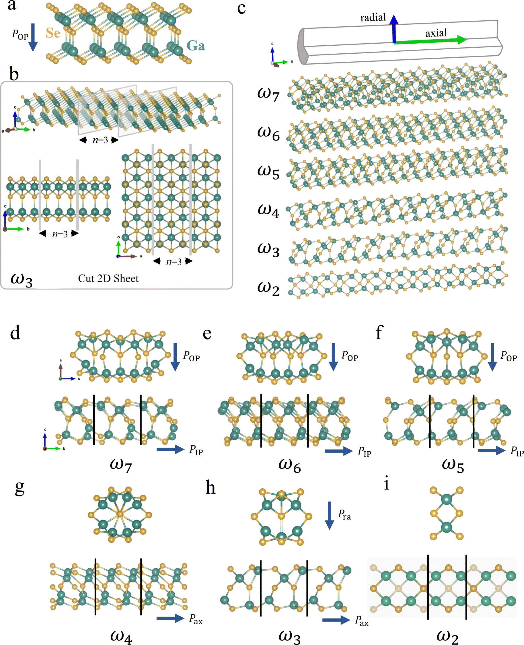 | ||
| Fig. 1 Structural evolution from 2D to 1D in α-Ga2Se3. (a) Structure of monolayer α-Ga2Se3 with out-of-plane polarization (POP). The Ga and Se atoms are represented by green and yellow balls, respectively. (b) Construction of the ω3 nanoribbon by cutting the 2D sheet with armchair-terminated edges. The cutting planes are colored in gray. (c) Schematic illustrating the axial direction (b-axis) and the radial direction (c-axis). The bottom illustrates optimized 1D nanostructures of Ga2Se3 from ω7 to ω2 with axial and side views shown from (d–i). The ω3 nanothread has both Pax and Pra. | ||
The 1D nanoribbons are constructed by cutting the α-III2VI3 monolayer with different edges and widths. Similar to graphene, the α-III2VI3 monolayer with a hexagonal lattice can be cut either along the zigzag direction or the armchair direction. We first explored the impact of edge terminations on the stability of nanoribbons for both α-In2Se3 and α-Ga2Se3. Our benchmark calculations showed that the zigzag edge is unstable due to the non-vanishing formal in-plane polarization and will undergo substantial atomic reconstruction that destroys the crystalline order. In contrast, the armchair edge is stable. In view of this, we focus on 1D nanoribbons with armchair-terminated edges. Following the convention, the width ωn is defined as the number (n) of armchair lines across the ribbon width (Fig. 1b).
The structural evolution of α-III2VI3 nanoribbons follows a similar trend with respect to the varying width. Here we use α-Ga2Se3 as an example. We find that with reducing n, the 1D Ga2Se3 changes gradually from a flat nanoribbon to a compact cylinder-like nanostructure, referred to as a nanothread (Fig. 1c). As shown in Fig. 1d–f, except for the notable relaxation of unsaturated edge atoms, ω7, ω6, and ω5 largely resemble the structure of monolayer α-Ga2Se3 and maintain the original POP. Specifically, the ω6 nanoribbon with a width of 13.34 Å exhibits POP of 0.48 eÅ originated from the displacement of the central Se layer; the magnitude of in-plane polarization (PIP) is also non-zero due to the breaking of the in-plane three-fold rotational symmetry after the cut. In the case of ω4, the 1D nanostructure becomes a nanothread characterized by a nearly circular base (Fig. 1g). The reconstruction of edge atoms completely suppresses Pra. Further reducing the width to ω3 surprisingly revives Pra: the ω3 nanothread (Fig. 1h) has both spontaneous Pra and Pax resulting from the displacement of the central Se atom relative to the center of the surrounding distorted Ga6 octahedron (see discussions below). Finally, ω2 can be viewed as an ultrathin nanoribbon with neighboring four-fold coordinated Se atoms displaced in an antiparallel manner (Fig. 1i), similar to an antiferroelectric.
Structural stability of ω3
Since the ω3 nanothread of III2VI3 is the smallest 1D system possessing both Pra and Pax, it is natural to ask how likely could such a 1D ferroelectric nanostructure be realized experimentally. A full resolution to this question with theory only is challenging. Nevertheless, we first estimate the structural stability of ω3 nanothreads by computing the phonon spectra following the general protocol of stability analysis for new materials designed computationally.55 A dynamically stable material is situated at a local minimum of the potential energy surface and will have all phonon frequencies being positive. A technical issue arises due to the 1D nature of the system: acoustic phonon modes tend to have rather low frequencies (close to zero) that make the accurate determination of the phonon spectrum quite difficult numerically. Using an extremely tight convergence threshold (10−16 Ry), we obtain the phonon spectra of all ω3 nanothreads of III2VI3 (see ESI†). It is found that ω3 of Ga2Se3 is dynamically stable as confirmed by a phonon spectrum without imaginary vibrational frequencies (Fig. 2b, left panel), while ω3 of Ga2S3, Ga2Te3, and Al2Te3 are marginally stable.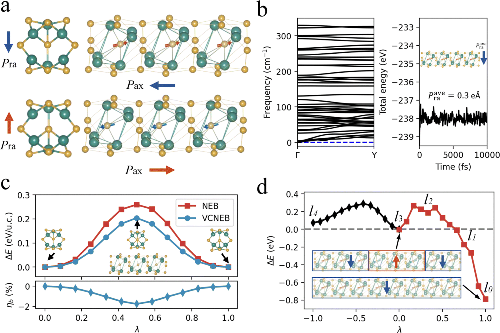 | ||
| Fig. 2 (a) Axial and side views of two energy-degenerate polar states with opposite polarization directions in the ω3 nanothread of Ga2Se3. The red arrow on the Se atom represents the local atomic displacement relative to the center of the Ga6 cage. (b) Phonon spectrum (left) and energy evolution as a function of time in AIMD at 200 K (right) for the ω3 nanothread of Ga2Se3. The inset shows the averaged structure using an equilibrium trajectory of 10 ps. (c) Minimum energy paths (MEPs) of polarization reversal identified with NEB (red) and VCNEB (blue). The bottom panel shows the variation of the lattice constant along the b axis during the switching process, ηb, defined as (b − b0)/b0. The insets show the axial and side views of the nonpolar structure. (d) MEPs of unit-cell-by-unit-cell switching obtained with NEB. The inset shows a l3 domain of upward Pra sandwiched by domains of downward Pra. | ||
Additionally, we perform AIMD simulations for the ω3 nanothread of Ga2Se3 using a 1 × 4 × 1 supercell to investigate its structural stability at finite temperatures (Fig. 2b, right panel). The averaged structure calculated using an equilibrium trajectory of 10 ps at 200 K remains almost the same as the structure optimized with the zero-Kelvin DFT method, and the magnitude of Pra is 0.3 eÅ per u.c., indicating a robust ferroelectricity at low temperatures. However, a higher temperature will drive structural amorphization. Further studies are needed to enhance the critical temperature for room-temperature applications. In the following, we will focus on the structural and electronic properties of the ω3 nanothread of Ga2Se3 for its dynamical stability as well as the fact that its 2D counterpart has been synthesized.48 It is noted that the approach of deriving 1D structures from 2D monolayers, as proposed here, could be extended to chemically analogous systems such as V2–VI3 monolayers.56–58
Ferroelectric switching in ω3 of Ga2Se3
The structural origin of the spontaneous polarization in ω3 of Ga2Se3 comes from the off-center displacement of the Se atom relative to the center of the surrounding Ga6 octahedron that is distorted along the bottom-left to top-right direction (Fig. 2a). Taking the configuration with the downward Pra for example, the central Se atom, locating almost vertically above a bottom Ga atom, forms three shorter bonds with top-right Ga atoms and three longer bonds with bottom-left Ga atoms, thus breaking the centrosymmetry and producing both Pra and Pax. Due to the rigidity of the Ga6 octahedron, the flip of Pra achieved via the movement of the central Se atom is inevitably accompanied by the reversal of Pax, a “dipole locking” mechanism similar to that in monolayer α-In2Se3.21 It is noted that the structural locking in α-In2Se3, though being beneficial for the stabilization of POP against the depolarization field, makes the switching of POP rather difficult: the whole central Se layer must move collectively and laterally to break and form multiple In-Se covalent bonds. In comparison, the dipole locking in ω3 of Ga2Se3 is confined within each individual Ga6 octahedron such that switching Pra and Pax only requires local Se movements within each unit cell, similar to the switching in perovskite ferroelectrics. This in principle will make the switching of 1DFENT easier and is a desirable feature to realize low-power ferroelectric-based devices. The magnitudes of Pax and Pra computed with the Berry phase approach are 0.32 eÅ and 2.84 eÅ per unit cell, respectively. Note that Pra of the ω3 nanothread of Ga2Se3 is even higher than POP of 0.094 eÅ per u.c. in monolayer α-In2Se3.20 Additionally, we compute the Born effective charge (BEC) tensors for Ga and Se atoms in both the ω3 nanothread and 2D monolayer. The BEC values for the ω3 nanothread of Ga2Se3, α-Ga2Se3 monolayer, α-In2Se3 monolayer, and bulk PbTiO3 are listed in Table 1. We find that there is a substantial correlation between the magnitude of BEC and dimensionality. Along the direction with reduced dimension, the value of BEC diminishes. For example, the values of and
and  are much smaller than those of
  in the ω3 nanothread; 2D monolayers possess low
  values.
| BEC | Ga2Se3-ω3 (1D) | α-Ga2Se3(2D) | α-In2Se3 (2D) | PbTiO3 (3D) | |||||
|---|---|---|---|---|---|---|---|---|---|
| Ga | Se | Ga | Se | In | Se | Pb | Ti | O | |

|
0.62 | 0.41 | 3.33 | 2.20 | 3.41 | 2.25 | 3.74 | 6.20 | 2.38 |

|
2.71 | 1.81 | 3.48 | 2.33 | 3.42 | 2.26 | 3.74 | 6.20 | 3.66 |

|
0.68 | 0.36 | 0.38 | 0.27 | 0.49 | 0.32 | 3.52 | 5.18 | 3.27 |
We further evaluate the polarization switchability by mapping out the MEP of polarization reversal using the NEB method in which the axial lattice constant of each image along the switching pathway is fixed to the ground-state value. The switching barrier obtained with NEB is 0.26 eV per u.c. (Fig. 2c), lower than the barrier of 0.33 eV per u.c. in tetragonal PbTiO3. This suggests that the polarization can be readily reserved by applying a radial external electric field. The MEP reveals that the polarization reversal process goes through a centrosymmetric nonpolar state that has the Se atom occupying the center of the Ga6 octahedron.
Previous studies have shown that the strain relaxation effect during the ferroelectric switching can impact the barrier height.61 We employ the VCNEB method to determine the MEP for the polarization reversal process that allows axial strain relaxation. The barrier estimated with VCNEB reduces to 0.2 eV per u.c. Interestingly, we observe an unusual variation in the axial strain ηb (defined as b/b0 − 1 with b0 the ground-state lattice constant) during the switching (Fig. 2c, bottom panel): the nanothread will first shrink along the axial direction and then expand until it recovers to b0 upon the completion of the reversal. This is distinct from the conventional ferroelectric switching process during which the transverse dimensions perpendicular to the polar axis will first expand and then recover (contract). The contraction of the axial dimension at the initial stage of the switching in the ω3 nanothread is a direct consequence of dipole locking as Pax (and thus ηb due to the polarization-strain coupling) must reduce together with Pra.
Minimum information storage unit in ω3 of Ga2Se3
One of the most exciting applications of ferroelectrics is for nonvolatile information storage. For a 3D bulk ferroelectric, one bit of information is often stored as a homogeneously polarized domain comprising thousands of atoms. The 1DFENT with radial polarization offers an opportunity to realize unit-cell-level data storage. To estimate the maximum theoretical data density, we first need to determine the critical length of a polar domain in ω3 of Ga2Se3. A potential issue is arises from the presence of axial polarization such that the 180° domain walls separating domains with opposite Pra will acquire positive (negative) bound charges due to Pax directed toward (from) the wall. We calculate energy barriers for unit-cell-by-unit-cell switching with NEB and identify a critical length of three unit cells (l3). As shown in Fig. 2d, the switching of one unit cell that changes a l4 domain to a l3 domain or vice versa needs to overcome a barrier of 0.28 eV, large enough to prevent spontaneous back-switching. However, smaller polar domains such as l2 and l1 are no longer stable, and they will spontaneously adopt the polar state of neighboring larger domains.We now give a rough estimation to the maximum theoretical data density enabled by 1DFENTs with radial polarization. We obtain the density of packed 1DFENTs by optimizing a cell containing four aligned ω3 nanothreads. The equilibrium distance between neighboring nanothreads is ≈3.5 Å. Assuming the l3 domain being the minimum storage unit, the theoretical data density for an atomically thin layer of 1DFENT array is ≈600 Gigabit mm−2 (see calculations in ESI†), 60 times higher than the current NAND areal density (≈10 Gigabit mm−2).62 Furthermore, by packing 1DFENTs into 3D arrays, the volumetric density could approach 600 Petabit mm−3. Note that these values are upper bounds since contacting electrodes are not considered.
Piezoelectric properties of ω3 of Ga2Se3
The dipole locking in the ω3 nanothread hints at unusual piezoelectricity. We compute the piezoelectric stress coefficients e32 and e22 from the slopes of polarization versus axial strain curves (Fig. 3) and find that both coefficients are of positive sign, an indication of the auxetic piezoelectric effect (APE) that stretching the nanothread will enhance both Pra and Pax. This is in sharp contrast with traditional piezoelectric materials in which the longitudinal and the transverse piezoelectric coefficients are of opposite signs. The auxetic piezoelectric effect can be viewed as a piezoelectric analogy of auxetic materials characterized by a negative Poisson's ratio.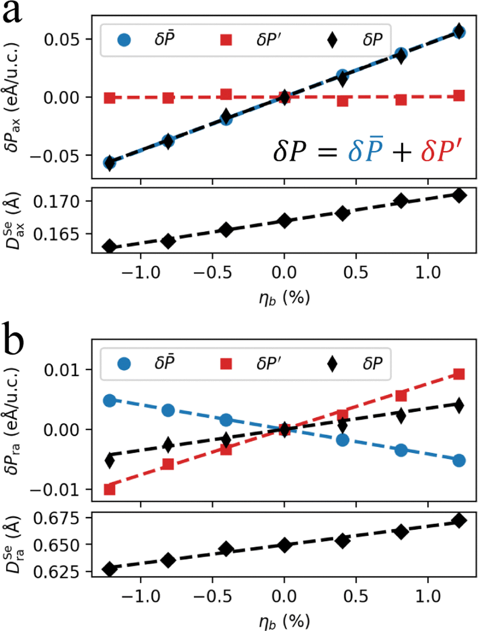 | ||
Fig. 3 Piezoelectricity of ω3 Ga2Se3. Variation of (a) axial polarization (δPax) and (b) radial polarization (δPra) and local displacements of Se atoms (DSe) as a function of axial strain (ηb). The change in polarization is decomposed into the clamped-ion contribution (δ![[P with combining macron]](https://www.rsc.org/images/entities/i_char_0050_0304.gif) ) and internal-strain contribution (δP′). ) and internal-strain contribution (δP′). | ||
To understand the origin of APE, we decompose the axial strain-induced polarization change (δP) into the clamped-ion contribution (δ) computed with the internal atomic coordinates fixed at their zero-strain values and the internal-strain contribution (δP′) arising from ion relaxations, δP = δ + δP′. Similar decomposition can be made to the total piezoelectric coefficient,  , using eij = ∂Pi/ηj.63,64 We find that for the axial polarization, the clamped-ion term makes the dominate contribution (δPax ≈ δax) while the internal-strain contribution is close to zero, indicating that the electronic relaxation is responsible for the axial piezoelectric response e22. Interestingly, for the radial polarization, δra is negative due to a tensile axial strain (ηb > 0), leading to a negative clamped-ion ē32. The total positive response of e32 > 0 results from the positive internal-strain contribution of
  . Structurally, the APE is a manifestation of dipole locking: the tensile axial strain will promote the Se displacement along the axis (DSeax) as well as the “locked” radial displacement (DSera), thus enhancing both Pra and Pax.
Electronic properties of ω3 of Ga2Se3
The PBEsol band structure of ω3 of Ga2Se3 is presented in Fig. 4a, revealing a direct band gap of 1.5 eV at Y. The projected density of states (PDOS) shows that the valence band maximum (VBM) takes almost exclusively a Se-4p character while the conduction band minimum (CBM) consists of Se-4p and Ga-4p characters. Most bands have small bandwidths. For example, the bandwidth of the highest valence band is only 0.18 eV, indicating that the contributing Se-4p orbitals are mostly localized with weak inter-orbital hybridizations.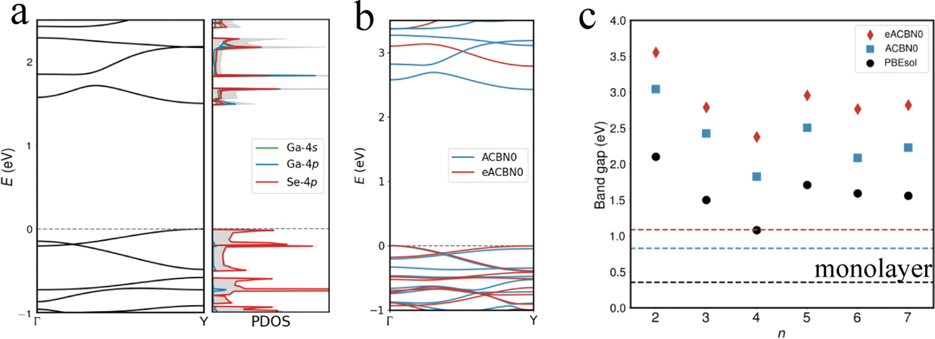 | ||
| Fig. 4 Electronic structure of ω3 Ga2Se3. (a) Band structure and projected density of states computed with PBEsol. (b) Band structures computed with ACBN0 and eACBN0. (c) Band gap as a function of width n of the 1D nanostructure of Ga2Se3. | ||
Since the semi-local density functionals like PBEsol often underestimate the band gap, we further compute the band structure using the newly developed pseudohybrid Hubbard density functional, Agapito–Cuetarolo–Buongiorno Nardelli (ACBN0)65 and the extended version (eACBN0).66,67 The ACBN0 function is essentially a DFT+U method with Hubbard parameter U computed self-consistently. The eACBN0, a DFT+U+V method, takes into account the intersite Coulomb interaction V between neighboring Hubbard sites. Previous studies have demonstrated that for a wide range of materials, ACBN0 and eACBN0 have improved accuracy over PBE and are on par with advanced methods such as the Heyd–Scuseria–Ernzerhof (HSE) hybrid density functional and GW approximations but at a lower cost.38,59,66,68,69 Particularly for low-dimensional materials, the reliability of HSE that assumes a fixed dielectric screening is not justified.70 The inclusion of self-consistent Hubbard parameters helps to capture the rapid variation in Coulomb screening in low dimensions. The ACBN0 and eACBN0 band structures of the ω3 nanothread of Ga2Se3 are presented in Fig. 4b, and the predicted band gaps are 2.47 and 2.79 eV, respectively. We further calculate the band gaps for all 1D nanostructures of Ga2Se3 discussed in Fig. 1. The eACBN0 method consistently predicts a larger band gap than ACBN0, followed by PBEsol, and all nanostructures have larger band gaps than monolayer α-Ga2Se3 (0.35 eV for PBEsol, 0.83 eV for ACBN0, and 1.09 eV for eACBN0, respectively). We notice that flat nanoribbons such as ω7, ω6, and ω5 possess an oscillation relationship between the band gap and ribbon width. The same trend has also been reported in BSb nanoribbons.71
Coexistence of 1D ferroelectricity and ferromagnetism in ω3
The narrow electronic bands in w3 of Ga2Se3 lead to high values of density of states. According to the Stoner criterion, it is possible to induce Stoner-type magnetism by adjusting the Fermi level (EF) to the energy level associated with a high density of states via appropriate charge doping.72,73 If the charge doping does not destroy the long-range polar ordering, the doped 1D system could host both ferroelectricity and ferromagnetism.We examine the ferroelectric and magnetic properties of ω3 as a function of charge-carrier concentration (Q in the unit of electron/hole per unit cell) at the PBEsol level. As shown in Fig. 5a, our results reveal the emergence of a spontaneous time-reversal symmetry breaking in both electron-doped and hole-doped ω3 over a wide range of doping concentrations from Q = −0.5 to 0.5 e per u.c. The doping-induced ferromagnetism is further confirmed by calculating the spin polarization energy defined as the energy difference between the nonmagnetic (NM) state and the ferromagnetic (FM) state, E(NM) − E(FM). We find that the spin polarization energy remains positive at all studied doping concentrations and increases with increasing magnitude of Q, indicating a strong magnetic instability at the nonmagnetic state that drives the spontaneous breaking of the time-reversal symmetry. The value of averaged magnetic moment per carrier (μ) has a constant value of 1 independent of Q. This shows that all doped carriers are spin polarized.
 | ||
| Fig. 5 Ferromagnetism of charge-doped ω3 Ga2Se3. (a) Spin polarization energy E(NM) − E(FM), radial polarization, and magnetic moment (μ in Bohr magneton μB per carrier) as a function of doping concentration (Q). (b) Doping-induced change in the radial polarization (δPra) and lattice constant b as a function of Q. δPra is decomposed into charge-carrier contribution (δPqra), ion relaxation contribution (δPira), and strain contribution (δPηra). Spin-polarized band structures for (c) electron and (d) hole doping. The insets show the spin-polarized charge density isosurfaces. | ||
In bulk ferroelectrics, the metallicity and ferroelectricity are often mutually exclusive since charge carriers will screen long-range Coulomb interactions that drive the structural distortion.74 An important question here is whether the long-range polar ordering in the w3 nanothread could survive the charge doping. Unexpectedly, as shown in Fig. 5b, both electron and hole doping will enhance the magnitude of Pra. Following a similar protocol in ref. 55 and 56, we perform three calculations in order to identify and separate contributions to the charge-carrier-induced change in Pra relative to the undoped value. Starting with the undoped nanothread, we first compute the change in Pra after introducing charge carriers with atomic positions and lattice constants fixed; we refer to this polarization change as the charge-carrier contribution, δPqra. Then we relax the atomic positions with fixed lattice constant b; the further induced polarization change is called the ion relaxation contribution, δPira. Finally, the lattice constant b and the atomic positions are fully relaxed; we name this third component as strain contribution, δPηra. Therefore, the total change in polarization is decomposed as δPra = δPqra + δPira + δPηra. The Q-dependence of δPqra follows the conventional understanding that charge carriers will suppress the polarization: both hole and electron doping give negative values of δPqra. In contrast, the ion-relaxation contribution promotes Pra as all values of δPira are positive. The strain contribution follows the APE discussed above: the electron doping increases b, thus leading to positive δPηra whereas the hole doping reduces b and causes negative δPηra. Overall, the polarization enhancement along the radial direction is because of both ion relaxation and strain contributions in the electron doped region but solely due to the ion relaxation in the hole doped region.
Charge doping induced electronic transition
The evolution of the spin-polarized band structures as a function of the concentration of doped electrons reveals a doping-driven band flattening: the bandwidth (t) of the spin-up and spin-down bands near the EF reduces from 160 meV at Q = −0.3 to 45 meV at Q = −1.0 (Fig. 5c). Meanwhile, the energy difference between the two bands, roughly viewed as the strength of on-site Coulomb repulsion (U), increases from 2.95 eV to 3.14 eV (for Se-4p orbitals). The electron-doped ω3 of Ga2Se3 is a charge-carrier-mediated ferromagnetic metal before reaching the critical concentration of Q = −1 at which the system becomes a fully gaped insulator. Different from the band insulator at Q = 0, the Q = −1 system can be viewed as a 1D two-level system at half filling with U/t ≫ 1 and is an interaction-induced insulator in which each unit cell hosts a localized doped electron, resembling the Hund's rule for orbital filling. Because of the small t, the exchange coupling between neighboring spins is expected to be weak. Consequently, the antiferromagnetic state will have energy comparable with the ferromagnetic state at 0 K. This is confirmed with DFT calculations that show that the antiferromagnetic state is slightly higher in energy by 0.7 meV per unit cell than the ferromagnetic state. At an elevated temperature, the ω3 nanothread at Q = −1 is most likely a paramagnetic state due to the weak exchange interaction.In comparison, the hole doping impacts the band dispersion to a lesser degree, but enhances the exchange splitting between the spin-up and spin-down bands. Moreover, we find that the hole-doped ω3 is a ferromagnetic metal protected by the mirror reflection symmetry with respect to the xy plane  . The highest two valence bands exhibit opposite
  parities as marked by +1 and −1 in Fig. 5d. The crossing point (labeled as γ) between the two bands belonging to different irreducible representations is symmetry protected and will not hybridize to open a gap regardless of the hole doping concentration. Consequently, the hole-doped ω3 is a symmetry-protected ferromagnetic metal.
Conclusions
In summary, we predict a 1D ferroelectric nanothread of ultrasmall diameter that exhibits both axial and radial polarization based on first-principles density functional theory calculations. We show that there is a spontaneous structural evolution from nanoribbon to nanothread with reducing nanoribbon width. The switchable radial polarization afforded by the ω3 nanothread of Ga2Se3 has the potential to realize ultimately-dense ferroelectric-based electronic devices in which a 1D domain of just three unit cells could serve as the functional unit. The dipole locking feature gives rise to an intriguing 1D auxetic piezoelectric effect that the axial stretching promotes both radial and axial polarization. Moreover, the 1D ferroelectricity is robust against both electron and hole doping, enabling the coexistence of ferroelectricity, ferromagnetism, and metallicity. The intrinsic flatness of the electronic bands in the 1D nanothread offers a platform to explore exotic states of matter such as Hund's insulator-like semiconductor. Our DFT calculations offer theoretical evidence supporting the structural stability of the proposed 1D ferroelectric nanothreads. We hope that the proof-of-concept reported in this work will motivate experimental studies toward the synthesis of this new family of low-dimensional ferroelectrics.Data availability
The data that support the findings of this study are included in this article and are available from the corresponding author upon reasonable request.Author contributions
J. H. conceived the design principle. J. H. and C. K. performed calculations and data analysis. S. L. supervised the project. All authors contributed to the discussion and the manuscript preparation.Conflicts of interest
The authors declare no competing financial or non-financial interests.Acknowledgements
J. H., C. K., and S. L. acknowledge the support from Westlake Education Foundation, and Westlake Multidisciplinary Research Initiative Center, and National Natural Science Foundation of China (52002335). The computational resource was provided by the Westlake HPC Center.References
- E. Ising, Beitrag zur Theorie des Ferromagnetismus, Z. Physik, 1925, 31, 253–258 CrossRef CAS.
- N. D. Mermin and H. Wagner, Absence of Ferromagnetism or Antiferromagnetism in One- or Two-Dimensional Isotropic Heisenberg Models, Phys. Rev. Lett., 1966, 17, 1133–1136 CrossRef CAS.
- F. J. Dyson, Existence of a phase-transition in a one-dimensional Ising ferromagnet, Commun. Math. Phys., 1969, 12, 91–107 CrossRef.
- M. Takahashi and M. Suzuki, One-Dimensional Anisotropic Heisenberg Model at Finite Temperatures, Prog. Theor. Phys., 1972, 48, 2187–2209 CrossRef.
- J. Linares, H. Spiering and F. Varret, Analytical solution of 1D Ising-like systems modified by weak long range interaction, Eur. Phys. J. B, 1999, 10, 271–275 CrossRef CAS.
- M. F. Maghrebi, Z.-X. Gong and A. V. Gorshkov, Continuous Symmetry Breaking in 1D Long-Range Interacting Quantum Systems, Phys. Rev. Lett., 2017, 119, 023001 CrossRef PubMed.
- B. Huang, G. Clark, E. Navarro-Moratalla, D. R. Klein, R. Cheng, K. L. Seyler, D. Zhong, E. Schmidgall, M. A. McGuire, D. H. Cobden, W. Yao, D. Xiao, P. Jarillo-Herrero and X. Xu, Layer-dependent ferromagnetism in a van der Waals crystal down to the monolayer limit, Nature, 2017, 546, 270–273 CrossRef CAS PubMed.
- C. Gong, L. Li, Z. Li, H. Ji, A. Stern, Y. Xia, T. Cao, W. Bao, C. Wang, Y. Wang, Z. Q. Qiu, R. J. Cava, S. G. Louie, J. Xia and X. Zhang, Discovery of intrinsic ferromagnetism in two-dimensional van der Waals crystals, Nature, 2017, 546, 265–269 CrossRef CAS PubMed.
- Y. Deng, Y. Yu, Y. Song, J. Zhang, N. Wang, Z. Sun, Y. Yi, Y. Z. Wu, S. Wu, J. Zhu, J. S. Wang, X. H. Chen and Y. Zhang, Gate-tunable room-temperature ferromagnetism in two-dimensional Fe3GeTe2, Nature, 2018, 563, 94–99 CrossRef CAS PubMed.
- Z. Wu, Z. Shen, Y. Xue and C. Song, Strain-induced topological phase transition and enhanced Curie temperature in MnBi2Te4/CrI3 heterojunction, Phys. Rev. Mater., 2022, 6, 014011 CrossRef CAS.
- J. M. Law, P. Reuvekamp, R. Glaum, C. Lee, J. K. Kang, M.-H. Whangbo and R. K. Kremer, Quasi-one-dimensional antiferromagnetism and multiferroicity in CuCrO4, Phys. Rev. B: Condens. Matter Mater. Phys., 2011, 84, 014426 CrossRef.
- R. Fei, W. Kang and L. Yang, Ferroelectricity and Phase Transitions in Monolayer Group-IV Monochalcogenides, Phys. Rev. Lett., 2016, 117, 097601 CrossRef PubMed.
- K. Chang, J. Liu, H. Lin, N. Wang, K. Zhao, A. Zhang, F. Jin, Y. Zhong, X. Hu and W. Duan, et al., Discovery of robust in-plane ferroelectricity in atomic-thick SnTe, Science, 2016, 353, 274–278 CrossRef CAS PubMed.
- S. Yuan, X. Luo, H. L. Chan, C. Xiao, Y. Dai, M. Xie and J. Hao, Room-temperature ferroelectricity in MoTe2 down to the atomic monolayer limit, Nat. Commun., 2019, 10, 1175 CrossRef PubMed.
- Q. Yang, M. Wu and J. Li, Origin of two-dimensional vertical ferroelectricity in WTe2 bilayer and multilayer, J. Phys. Chem. Lett., 2018, 9, 7160–7164 CrossRef CAS PubMed.
- C. Yang, M. Chen, S. Li, X. Zhang, C. Hua, H. Bai, C. Xiao, S. A. Yang, P. He, Z. an Xu and Y. Lu, Coexistence of Ferroelectricity and Ferromagnetism in One-Dimensional SbN and BiN Nanowires, ACS Appl. Mater. Interfaces, 2021, 13, 13517–13523 CrossRef CAS PubMed.
- J. Junquera and P. Ghosez, Critical thickness for ferroelectricity in perovskite ultrathin films, Nature, 2003, 422, 506–509 CrossRef CAS PubMed.
- F. Liu, et al., Room-temperature ferroelectricity in CuInP2S6 ultrathin flakes, Nat. Commun., 2016, 7, 12357 CrossRef CAS PubMed.
- Y. Zhou, D. Wu, Y. Zhu, Y. Cho, Q. He, X. Yang, K. Herrera, Z. Chu, Y. Han, M. C. Downer, H. Peng and K. Lai, Out-of-Plane Piezoelectricity and Ferroelectricity in Layered α-In2Se3 Nanoflakes, Nano Lett., 2017, 17, 5508–5513 CrossRef CAS PubMed.
- W. Ding, J. Zhu, Z. Wang, Y. Gao, D. Xiao, Y. Gu, Z. Zhang and W. Zhu, Prediction of intrinsic two-dimensional ferroelectrics in In2Se3 and other III2 -VI3 van der Waals materials, Nat. Commun., 2017, 8, 14956 CrossRef CAS PubMed.
- J. Xiao, H. Zhu, Y. Wang, W. Feng, Y. Hu, A. Dasgupta, Y. Han, Y. Wang, D. A. Muller, L. W. Martin, P. Hu and X. Zhang, Intrinsic Two-Dimensional Ferroelectricity with Dipole Locking, Phys. Rev. Lett., 2018, 120, 227601 CrossRef CAS PubMed.
- S. Wan, Y. Li, W. Li, X. Mao, W. Zhu and H. Zeng, Room-temperature ferroelectricity and a switchable diode effect in two-dimensional α-In2Se3 thin layers, Nanoscale, 2018, 10, 14885–14892 RSC.
- S. Wan, Y. Li, W. Li, X. Mao, C. Wang, C. Chen, J. Dong, A. Nie, J. Xiang, Z. Liu, W. Zhu and H. Zeng, Nonvolatile Ferroelectric Memory Effect in Ultrathin α-In2 Se3, Adv. Funct. Mater., 2019, 29, 1808606 CrossRef.
- J. E. Spanier, A. M. Kolpak, J. J. Urban, I. Grinberg, L. Ouyang, W. S. Yun, A. M. Rappe and H. Park, Ferroelectric Phase Transition in Individual Single-Crystalline BaTiO3 Nanowires, Nano Lett., 2006, 6, 735–739 CrossRef CAS PubMed.
- G. Geneste, E. Bousquet, J. Junquera and P. Ghosez, Finite-size effects in BaTiO3 nanowires, Appl. Phys. Lett., 2006, 88, 112906 CrossRef.
- J. Hong and D. Fang, Systematic study of the ferroelectric properties of Pb(Zr0.5Ti0.5)O3 nanowires, J. Appl. Phys., 2008, 104, 064118 CrossRef.
- L. Louis, P. Gemeiner, I. Ponomareva, L. Bellaiche, G. Geneste, W. Ma, N. Setter and B. Dkhil, Low-Symmetry Phases in Ferroelectric Nanowires, Nano Lett., 2010, 10, 1177–1183 CrossRef CAS PubMed.
- L. Zhang, C. Tang, S. Sanvito and A. Du, Purely one-dimensional ferroelectricity and antiferroelectricity from van der Waals niobium oxide trihalides, npj Comput. Mater., 2021, 7, 135 CrossRef CAS.
- J.-J. Zhang, J. Guan, S. Dong and B. I. Yakobson, Room-Temperature Ferroelectricity in Group-IV Metal Chalcogenide Nanowires, J. Am. Chem. Soc., 2019, 141, 15040–15045 CrossRef CAS PubMed.
- L.-F. Lin, Y. Zhang, A. Moreo, E. Dagotto and S. Dong, Quasi-one-dimensional ferroelectricity and piezoelectricity in WOX4 halogens, Phys. Rev. Mater., 2019, 3, 111401(R) CrossRef.
- B. Chen, R. Hoffmann, N. Ashcroft, J. Badding, E. Xu and V. Crespi, Linearly polymerized benzene arrays as intermediates, tracing pathways to carbon nanothreads, J. Am. Chem. Soc., 2015, 137, 14373–14386 CrossRef CAS PubMed.
- T. C. Fitzgibbons, M. Guthrie, E.-S. Xu, V. H. Crespi, S. K. Davidowski, G. D. Cody, N. Alem and J. V. Badding, Benzene-derived carbon nanothreads, Nat. Mater., 2015, 14, 43–47 CrossRef CAS PubMed.
- E.-s Xu, P. E. Lammert and V. H. Crespi, Systematic enumeration of sp3 nanothreads, Nano Lett., 2015, 15, 5124–5130 CrossRef CAS PubMed.
- P. Giannozzi, S. Baroni, N. Bonini, M. Calandra, R. Car, C. Cavazzoni, D. Ceresoli, G. L. Chiarotti, M. Cococcioni and I. Dabo, et al., QUANTUM ESPRESSO: a modular and open-source software project for quantum simulations of materials, J. Phys.: Condens. Matter, 2009, 21, 395502 CrossRef PubMed.
- P. Giannozzi, O. Andreussi, T. Brumme, O. Bunau, M. B. Nardelli, M. Calandra, R. Car, C. Cavazzoni, D. Ceresoli and M. Cococcioni, et al., Advanced capabilities for materials modelling with QUANTUM ESPRESSO, J. Phys.: Condens. Matter, 2017, 29, 465901 CrossRef CAS PubMed.
- K. F. Garrity, J. W. Bennett, K. M. Rabe and D. Vanderbilt, Pseudopotentials for High-Throughput DFT Calculations, Comput. Mater. Sci., 2014, 81, 446–452 CrossRef CAS.
- L. Bengtsson, Dipole correction for surface supercell calculations, Phys. Rev. B: Condens. Matter Mater. Phys., 1999, 59, 12301–12304 CrossRef CAS.
- X. Duan, J. Huang, B. Xu and S. Liu, A two-dimensional multiferroic metal with voltage-tunable magnetization and metallicity, Mater. Horiz., 2021, 8, 2316–2324 RSC.
- M. Kawamura, Y. Gohda and S. Tsuneyuki, Improved tetrahedron method for the Brillouin-zone integration applicable to response functions, Phys. Rev. B: Condens. Matter Mater. Phys., 2014, 89, 094515 CrossRef.
- S. Baroni, P. Giannozzi and A. Testa, Green's-function approach to linear response in solids, Phys. Rev. Lett., 1987, 58, 1861–1864 CrossRef CAS PubMed.
- X. Gonze, Perturbation expansion of variational principles at arbitrary order, Phys. Rev. A, 1995, 52, 1086–1095 CrossRef PubMed.
- G. Kresse and J. Furthmüller, Efficient iterative schemes for ab initio total-energy calculations using a plane-wave basis set, Phys. Rev. B: Condens. Matter Mater. Phys., 1996, 54, 11169–11186 CrossRef CAS PubMed.
- G. Kresse and J. Furthmüller, Efficiency of ab-initio total energy calculations for metals and semiconductors using a plane-wave basis set, Comput. Mater. Sci., 1996, 6, 15–50 CrossRef CAS.
- A. R. Oganov and C. W. Glass, Crystal Structure Prediction Using Ab Initio Evolutionary Techniques: Principles and Applications, J. Chem. Phys., 2006, 124, 244704 CrossRef PubMed.
- A. O. Lyakhov, A. R. Oganov, H. T. Stokes and Q. Zhu, New Developments in Evolutionary Structure Prediction Algorithm USPEX, Comput. Phys. Commun., 2013, 184, 1172–1182 CrossRef CAS.
- A. R. Oganov, A. O. Lyakhov and M. Valle, How Evolutionary Crystal Structure Prediction Works—and Why, Acc. Chem. Res., 2011, 44, 227–237 CrossRef CAS PubMed.
- Jiawei Huang, 1DFENT supplementary materials: inputs and outputs. 2022, https://zenodo.org/record/7394651.
- W. Xue, Q. Jiang, F. Wang, R. He, R. Pang, H. Yang, P. Wang, R. Yang, Z. Zhong, T. Zhai and X. Xu, Discovery of Robust Ferroelectricity in 2D Defective Semiconductor α-Ga2Se3, Small, 2022, 18, 2105599 CrossRef CAS PubMed.
- R. D. King-Smith and D. Vanderbilt, Theory of polarization of crystalline solids, Phys. Rev. B: Condens. Matter Mater. Phys., 1993, 47, 1651–1654 CrossRef CAS PubMed.
- R. Resta, Macroscopic Electric Polarization as a Geometric Quantum Phase, Europhys. Lett., 1993, 22, 133–138 CrossRef CAS.
- D. Vanderbilt and R. D. King-Smith, Electric polarization as a bulk quantity and its relation to surface charge, Phys. Rev. B: Condens. Matter Mater. Phys., 1993, 48, 4442–4455 CrossRef CAS PubMed.
- M. Gibertini and N. Marzari, Emergence of One-Dimensional Wires of Free Carriers in Transition-Metal-Dichalcogenide Nanostructures, Nano Lett., 2015, 15, 6229–6238 CrossRef CAS PubMed.
- M. Kruse, U. Petralanda, M. N. Gjerding, K. W. Jacobsen, K. S. Thygesen and T. Olsen, Two-dimensional ferroelectrics from high throughput computational screening, arXiv, 2022, preprint, arXiv:2102.11508.
- Z. Qiao, S. A. Yang, B. Wang, Y. Yao and Q. Niu, Spin-polarized and valley helical edge modes in graphene nanoribbons, Phys. Rev. B: Condens. Matter Mater. Phys., 2011, 84, 035431 CrossRef.
- H. Peelaers, B. Partoens and F. Peeters, Phonon band structure of Si nanowires: a stability analysis, Nano Lett., 2009, 9, 107–111 CrossRef CAS PubMed.
- B. Mortazavi, F. Shojaei, M. Azizi, T. Rabczuk and X. Zhuang, As2S3, As2Se3 and As2Te3 nanosheets: superstretchable semiconductors with anisotropic carrier mobilities and optical properties, J. Mater. Chem. C, 2020, 8, 2400–2410 RSC.
- Y. Z. Abdullahi, R. Caglayan, A. Mogulkoc, Y. Mogulkoc and F. Ersan, New stable ultrawide bandgap As2O3 semiconductor materials, J. Phys. Mater., 2023, 6, 025003 CrossRef.
- J. Lee, Y. I. Jhon, K. Lee, Y. M. Jhon and J. H. Lee, Nonlinear optical properties of arsenic telluride and its use in ultrafast fiber lasers, Sci. Rep., 2020, 10, 15305 CrossRef CAS PubMed.
- C. Ke, J. Huang and S. Liu, Two-dimensional ferroelectric metal for electrocatalysis, Mater. Horiz., 2021, 8, 3387–3393 RSC.
- G. Sághi-Szabó, R. E. Cohen and H. Krakauer, First-Principles Study of Piezoelectricity in PbTiO3, Phys. Rev. Lett., 1998, 80, 4321–4324 CrossRef.
- J. Huang, Y. Hu and S. Liu, Origin of ferroelectricity in magnesium-doped zinc oxide, Phys. Rev. B, 2022, 106, 144106 CrossRef CAS.
- J.-W. Park et al. 30.1 A 176-Stacked 512Gb 3b/Cell 3D-NAND Flash with 10.8Gb/mm2 Density with a Peripheral Circuit Under Cell Array Architecture. 2021 IEEE International Solid-State Circuits Conference (ISSCC). 2021.
- G. Sághi-Szabó, R. E. Cohen and H. Krakauer, First-Principles Study of Piezoelectricity in PbTiO3, Phys. Rev. Lett., 1998, 80, 4321–4324 CrossRef.
- S. Liu and R. E. Cohen, Origin of Negative Longitudinal Piezoelectric Effect, Phys. Rev. Lett., 2017, 119, 207601 CrossRef PubMed.
- L. A. Agapito, A. Ferretti, A. Calzolari, S. Curtarolo and M. B. Nardelli, Effective and accurate representation of extended Bloch states on finite Hilbert spaces, Phys. Rev. B: Condens. Matter Mater. Phys., 2013, 88, 165127 CrossRef.
- S.-H. Lee and Y.-W. Son, First-principles approach with a pseudohybrid density functional for extended Hubbard interactions, Phys. Rev. Research, 2020, 2, 043410 CrossRef CAS.
- N. Tancogne-Dejean and A. Rubio, Parameter-free hybridlike functional based on an extended Hubbard model: DFT+U+V, Phys. Rev. B, 2020, 102, 155117 CrossRef CAS.
- J. Huang, S.-H. Lee, Y.-W. Son, A. Supka and S. Liu, First-principles study of two-dimensional ferroelectrics using self-consistent Hubbard parameters, Phys. Rev. B, 2020, 102, 165157 CrossRef CAS.
- J. Yang, T. Zhu and S. Liu, Onsite and intersite electronic correlations in the Hubbard model for halide perovskites, Phys. Rev. B, 2022, 106, 195159 CrossRef CAS.
- M. Jain, J. R. Chelikowsky and S. G. Louie, Reliability of Hybrid Functionals in Predicting Band Gaps, Phys. Rev. Lett., 2011, 107, 216806 CrossRef PubMed.
- F. Ersan, G. Gökoğlu and E. Aktürk, Electronic structure of BSb defective monolayers and nanoribbons, J. Phys.: Condens. Matter, 2014, 26, 325303 CrossRef CAS PubMed.
- T. Cao, Z. Li and S. G. Louie, Tunable Magnetism and Half-Metallicity in Hole-Doped Monolayer GaSe, Phys. Rev. Lett., 2015, 114, 236602 CrossRef PubMed.
- L. Seixas, A. S. Rodin, A. Carvalho and A. H. Castro Neto, Multiferroic Two-Dimensional Materials, Phys. Rev. Lett., 2016, 116, 206803 CrossRef CAS PubMed.
- Y. Wang, X. Liu, J. D. Burton, S. S. Jaswal and E. Y. Tsymbal, Ferroelectric Instability Under Screened Coulomb Interactions, Phys. Rev. Lett., 2012, 109, 247601 CrossRef PubMed.
Footnote |
| † Electronic supplementary information (ESI) available: Phonon spectra of ω3 nanothreads of III2VI3 (Section I), and packed ω3 nanothreads (Secttion II). See DOI: https://doi.org/10.1039/d3nh00154g |
| This journal is © The Royal Society of Chemistry 2023 |