
Depolarization induced III–V triatomic layers with tristable polarization states†
Changming
Ke
 ab,
Yihao
Hu
ab and
Shi
Liu
*ab
ab,
Yihao
Hu
ab and
Shi
Liu
*ab
aKey Laboratory for Quantum Materials of Zhejiang Province, Department of Physics, School of Science, Westlake University, Hangzhou, Zhejiang 310030, China. E-mail: liushi@westlake.edu.cn
bInstitute of Natural Sciences, Westlake Institute for Advanced Study, Hangzhou, Zhejiang 310024, China
First published on 10th March 2023
Abstract
The integration of ferroelectrics that exhibit high dielectric, piezoelectric, and thermal compatibility with the mainstream semiconductor industry will enable novel device types for widespread applications, and yet there are few silicon-compatible ferroelectrics suitable for device downscaling. We demonstrate with first-principles calculations that the enhanced depolarization field at the nanoscale can be utilized to soften unswitchable wurtzite III–V semiconductors, resulting in ultrathin two-dimensional (2D) sheets possessing reversible polarization states. A 2D sheet of AlSb consisting of three atomic planes is identified to host both ferroelectricity and antiferroelectricity, and the tristate switching is accompanied by a metal–semiconductor transition. The thermodynamic stability and potential synthesizability of the triatomic layer are corroborated with phonon spectrum calculations, ab initio molecular dynamics simulations, and variable-composition evolutionary structure search. We propose a 2D AlSb-based homojunction field effect transistor that supports three distinct and nonvolatile resistance states. This new class of III–V semiconductor-derived 2D materials with dual ferroelectricity and antiferroelectricity opens up the opportunity for nonvolatile multibit-based integrated nanoelectronics.
New conceptsThe strong coupling between polarization, strain, and electronic degrees of freedom of ferroelectrics has made them critical components in numerous devices, but it remains challenging to integrate ferroelectrics with the mainstream semiconductor industry as few ferroelectrics are silicon compatible. Here, the depolarization field that is often considered detrimental to ferroelectric properties is employed as a physical stressor to soften unswitchable III–V wurtzite piezoelectrics, creating switchable two-dimensional (2D) polar materials with promising silicon compatibility. Moreover, the delicate competition between different energy terms at the nanoscale and under open-circuit boundary conditions leads to a new class of 2D materials with dual ferroelectricity and antiferroelectricity, opening the possibility for nonvolatile multibit-based integrated nanoelectronics. |
Ferroelectricity, as an extensively studied dipolar ordering state of insulators, is characterized by electrically switchable polarization. The strong coupling between polarization, strain, and electronic degrees of freedom of ferroelectrics has made them critical components in numerous devices such as sensors, actuators, and nonvolatile memories.1,2 The continuing demand for miniaturized electronics has imposed stringent requirements on ferroelectrics. In particular, to incorporate ferroelectric functionalities into integrated circuits via the current semiconductor manufacturing process, materials with nanoscale switchable dipoles and silicon compatibility are essential.3
Two-dimensional (2D) ferroelectrics with long-range dipolar ordering in atom-thick crystalline layers are promising materials for ferroelectric-based nanoelectronics because of their various merits such as the uniform atomic thickness for high-density integration and the easy preparation of high-quality interface in van der Waals heterostructures.4 However, similar to perovskite ferroelectrics, most 2D ferroelectrics also suffer from the depolarization effect such that they often have the polarization developed in-plane,5,6 a feature that is inconvenient for lateral downscaling. Atomically thin monolayers with out-of-plane polarization (POP) are rare, and few notable examples confirmed experimentally are CuInP2S6,7 α-In2Se3,8–13 MoTe2,14 and WTe2.15 Additionally, it remains unclear how to integrate these 2D ferroelectrics with the mainstream semiconductor technology.
A strategy to obtain new ferroelectrics suitable for integrated systems is to “soften” silicon-compatible piezoelectrics to make them switchable by applying appropriate “stressors”.16 For example, by substituting Sc into a well-known nitride piezoelectric, AlN, Fichtner et al. realized a giant switchable polarization (80–110 μC cm−2) in Al1−xScxN.17 More recently, starting with another widely used piezoelectric, ZnO, Ferri et al. synthesized thin films of Zn1−xMgxO and reported even larger switchable polarization of >100 μC cm−2 and coercive fields below 3 MV cm−1 at room temperature.16 In both cases, the essence is to destabilize an unswitchable piezoelectric by applying a chemical stressor.
We propose to “physically soften” silicon-compatible piezoelectrics represented by III–V wurtzite piezoelectrics via dimension reduction. Products based on III–V semiconductors have been widely employed in mobile devices, wireless networks, satellite communications, and optoelectronics.18–20 For example, 4th-generation (4G) wireless networks depend on thin-film bulk acoustic resonators consisting of piezoelectric wurtzite AlN. At present, the industry of III–V semiconductor manufacturing is well established. Several approaches such as direct growth of III–V on Si, III–V on lattice engineered substrates, and III–V on Ge–Si templates have been developed to integrate III–V compounds with the cutting-edge modern complementary metal oxide semiconductor (CMOS) technology.21,22 Therefore, III–V semiconductor-based 2D ferroelectrics, if available, will reduce the barrier of integrating ferroelectric functionalities with silicon-based technology and lower the cost of commercialization.
The physical stressor we employ is the enhanced depolarization field at the nanoscale. The depolarization field (Ed) arising from the incomplete screening of surface polarization bound charges scales inversely with the film thickness (Ed ∝ Ps/d with Ps being the remnant polarization and d the film thickness).23 In thin films of conventional perovskite ferroelectrics such as PbTiO3, the intrinsic double-well energy landscape of a ferroelectric will eventually be flattened out by the pronounced depolarization field in thin films below a critical thickness, leading to a nonpolar paraelectric ground state (Fig. 1a, top panel). In contrast, some piezoelectrics such as wurtzite AlN are unswitchable in bulk because the barrier (ΔU) separating two polar states is prohibitively large such that the switching field exceeds the dielectric breakdown limit. Utilizing the increased depolarization energy (fd) with reduced dimension (fd ∝ Ps2/d) to compensate ΔU, we suggest it is feasible to soften piezoelectrics to 2D ferroelectrics with switchable POP. Another competing phase that could emerge in thin films is an antipolar phase with neighboring antiparallel dipoles that has zero depolarization energy. It is expected that the neighboring dipoles in bulk wurtzite piezoelectrics strongly favor the parallel alignment with a coupling strength characterized by J; forming an antipolar phase thus comes with an energy cost, fc ∝ zJ, with z being the coordination number of a local dipole. Heuristically, the competition between ΔU, fd, and fc determines the ground state (polar, antipolar, or paraelectric) in free-standing thin films. Moreover, a triple potential well may emerge by engineering the relative magnitudes of competing energy terms (Fig. 1a, bottom panel).
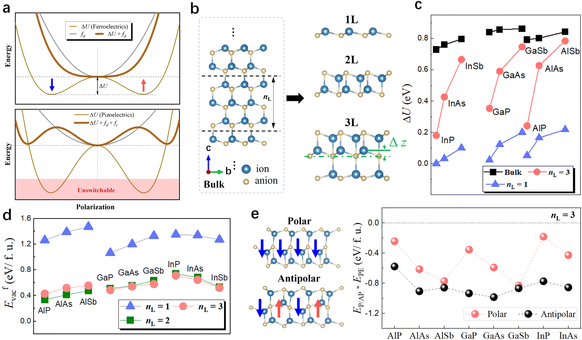 | ||
| Fig. 1 (a) Utilizing the depolarization energy (fd) to soften unswitchable piezoelectrics with large barrier ΔU separating two polar states. The delicate balance between ΔU, fd, and the energy cost (fc) to form antiparallel neighboring dipoles may lead to a triple well in thin films. (b) Construction of ultrathin 2D sheets by cutting wurtzite III–V piezoelectrics along the c plane. The thickness of the sheet is defined as the number (nL) of atomic planes. The right panel shows the optimized structures of monolayer (1L), diatomic layer (2L), and triatomic layer (3L). (c) Energy barrier (ΔU) in bulk and 1L and 3L sheets. (d) Formation energy (Efvac) of 1L, 2L, and 3L sheets. (e) Energy of antipolar (EAP) and polar (EP) phases in 3L sheets relative to the paraelectric (EPE) phase. | ||
We explore our design principle with first-principles density functional theory (DFT) calculations, focusing on ultrathin 2D sheets of wurtzite III–V compounds (III = Al, Ga, In; V = N, P, As). We discover a nonpolar diatomic layer (2L) and a triatomic layer (3L) with spontaneous local inversion symmetry breaking. Specifically for 3L sheets, it can adopt a high-energy polar state with POP and a low-energy antipolar state with neighboring antiparallel dipoles. Interestingly, the polar and antipolar states in 3L AlSb are both dynamically stable, as confirmed by phonon spectrum calculations and ab initio molecular dynamics (AIMD), and these two states are comparable in energy, making 3L AlSb an unusual tristable system that supports both ferroelectricity and antiferroelectricity. Moreover, the electronic degree of freedom is directly coupled to the polar ordering in 3L AlSb, and the tristate switching is accompanied by a metal–semiconductor transition. We propose a 2D homojunction field effect transistor (FET) consisting of 2L and 3L AlSb. The carrier type and density in the semiconducting channel of 2L AlSb can be effectively regulated by the polarization state of 3L AlSb, leading to three distinct and nonvolatile resistance states. The deterministic ferroelectric domain engineering at the nanoscale could be used to pattern the 2L–3L homojunction as high-density periodic arrays of p–n junctions and p–i–n junctions. The proposed 2D sheets of III–V compounds supporting tristable polarization states offer promise for experimental investigation and for the development and design of nonvolatile multistate functional applications such as high-density memory and synaptic electronics.
DFT calculations are performed using Vienna ab initio Simulation Package (VASP).24,25 The interaction between the core ion and electrons is described by the projector augmented wave (PAW) method.26 The PBEsol functional is chosen as the exchange–correlation functional.27 The vacuum layer along the c axis is thicker than 15 Å in the slab model, and dipole correction is employed to remove the spurious interaction between different periodic images. We use an energy cutoff of 700 eV, an 8 × 8 × 1 Monkhorst–Pack k-point mesh, and an energy convergence threshold of 10−8 eV for electronic self-consistent calculations. The convergence criterion for an optimized structure is 10−7 eV in energy. The structural stability at finite temperatures is studied by NVT AIMD simulations using Γ-point sampling with the temperature controlled using a Nosé–Hoover thermostat.28,29 The phonon spectrum is computed using the frozen phonon approach as implemented in Phonopy30 in conjunction with VASP. The key input and output files have been uploaded to a public repository.31
The 2D sheet is constructed by cutting the bulk along the c plane, and the thickness of the film is defined as the number (nL) of atomic planes (Fig. 1b). In the case of monolayers (nL = 1), we find that all nitrides favor the planar structure,32 whereas monolayers of other III–V compounds are buckled honeycomb structures characterized by the presence of POP and small values of ΔU (<0.2 eV, Fig. 1c). We note that III–V buckled honeycomb monolayers have been studied previously with DFT,33–35 though the 2D ferroelectricity was not appreciated. The formation energy per formula unit (f.u.) of an isolated 2D sheet with respect to the bulk counterpart is defined as Efvac = E2D/nL − E3D/N3D, where E2D is the energy of the 2D sheet consisting of nL atomic planes and E3D is the energy of a cell in bulk containing N3D atomic planes. Although several III–V monolayers are potential 2D ferroelectrics featuring small switching barriers, their formation energies are rather large (>0.8 eV per f.u., Fig. 1d), hinting at the difficulty of synthesis in experiments.
When the thickness increases to nL = 2, for III–V compounds (III = Al, Ga, In, V = P, As, Sb), the initial wurtzite-like configuration is no longer stable, and the optimized diatomic layer denoted as 2L acquires the inversion symmetry, thus being nonpolar (Fig. 1b). Further increasing the thickness to nL = 3 surprisingly revives POP. The triatomic layer labeled as 3L has a buckled central layer that breaks the out-of-plane inversion symmetry (Fig. 1b), and the magnitude of the polarization is ≈0.12 × 10⁻¹⁰ C m−1 (see the values in Fig. S1 of the ESI†), which is comparable to those of the out-of-plane polarization of typical 2D ferroelectrics such as α-In2Se3 (0.12 × 10⁻¹⁰ C m−1)8,36 and Co2CF2 (0.117 × 10⁻¹⁰ C m−1).37 Structurally, both 2L and 3L have group-V anions being the outermost surface layers. We note that 3L sheets have much lower formation energies than monolayers albeit with higher ΔU (Fig. 1c and d). This seems to suggest III–V compounds in the 3L form are easier to synthesize but remain unswitchable.
Following the design principle, we investigate the possible competing antipolar phases in 3L sheets. We identify an antipolar phase that has an energy consistently lower than that of the polar phase (Fig. 1e and Fig. S2 in the ESI†). Based on Shirane's energetic criterion on antiferroelectricity, an antiferroelectric is an antipolar crystal with free energy comparable to that of the reference polar crystal that has aligned sublattice local dipoles.38 Therefore, we suggest that 3L sheets of AlSb and GaSb likely host antiferroelectricity as their polar and antipolar phases are close in energy. Below, we demonstrate that 3L AlSb is an unusual tristable system that supports both ferroelectricity and antiferroelectricity.
Fig. 2a presents the phonon spectra of 3L AlSb in polar and antipolar phases, respectively. Since the phonon spectra have no imaginary vibrational frequencies in the whole Brillouin zone, polar and nonpolar phases are dynamically stable and each locates at a local minimum of the potential energy surface. We perform AIMD simulations at elevated temperatures to check the structural stability against larger atomic distortions due to thermal fluctuations. The evolution of the total energy at 400 K during AIMD simulations is shown for both phases in Fig. 2b, revealing no sign of structural destruction or reconstruction. This serves as a strong proof to corroborate the room-temperature stability of 3L AlSb. A defining feature of (anti)ferroelectricity is polarization reversibility. As depicted in Fig. 2c, the barrier separating the polar and antipolar phases obtained with the nudged elastic band (NEB) method is 0.1 eV which is lower than the barrier in conventional perovskite ferroelectrics such as PbTiO3 (0.17 eV),39 indicating a switchable polarization by an external electric field. We note that NEB calculations are performed with lattice constants clamped to the ground-state values of the antipolar phase. In general, when the lattice constants are allowed to relax during the search for the transition state, the identified switching barrier will be lower than the NEB barrier because the material can explore a wider range of configurations and may find lower energy paths. Therefore, we believe the switching barrier computed with NEB is a conservative estimate of polarization reversibility. We conclude that 3L AlSb is a rare 2D material characterized by tristable and electrically switchable polarization states and thus hosts both ferroelectricity and antiferroelectricity.
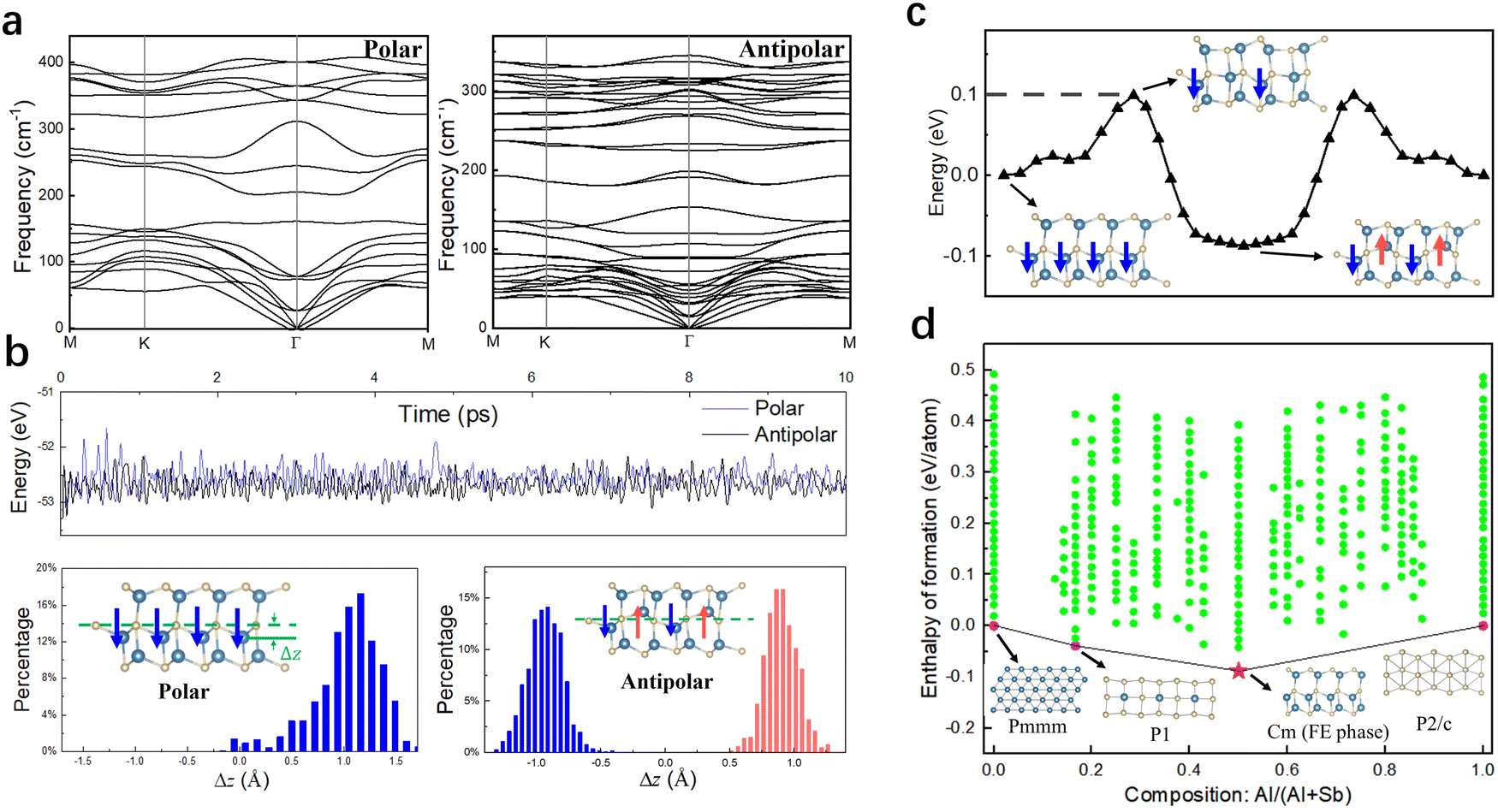 | ||
| Fig. 2 (a) Phonon dispersion relationships of 3L AlSb in the polar phase (left) and antipolar phase (right). (b) AIMD simulations. The top panel shows the energy evolution as a function of time at 400 K. The bottom panel shows the distribution of out-of-plane local displacements (Δz) of Al atoms in the central layer. (c) Minimum energy path obtained with NEB connecting the polar and antipolar phases. (d) Convex hull of AlxSb1−x from the variable-composition evolutionary structure search. | ||
In addition, we perform a structural search using the variable-composition evolutionary algorithm as implemented in USPEX40–42 with a 6-atom slab model confined within 9 Å. Our search algorithm starts with an initial population of 50 structures, and each generation consists of 200 structures produced by heredity (50%), random structure generator (10%), lattice mutation (20%), and atomic mutation (20%); the total number of generations is 192. Fig. 2d compiles the DFT formation enthalpies of all identified 2D crystals for Al1−xSbx. We find that ferroelectric 3L AlSb has a convex hull distance of zero, further supporting its thermodynamic stability and synthesizability.
The emergence of POP in ferroelectric 3L AlSb can be understood by determining the electric free energy (F) of wurtzite AlSb under an open-circuit boundary condition (OCBC) that has D = 0 where D is the electric displacement. For an intermediate configuration, λ, obtained by linear interpolation of the ground-state polar configuration (λ = 1) and the high-symmetry nonpolar configuration (λ = 0, space group: P63/mmc), the free energy F(λ) under D = 0 can be estimated as43,44
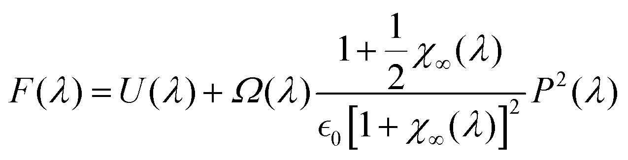 | (1) |
 ) and the second term is the depolarization energy fd associated with the depolarization field under OCBC. All quantities required to evaluate F(λ) are bulk values easily accessible via conventional DFT calculations. This analytical formation of F(λ) has been used to understand the origin of hyperferroelectricity43 in thin films under OCBC.
As shown in Fig. 3a, the potential well of U(λ) is rather deep under SCBC. After introducing the depolarization effect under OCBC, the well becomes shallower and the ground state remains polar as F(λ) reaches the minimum at λ = 0.7. It is noted that eqn (1) does not consider the impact of surface reconstruction or the change in χ∞(λ) with reduced dimension. Nevertheless, the simple analytical model of eqn (1) predicts that AlSb has a low-energy polar state under OCBC, resembling a hyperferroelectric.45 We also plot the DFT energy profile for the ferroelectric–antiferroelectric transition in 3L AlSb in Fig. 3a. By comparing the analytical and DFT results, we suggest the surface reconstruction of 3L AlSb that has group-V anions becoming the outmost surface layers strongly stabilizes the polar phase (λ = 1.1), while the emergence of a low-energy antiferroelectric phase (not captured by the analytical model) is critical for the polarization switchability.
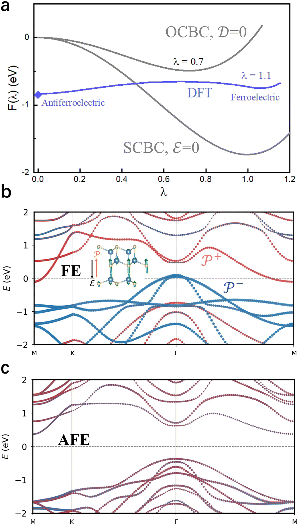 | ||
| Fig. 3 (a) Electric free energy F(λ) of AlSb under SCBC (E = 0) and OCBC (D = 0). The DFT minimum energy pathway (blue line) connecting the ferroelectric (FE) and antiferroelectric (AFE) phases in 3L AlSb is plotted for comparison. Electronic band structures of (b) ferroelectric and (c) antiferroelectric 3L AlSb computed with eACBN0. The ferroelectric phase is a semimetal and the projected band structure has atomic orbital contributions from P− and P+ surfaces colored in blue and red, respectively. The inset in (b) shows the atomic forces induced by an electric field applied against POP, showing that nearly all atoms are affected by the applied field despite the ferroelectric phase being a semimetal. | ||
We now consider the electronic properties of 3L AlSb. Semilocal density functionals such as PBE often underestimate the band gap due to the remnant self-interaction error. To obtain accurate electronic structures of 3L AlSb, we employ a newly developed pseudohybrid Hubbard density functional, extended Agapito–Curtarolo–Buongiorno Nardelli (eACBN0).46–48 The eACBN0 function is a DFT+U+V method with self-consistently computed Hubbard U(V) parameters that account for the onsite (intersite) Coulomb interactions, thus capable of capturing the local variations of Coulomb screening. Particularly for low-dimensional materials, eACBN0 yields better descriptions of the electronic structures than hybrid density functionals such as HSE0649 which assumes fixed dielectric screening.36,47Fig. 3b and c presents the eACBN0 band structures for 3L AlSb in ferroelectric and antiferroelectric phases (see the comparison of eACBN0 and HSE06 band structures in the ESI†). We find that the ferroelectric phase is a semimetal, while the antiferroelectric phase is a semiconductor with a band gap of 0.7 eV. The semimetal nature of the ferroelectric phase is due to the built-in depolarization field that induces band bending50,51 such that the valence band maximum (VBM) and the conduction band minimum (CBM) are dominated by the states of P− and P+ surfaces, respectively (Fig. 3b). Moreover, we compute the field-induced forces (Fig. 3b, inset) and find that nearly all atoms are affected by an applied field. This indicates the (semi)metallic ferroelectric 3L AlSb remains electrically switchable, similar to 2D metallic WTe2.15 In contrast, the antiferroelectric phase has null depolarization field and the band gap is mostly determined by the hybridization of Al-3p and Sb-5p states. The strong coupling between the polarization state and the band gap in 3L AlSb enables an intrinsically voltage-switchable metal–semiconductor transition,52 a useful feature to realize on–off states for device applications.
The ferroelectric field effect transistor (FeFET) comprising a semiconductor as the channel material and a ferroelectric as the gate insulator is an attractive architecture to realize low-power, high-speed, and high-density nonvolatile memory. Our DFT calculations show that 2L AlSb is a nonpolar semiconductor with a band gap of 0.5 eV. Taking advantage of the semiconducting properties of 2L AlSb and the tristable polarization states afforded by 3L AlSb, we propose a 2D homojunction FET using 3L AlSb as the gate insulator and 2L AlSb as the channel material (Fig. 4a). The design based on a homojunction could simplify the fabrication process and improve the device performance over the heterojunction-based device by reducing interfacial defects.
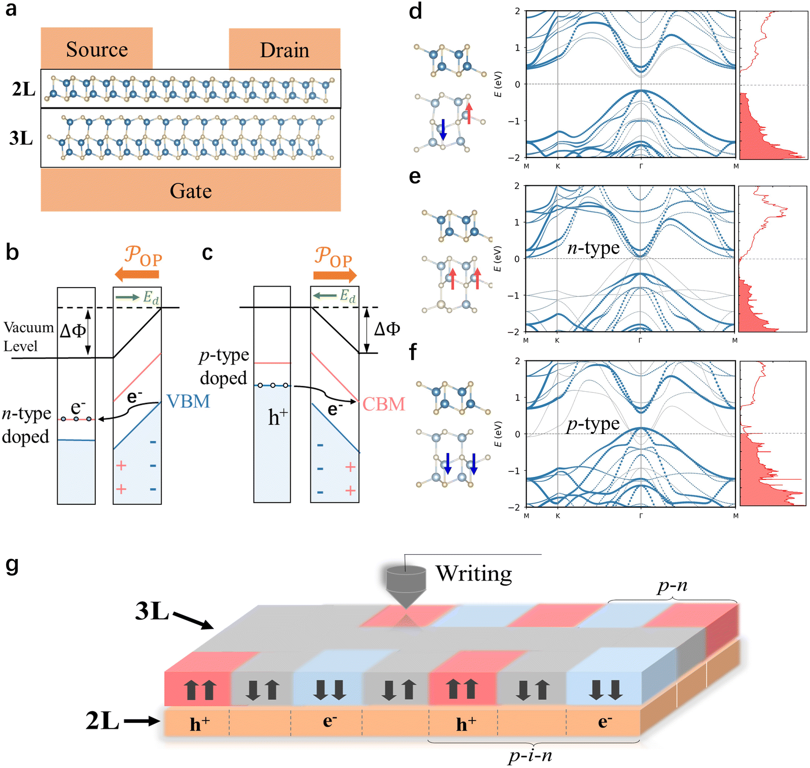 | ||
| Fig. 4 (a) Schematic of a 2D homojunction field effect transistor consisting of semiconducting 2L AlSb and tristable 3L AlSb. (b) Band bending diagrams of the 2L–3L homojunction. The depolarization field Ed in ferroelectric 3L AlSb creates a potential step ΔΦ across the sheet. When POP points toward 2L AlSb, the high-energy electrons transfer from 3L to 2L, making 2L n-type-doped. The polarization reversal will lead to a p-type doped 2L AlSb. Projected electronic band structures and density of states of the 2L–3L homojunction with 3L adopting (d) antiferroelectric, (e) upward polarization, and (f) downward polarization, showing atomic orbital contributions from 2L AlSb. (g) Schematic of voltage-configurable multidomain-determined high-density p–n and p–i–n junction arrays. | ||
We compute the eACBN0 band structures of a 2L–3L homojunction with 3L AlSb adopting different polarization states. The contributions from the states of 2L AlSb are highlighted in the band structures to reveal the electrical properties of the channel. As shown in Fig. 4d–f, the conductivity of 2L AlSb is readily regulated by the polarization state of 3L AlSb. Specifically, when 3L AlSb adopts the antiferroelectric state, the channel consisting of 2L AlSb is a semiconductor with a band gap of ≈0.6 eV (Fig. 4d). When the polarization of 3L AlSb is switched toward 2L AlSb, the band structure of the homojunction reveals an n-type doped 2L AlSb (Fig. 4e). This can be understood from the band diagram (right before the charge transfer) illustrated in Fig. 4b. Because the VBM of 3L AlSb is higher in energy than the CBM of 2L AlSb, the high-energy electrons in 3L AlSb naturally relax to the conduction bands of 2L AlSb, effectively n-type-doping the channel. Finally, in the case where 3L AlSb has the polarization pointing away from 2L AlSb, the channel becomes hole-doped as the electrons in 2L AlSb relax to the CBM of 3L AlSb that is lower in energy (Fig. 4c). Therefore, the tristable polarization states of 3L AlSb create three resistance states of the channel, suitable for nonvolatile multistate functional applications.
In addition, the nanoscale deterministic ferroelectric domain engineering can be employed to configure the 2L–3L homojunction into high-density p–n junction arrays as well as p–i–n junction arrays where the tristable polarization states of 3L AlSb control the carrier type and density in 2L AlSb, as shown in Fig. 4g. The voltage-configurable multidomain pattern offers a platform to design energy-efficient, high-density synaptic electronics and neuromorphic systems.
In summary, we propose a strategy to obtain switchable 2D polar materials with promising compatibility with the main stream semiconductor industry. The depolarization field that is often considered detrimental to ferroelectric properties is used as a physical stressor to convert unswitchable bulk III–V semiconductors to 2D materials with reversible polarization. The delicate competition between the local polarization energy, the global depolarization energy, and the neighboring dipolar coupling in 2D gives rise to a thickness-sensitive phase competition. The triatomic layer of AlSb is demonstrated to exhibit tristable polarization states, thus hosting both ferroelectricity and antiferroelectricity. We have explored the functionalities of AlSb-based 2D homojunctions consisting of diatomic and triatomic layers and predicted the emergence of three distinct and nonvolatile resistance states characterized by different carrier types and densities. The readily regulable doping by the tristable polarization states potentially enables facile fabrication of high-density periodic p–n and p–i–n junctions at the nanoscale for nanoelectric and optoelectronic devices.
Conflicts of interest
There are no conflicts to declare.Acknowledgements
C. K. and S. L. acknowledge the support from Westlake Education Foundation. The computational resources were provided by Westlake HPC Center.References
- J. F. Scott, Applications of modern ferroelectrics, Science, 2007, 315, 954 CrossRef CAS PubMed.
- L. W. Martin and A. M. Rappe, Thin-film ferroelectric materials and their applications, Nat. Rev. Mater., 2016, 2, 16087 CrossRef.
- T. Mikolajick, S. Slesazeck, H. Mulaosmanovic, M. H. Park, S. Fichtner, P. D. Lomenzo, M. Hoffmann and U. Schroeder, Next generation ferroelectric materials for semiconductor process integration and their applications, J. Appl. Phys., 2021, 129, 100901 CrossRef CAS.
- M. Wu and P. Jena, The rise of two-dimensional van der Waals ferroelectrics, WIREs Comput. Mol. Sci., 2018, 8, e1365 Search PubMed.
- Z. Guan, H. Hu, X. Shen, P. Xiang, N. Zhong, J. Chu and C. Duan, Recent progress in two-dimensional ferroelectric materials, Adv. Electron. Mater., 2019, 6, 1900818 CrossRef.
- M. Kruse, U. Petralanda, M. N. Gjerding, K. W. Jacobsen, K. S. Thygesen and T. Olsen, Two-dimensional ferroelectrics from high throughput computational screening, arXiv, 2022, preprint, arxiv:2209.13911v1, DOI:10.48550/arxiv:2209.13911v1.
- F. Liu, L. You, K. L. Seyler, X. Li, P. Yu, J. Lin, X. Wang, J. Zhou, H. Wang, H. He, S. T. Pantelides, W. Zhou, P. Sharma, X. Xu, P. M. Ajayan, J. Wang and Z. Liu, Room-temperature ferroelectricity in CuInP2S6 ultrathin flakes, Nat. Commun., 2016, 7, 12357 CrossRef CAS PubMed.
- W. Ding, J. Zhu, Z. Wang, Y. Gao, D. Xiao, Y. Gu, Z. Zhang and W. Zhu, Prediction of intrinsic two-dimensional ferroelectrics in In2Se3 and other III2-VI3 van der Waals materials, Nat. Commun., 2017, 8, 14956 CrossRef CAS PubMed.
- Y. Zhou, D. Wu, Y. Zhu, Y. Cho, Q. He, X. Yang, K. Herrera, Z. Chu, Y. Han, M. C. Downer, H. Peng and K. Lai, Out-of-plane piezoelectricity and ferroelectricity in layered α-In2Se3 nanoflakes, Nano Lett., 2017, 17, 5508 CrossRef CAS PubMed.
- C. Cui, W.-J. Hu, X. Yan, C. Addiego, W. Gao, Y. Wang, Z. Wang, L. Li, Y. Cheng, P. Li, X. Zhang, H. N. Alshareef, T. Wu, W. Zhu, X. Pan and L.-J. Li, Intercorrelated in-plane and out-of-plane ferroelectricity in ultrathin two-dimensional layered semiconductor In2Se3, Nano Lett., 2018, 18, 1253 CrossRef CAS PubMed.
- J. Xiao, H. Zhu, Y. Wang, W. Feng, Y. Hu, A. Dasgupta, Y. Han, Y. Wang, D. A. Muller, L. W. Martin, P. Hu and X. Zhang, Intrinsic two-dimensional ferroelectricity with dipole locking, Phys. Rev. Lett., 2018, 120, 227601 CrossRef CAS PubMed.
- S. M. Poh, S. J. R. Tan, H. Wang, P. Song, I. H. Abidi, X. Zhao, J. Dan, J. Chen, Z. Luo, S. J. Pennycook, A. H. C. Neto and K. P. Loh, Molecular-beam epitaxy of two-dimensional In2Se3 and its giant electroresistance switching in ferroresistive memory junction, Nano Lett., 2018, 18, 6340 CrossRef CAS PubMed.
- S. Wan, Y. Li, W. Li, X. Mao, W. Zhu and H. Zeng, Room-temperature ferroelectricity and a switchable diode effect in two-dimensional α-In2Se3 thin layers, Nanoscale, 2018, 10, 14885 RSC.
- S. Yuan, X. Luo, H. L. Chan, C. Xiao, Y. Dai, M. Xie and J. Hao, Room-temperature ferroelectricity in MoTe2 down to the atomic monolayer limit, Nat. Commun., 2019, 10, 1775 CrossRef PubMed.
- Z. Fei, W. Zhao, T. A. Palomaki, B. Sun, M. K. Miller, Z. Zhao, J. Yan, X. Xu and D. H. Cobden, Ferroelectric switching of a two-dimensional metal, Nature, 2018, 560, 336 CrossRef CAS PubMed.
- K. Ferri, S. Bachu, W. Zhu, M. Imperatore, J. Hayden, N. Alem, N. Giebink, S. Trolier-McKinstry and J.-P. Maria, Ferroelectrics everywhere: Ferroelectricity in magnesium substituted zinc oxide thin films, J. Appl. Phys., 2021, 130, 044101 CrossRef CAS.
- S. Fichtner, N. Wolff, F. Lofink, L. Kienle and B. Wagner, AlScN: A III-V semiconductor based ferroelectric, J. Appl. Phys., 2019, 125, 114103 CrossRef.
- J. Jeong, S. K. Kim, J. Kim, D.-M. Geum, D. Kim, E. Jo, H. Jeong, J. Park, J.-H. Jang, S. Choi, I. Kwon and S. Kim, Heterogeneous and monolithic 3d integration of III–V-based radio frequency devices on Si CMOS circuits, ACS Nano, 2022, 16, 9031 CrossRef CAS PubMed.
- S. Chen, W. Li, J. Wu, Q. Jiang, M. Tang, S. Shutts, S. N. Elliott, A. Sobiesierski, A. J. Seeds, I. Ross, P. M. Smowton and H. Liu, Electrically pumped continuous-wave III–V quantum dot lasers on silicon, Nat. Photonics, 2016, 10, 307 CrossRef CAS.
- I. Vurgaftman, J. R. Meyer and L. R. Ram-Mohan, Band parameters for III–V compound semiconductors and their alloys, J. Appl. Phys., 2001, 89, 5815 CrossRef CAS.
- W. Yang, Y. Li, F. Meng, H. Yu, M. Wang, P. Wang, G. Luo, X. Zhou and J. Pan, III–V compound materials and lasers on silicon, J. Semicond., 2019, 40, 101305 CrossRef CAS.
- III–V on Silicon, https://www.iqep.com/innovation/new-technology-platforms/iii-v-on-silicon/, (accessed on 2023–12).
- J. Junquera and P. Ghosez, Critical thickness for ferroelectricity in perovskite ultrathin films, Nature, 2003, 422, 506 CrossRef CAS PubMed.
- G. Kresse and J. Furthmuller, Efficient iterative schemes for ab initio total-energy calculations using a plane-wave basis set, Phys. Rev. B: Condens. Matter Mater. Phys., 1996, 54, 11169 CrossRef CAS PubMed.
- G. Kresse and J. Furthmuller, Efficiency of ab-initio total energy calculations for metals and semiconductors using a plane-wave basis set, Comput. Mater. Sci., 1996, 6, 15 CrossRef CAS.
- P. E. Blochl, Projector augmented-wave method, Phys. Rev. B: Condens. Matter Mater. Phys., 1994, 50, 17953 CrossRef PubMed.
- J. P. Perdew, A. Ruzsinszky, G. I. Csonka, O. A. Vydrov, G. E. Scuseria, L. A. Constantin, X. Zhou and K. Burke, Restoring the density-gradient expansion for exchange in solids and surfaces, Phys. Rev. Lett., 2008, 100, 136406 CrossRef PubMed.
- S. Nose, A unified formulation of the constant temperature molecular dynamics methods, J. Chem. Phys., 1984, 81, 511 CrossRef CAS.
- W. G. Hoover, Canonical dynamics: Equilibrium phase-space distributions, Phys. Rev. A: At., Mol., Opt. Phys., 1985, 31, 1695 CrossRef PubMed.
- A. Togo and I. Tanaka, First principles phonon calculations in materials science, Scr. Mater., 2015, 108, 1 CrossRef CAS.
- C. Ke, kechangming/2D-III-V-AFE-FE: v1.0.0 (2023), DOI:10.5281/zenodo.7703597, (accessed on 2023-03-07).
- D. Wu, M. G. Lagally and F. Liu, Stabilizing graphitic thin films of wurtzite materials by epitaxial strain, Phys. Rev. Lett., 2011, 107, 236101 CrossRef PubMed.
- H. Sahin, S. Cahangirov, M. Topsakal, E. Bekaroglu, E. Akturk, R. T. Senger and S. Ciraci, Monolayer honeycomb structures of group-IV elements and III-V binary compounds: Firstprinciples calculations, Phys. Rev. B: Condens. Matter Mater. Phys., 2009, 80, 155453 CrossRef.
- H. L. Zhuang, A. K. Singh and R. G. Hennig, Computational discovery of single-layer III-V materials, Phys. Rev. B: Condens. Matter Mater. Phys., 2013, 87, 165415 CrossRef.
- R. Gao and Y. Gao, Piezoelectricity in two-dimensional group III-V buckled honeycomb monolayers, Phys. Status Solidi RRL, 2017, 11, 1600412 CrossRef.
- J. Huang, S.-H. Lee, Y.-W. Son, A. Supka and S. Liu, First-principles study of twodimensional ferroelectrics using self-consistent hubbard parameters, Phys. Rev. B, 2020, 102, 165157 CrossRef CAS.
- C. Huang, J. Zhou, H. Sun, F. Wu, Y. Hou and E. Kan, Toward room-temperature electrical control of magnetic order in multiferroic van der Waals materials, Nano Lett., 2022, 22, 5191 CrossRef CAS PubMed.
- G. Shirane, Ferroelectricity and antiferroelectricity in ceramic PbZrO3 containing Ba or Sr, Phys. Rev., 1952, 86, 219 CrossRef CAS.
- J. Huang, Y. Hu and S. Liu, Origin of ferroelectricity in magnesium-doped zinc oxide, Phys. Rev. B, 2022, 106, 144106 CrossRef CAS.
- A. R. Oganov and C. W. Glass, Crystal structure prediction using ab initio evolutionary techniques: Principles and applications, J. Chem. Phys., 2006, 124, 244704 CrossRef PubMed.
- A. O. Lyakhov, A. R. Oganov, H. T. Stokes and Q. Zhu, New developments in evolutionary structure prediction algorithm USPEX, Comput. Phys. Commun., 2013, 184, 1172 CrossRef CAS.
- A. R. Oganov, A. O. Lyakhov and M. Valle, How evolutionary crystal structure prediction works—and why, Acc. Chem. Res., 2011, 44, 227 CrossRef CAS PubMed.
- R. Adhikari and H. Fu, Hyperferroelectricity in zno: Evidence from analytic formulation and numerical calculations, Phys. Rev. B, 2019, 99, 104101 CrossRef CAS.
- S. Qiu, L. Ma, S. Liu and H. Fu, Possible existence of tristable polarization states in linbo3 under an open-circuit boundary condition, Phys. Rev. B, 2021, 104, 064112 CrossRef CAS.
- K. F. Garrity, K. M. Rabe and D. Vanderbilt, Hyperferroelectrics: Proper ferroelectrics with persistent polarization, Phys. Rev. Lett., 2014, 112, 127601 CrossRef PubMed.
- L. A. Agapito, A. Ferretti, A. Calzolari, S. Curtarolo and M. B. Nardelli, Effective and accurate representation of extended Bloch states on finite Hilbert spaces, Phys. Rev. B: Condens. Matter Mater. Phys., 2013, 88, 165127 CrossRef.
- S.-H. Lee and Y.-W. Son, First-principles approach with a pseudohybrid density functional for extended Hubbard interactions, Phys. Rev. Res., 2020, 2, 043410 CrossRef CAS.
- N. Tancogne-Dejean and A. Rubio, Parameter-free hybridlike functional based on an extended Hubbard model: DFT+U+V, Phys. Rev. B, 2020, 102, 155117 CrossRef CAS.
- A. V. Krukau, O. A. Vydrov, A. F. Izmaylov and G. E. Scuseria, Influence of the exchange screening parameter on the performance of screened hybrid functionals, J. Chem. Phys., 2006, 125, 224106 CrossRef PubMed.
- C. Ke, J. Huang and S. Liu, Two-dimensional ferroelectric metal for electrocatalysis, Mater. Horiz., 2021, 8, 3387 RSC.
- J. Huang, X. Duan, S. Jeon, Y. Kim, J. Zhou, J. Li and S. Liu, On-demand quantum spin hall insulators controlled by two-dimensional ferroelectricity, Mater. Horiz., 2022, 9, 1440 RSC.
- X. Duan, J. Huang, B. Xu and S. Liu, A two-dimensional multiferroic metal with voltagetunable magnetization and metallicity, Mater. Horiz., 2021, 8, 2316 RSC.
Footnote |
| † Electronic supplementary information (ESI) available. See DOI: https://doi.org/10.1039/d3nh00026e |
| This journal is © The Royal Society of Chemistry 2023 |