
Nanoscale compositional segregation in epitaxial AlScN on Si (111)
Xiaoman
Zhang
a,
Eric A.
Stach
 bc,
W. J.
Meng
*a and
Andrew C.
Meng
*d
bc,
W. J.
Meng
*a and
Andrew C.
Meng
*d
aMechanical and Industrial Engineering Dept., Louisiana State University, Baton Rouge, LA, USA 70803. E-mail: wmeng1@lsu.edu
bMaterials Science and Engineering Dept., University of Pennsylvania, Philadelphia, PA, USA 19104
cLaboratory for Research on the Structure of Matter, University of Pennsylvania, Philadelphia, Pennsylvania, USA 19104
dPhysics and Astronomy Dept., University of Missouri, Columbia, MO, USA 65211. E-mail: acmeng@missouri.edu
First published on 6th March 2023
Abstract
We report the growth of epitaxial wurtzite AlScN thin films on Si (111) substrates with a wide range of Sc concentrations using ultra-high vacuum reactive sputtering. Sc alloying in AlN enhances piezoelectricity and induces ferroelectricity, and epitaxial thin films facilitate systematic structure-based investigations of this important and emerging class of materials. Two main effects are observed as a function of increasing Sc concentration. First, increasing crystalline disorder is observed together with a structural transition from wurtzite to rocksalt at ∼30 at% Sc. Second, nanoscale compositional segregation consistent with spinodal decomposition occurs at intermediate compositions, before the wurtzite to rocksalt phase boundary is reached. Lamellar features arising from composition fluctuations are correlated with polarization domains in AlScN, suggesting that composition segregation can influence ferroelectric properties. The present results provide a route to the creation of single crystal AlScN films on Si (111), as well as a means for self-assembled composition modulation.
New conceptsWhile recent studies on wurtzitic aluminum scandium nitride (AlScN) ferroelectrics show significant promise for new computing hardware applications, there remain many challenges stemming from an incomplete understanding of the complex structure–property relationship in these materials relevant to device performance issues of practical concern, for example electrical leakage. We take a different approach: by using ultra-high vacuum vapor phase growth at high temperatures to achieve epitaxial AlScN thin films on Si (111) substrates, structural parameter variations are minimized. Our aim is a systematic investigation of structure–property relationships towards improved structural parameter control as compared to commonly studied polycrystalline films. Characterization of epitaxial AlScN films shows several levels of structural disorder: a diffuse epitaxial interface, significant mosaic tilt and twist that increases with increasing Sc composition, and nanoscale compositional segregation at intermediate Sc compositions consistent with spinodal decomposition. Compositionally segregated lamellae are concurrent with maps of electrical polarization. The present study demonstrates increased structural disorder with increasing Sc composition in AlScN, and highlights the connection between structural disorder and polarization domains. Epitaxial AlScN on Si (111) is a potential model system to systematically investigate structure–property relationships in wurtzitic alloy ferroelectrics and a promising platform for materials discovery for other non-conventional ferroelectrics. |
1. Introduction
There is significant current interest in ferroelectric aluminum nitride-based alloys. These materials are being explored for potential ferroelectric or piezoelectric device applications. As ferroelectric materials, AlScN and AlBN exhibit significantly higher remanent polarizations compared to established materials such as lead zirconium titanate, and remain stable at temperatures greater than 1000 °C.1,2 As piezoelectric materials, nitride-based alloys with various alloying components have been found to exhibit significantly enhanced piezoelectric constants and can be grown using processes compatible with Si CMOS for state-of-the-art MEMS devices.3–6 Because electrical leakage is a major challenge in AlN-based ferroelectrics and piezoelectrics, many recent studies have highlighted methodologies to improve device stability by mitigating leakage currents and dielectric breakdown.7–13 Some reports of abnormally oriented grains suggest that there are structural origins underlying problems with device performance.14–16A significant fraction of ferroelectric/piezoelectric devices reported in the current literature are fabricated from columnar nanocrystals, making a systematic structure-based study difficult. One difficulty stems from the nonuniformity of poly-/nano-crystalline samples, for which effects of multiple grain orientations and grain boundaries are difficult to evaluate. Another difficulty stems from the importance of isolating structural variables to determine the causal relationship for device behavior, including grain size, crystallographic orientation, and alloy composition. Because ferroelectric and piezoelectric response are influenced by many structural variables, minimizing structural variation through investigation of epitaxial thin films provides one route towards a better understanding of the structure–property relationship.
Hetero-epitaxial growth of AlN thin films has been known for at least four decades, through reactive sputtering,17 chemical vapor deposition,18 or molecular beam epitaxy.19 While epitaxial growth of AlScN has been shown on iso-structural GaN substrates20,21 and on sapphire substrates,22 growth on Si substrates is advantageous due to the lower cost and potential integration with electronics. There are also a number of reports of sputtered epitaxial AlScN films.23–25 Here, we report the growth of epitaxial AlScN thin films on Si (111) substrates using ultra-high vacuum (UHV) reactive sputtering. This approach fixes the in-plane orientation of AlScN with respect to the Si wafer, and has been demonstrated on epitaxial Mo/AlN templates on Si (111).26 While the films remain epitaxial with increasing Sc concentration, significant structural disorder arises as the material undergoes a transition from a wurtzite structure on the pure AlN end to a rocksalt structure on the pure ScN end. Epitaxial AlScN films grown on Si provide a material platform to systematically investigate the structure–property relationship of wurtzite-based compound ferroelectrics and piezoelectrics.
At intermediate Sc concentrations, nanoscale compositional segregation between Al and Sc is observed in epitaxial AlScN films on Si (111) (vide infra).27 In systems exhibiting a miscibility gap, uphill diffusion can occur in the unstable region of the phase diagram, known as spinodal decomposition. While it is known that AlN and ScN have a positive enthalpy of mixing,28 this type of compositional segregation has not been commonly reported. There has been one report of spinodal decomposition in co-sputtered AlScN, but this has only been observed when the Sc concentration is above 50 at%.27 Interestingly, compositional modulation has been proposed to improve dielectric breakdown strength in AlScN.8 Controlled spinodal decomposition in AlScN alloys may provide an alternative means by which compositional modulation can be achieved.
2. Materials and methods
AlN and AlScN thin films were grown in an UHV dc magnetron sputter deposition system with base pressure below 5 × 10⁻¹⁰ Torr. The deposition system consists of a growth chamber pumped by one turbomolecular pump and one cryogenic pump and a turbomolecular-pumped load-lock chamber. The growth chamber accommodates 75 mm sputter sources for Al (99.99%) and Sc (99.99%). Low resistivity As-doped n+-Si (111) substrates, with diameter of 50 mm and resistivities in the range of 0.001–0.005 Ω cm, were cleaned ultrasonically in acetone and ethanol, etched alternately in 10% (v/v) HF and 40% (v/v) HNO3, blown dry with dry N2, mounted onto a Mo holder, evacuated in the load-lock chamber, and transferred into the growth chamber. The front side of the Si wafers faced incoming vapor fluxes while the back side faced a SiC-based electric heater. The actual substrate temperature was calibrated through direct optical access infrared pyrometry, with the Si emissivity set at 0.68. The Si wafers were heated in the growth chamber to ∼800 °C for 30 min prior to film deposition at the same temperature. All growths were carried out in an Ar/N2 mixture, with an input Ar (99.999%) flow rate of 20 sccm. For AlN films, epitaxial films were achieved using N2 (99.999%) flow rates greater than 2.5 sccm. For lower N2 flow rates, metallic Al is observed, and for N2 flow rates higher than 8 sccm, the growth rate decreases significantly. The targets were sputtered in a dc mode, and a −40 V substrate bias was applied. Growth of AlN and AlScN films occurred with the Al target operated at 1.2 A and varying Sc target currents (0 A, 0.4 A, 0.54 A, and 0.7 A) to change the Sc concentration. For these Sc gun currents, N2 flow rates of 5.0, 6.0, 6.0, and 6.2 sccm were used, respectively, to ensure sufficient nitrogen incorporation into the films. After growth, the specimens were allowed to cool to room temperature before being transferred out of the growth chamber.The composition and crystal quality of the AlN/Si (111) and AlScN/Si (111) specimens were characterized by X-ray diffraction (XRD, PANalytical Empyrean), and Scanning/Transmission Electron Microscopy (S/TEM, JEOL NEOARM 30–200 kV, JEOL JEM-F200). The JEOL NEOARM 30–200 kV is equipped with two large-area silicon drift detectors (SDD) for EDS with 1.7 steradian solid angle for X-ray Energy Dispersive Spectroscopy (EDS) measurements. For XRD, the incident Cu Kα X-ray passed through a four-bounce Ge(220) monochromator, selecting an incident wavelength λ = 1.540598 Å. The specimens were mounted on a χ–ϕ–x–y–z stage, allowing symmetric θ/2θ, asymmetric ϕ, ω rocking curve, and reciprocal space mapping (RSM) scans to be performed. Scattering signals were collected with a PIXcel 3D detector with and without a three-bounce Ge(220) analyzer crystal in the diffracted beam path. TEM samples were prepared using a ThermoFisher Helios G4 dual beam Xe plasma focused ion beam/scanning electron microscope (PFIB/SEM). Electron beam induced deposition of Pt, followed by ion beam induced deposition of Pt was used to protect the sample from the ion beam. The sample was thinned at successively lower accelerating voltages, with final thinning performed at 8 kV. All TEM experiments were carried out at a 200 kV accelerating voltage. Probe aberration corrected STEM was performed using the JEOL NEOARM 30–200 kV using probe size 6C and a 40 μm condenser aperture, leading to ∼120 pA probe current. EDS mapping in STEM was performed using the JEOL JEM-F200 equipped with dual silicon-drift detector EDS systems with a large solid angle (1.7 sr) using probe size 7 and a 40 μm condenser aperture, leading to ∼60 pA probe current.
The JEOL JEM-F200 S/TEM instrument was used in the scanning transmission (STEM) mode for 4D-STEM diffraction experiments. For STEM image collection, a 40 μm condenser aperture was used with a probe size of 7, giving approximately 60 pA of probe current (∼1.6 Å probe size). Diffraction patterns in 4D-STEM were collected using a 10 μm condenser aperture in order to minimize overlap in diffraction disks; a 0.04 s dwell time was used to collect a 1k × 1k diffraction pattern at each pixel using a Gatan OneView in situ CCD camera (4k × 4k resolution) with 4× software binning. Drift correction was performed once every row with the high-angle annular dark field (HAADF) detector inserted while the diffraction patterns were being collected. Differential phase contrast maps were performed by analyzing beam displacement using the center-of-mass method. Thus, for each diffraction pattern, the beam displacement coordinates are obtained through the integrals of each coordinate weighted by the intensity distribution function.
3. Results
The Al and Sc concentrations within AlScN films deposited on Si (111) substrates using UHV reactive sputtering were determined through EDS in STEM (Fig. 1(e), also vide infra). The Sc concentrations of the AlScN films are ∼0 at%, 19 at%, 31 at%, and 37 at%. The structure of AlN and AlScN films with varying Sc concentrations was characterized using XRD. The symmetric θ/2θ scans are depicted in Fig. 1(a). In addition to the Si substrate reflections, only one family of AlScN reflections are observed, which can be indexed to wurtzite (0002) and (0004) when also considering electron diffraction data (vide infra). This indicates that the AlN and AlScN films are completely textured with AlScN (0001)//Si (111). The corresponding asymmetric 360° ϕ scans for the wurtzite (10![[1 with combining macron]](https://www.rsc.org/images/entities/char_0031_0304.gif) 3) reflection of AlN/AlScN films and the Si (513) reflection are shown in Fig. 1(b). Six AlScN (103) peaks are observed at 60° intervals for AlN and AlScN, with each peak in the middle between two Si (513) peaks, offset by 30°. Fig. 1(a and b) show that the AlN and AlScN films adopt the wurtzite structure and are epitaxial, with the film/substrate orientation relationship of AlScN (0001)//Si (111) and AlScN (11
3) reflection of AlN/AlScN films and the Si (513) reflection are shown in Fig. 1(b). Six AlScN (103) peaks are observed at 60° intervals for AlN and AlScN, with each peak in the middle between two Si (513) peaks, offset by 30°. Fig. 1(a and b) show that the AlN and AlScN films adopt the wurtzite structure and are epitaxial, with the film/substrate orientation relationship of AlScN (0001)//Si (111) and AlScN (11![[2 with combining macron]](https://www.rsc.org/images/entities/char_0032_0304.gif) 0)//Si (110). As a function of increasing Sc concentration, intensities of the wurtzite peaks decrease in both the symmetric θ/2θ scans and the asymmetric ϕ scans. Fig. 1(c) replots the symmetric θ/2θ scan data around the AlN/AlScN (0002) reflection. As the Sc concentration increases, in addition to the obvious decrease in the (0002) diffraction peak intensity, the peak width also increases significantly. The symmetric shape of the AlN (0002) peak evolves into one with two shoulders with 2θ values respectively lower and higher than that corresponding to the peak intensity. For the Al0.63Sc0.37N film, the two shoulders reach 2θ values of ∼34.5° and ∼38°, respectively, with the peak 2θ value at ∼35.59°. This indicates the existence of significant variations in the local out-of-plane lattice spacing d(0002) from ∼0.24 nm to ∼0.26 nm, with that corresponding to the peak at 0.252 nm. Fig. 1(d) shows measured ω rocking curves for AlN and the AlScN film with 19 at% Sc. Sc alloying increases the rocking curve full-width-at-half-maximum (FWHM) from ∼1.8° to ∼8.4°. For higher Sc concentrations, the ω rocking curves are even broader.
0)//Si (110). As a function of increasing Sc concentration, intensities of the wurtzite peaks decrease in both the symmetric θ/2θ scans and the asymmetric ϕ scans. Fig. 1(c) replots the symmetric θ/2θ scan data around the AlN/AlScN (0002) reflection. As the Sc concentration increases, in addition to the obvious decrease in the (0002) diffraction peak intensity, the peak width also increases significantly. The symmetric shape of the AlN (0002) peak evolves into one with two shoulders with 2θ values respectively lower and higher than that corresponding to the peak intensity. For the Al0.63Sc0.37N film, the two shoulders reach 2θ values of ∼34.5° and ∼38°, respectively, with the peak 2θ value at ∼35.59°. This indicates the existence of significant variations in the local out-of-plane lattice spacing d(0002) from ∼0.24 nm to ∼0.26 nm, with that corresponding to the peak at 0.252 nm. Fig. 1(d) shows measured ω rocking curves for AlN and the AlScN film with 19 at% Sc. Sc alloying increases the rocking curve full-width-at-half-maximum (FWHM) from ∼1.8° to ∼8.4°. For higher Sc concentrations, the ω rocking curves are even broader.
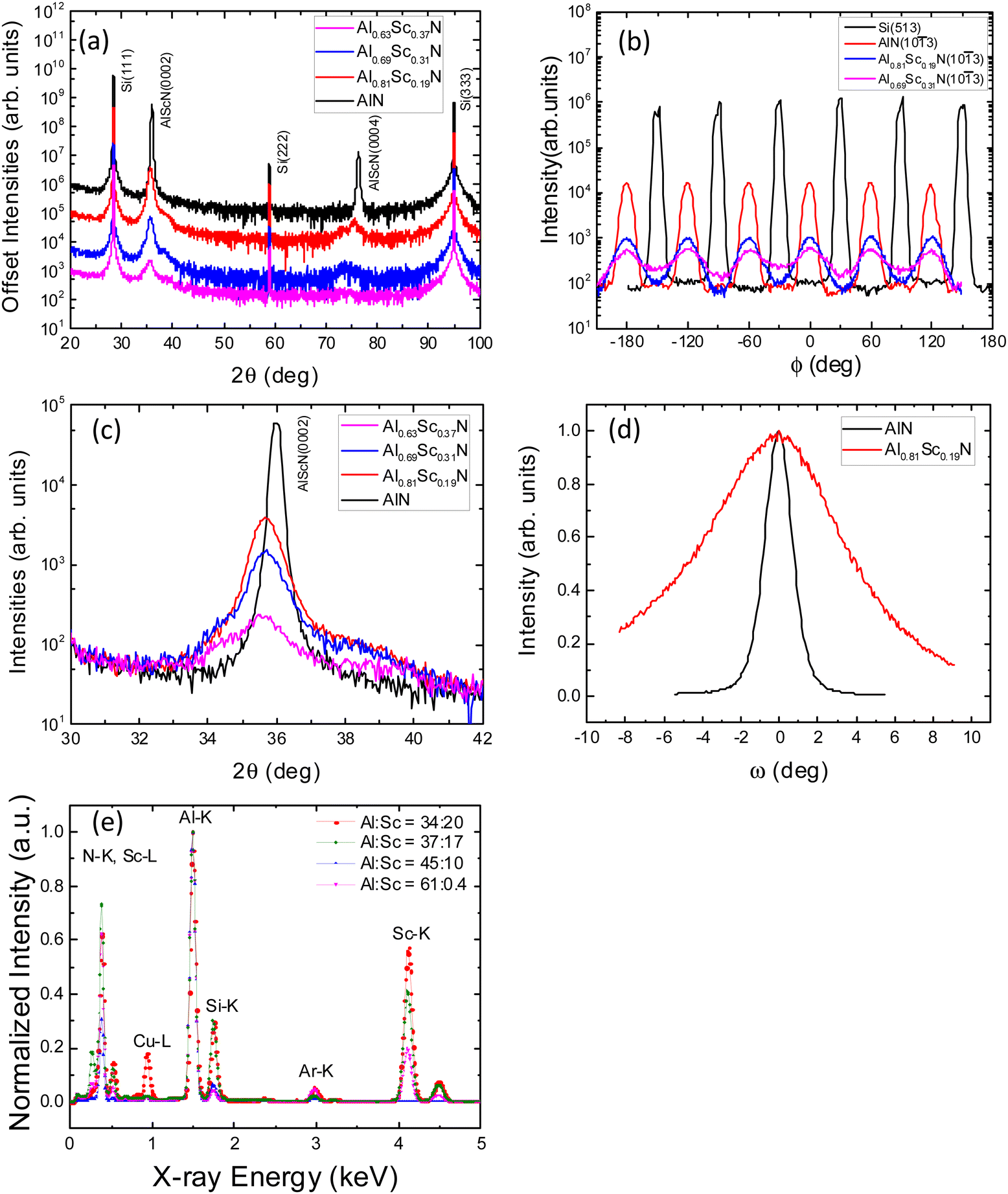 | ||
| Fig. 1 X-Ray characterization of AlN and AlScN thin films grown on Si (111): (a) θ/2θ scans of AlN (black) and AlScN of various Sc concentrations (red, blue, magenta) with an arbitrary intensity offset between datasets applied for clarity; (b) 360° ϕ-scans on the (513) reflection of Si (black) and (103) reflections of AlN (red) and AlScN (blue, magenta); (c) a magnified view around the wurtzite (0002) peak of θ/2θ scans [AlN (black), AlScN of various Sc concentrations (red, blue, magenta)]; (d) ω rocking curve scans on (0002) reflections of AlN (black) and AlScN with 19 at% Sc (red); (e) STEM EDS spectra of AlN and AlScN films. | ||
Fig. 2 shows results of XRD reciprocal space mapping (RSM) scans. Diffracted intensity distributions are plotted around the Si (111) and wurtzite (0002) reflections, with the Qy-direction parallel to the growth direction and the Qx-direction along the in-plane direction. RSM data around the Si (111) reflections of different AlN and AlScN specimens are consistent, a typical one of which is shown in Fig. 2(a). Measured value of the peak FWHM is consistently ∼0.8 × 10⁻⁴ reciprocal lattice unit (rlu) in both x and y directions, with 1 rlu = 2/λ = 12.98187 nm−1. As shown in Fig. 2(b and c), the (0002) peak intensity distributions in reciprocal space are much more extended. The width of the (0002) peak in the in-plane (Qx) direction is ∼100 × 10−4 rlu for the AlN specimen and ∼400 × 10−4 rlu for the AlScN specimen. This increased reciprocal space width in the in-plane-direction when Sc is incorporated into AlN is consistent with the ω rocking curve data shown in Fig. 1(d). Furthermore, the significantly larger (0002) peak width in the out-of-plane (Qy) direction for the AlScN specimen as compared to that for the AlN specimen, >50 × 10−4 rlu vs. < 20 × 10−4 rlu, is also consistent with the θ/2θ scan data shown in Fig. 1(c). Data shown in Fig. 1 and 2 indicate that, as increasing amounts of Sc is added to AlN, the mosaic spread of the AlScN film increases and the out-of-plane lattice spacing d(0002) exhibits increased variation.
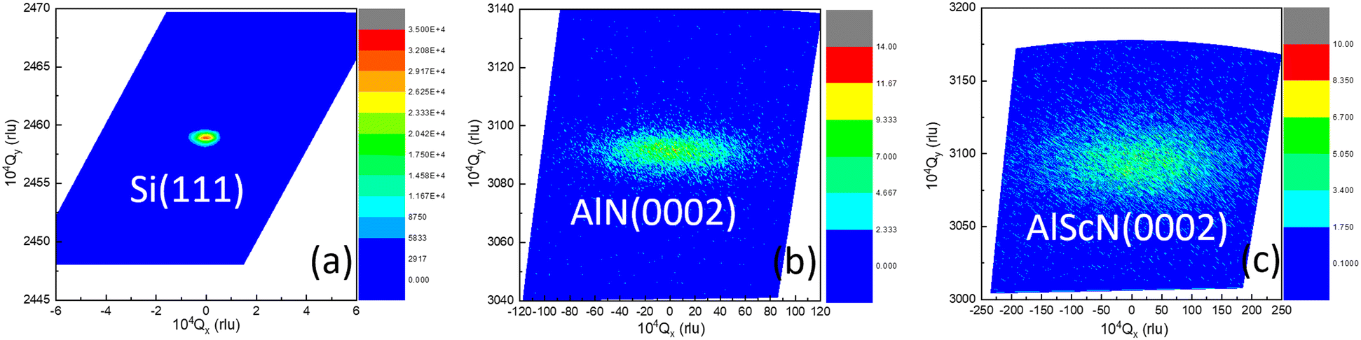 | ||
| Fig. 2 XRD reciprocal space mapping (RSM) of AlN and AlScN with 19 at% Sc: (a) typical intensity distribution around the Si (111) reflection; (b) intensity distribution around the wurtzite (0002) reflection of the AlN specimen; (c) intensity distribution around the wurtzite (0002) reflection of the AlScN specimen with 19 at% Sc. | ||
Further structural characterization of as-deposited AlN and AlScN films was conducted with TEM, through high resolution phase contrast imaging and selected area electron diffraction (SAED). The phase contrast image shown in Fig. 3(a) shows clear lattice fringes in the AlN film and the Si substrate. The associated SAED from the imaged area shows a superposition of Si [10] and wurtzite [20] zone axis patterns. The presence of a strong wurtzite (0001) double diffraction spot provides clear evidence that the AlN film adopts the wurtzite structure. Data shown in Fig. 3(a) confirms that the AlN film is wurtzitic and epitaxial on Si (111), with Si (111)//AlN (0001) and Si (10)//AlN (110), in agreement with the XRD data shown in Fig. 1. Fig. 3(b) shows that the Al0.81Sc0.19N film continues to adopt the wurtzite structure and is epitaxial on Si (111), with the same orientational relationship of Si (111)//AlScN (0001) and Si (10)//AlScN (110). While the phase contrast image continues to show lattice fringes in both the AlScN film and the Si substrate, the associated SAED indicates increased structural disorder. The increased intensity spread perpendicular to the growth direction for the wurtzite (0002) diffraction spot indicates increased film mosaic spread, consistent with information from the XRD data shown in Fig. 1 and 2. The intensity of the wurtzite (0001) double diffraction spot also decreases significantly as compared to that of the AlN film, shown in Fig. 3(a).
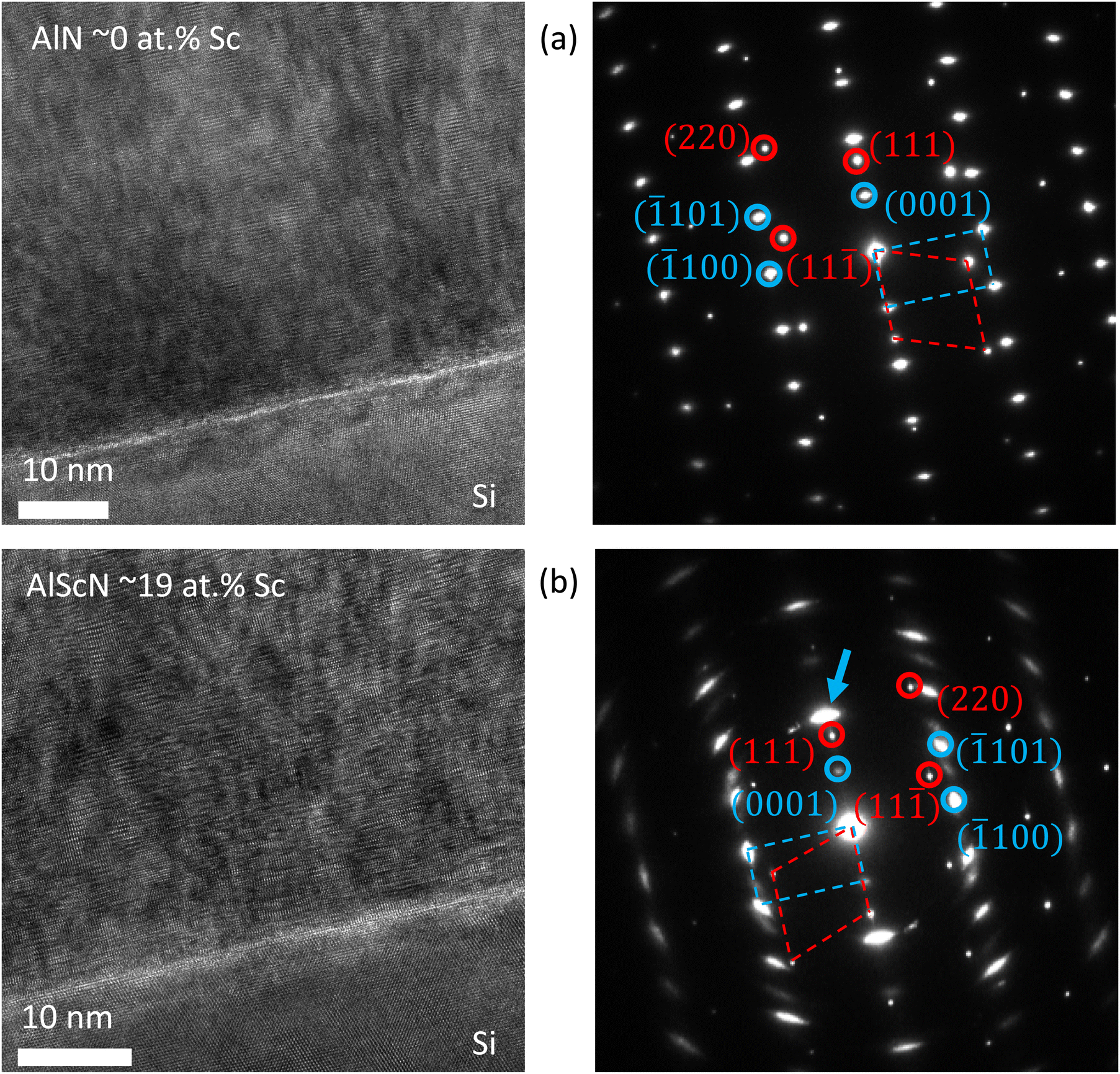 | ||
| Fig. 3 TEM and SAED characterization results: (a) cross section phase contrast image (left) and associated SAED pattern (right) of the AlN film. The SAED shows a superposition of Si [10] and wurtzite [20] zone axis patterns; (b) cross section phase contrast image (left) and associated SAED pattern (right) of the Al0.81Sc0.19N film. The SAED shows a superposition of Si [10] and wurtzite [110] zone axis patterns. Indexing of diffraction spots and one unit cell of the reciprocal space net for Si and wurtzite are shown respectively in red and blue. The blue arrow in (b) highlights the wurtzite (0002) diffraction spot, indicating a significantly increased film mosaic spread when Sc is incorporated into AlN. | ||
At higher Sc concentrations, 31 at% and 37 at%, intensities of the AlScN film diffraction spots are further decreased as compared to those of the Si substrate. While phase contrast images from the Al0.69Sc0.31N film [Fig. 4(a)] and the Al0.63Sc0.37N film [Fig. 4(b)] continue to show lattice fringes with orientation correlation with the Si (111) substrate, the SAED patterns obtained from these two films exhibit a number of common features. First, film diffraction intensities at the reciprocal space location corresponding to wurtzite (0002) indicate substantially higher film mosaic spreads as compared to that for Al0.81Sc0.19N, shown in Fig. 3(b). Second, the wurtzite (0001) double diffraction spot is conspicuously missing in SAED patterns for Al0.69Sc0.31N and Al0.63Sc0.37N. Third, film diffraction intensities are observed at reciprocal space locations that are consistent with both a wurtzite structure and a rocksalt structure, as shown by the schematic reciprocal space nets drawn respectively in green and blue [Fig. 4(a and b)]. Reported bulk lattice constants for the wurtzite AlN are a = 0.311 nm and c = 0.498 nm,29 and reported bulk lattice constant for rocksalt ScN is 0.450 nm.30 The bulk lattice spacing d(0002) of the wurtzitic AlN is 0.249 nm, and the bulk lattice spacing d(111) of the rocksalt ScN is 0.259 nm. When Al is added to rocksalt ScN, the lattice constant decreases,31,32 and when Sc is added to wurtzite AlN, the c lattice constant increases as shown in the present XRD data, making wurtzite d(0002) and rocksalt d(111) values even closer. When the Sc concentration exceeds 30 at%, there is coexistence of both the wurtzite and rocksalt phases as shown by the electron diffraction intensity distributions. However, localizing the different crystal structures spatially in the HRTEM images is not always possible due to complications in the phase contrast arising from large mosaic spread.
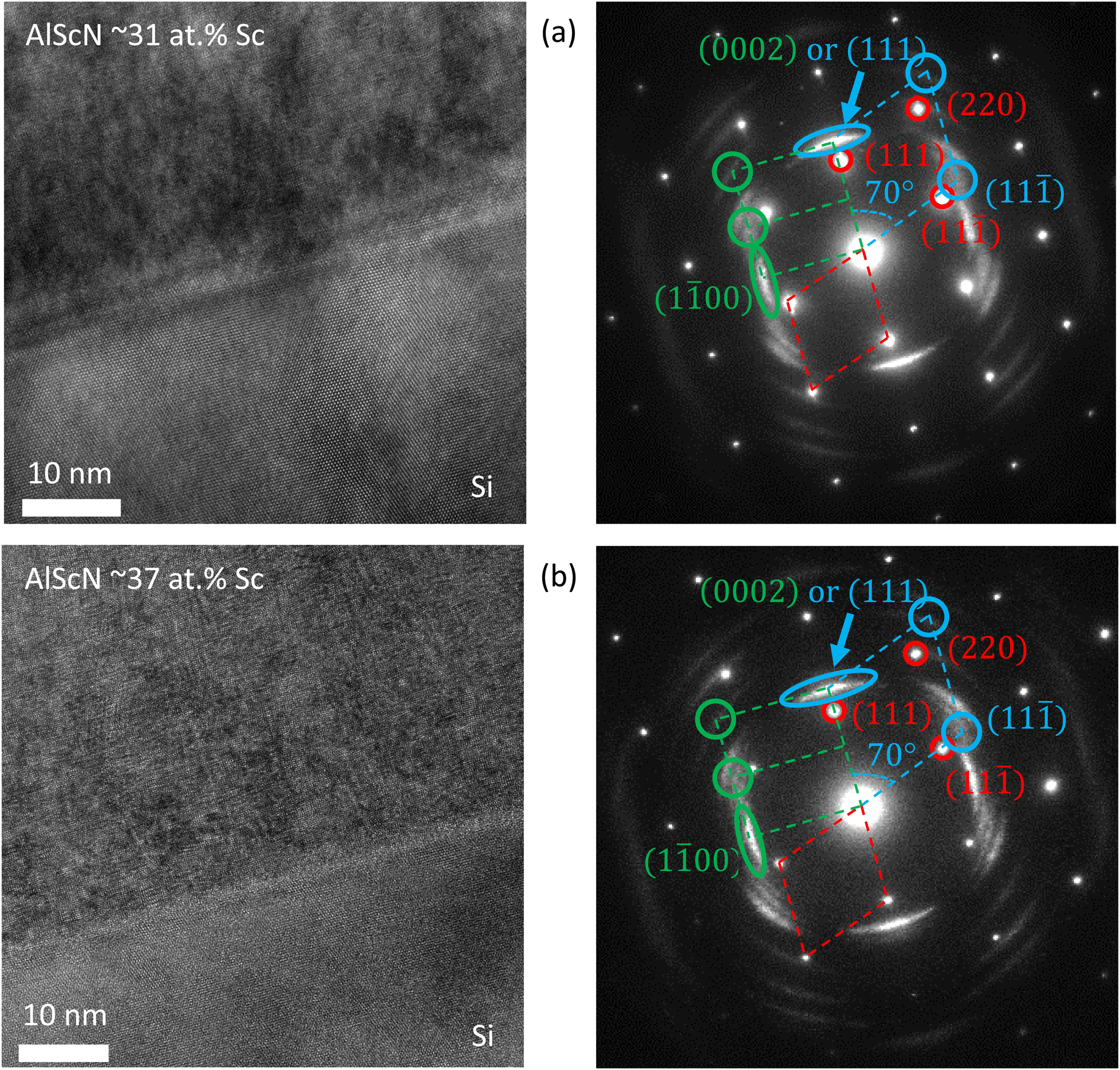 | ||
| Fig. 4 TEM and SAED characterization results: cross section phase contrast image (left) and associated SAED pattern (right) obtained from (a) the Al0.69Sc0.31N film; (b) the Al0.63Sc0.37N film. In the SAED patterns, indexing of Si diffraction spots and reciprocal space net is shown in red; indexing of film diffraction intensities consistent with that from a rocksalt structure and the associated reciprocal space net are shown in blue; and indexing of film diffraction intensities consistent with that from a wurtzite structure and the associated reciprocal space net are shown in green. The blue arrows highlight the (0002)/(111) diffraction spots, showing very large film mosaic spreads. | ||
STEM-EDS maps of AlN and AlScN films are shown in Fig. 5. The STEM high angle annular dark field (HAADF) images all show columnar lamella, which are most pronounced in the 19 at% Sc sample [Fig. 5(b)]. Because the primary mechanism of contrast in these images arises from mass-thickness/atomic number, these images are consistent with compositional segregation. The EDS maps in Fig. 5(b) show that compositional segregation of Sc and Al occurs into lamellar-like structures with wavelengths ∼10 nm. The N concentration is not completely uniform either. This could be consistent with non-uniform nitrogen vacancy concentration or variations in sample thickness. While STEM image contrast persisted in AlScN with Sc concentrations of 31 at% and 37 at%, no significant Sc or Al compositional segregation is observed in these samples.
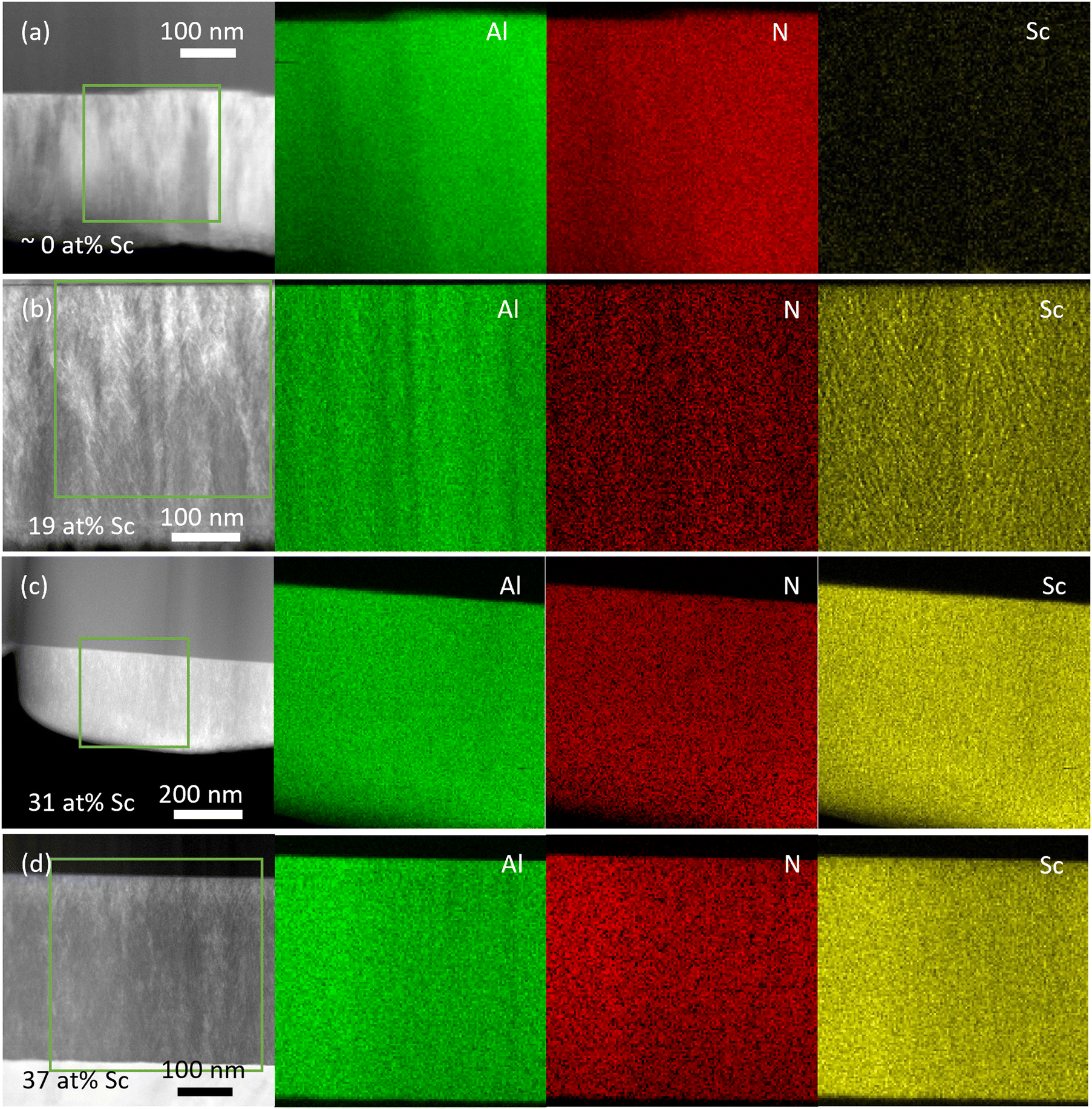 | ||
| Fig. 5 HAADF STEM images and EDS maps of (a) AlN, (b) Al0.81Sc0.19N, (c) Al0.69Sc0.31N, (d) Al0.63Sc0.37N. | ||
In 4D-STEM differential phase contrast mapping33 of the AlN and AlScN films, Fig. 6, the circular color bar is a representation of the ferroelectric polarization vector in polar coordinates, with intensity indicating the magnitude and color indicating the angle/orientation. The images show that domains arise in the material, consistent with nonzero polarization of the material (Fig. 6). In AlN, the differential phase contrast shows domains that are wide and column shaped. The column shaped contrasts are coincident with contrast observed in the STEM images. Differential phase contrast in the 19 at% Sc sample matches the lamellar structure observed in the STEM-EDS maps and HAADF-STEM images. The 31 at% Sc sample also exhibits domains showing variations in the beam displacement. Such domain variations, however, are decreased as compared to those in the 19 at% Sc sample. Finally, the 37 at% Sc sample shows significantly lower magnitude in variation of polarization in the AlScN film region, and the variation occurs on a significantly shorter length scale. We note that the 37 at% Sc sample includes the polycrystalline metal top electrode, which shows differential phase contrast that arises from differences in crystallographic orientation. Because the center-of-mass method is used, relative changes in diffraction intensity that result in shifting of the center of mass of the diffraction pattern also result in differential phase contrast.
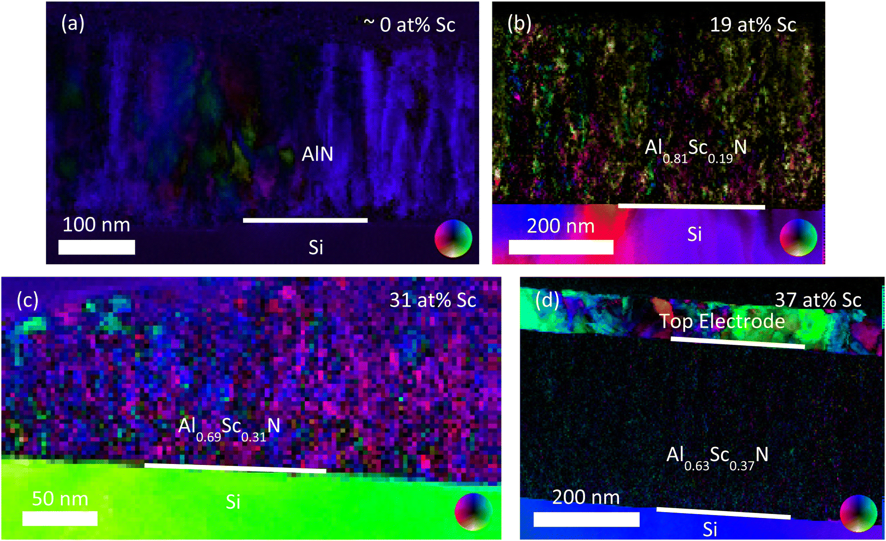 | ||
| Fig. 6 4D-STEM differential phase contrast mapping of: (a) AlN; (b) Al0.81Sc0.19N; (c) Al0.69Sc0.31N; (d) Al0.63Sc0.37N. | ||
To further examine the interface between the nitride films and the Si (111) substrate, high resolution STEM imaging was performed on the AlN and Al0.81Sc0.19N samples. Fig. 7(a) shows a STEM HAADF image of the interface between AlN and Si (111), with the specimen oriented along the Si [10] zone axis direction. The lattice fringes in the Si region show separation between Si atomic columns, indicating that the image resolution is <136 pm. The interface appears diffuse and disordered. Atomic columns at the interface appear blurred. The nitride films appear to have significant mosaic spreads, as the lattice fringes show significant tilt. The contrast in the STEM HAADF image appears to be inverted with respect to expectations, as Al and N are lighter than Si and Z-contrast is the main contrast mechanism in STEM. Similar image features are observed around the interface between Al0.81Sc0.19N and Si (111). In Fig. 7(b), the Si substrate lattice fringes also show clear separation between atomic columns, indicating an image resolution of <136 pm. There are several hemispherical shapes with blurred atomic columns at the interface between AlScN and Si, indicating that this interface is also diffuse. Similar to the AlN sample, the AlScN lattice fringes are also consistent with significant mosaic spread. However, as Sc is significantly heavier than Si, the contrast could be consistent with that expected from Z-contrast.
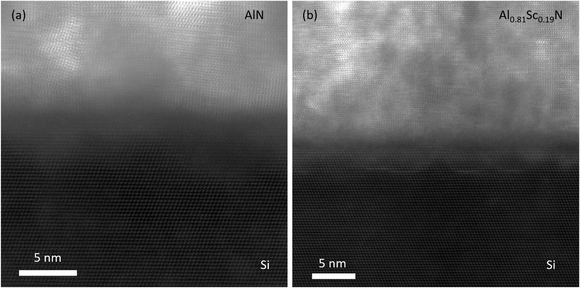 | ||
| Fig. 7 Aberration corrected STEM HAADF images of: (a) AlN; (b) Al0.81Sc0.19N. The electron beam is along the Si [10] zone axis direction. | ||
4. Discussion
While epitaxial growth of AlN on Si (111) substrates is well known, the effect of Sc alloying holds significant interest from an application standpoint. AlScN has been known to adopt the metastable rocksalt structure when grown epitaxially on TiN buffer layers on MgO substrates.31,32 This suggests that the free energy difference between the wurtzite and rocksalt structures is small, and that growth kinetics may play an important role in structure selection. While the XRD results show that the AlN and AlScN films exhibit both out-of-plane and in-plane registry with the Si (111) substrate, the present collection of data confirms the role of Sc alloying on mosaic spread in AlScN and provides context for the concurrent observation of compositional segregation in AlScN. First, the intensity of the film diffraction peaks falls dramatically as the Sc concentration increases. Second, the rocking curve width increase due to Sc alloying is large. This shows that the mosaic spread in the film increases significantly as the Sc concentration increases, and Sc alloying significantly increases disorder in the as-grown film.While the HRTEM imaging does not show clear differences in the AlN and AlScN films, contrast in the images arising from mosaic boundaries is similar to other reports of sputtered AlScN,34,35 and the SAED data are consistent with the differences observed from the XRD data. Electron diffraction features from the AlN film grown on Si (111) are spot-like, whereas diffraction features from the AlScN film are arc-like, with the width of the arc increasing as the Sc concentration increases. This is consistent with the observed increase in ω rocking curve width with increasing Sc concentration. SAED shows that AlN and Al0.81Sc0.19N both adopt the wurtzite crystal structure. The higher Sc concentration AlScN films (31 at% and 37 at% Sc) exhibit sufficient disorder that the (0001) wurtzite reflection is no longer present in the electron diffraction pattern. Film diffraction intensities appear at reciprocal space locations corresponding to wurtzite (100) and rocksalt (11) spots [Fig. 4(a and b)]. The large extent of these arc-shaped spots in reciprocal space is consistent with significant misorientation of the crystal in real space. At the Sc concentrations of 31 at% and 37 at% Sc, the increased disorder and altered diffraction intensity distribution in reciprocal space are consistent with the onset of a wurtzite to rocksalt structure transition. Sputtered polycrystalline AlScN films have been reported to be wurtzite at concentrations as high as 43 at%,1 while epitaxial AlScN films have been reported to be wurtzitic at Sc concentrations up to 41 at%.25 The present results indicate that, for high temperature reactive sputtering, while the wurtzite structure is retained in AlScN films up to ∼20 at% Sc, a disordered and structurally confused wurtzite structure is observed starting at ∼31 at% Sc, indicating the onset of a wurtzite to rocksalt structure transition. The discrepancy between the present results and previous reports may be due to the high temperature used in the present growths, which maintains the system closer to equilibrium as compared to the lower temperatures used in previous studies to sputter polycrystalline films. It is also noted that the lattice mismatch involved in AlN growth on Si (111) is large, ∼23%. Pseudomorphic forces involved in epitaxial growth may be another reason for the discrepancy noted above.
The XRD data hints at the existence of compositional segregation in the AlScN samples. The shape of the (0002) AlScN peak deviates significantly from the symmetric shape of the AlN (0002) peak [Fig. 1(c)], with significant intensity shoulders observed on the higher/lower 2θ sides away from the peak. The asymmetric peak and the intensity shoulders indicate that the (0002) lattice plane spacing is no longer uniform, and the film contains different portions with larger and smaller lattice constants, i.e., higher and lower Sc concentrations. The STEM-EDS mapping results, Fig. 5(b), are thus consistent with the XRD data. The observation that only the AlScN film with the intermediate Sc concentration of 19 at% exhibits lamellar compositional segregation is consistent with spinodal decomposition. In a material system with a positive heat of mixing, the Gibbs free energy as a function of composition at some temperatures can become convex for some intermediate subset of compositions. If a film has a uniform composition within the region in which G is convex, any compositional fluctuation will reduce the overall Gibbs free energy. On the other hand, composition fluctuations outside this region do not exhibit this behavior. For models only considering configurational entropy such as the regular solution model, this means that compositional segregation that occurs at lower compositions and disappears for higher compositions could be consistent with spinodal decomposition. Although there is a report of spinodal decomposition in the AlScN material system,27 the composition at which phase separation is observed is significantly lower in the present work. The higher growth temperatures required for epitaxial growth likely result in more favorable kinetics for the compositional segregation; alternatively, epitaxial misfit strain induced by the substrate could play a role. It is interesting to note that this type of compositional segregation was not reported in either polycrystalline films grown at low temperatures by sputtering,36 or epitaxial films grown at high temperatures by MBE.21 One possibility is that the epitaxial misfit strain at the AlScN/Si interface acts as a driving force for spinodal decomposition, as strain-driven spinodal decomposition is known in ferroelectric and ferroelastic materials.37,38 Furthermore, the lamellar compositional fluctuations coincide with differential phase contrast maps obtained using 4D-STEM. Because 4D-STEM differential phase contrast mapping provides information on electric fields and therefore ferroelectric polarization of the material,39 this suggests that the polarization domains in AlScN are affected by compositional fluctuations. Because previous reports have suggested benefits to device properties such as dielectric breakdown from adopting superlattice structures with composition variations,8 the possibility of leveraging spinodal driven compositional segregation provides an alternate avenue through which self-assembled compositional modulation in epitaxial AlScN thin films can be achieved.
Epitaxial single crystal thin films of AlScN are promising because they provide a materials platform to systematically investigate the structure–property relationship of wurtzitic ferroelectrics/piezoelectrics, which include not only AlN based alloys (AlBN, AlScN), but also ZnO based alloys.40 This approach paves the way for a structure-based approach to understanding device property challenges such as electrical leakage and reliability. The present work clearly demonstrates that reactive sputtered AlScN films on Si (111) are epitaxial. Structural characterization shows that there are a number of challenges in this material system that arise from different levels of disorder. First, the large epitaxial mismatch between AlN (and AlScN) with Si, ∼23% for AlN grown on Si (111), lead to a significant mosaic spread. As a result, while AlScN films maintain both in-plane and out-of-plane registry with the Si (111) substrate, there are mosaic boundaries that appear very similar to low-angle tilt boundaries due to slight misorientations between neighboring mosaic domains. The significant number of dislocations that result could contribute to the observed contrast reversal in the STEM HAADF image of AlN [Fig. 7(a)].41 While it is unknown what the effects of these mosaic boundaries are on the electrical properties of the material, this can in principle be studied by minimizing these types of boundaries through growth of a suitable buffer layer. Second, composition fluctuations resulting from spinodal decomposition add another layer to order and disorder in the material system. While previous reports suggest that compositional segregation may benefit device performance, they also emphasize the importance of controlling structural/compositional variations that can influence optoelectronic device properties. Finally, the structure transition between wurtzite and rocksalt in AlScN offers another degree of freedom in tuning physical properties, details of which remain to be clarified in the future.
5. Conclusion
Epitaxial AlScN thin films on Si (111) were successfully grown using UHV reactive sputtering. The AlScN films form an ideal model system for investigation of wurtzite-based ferroelectrics/piezoelectrics: crystal growth occurs on a facile substrate, and better control over structural parameters influencing electrical properties is achieved through epitaxy. AlScN is observed in the wurtzite structure up to ∼20 at% Sc. Significant structural disorder develops at higher Sc content, >30 at% Sc, coincident with the onset of a wurtzite to rocksalt structure transition. Furthermore, we observe that the high temperature used for epitaxial growth leads to spinodal decomposition even at ∼20 at% Sc, which has not been previously reported. This provides a means for self-assembled compositional segregation in AlScN. 4D-STEM measurements show that polarization domains coincide with the spinodal lamella, suggesting that device behaviors associated with compositional fluctuations could have a structural origin.Conflicts of interest
There are no conflicts to declare.Acknowledgements
XZ and WJM acknowledge partial project support from NSF EPSCoR program under awards OIA-1541079 and OIA-1946231 and use of experimental facilities at the LSU Shared Instrumentation Facility (SIF), a part of the Louisiana Core User Facilities (CUF). This work was carried out in part at the University of Pennsylvania Singh Center for Nanotechnology, which is supported by the NSF National Nanotechnology Coordinated Infrastructure Program under grant NNCI-1542153. The authors gratefully acknowledge use of facilities and instrumentation supported by NSF through the University of Pennsylvania Materials Research Science and Engineering Center (MRSEC) (DMR-1720530).References
- S. Fichtner, N. Wolff, F. Lofink, L. Kienle and B. Wagner, J. Appl. Phys., 2019, 125, 114103 CrossRef.
- J. Hayden, M. D. Hossain, Y. Xiong, K. Ferri, W. Zhu, M. V. Imperatore, N. Giebink, S. Trolier-McKinstry, I. Dabo and J.-P. Maria, Phys. Rev. Mater., 2021, 5, 044412 CrossRef CAS.
- G.-S. Chung and B.-C. Lee, J. Intell. Mater. Syst. Struct., 2014, 26, 1971–1979 CrossRef.
- J. C. Doll, B. C. Petzold, B. Ninan, R. Mullapudi and B. L. Pruitt, J. Micromech. Microeng., 2009, 20, 025008 CrossRef PubMed.
- C. Xiong, W. H. P. Pernice and H. X. Tang, Nano Lett., 2012, 12, 3562–3568 CrossRef CAS PubMed.
- U. C. Kaletta, C. Wipf, M. Fraschke, D. Wolansky, M. A. Schubert, T. Schroeder and C. Wenger, IEEE Trans. Electron Devices, 2015, 62, 764–768 CAS.
- J. Kataoka, S.-L. Tsai, T. Hoshii, H. Wakabayashi, K. Tsutsui and K. Kakushima, Jpn. J. Appl. Phys., 2021, 60, 030907 CrossRef CAS.
- J. X. Zheng, D. Wang, P. Musavigharavi, M. M. A. Fiagbenu, D. Jariwala, E. A. Stach and R. H. Olsson, J. Appl. Phys., 2021, 130, 144101 CrossRef CAS.
- X. Liu, J. Zheng, D. Wang, P. Musavigharavi, E. A. Stach, R. Olsson and D. Jariwala, Appl. Phys. Lett., 2021, 118, 202901 CrossRef CAS.
- D. Wang, P. Musavigharavi, J. Zheng, G. Esteves, X. Liu, M. M. A. Fiagbenu, E. A. Stach, D. Jariwala and R. H. Olsson, Phys. Status Solidi RRL, 2021, 15, 2000575 CrossRef CAS.
- M. Pirro, G. Giribaldi, B. H. Soukup, X. Zhao, G. Michetti, W. Zhu, L. Colombo, C. Cassella and M. Rinaldi, 2021 Joint Conference of the European Frequency and Time Forum and IEEE International Frequency Control Symposium (EFTF/IFCS), Gainesville, FL, 2021, DOI:10.1109/EFTF/IFCS52194.2021.9604316.
- R. Nie, S. Shao, Z. Luo, X. Kang and T. Wu, Micromachines, 2022, 13, 1629 CrossRef PubMed.
- E. Österlund, G. Ross, M. A. Caro, M. Paulasto-Kröckel, A. Hollmann, M. Klaus, M. Meixner, C. Genzel, P. Koppinen, T. Pensala, A. Žukauskaitė and M. Trebala, Phys. Rev. Mater., 2021, 5, 035001 CrossRef.
- C. S. Sandu, F. Parsapour, S. Mertin, V. Pashchenko, R. Matloub, T. LaGrange, B. Heinz and P. Muralt, Phys. Status Solidi A, 2019, 216, 1800569 CrossRef.
- R. Beaucejour, V. Roebisch, A. Kochhar, C. G. Moe, M. D. Hodge and R. H. Olsson, J. Microelectromech. Syst., 2022, 31, 604–611 CAS.
- W. Lin, W. Cheng, Y. Wang, Y. Sun, Q. Zha, C. Zeng, Q. Cui and B. Zhang, 2021 5th IEEE Electron Devices Technology & Manufacturing Conference (EDTM), Chengdu, China, 2021 DOI:10.1109/EDTM50988.2021.9421009.
- W. J. Meng, J. Heremans and Y. T. Cheng, Appl. Phys. Lett., 1991, 59, 2097–2099 CrossRef CAS.
- M. Morita, S. Isogai, N. Shimizu, K. Tsubouchi and N. Mikoshiba, Jpn. J. Appl. Phys., 1981, 20, L173 CrossRef CAS.
- M. Miyauchi, Y. I. Yukari Ishikawa and N. S. Noriyoshi Shibata, Jpn. J. Appl. Phys., 1992, 31, L1714 CrossRef CAS.
- C. Manz, S. Leone, L. Kirste, J. Ligl, K. Frei, T. Fuchs, M. Prescher, P. Waltereit, M. A. Verheijen, A. Graff, M. Simon-Najasek, F. Altmann, M. Fiederle and O. Ambacher, Semicond. Sci. Technol., 2021, 36, 034003 CrossRef CAS.
- D. Wang, P. Wang, S. Mondal, Y. Xiao, M. Hu and Z. Mi, Appl. Phys. Lett., 2022, 121, 042108 CrossRef CAS.
- S. Leone, J. Ligl, C. Manz, L. Kirste, T. Fuchs, H. Menner, M. Prescher, J. Wiegert, A. Žukauskaitė, R. Quay and O. Ambacher, Phys. Status Solidi RRL, 2020, 14, 1900535 CrossRef CAS.
- G. Wingqvist, F. Tasnádi, A. Žukauskaitė, J. Birch, H. Arwin and L. Hultman, Appl. Phys. Lett., 2010, 97, 112902 CrossRef.
- N. Wolff, S. Fichtner, B. Haas, M. R. Islam, F. Niekiel, M. Kessel, O. Ambacher, C. Koch, B. Wagner, F. Lofink and L. Kienle, J. Appl. Phys., 2021, 129, 034103 CrossRef CAS.
- Y. Lu, M. Reusch, N. Kurz, A. Ding, T. Christoph, M. Prescher, L. Kirste, O. Ambacher and A. Žukauskaitė, APL Mater., 2018, 6, 076105 CrossRef.
- B. Sundarapandian, M. Kessel, A. Žukauskaitė, L. Kirste, C. Sun and O. Ambacher, 2020 IEEE International Ultrasonics Symposium (IUS), Las Vegas, NV, 2020 DOI:10.1109/IUS46767.2020.9251791.
- K. R. Talley, S. L. Millican, J. Mangum, S. Siol, C. B. Musgrave, B. Gorman, A. M. Holder, A. Zakutayev and G. L. Brennecka, Phys. Rev. Mater., 2018, 2, 063802 CrossRef CAS.
- B. Alling, A. Karimi and I. A. Abrikosov, Surf. Coat. Technol., 2008, 203, 883–886 CrossRef CAS.
- S. Iwama, K. Hayakawa and T. Arizumi, J. Cryst. Growth, 1982, 56, 265–269 CrossRef CAS.
- W. Lengauer, J. Solid State Chem., 1988, 76, 412–415 CrossRef CAS.
- B. Saha, G. V. Naik, S. Saber, C. Akatay, E. A. Stach, V. M. Shalaev, A. Boltasseva and T. D. Sands, Phys. Rev. B: Condens. Matter Mater. Phys., 2014, 90, 125420 CrossRef.
- B. Saha, S. Saber, G. V. Naik, A. Boltasseva, E. A. Stach, E. P. Kvam and T. D. Sands, Phys. Status Solidi B, 2015, 252, 251–259 CrossRef CAS.
- C. Ophus, Microsc. Microanal., 2019, 25, 563–582 CrossRef CAS PubMed.
- C. Höglund, B. Alling, J. Birch, M. Beckers, P. O. Å. Persson, C. Baehtz, Z. Czigány, J. Jensen and L. Hultman, Phys. Rev. B: Condens. Matter Mater. Phys., 2010, 81, 224101 CrossRef.
- C. Höglund, J. Birch, B. Alling, J. Bareño, Z. Czigány, P. O. Å. Persson, G. Wingqvist, A. Žukauskaitė and L. Hultman, J. Appl. Phys., 2010, 107, 123515 CrossRef.
- P. Musavigharavi, A. C. Meng, D. Wang, J. Zheng, A. C. Foucher, R. H. Olsson and E. A. Stach, J. Phys. Chem. C, 2021, 125, 14394–14400 CrossRef CAS.
- F. Xue, Y. Ji and L.-Q. Chen, Acta Mater., 2017, 133, 147–159 CrossRef CAS.
- J. W. Cahn, Acta Metall., 1961, 9, 795–801 CrossRef CAS.
- J. A. Hachtel, J. C. Idrobo and M. Chi, Adv. Struct. Chem. Imaging, 2018, 4, 10 CrossRef PubMed.
- K. Ferri, S. Bachu, W. Zhu, M. Imperatore, J. Hayden, N. Alem, N. Giebink, S. Trolier-McKinstry and J.-P. Maria, J. Appl. Phys., 2021, 130, 044101 CrossRef CAS.
- J. Tessmer, S. Singh, Y. Gu, J. A. El-Awady and M. D. Graef, Ultramicroscopy, 2020, 219, 113124 CrossRef CAS PubMed.
| This journal is © The Royal Society of Chemistry 2023 |