
Evaluating charge-type of polyelectrolyte as dielectric layer in memristor and synapse emulation†
Jingzhou
Shi
b,
Shaohui
Kang
b,
Jiang
Feng
a,
Jiaming
Fan
b,
Song
Xue
a,
Gangri
Cai
 *a and
Jin Shi
Zhao
*b
*a and
Jin Shi
Zhao
*b
aTianjin Key Laboratory of Organic Solar Cells and Photochemical Conversion, Department of Applied Chemistry, Tianjin University of Technology, No. 391, Binshui Xidao, Xiqing District, Tianjin, 300384, PR China. E-mail: caigangri@sina.com
bTianjin Key Laboratory of Film Electronic & Communication Devices, School of Integrated Circuit Science and Engineering, Tianjin University of Technology, No. 391, Binshui Xidao, Xiqing District, Tianjin, 300384, PR China. E-mail: jinshi58@163.com
First published on 30th January 2023
Abstract
Based on credible advantages, organic materials have received more and more attention in memristor and synapse emulation. In particular, an implementation of the ionic pathway as a dielectric layer is essential for organic materials used as building blocks of memristor and artificial synaptic devices. Herein, we describe an evaluation of the use of positive and negative polyelectrolytes as dielectric layers for a memristor with calcium ion (Ca2+) doping. The device based on a negative polyelectrolyte shows the potential to obtain an excellent resistive switching performance and synapse functionality, especially in the transformation behaviours from short-term plasticity (STP) to long-term plasticity (LTP) in both the potentiation and depression processes, which were comparable to the perfomrmance obtained with a positive polyelectrolyte. The mechanism of electrical resistance transition and synaptic function can be attributed to the migration of the doped Ca2+ and the ionic functional groups of polyelectrolyte, which result in the formation and vanishing filament-like Ca2+ flux.
New conceptsAn implementation of an ionic pathway as a dielectric layer is essential when using organic materials as building blocks for memristor and artificial synaptic devices, where the diffusion of metal ions such as Ag+, alkali and alkaline metal ions are used to mimic the diffusion of calcium ions (Ca2+) in the neural cell. In this work, polyelectrolytes, as a water-tolerant material, and a solid polymer electrolyte, were straightforward to use as a dielectric layer in a memristor with calcium ion doping, where the current is carried by the calcium ion migration in the polyelectrolyte layers. Moreover, the charge-types of the polyelectrolytes were evaluated as a dielectric layer, which was critical factor for the construction of a calcium ion flux. The negative polyelectrolyte-based device, which is simply prepared by spin-coating a negative polyelectrolyte with Ca2+ on an ITO substrate followed by a magnetron sputtered ITO as top electrode, shows highly promising memory properties, as well as synapse functionality. It shows that the formation of Ca2+ flux is restricted by the same charge-type in the organic dielectric layer, and facilitated by the opposite charge matrix in the organic dielectric layers. This work provides a feasible strategy for the use of a polyelectrolyte as dielectric layer in memristors and artificial synapses. |
Introduction
In 1962, a resistance switching (RS) device was reported by Hickmott, which prompted the investigation and gradual commercialisation of Resistive Random Access Memory (RRAM),1 and it was one of the most promising nanoscale memristor devices.2–4 The basic structure of the RRAM is two layers of conductive electrode material with a layer of semiconducting or insulating dielectric material between them as a functional layer. During the last decade, a number of materials have been investigated for use the functional layer of the RRAM, including inorganic oxides, two-dimensional materials, polymers, and various molecular systems.5–10 Among the materials, the organic materials have attracted a great amount of attention due to their wide variety, low cost, simple fabrication process, good flexibility and so on.8–14Generally, organic materials are used as redox materials for active layers9–12 or ionic/atomic pathway materials for dielectric layers.13,14 Gregor first achieved the resistance switching effect using the organic material, poly(divinylbenzene), which appeared to be related to the conjugated electronic structure of the monomer.11 Goswami et al. reported a resistive memory device based on a spin-coated active layer of a transition-metal complex with an azo-aromatic ligand which was used for redox processes for performing memory effects.12 Moreover, a memristor using organic materials as a dielectric layer proved to be superior for artificial neural computing, where the diffusion of the metal ions such as Ag+, Cu+, alkali and alkaline metal ions are used to mimic the diffusion of Ca2+ in the neural cell. Chen et al. presented an RRAM device fabricated by spin-coating a chicken egg albumen layer, which showed a low operating voltage and high stability.13 Raeis-Hosseini et al. reported collagen extracted from fish skin used as an active layer in a neuromorphic device.14 The simple artificial synaptic device with a structure of Mg/collagen/ITO showed a reliable neuromorphic functionality based on Mg ion migration in collagen film. Thus, organic materials can undertake a role as a pathway for the metal ion migration in memory devices. However, understanding the memristor and finding suitable renewable materials for it and the artificial synapse devices are still a challenge for industrialising organic materials.
Polyelectrolytes, have used been as water-tolerant materials in many applications, such as diodes, transistors, photovoltaic devices and memristors, where the current is carried by ions.15–21 It is not only a natural insulation material, but also an ionic conducting material which is superior for use as an ionic pathway for a dielectric layer.22,23 Xu and Wang reported water-soluble conjugated polyelectrolyte-based memristors and synapses.20,21 However, there is scope to improve the performance of memristors and synapses, and for a greater understanding of the working principle. In this research, we evaluated the use of positive (poly(ethyleneimine), PEI) and negative (poly(acrylic acid), PAA) polyelectrolytes as the ionic pathway layer in a memristor device with Ca2+ doping (ITO/PEI-Ca2+/ITO and ITO/PAA-Ca2+/ITO), which was simple to prepare by spin-coating the PEI or PAA solution with Ca2+ on to the ITO substrate followed by magnetron sputtering of the ITO as the top electrode (TE). This showed that the memory performance of the polyelectrolyte-based devices was clearly dependent on the charge-type of the polyelectrolyte. The device based on a negative polyelectrolyte (PAA) shows the potential to obtain an excellent memory performance and synapse functionality, which is comparable to the device based on the positive charge polyelectrolyte (PEI). The mechanism of electrical resistance transition and synaptic function can be attributed to the formation of an ion flux and showed an ion depleted layer in the polyelectrolyte dielectric layers.
Results and discussion
Preparation and RS property of polyelectrolyte-based devices
Transparent ITO/PEI-Ca2+/ITO and ITO/PAA-Ca2+/ITO devices were prepared by spin-coating aqueous solutions of PEI and PAA with Ca2+ ions on to a ITO glass substrate (as shown in Fig. 1a), and Fig. 1b shows the molecular structures of PAA and PEI. Fig. 1c shows the transmittance measurements of polyelectrolyte-based devices, which exhibited optical transmittance of more than 85%. Atomic force microscopy (AFM) was carried out to monitor film deposition, as shown in Fig. 1d (bare ITO surface). Fig. 1e (PEI-Ca2+/ITO surface), and Fig. 1f (PAA-Ca2+/ITO surface), show that the polyelectrolyte with a Ca2+ thin film was successfully deposited onto the ITO substrates (for comparison, the AFM topographic images of the films without Ca2+ are shown in Fig. S1, ESI†). The thicknesses of the PEI-Ca2+ and PAA-Ca2+ films were ∼25 nm and ∼20 nm, respectively, which were measured using cross-sectional SEM images as shown in Fig. S2 (ESI†). Moreover, XPS was performed for determining the amount of calcium (at%) of the films, as shown in Fig. S3 (ESI†), which was ∼5% for both PEI- and PAA-based films (the details of the atomic percentages are showed in Table S1, ESI†). Then a top ITO electrode was deposited using magnetron sputtering for further standard electrical characterisation.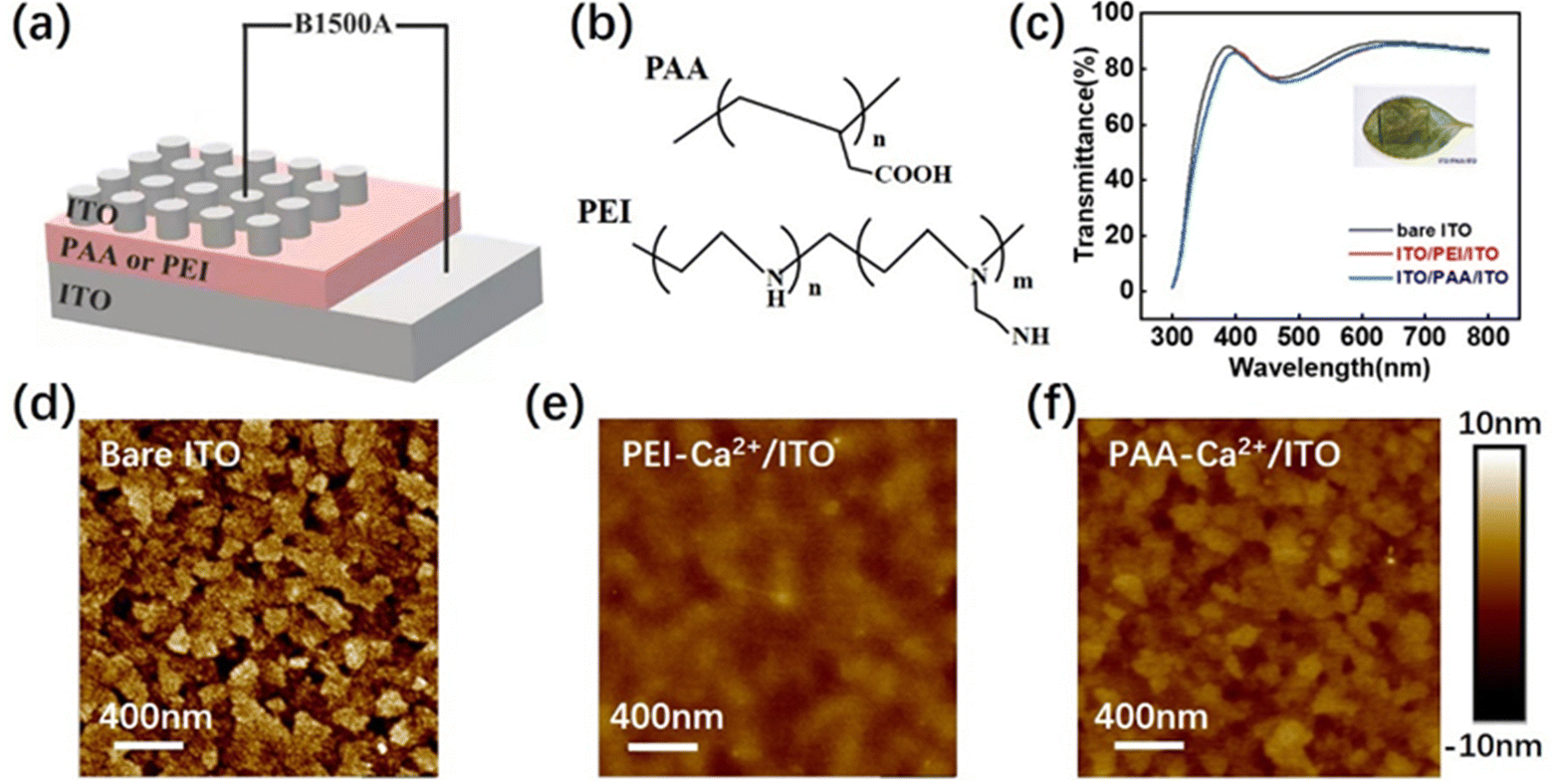 | ||
| Fig. 1 (a) Device structure, (b) molecular structures, and (c) transmittance of a polyelectrolyte-based device; AFM topographic images of (d) bare ITO, (e) PEI-Ca2+/ITO, and (f) PAA-Ca2+/ITO surfaces. | ||
Fig. 2 shows the standard electrical characterisation of polyelectrolyte-based devices. As shown in Fig. 2a and 2b, the devices with PEI as a dielectric layer exhibited poor bipolar resistance switching behaviour even with Ca2+ doping. Notably, the ITO/PEI-Ca2+/ITO device showed a current decrease phenomena with sequential current–voltage (I–V) sweeping. Fig. 2c shows the I–V curves of PAA as dielectric layer without Ca2+ doping, which also shows poor switching behaviour. It was noted that the poor switching behaviour of the devices without Ca2+ doping was realised by indium ion diffusion in the polyelectrolyte dielectric layer (few of the indium atoms were detected in the films by XPS as shown in Table S1, ESI†). In particular, the ITO/PAA-Ca2+/ITO device showed excellent switching behaviour, as shown in Fig. 2d. The set process showed that the current gradually increased from 0 to 0.5 V, when a negative bias was applied to the device, and it also showed an accelerative increment at the voltage of 0.5 to 1.0 V. The subsequent reset process showed that the current quickly decreased from 1.5 to 1.8 V, which was much greater than the voltage of set process. However, the overall I–V characteristics showed a gently changing trend, which provided a favourable basis for the biomimetic synapses. Moreover, the RS reliability was verified by the endurance and retention tests. The 100 I–V sweeps of a PAA-Ca2+ based memory cell are shown in Fig. S4a (ESI†), and a RS ratio of ∼100 times was maintained for more than 5,000 RS cycles (as shown in Fig. S4b, ESI†). In addition, the retention tests were also carried out at room temperature (Fig. S5a, ESI†) and 85 °C (Fig. S5b, ESI†). The PAA-Ca2+ based device maintained a high-resistance state (HRS) and a low resistance state (LRS) for 1 × 10⁴ s at both temperatures, suggesting that it was a stable and non-volatile memory device. Notably, according to the previous results, the charge-type of the polyelectrolyte is a decisive factor for achieving RS behaviour in the Ca2+ doping devices.
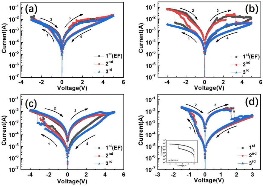 | ||
| Fig. 2 Current–voltage characteristics of (a) ITO/PEI/ITO/glass, (b) ITO/PEI-Ca2+/ITO/glass, (c) ITO/PAA/ITO/glass and (d) ITO/PAA-Ca2+/ITO/glass, where the inset figure displays an electroforming curve in a negative bias region. | ||
Investigation of the working principle
To determine the mechanism, the EDS mapping of the calcium was carried out on the PEI- and PAA-Ca2+ devices (the EDS measurements of the ITO, used as the TE) before and after the setting process. For comparison, the EDS mapping of the indium (In) element was used as standard reference. Fig. 3a and b show the EDS mapping images of calcium from the PAA-Ca2+ based device before and after the setting process, respectively. Before setting, as shown in Fig. 3a, the calcium elements were uniformly dispersed in the PAA film, and these are shown as lots of small dots in the EDS mapping image. After setting, it showed fewer but bigger dots in the calcium EDS mapping image comparing to those before setting, as shown in Fig. 3b. In particular, in the EDS data of both before and after the setting process, the atomic ratios of indium to calcium were similar and were about 40![[thin space (1/6-em)]](https://www.rsc.org/images/entities/char_2009.gif) :1. In the PEI-based devices, there was no significant difference in the EDS mapping images of the before and after setting process, which showed a uniform dispersion of the Ca element (see Fig. S6a and S6b, ESI†). Furthermore, the peak force tunnelling atomic force microscopy (PFTUNA) was performed on PEI- and PAA-Ca2+ devices under identical conditions to the EDS mapping. The PFTUNA image of the device with Ca2+ doping showed an average current of −0.28 pA (see Fig. 3c) before setting, which was lower than that of the device after setting (−1.68 pA) with an applied voltage of −1 V, as shown in Fig. 3d. In particular, there were many obvious local conducting points (shown as dark points) in the PFTUNA image of the PAA-Ca2+ based device after setting, which suggested that the conduction occurred from the local points. Also, there was no significant difference in the PFTUNA images taken before and after the setting process in the PEI-based devices (see Fig. S6c and S6d, ESI†).
:1. In the PEI-based devices, there was no significant difference in the EDS mapping images of the before and after setting process, which showed a uniform dispersion of the Ca element (see Fig. S6a and S6b, ESI†). Furthermore, the peak force tunnelling atomic force microscopy (PFTUNA) was performed on PEI- and PAA-Ca2+ devices under identical conditions to the EDS mapping. The PFTUNA image of the device with Ca2+ doping showed an average current of −0.28 pA (see Fig. 3c) before setting, which was lower than that of the device after setting (−1.68 pA) with an applied voltage of −1 V, as shown in Fig. 3d. In particular, there were many obvious local conducting points (shown as dark points) in the PFTUNA image of the PAA-Ca2+ based device after setting, which suggested that the conduction occurred from the local points. Also, there was no significant difference in the PFTUNA images taken before and after the setting process in the PEI-based devices (see Fig. S6c and S6d, ESI†).
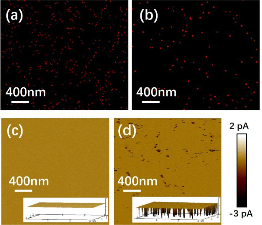 | ||
| Fig. 3 The EDS mapping images of the PAA-Ca2+ memory device: (a) before setting, (b) after setting. The PFTUNA current mapping images of the PAA-Ca2+ memory device (inserts are the 3D images): (c) before setting, (d) after setting. | ||
Furthermore, the Ca2+ doped devices with different thickness of polyelectrolyte films were prepared, to optimise the film thickness and determine the effects of thickness, as shown in Fig. S7, ESI.† With thin polyelectrolyte films (Fig. S7a and S7b, ESI†), the I–V curves of the devices almost overlapped in the voltage sweep cycles, which indicated that the thin PEI (∼8 nm) and PAA (∼5 nm) layers had no RS property (see Fig. S8a and S8b, ESI†). With thick polyelectrolyte films (Fig. S7c and S7d, ESI†), the PEI (∼80 nm) based device showed almost an overlapping I–V curve (see Fig. S8c, ESI†), and the PAA (∼70 nm) based device showed a poor RS property (Fig. S8d, ESI†). It was noted that the thin polyelectrolyte films could not act as the dielectric layer very well, and the doped Ca2+ could initially contact the TE and bottom electrode (BE), resulting in ohmic contact. However, the thick polyelectrolyte layer blocked the electric field to effect the ion migration.
According to the previously mentioned observations, it was noted that the ion migration in the polyelectrolyte layer lead to RS behaviour. As shown in Scheme 1a, in the initial state, the Ca2+ was randomly distributed in the PEI (pristine state) layer. When a negative bias was applied to the TE of the PEI-Ca2+ device, the cations (–NH3+) of PEI (close to ITO electrode surface) firstly moved to the surface of the TE to form a cationic layer, which blocked Ca2+ from contacting the TE (as shown in Scheme 1b). In addition, when a positive bias was applied, identical behaviour was achieved on the surface of the BE, which blocked Ca2+ ions from contacting the electrode (as shown in Scheme 1c). However, the beginning sweep of the PEI-Ca2+ device showed poor RS behaviour because the cationic layer could not completely block the Ca2+ from contacting the electrode, as shown in Fig. 2b. Moreover, the I–V sweeps of the pristine state were compared when determining the blocking behaviours of PEI, as shown in Fig. S9a (ESI†). With an applied negative bias, it showed a similar current between without (black line) and with (red line) Ca2+ doped devices, which implied that the ionised PEI layer on the surface of the electrode blocked the doped Ca2+ to affect the current. Furthermore, with continuous I–V sweeping, the cationic blocking layer would be improved because of the moving rate difference between Ca2+ and –NH3+. When applying a subsequent positive bias, the Ca2+ left from the electrode, and it was faster than the cations (–NH3+) of PEI, and there was more and more –NH3+ found on the electrode surface, resulting in an improvement of the cationic blocking layer. Hence, the current was decreased with continuous I–V sweeps (as shown in Fig. 2b), and there was no robust RS behaviour of the PEI-based devices.
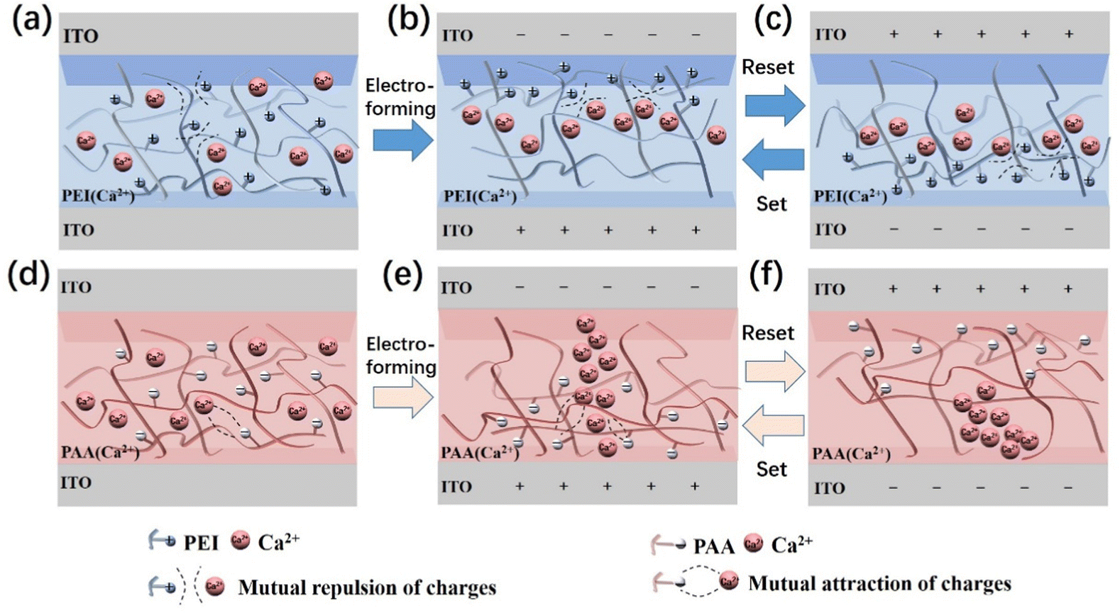 | ||
| Scheme 1 Schematic illustration of the internal structure during electro setting/resetting: (a–c) PEI- and (d–f) PAA-based devices. | ||
In the PAA-based devices, the Ca2+ were also uniformly distributed in the PAA layer initially, as shown in Scheme 1d. When a negative bias was applied to the TE of the PAA-Ca2+ device, because the dielectric layer was a negatively charged polyelectrolyte of PAA, there was no impedance of Ca2+ migration, and the Ca2+ could comfortably contact the electrode surface, resulting in a LRS. Moreover, the I–V sweeps of the pristine state were compared for determining the doping effect of the PAA-based devices, as shown in Fig. S9b (ESI†). When a negative bias was applied to the TE, the device with Ca2+ doping (red line) showed a much higher current than the device without Ca2+ doping (black line), which implied that the PAA did not impede the Ca2+ migration, and the doped Ca2+ affected the current. In particular, according to the results of the EDS mapping and PFTUNA, it was noted that the Ca2+ was centralised into a filament-like ion flux when a negative bias was applied to the TE, as shown in Scheme 1e.24,25 Moreover, the anions (–COO−) of PAA provided a favourable basis of an anionic channel for the construction of a filament-like Ca2+ flux. In the subsequent reset process, which in which a positive bias was applied on the TE, the reset voltage (1.5 V) was higher than the set voltage (−0.5 V) because the Ca2+ needed to be completely expelled from the TE surface, resulting in a Ca-depleted region (HRS), as shown in Scheme 1f. Thus, it was noted that the memristor character of the PAA-based device was achieved by the formation and disappearance of the Ca2+ fluxes (filament-like), which was supported by the anion (–COO−) of the PAA constructed ion channel.
Synaptic plasticity
Furthermore, the PAA-Ca2+ memory device was used to simulate artificial synaptic behaviour. Fig. 4a shows the potentiation/depression behaviours of the sample with slightly different pulse conditions, which was more relevant to artificial neural networks (ANNs).26–28 As 100 negative pulses (−0.7 V, 1 ms) were continuously stimulated, the device current gradually increased, whereas when the 100 positive pulses (0.7 V, 1 ms) were stimulated with the same voltage amplitude, the current decreased continuously, suggesting that the PAA-Ca2+ based device was promising for ANN applications. The application of spiking neural networks (SNNs) using PAA-Ca2+ based memory devices was also performed, as shown in Fig. 4b. The performance of paired-pulse facilitation (PPF) was evaluated using −0.4 V/20 ms pulses, with intervals ranging of 1 ms to 2 s. When a pair of presynaptic pulses (−0.4 V/20 ms) were applied at different pulse intervals, the second pulse (post synapse) produced a higher current than the first. The PPF index was found to obviously dependent on the interval, and was well fitted by the double exponential function.29,30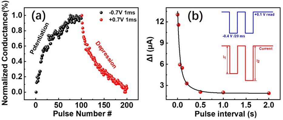 | ||
| Fig. 4 (a) Potentiation/depression in the polyelectrolyte artificial synapse over 100 consecutive voltage pulses, and (b) implementation of PPF. | ||
Furthermore, the behaviour of the excitatory postsynaptic current (EPSC) in the biological synapses using PAA-Ca2+ based devices was also performed, and the results are shown in Fig. 5. The STP of the synaptic behaviour was indicated by the relaxation time required for the current to return to the resting state, which could increase with the decreasing (absolutely increasing) pulse amplitude (−0.3, −0.4, or −0.5 V). When the absolute pulse amplitude increased to −0.5 V, the STP can transition to LTP, as shown in Fig. 5a–c. In particular, the device has also shown its ability to implement short-term and long-term depressions, and controlled transitions between the two, as shown in Fig. 5d–f. It was observed that the positive pulse (0.6 V; 100 ms) started to cause the STD, and the relaxation time of the STD increased with the pulse amplitude. When the positive pulse amplitude reached 0.8 V, the state changed from STD to LTD (Fig. 5f). This study found that both STP and LTP can be realised in both the potentiation and depression processes. This ability is regarded as essential for developing neuromorphic systems with complex cognitive capabilities.31,32 It was noted that the synapse functionalities were also achieved by the construction of filament-like Ca2+ flux. At an low voltage, the slender filament-like Ca2+ flux could be constructed, and it was easy for it to be cracked thermodynamically, and facilitate an interaction between Ca2+, resulting in the STP behaviour. The anionic channel of PAA cannot be constructed using a low voltage. When a high voltage was applied, the robust filament-like Ca2+ flux and anionic channel of PAA were constructed, resulting in LTP behaviour. However, when the robust filament-like Ca2+ flux was constructed, a higher voltage should be applied to crack the filament-like Ca2+ flux, which is the reason that the pulse potential of the depression process is greater than that of the potentiation process. When a low voltage was applied, the robust filament-like Ca2+ flux was cracked locally, and it would be restored by the thermodynamics and diffusion of Ca2+, resulting in STD behaviour. When a higher voltage was applied, the filament-like Ca2+ flux was destroyed, resulting in the LTD behaviour.
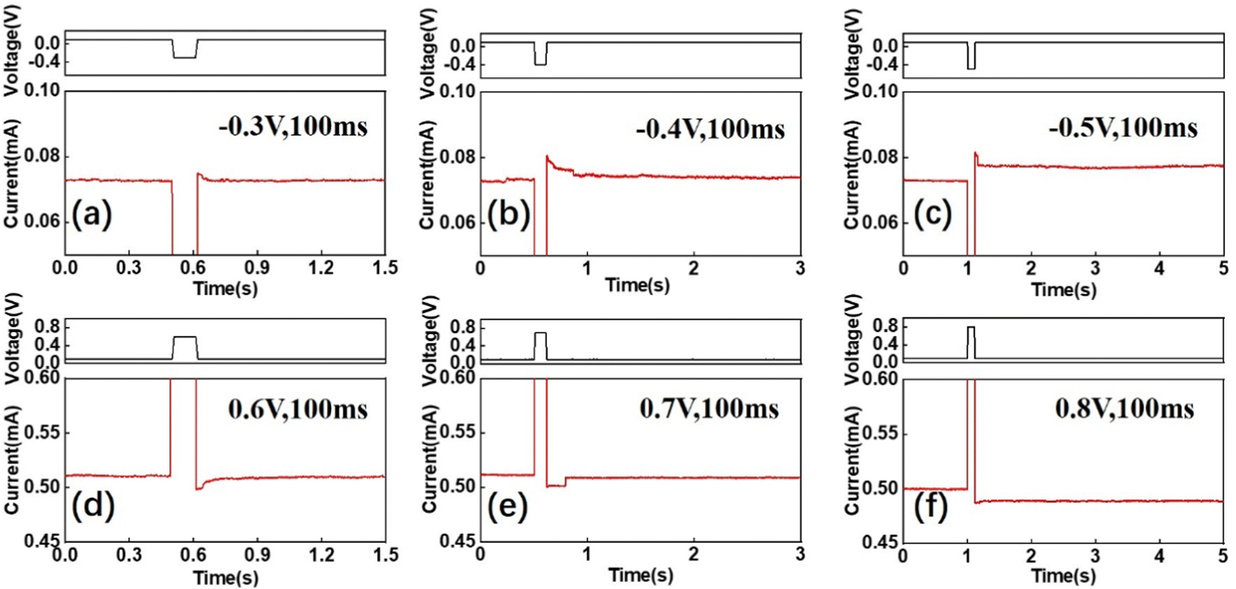 | ||
| Fig. 5 The behaviour of the EPSC in biological synapses with the amplitude of pulses in both potentiation and depression processed, and a low voltage reading of 0.1 V was always applied. (a–c) The device was stimulated by a single positive pulse with a constant width (100 ms) and various amplitudes of −0.3, −0.4 or −0.5 V; (d–f) the device was stimulated by a positive pulse with a constant width (100 ms) and various amplitudes of 0.6, 0.7 or 0.8 V. | ||
Moreover, the pulse number induced synaptic behaviour and was also investigated as shown in Fig. S10 (ESI†). Fig. S10a–S10d (ESI†) show that the transition from STP to LTP, which was realised as the number of pulses increased from 1 to 30 at a specific pulse condition (amplitude = −0.3 V, width = 100 ms, and interval = 20 ms). These behaviours were understood to be the Ca2+ diffusion induced stability of the filament-like Ca2+ flux during the pulse interval.
Conclusions
The positive (PEI) and negative (PAA) polyelectrolytes were evaluated for use as a dielectric layer with calcium ion doping in a memristor. This demonstrated that the charge-type of the dielectric layer is a crucial factor for exhibiting RS behaviour. The positive polyelectrolyte impedes construction of a metal ion flux, and the negative polyelectrolyte supports construction of metal ion flux. The PAA-based device, which is simply prepared by spin-coating a negative polyelectrolyte of PAA with Ca2+ onto an ITO substrate followed by a magnetron sputtered ITO as the TE, shows highly promising memory properties, as well as synapse functionalities. The RS behaviour was achieved by the formation and disappearance of the filament-like Ca2+ flux in a negative charged dielectric layer which provided a favourable basis for the cation flux construction. Moreover, it shows the transformation behaviours from STP to LTP in both the potentiation and depression processes, which is realised by cracking and then restoring the filament-like Ca2+ flux. This study determined that the formation of the positive metal ion flux was restricted by the same charge in the organic dielectric layer, and facilitated by the opposite charge matrix in the organic dielectric layers. This provides valuable practice for the application of a solid polymer electrolyte in a memristor, and demonstrates the feasibility of obtaining highly transparent, flexible and biocompatible synapses for use in artificial intelligence systems.Author contributions
Jingzhou Shi: fabricated the devices, and carried out the laboratory research of FESEM, UV-Vis spectrometry, AFM, I–V characterisation and synapse functionality analysis. Shaohui Kang: fabricated the devices, and carried out the laboratory research of I–V characterisation and synapse functionality analysis. Jiang Feng: carried out I–V characterisation and synapse functionality analysis. Jiaming Fan: carried out I–V characterisation and synapse functionality analysis. Song Xue: provided guidance on the experimental designs, and understanding of the phenomena. Gangri Cai: provided guidance on the experimental designs and understanding of the phenomena, and supervised the entire research programme and writing of the report. Jin Shi Zhao: provided guidance on the experimental designs and understanding of the phenomena, and supervised the entire research programme.Conflicts of interest
There are no conflicts to declare.Acknowledgements
This work is supported by the Innovative Talents Promotion Plan in Tianjin (Grant No. 2020TD003), the Tianjin Technical Expert Project (Grant No. 22YDTPJC00390 and 22YDTPJC00530) and the National Natural Science Foundation of China (Grant No. 62004140 and 22078248).Notes and references
- T. W. Hickmott, J. Appl. Phys., 1962, 33, 2669–2682 CrossRef CAS
.
- S. Goswami, R. Pramanick, A. Patra, S. P. Rath, M. Foltin, A. Ariando, D. Thompson, T. Venkatesan, S. Goswami and R. S. Williams, Nature, 2021, 597, 51–56 CrossRef CAS PubMed
- J. Kang, T. Kim, S. Hu, J. Kim, J. Y. Kwak, J. Park, J. K. Park, I. Kim, S. Lee, S. Kim and Y. Jeong, Nat. Commun., 2022, 13, 1–10 Search PubMed
- M. Lanza, A. Sebastian, W. D. Lu, M. L. Gallo, M. F. Chang, D. Akinwande, F. M. Puglisi, H. N. Alshareef, M. Liu and J. B. Roldan, Science, 2022, 376 DOI:10.1126/science.abj9979
- J. J. Yang, M. D. Pickett, X. Li, D. A. A. Ohlberg, D. R. Stewart and R. S. Williams, Nat. Nanotechnol., 2008, 3, 429–433 CrossRef CAS PubMed
- S. Batool, M. Idrees, S. R. Zhang, S. T. Han and Y. Zhou, Nanoscale Horiz., 2022, 7, 480–507 RSC
- C. S. Yang, D. S. Shang, N. Liu, G. Shi, X. Shen, R. C. Yu, Y. Q. Li and Y. Sun, Adv. Mater., 2017, 29, 1700906 CrossRef PubMed
- J. Ren, H. Liang, J. Li, Y. Li, W. Mi, L. Zhou, Z. Sun, S. Xue, G. Cai and J. Zhao, ACS Appl. Mater. Interfaces, 2022, 14, 14541–14549 CrossRef CAS PubMed
- T. Wang, J. Meng, Z. He, L. Chen, H. Zhu, Q. Sun, S. Ding, P. Zhou and D. W. Zhang, Nanoscale Horiz., 2019, 4, 1293–1301 RSC
- H. Lian, X. Cheng, H. Hao, J. Han, M. T. Lau, Z. Li, Z. Zhou, Q. Dong and W. Y. Wong, Chem. Soc. Rev., 2022, 51, 1926–1982 RSC
- L. V. Gregor, Thin Solid Films, 1968, 2, 235–246 CrossRef CAS
- S. Goswami, A. J. Matula, S. P. Rath, S. Hedstrom, S. Saha, M. Annamalai, D. Sengupta, A. Patra, S. Ghosh, H. Jani, S. Sarkar, M. R. Motapothula, C. A. Nijhuis, J. Martin, S. Goswami, V. S. Batista and T. Venkatesan, Nat. Mater., 2017, 16, 1216–1224 CrossRef CAS PubMed
- Y. C. Chen, H. C. Yu, C. Y. Huang, W. L. Chung, S. L. Wu and Y. K. Su, Sci. Rep., 2015, 5, 1–12 Search PubMed
- N. Raeis-Hosseini, Y. Park and J. S. Lee, Adv. Funct. Mater., 2018, 28, 1800553 CrossRef
- B. Lovrecek, A. Despic and J. O. M. Bockris, J. Chem. Phys., 1959, 63, 750–751 CrossRef CAS
- B. Li, X. Zhao, Z. Sun, S. Xue, G. Cai and S. H. Han, ACS Appl. Mater. Interfaces, 2019, 11, 41799–41803 CrossRef CAS PubMed
- C. Yang and Z. Suo, Nat. Rev. Mater., 2018, 3, 125–142 CrossRef CAS
- C. Larson, B. Peele, S. Li, S. Robinson, M. Totaro, L. Beccai, B. Mazzolai and R. Shepherd, Science, 2016, 351, 1071–1074 CrossRef CAS PubMed
- K. Lu, X. Li, Q. Sun, X. Pang, J. Chen, T. Minari, X. Liu and Y. Song, Mater. Horiz., 2021, 8, 447–470 RSC
- W. Xu, T. L. Nguyen, Y. Kim, C. Wolf, R. Pfattner, J. Lopez, B. Chae, S. Kim, M. Y. Lee, E. Shin, Y. Noh, J. H. Oh, H. Hwang, C. Park, H. Y. Woo and T. Lee, Nano Energy, 2018, 48, 575–581 CrossRef CAS
- K. Wang, J. Liu, M. E. El-Khouly, X. Cui, Q. Che, B. Zhang and Y. Chen, ACS Appl. Mater. Interfaces, 2022, 14, 36987–36997 CrossRef CAS PubMed
- C. Keplinger, J.-Y. Sun, C. C. Foo, P. Rothemund, G. M. Whitesides and Z. Suo, Science, 2013, 341, 984–987 CrossRef CAS PubMed
- H. N. Wang, X. Meng, L. Z. Dong, Y. Chen, S. L. Li and Y. Q. Lan, J. Mater. Chem. A, 2019, 7, 24059–24091 RSC
- M. K. Hota, M. K. Bera, B. Kundu, S. C. Kundu and C. K. Maiti, Adv. Funct. Mater., 2012, 22, 4493–4499 CrossRef CAS
- A. C. Khot, T. D. Dongale, K. A. Nirmal, J. H. Sung, H. J. Lee, R. D. Nikam and T. G. Kim, ACS Appl. Mater. Interfaces, 2022, 14, 10546–10557 CrossRef CAS PubMed
- G. S. Kim, H. Song, Y. K. Lee, J. H. Kim, W. Kim, T. H. Park, H. J. Kim, K. M. Kim and C. S. Hwang, ACS Appl. Mater. Interfaces, 2019, 11, 47063–47072 CrossRef CAS PubMed
- J. Park, E. Park, S. Kim and H. Y. Yu, ACS Appl. Mater. Interfaces, 2019, 11, 32178–32185 CrossRef CAS PubMed
- Y. Lin, C. Wang, Y. Ren, Z. Wang, H. Xu, X. Zhao, J. Ma and Y. Liu, Small Methods, 2019, 3, 1900160 CrossRef CAS
- D. S. Jeong and C. S. Hwang, Adv. Mater., 2018, 30, 1704729 CrossRef PubMed
- D. Ielmini and S. Ambrogio, Nanotechnology, 2020, 31, 092001 CrossRef CAS PubMed
- L. F. Abbott and W. G. Regehr, Nature, 2004, 431, 796–803 CrossRef CAS PubMed
- T. V. P. Bliss and G. L. Collingridge, Nature, 1993, 361, 31–39 CrossRef CAS PubMed
Footnote |
| † Electronic supplementary information (ESI) available: Detailed experiments; SEM images; EDS analysis data; AFM images; XPS analysis data; electrical measurements. See DOI: https://doi.org/10.1039/d2nh00524g |
| This journal is © The Royal Society of Chemistry 2023 |