
Nonvolatile electro-mechanical coupling in two-dimensional lattices†
Xilong
Xu
,
Ting
Zhang
,
Ying
Dai
 *,
Baibiao
Huang
and
Yandong
Ma
*
*,
Baibiao
Huang
and
Yandong
Ma
*
School of Physics, State Key Laboratory of Crystal Materials, Shandong University, Shandanan Street 27, Jinan 250100, China. E-mail: daiy60@sina.com; yandong.ma@sdu.edu.cn
First published on 20th May 2023
Abstract
Electro-mechanical coupling is of great interest for applications in sensors, actuators and energy harvesters. While the control of electrical charge by mechanical force has been studied extensively, reverse coupling is rarely explored, especially in two-dimensional (2D) lattices. Herein, we propose a novel mechanism for electro-mechanical coupling that realizes the electric field switching of the dimensions of a 2D lattice in a reversible and nonvolatile fashion, through the mediated strength of interlayer interactions in ferroelectric bilayer systems. Based on first-principles calculations, the validity of this mechanism is demonstrated in a series of real bilayer materials, i.e., MoS2/ReIrGe2S6, Sb/In2Se3 and bilayer In2Se3. The interface differences due to polarization play a crucial role in realizing such nonvolatile electro-mechanical coupling, and the underlying physical origin is discussed. These explored phenomena and insights offer a novel avenue for the highly desired nonvolatile electric field control of mechanical strain.
New conceptsWe propose a novel mechanism for electro-mechanical coupling that realizes the electric field switching of the dimensions of a 2D lattice in a reversible and nonvolatile fashion. This mechanism is based on the paradigm of mediating the strength of interlayer interactions in 2D FE bilayers. We call this design principle EPID: the direction of electric polarization (P) can be converted by an external electric field (E), which can potentially be employed to determine the strength of interlayer interactions (I). Moreover, based on first-principles calculations, we further demonstrate the validity of this mechanism in a series of real 2D bilayer materials. We unveil that the differences in the interface from polarization play an essential role in forming such nonvolatile electro-mechanical coupling. The underlying physics is also discussed. Our work enriches the research on electro-mechanical coupling in a 2D lattice and provides a novel method for future devices based on electro-mechanical coupling. |
Introduction
Electro-mechanical coupling, a fundamental phenomenon in condensed matter physics and material science, has been intensively studied owing to its novel physics and potential applications in sensors, actuators and energy harvesters.1–6 To date, two kinds of electro-mechanical coupling have been discovered. In type-I coupling, an electrical charge is produced when mechanical force is applied to a material. The most well-known example of this coupling is piezoelectricity, which was discovered as early as 1880 by Curie brothers.7–9 In type-II coupling, a mechanical strain is developed upon the application of electrical bias. In this case, the electrostriction effect is a typical example.10–13 Currently, the research in this field has been mainly focused on type-I coupling,14–19 while type-II coupling is rather scarce, although it is promising for novel device applications.20The emergence of two-dimensional (2D) materials provides an unprecedented opportunity for exploring electro-mechanical coupling by considering their rich structural and electronic properties.21,22 For example, the piezoelectric effects with diverse mechanisms have been identified in several 2D materials, such as MoS2, MoSSe and In2Se3.23–26 Nonetheless, to date, 2D systems with robust type-II electro-mechanical coupling have not yet been reported. Recently, ferroelectricity was discovered in 2D materials. For example, In2Se3,27 bilayer BN,28 AgBiP2Se629 and SnS/SnSe30 were theoretically predicted to be 2D ferroelectric (FE) materials.31,32 Moreover, CuInP2S6,33,34 SnTe35 and In2Se336,37 have been shown to have FE properties in experiments. Notably, most type-II electro-mechanical coupling cases in conventional three-dimensional systems are based on the persistent external electric field and are volatile and energy-consuming.38,39 These exciting discoveries have motivated us to explore the possibility of the existence of nonvolatile type-II electro-mechanical coupling in 2D FE systems.
In this work, we report the discovery of a novel mechanism of type-II electro-mechanical coupling that realizes the electric field switching of the dimensions of a 2D lattice in a reversible and nonvolatile fashion. This mechanism is based on the paradigm of the mediated strength of interlayer interactions in 2D FE bilayer systems. Based on first-principles calculations, we demonstrate the validity of this mechanism in a series of real 2D bilayer materials, e.g., MoS2/ReIrGe2S6, Sb/In2Se3 and bilayer In2Se3. We unveil that the differences in the interface from polarization play an essential role in forming such nonvolatile electro-mechanical coupling. The underlying physics is also discussed. Our results greatly enrich the research on electro-mechanical coupling in the 2D lattice.
Results and discussion
EPID mechanism
The proposed mechanism is based on 2D bilayer systems containing FE materials with out-of-plane electric polarization. In such systems, the direction of electric polarization (P) can be converted by an external electric field (E), which can potentially be employed to determine the strength of the interlayer interaction (I). The change in I would affect the distance (D) of the system, thus resulting in the intriguing electro-mechanical coupling in the 2D lattice. We call this design principle EPID (electric field – electric polarization – interlayer interaction – distance) mechanism. It is worth emphasizing that different from the previous works on type-II electro-mechanical coupling wherein the persistent external E is required,38,39 the resultant electric field switching of distances is ferroelectrically controllable and thus occurs in a nonvolatile fashion. For realizing the EPID mechanism, the 2D bilayers should be composed of one FE layer and one ordinary layer, or two FE layers. Depending on the constituent layers, the EPID mechanism can be classified into three types:(1) In the EPID-I case, as shown in Fig. 1b, the bilayer contains one FE layer and one ordinary layer. For the FE layer, the two terminated surfaces are significantly different. When the P is upward, the A atomic surface is in contact with the ordinary layer, and under the FE switching, the B atomic surface is in contact. This quite naturally results in the nonvolatile electric field switching of its distance.
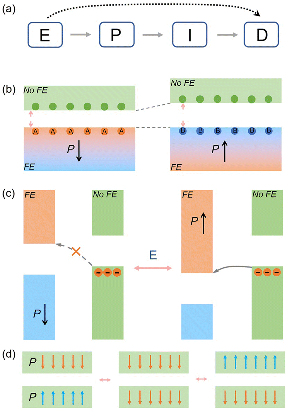 | ||
| Fig. 1 (a) The EPID mechanism. (b)–(d) Three mechanisms for realizing the electric field switching of the distances of the 2D lattice in a reversible and nonvolatile fashion. “FE” and “No FE” represent the ferroelectric layer and ordinary layer, respectively. | ||
(2) In the EPID-II case, as shown in Fig. 1c, the bilayer also contains one FE layer and one ordinary layer. However, unlike the EPID-I case, the two terminated surfaces of the FE layer are identical. Assuming that there are two different band offsets when the two surfaces of the FE layer are in contact with the ordinary layer (i.e., one is a type-II band alignment, and the other is a type-III band alignment), a significant difference in the charge transfer between the two layers can be expected under FE switching. This would change the interlayer interaction and the overall material thickness, giving rise to the nonvolatile electric field switching of its distance.
(3) In the EPID-III case, as shown in Fig. 1d, the structure contains two FE layers. In this case, unlike the EPID-I and EPID-II, there is no difference in the interface and band alignment for the two different polarization configurations. However, due to the different dipole–dipole interactions manipulated by FE switching, different interlayer interactions can occur, thus leading to the nonvolatile electric field switching of its distance.
EPID-I: differences in terminated surfaces
After establishing the three types of EPID mechanisms, we will next discuss their realization in real materials. For the EPID-I case, we selected the single-layered (SL) ReIrGe2S6 as the constituent FE layer. Fig. S1 (ESI†) shows the crystal structure of SL ReIrGe2S6. The terminated surfaces are formed by S and Ge atoms, respectively. Although there will be some Re and Ir atoms in the terminal surface in experiments, Ge and S atoms that cause interface differences are dominant. Such a structure gives rise to an out-of-plane electric polarization of 4.16 × 10⁻³ C m−2. Because the two Ge atomic layers can be displaced up and down, the electric polarization can be reversed, giving rise to the FE behavior of SL ReIrGe2S6. Intriguingly, along with the FE switching, the terminated surface of SL ReIrGe2S6 would also be reversed, which provides the possibility for realizing the EPID-I mechanism upon contact with another ordinary layer. Here, we selected SL MoS2 as the ordinary layer and used a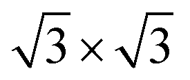 supercell MoS2 to match a 1 × 1 unit cell ReIrGe2S6. The lattice mismatch between them is only about 3%, indicating the high experimental feasibility.
Given the structure of ReIrGe2S6, we constructed two types of MoS2/ReIrGe2S6 bilayers: one with electric polarization pointing away from the interface (P↓), and the other with electric polarization pointing to the interface (P↑). The most stable crystal structures of P↓ and P↑ are displayed in Fig. 2a and b, which can be considered as two FE states of the MoS2/ReIrGe2S6 bilayer. In the P↓ configuration, the terminated surfaces from MoS2 and ReIrGe2S6 at the interface are both formed by S atoms. Due to the repulsion of these two S atomic layers, there is a large interlayer distance (d) of 3.208 Å and a large atomic thickness (AT) of 9.738 Å. Unlike the P↓ configuration, in the P↑ configuration, the terminated surfaces from MoS2 and ReIrGe2S6 at the interface are formed by S and Ge atoms, respectively. Considering their different electronegativities, the repulsion between S and Ge atomic layers would be much smaller than that between S and S atomic layers, yielding significantly smaller d = 2.581 Å and AT = 9.104 Å for the P↑ configuration. The differences in d and AT for these two configurations are 0.627 Å and 0.634 Å respectively. Assuming that these two configurations can be reversed under FE switching, the nonvolatile electric field switching of dimensions was realized in MoS2/ReIrGe2S6. We wish to point out that the ratio of electro-mechanical coupling is about 19.5%/24.3% (the ratio of electro-mechanical coupling is defined as (dstate-I/dstate-II−1) × 100%, where dstate-I and dstate-II are the interlayer distances for state-I and state-II, respectively), which is compared with conventional three-dimensional materials of ceramic lead lanthanum zirconate titanate.40 Such a large electro-mechanical coupling ratio is rarely reported in 2D systems.41
 | ||
| Fig. 2 Crystal structures of the MoS2/ReIrGe2S6 bilayer in the P↓ (a) and P↑ (b) configurations. Green, blue, gray, orange, and red spheres represent S, Ge, Re, Ir, and Mo atoms, respectively. (c) Minimum energy pathway of FE switching as a function of step number within the Climbing Image Nudged Elastic Band (CI-NEB) for the MoS2/ReIrGe2S6 bilayer. (d) Variation of d and AT as a function of step number within CI-NEB for the MoS2/ReIrGe2S6 bilayer. | ||
To estimate the feasibility of ferroelectricity in the MoS2/ReIrGe2S6 bilayer, we investigated its FE transformation process. Fig. 2c presents the minimum energy pathway of FE switching as a function of step number within CI-NEB for the MoS2/ReIrGe2S6 bilayer. The FE switching barrier from P↑ (P↓) to P↓ (P↑) was calculated to be 0.74 (0.59) eV per unit cell. These values are comparable with those of GaTeCl (0.754 eV per unit cell), vacancy-doped CrI3 (0.65 eV per unit cell) and SbN (0.604 eV per unit cell).42–44 This indicates the feasibility of the ferroelectricity, as well as the nonvolatile electric field switching of dimensions, in MoS2/ReIrGe2S6. Fig. 2d summarizes the variation of d and AT as a function of step number within CI-NEB. AT shows a trend of decreasing first and then increasing, indicating a nonlinear relation with the step number. The band structures of the P↑ and P↓ configurations are shown in Fig. S5 (ESI†). Both are semiconductors, indicating that ferroelectric switching does not essentially change the semiconducting properties of MoS2/ReIrGe2S6. This is different from the case of EPID-II, as we will discuss in the following. This mechanism can be extended to all ferroelectric materials, wherein the polarization switching can alter the type of interfacial atoms, such as NbN, SiN, and so on.
EPID-II: differences in band offsets
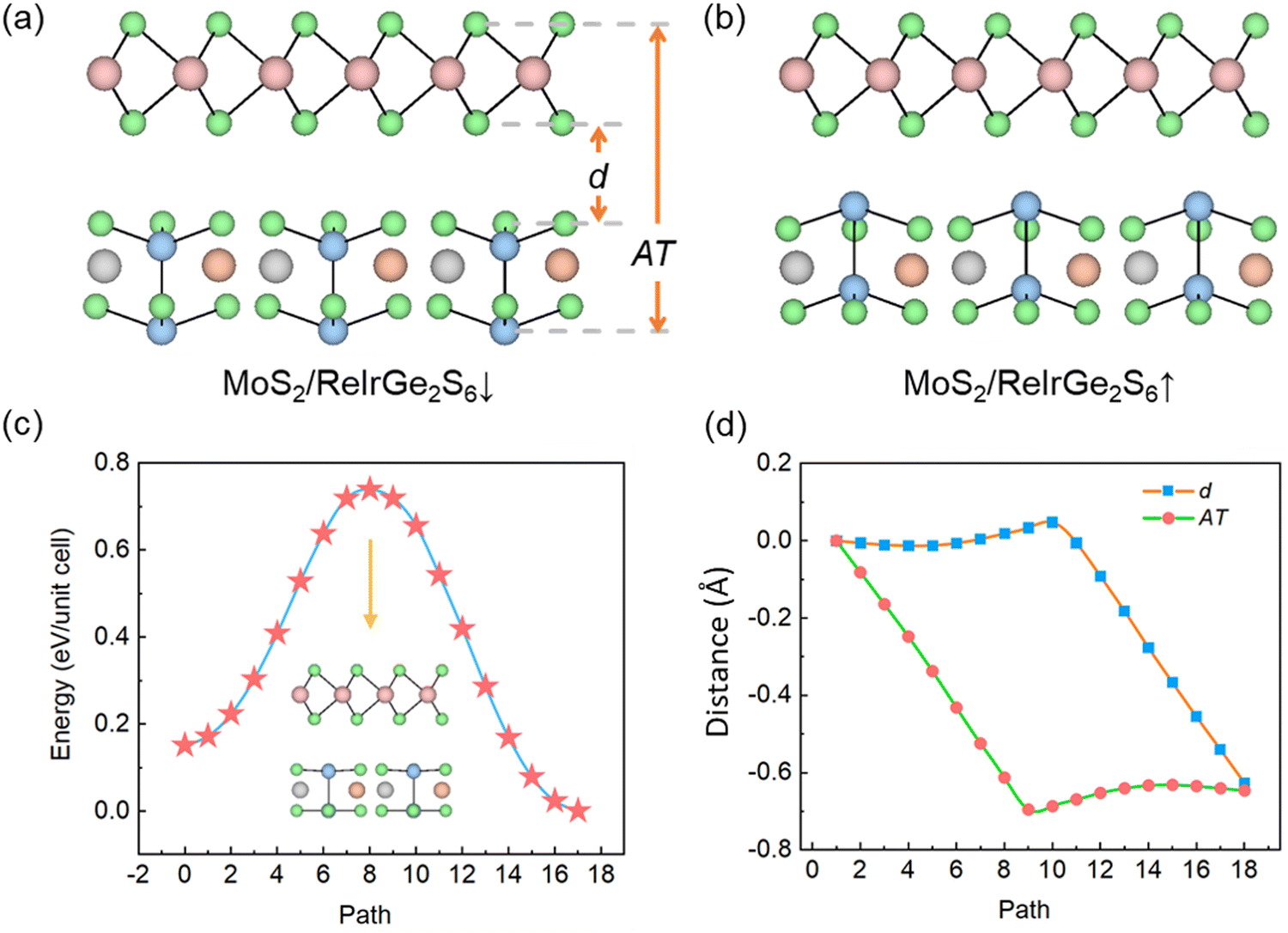
For the EPID-II case, we selected SL In2Se3 as the constituent FE layer. As shown in Fig. 3(a) and (b), different from SL ReIrGe2S6, the two terminated surfaces of SL In2Se3 are both formed by Se atoms. However, the asymmetric positions of Se atoms in the middle layer result in different coordination environments of In atoms and thus break the centrosymmetry, leading to an out-of-plane electric polarization of 2.31 × 10⁻³ C m−2. Due to the existence of the large electric polarization, the work functions of the two surfaces of SL In2Se3 are significantly different, which were calculated to be 4.2 and 6.5 eV, respectively. Such a large difference in work function is beneficial for realizing the two different types of band alignments on the two surfaces. In this regard, the ordinary layer should harbor a work function close to one surface of SL In2Se3. Here, we selected SL Sb, exhibiting a work function of 4.6 eV, as the ordinary layer. The Sb monolayer was realized in recent experiments.45 Because of the sp3 hybridization, it shows the buckled honeycomb lattice. The Sb/In2Se3 bilayer was constructed by using use a unit cell Sb to match a unit cell In2Se3. The lattice mismatch between them is within 2%, which suggests its experimental feasibility.46 | ||
| Fig. 3 (a) and (b) Crystal structures of the Sb/In2Se3 bilayer under P↑ and P↓ configurations. Orange, blue, and red spheres represent Sb, In, and Se atoms, respectively. (c) and (d) Band structures of the Sb/In2Se3 bilayer under P↑ and P↓ configurations. (e) The variation of d and AT as a function of step number within the CI-NEB for the Sb/In2Se3 bilayer. | ||
Similar to MoS2/ReIrGe2S6, we also constructed two types of Sb/In2Se3 bilayer: one with electric polarization pointing away from the interface (P↓), and the other with electric polarization pointing to the interface (P↑). Fig. 3a and b display the most stable crystal structures of P↑ and P↓ configurations, which are the two FE states of the Sb/In2S3 bilayer. The corresponding band structures of these two configurations are shown in Fig. 3c and d. For the P↑ configuration, the CBM from the In2Se3 layer is located above the Fermi level, while the VBM from the Sb layer lies below the Fermi level, giving rise to a direct band gap of 1.41 eV at the Γ point. A type-II band alignment forms between the band edges of SL In2Se3 and Sb in the P↑ configuration. For the P↓ configuration, as illustrated in Fig. 3d, the CBM from the In2Se3 layer shifts below the Fermi level, while the VBM from the Sb layer shifts above the Fermi level, indicating a type-III band alignment for the band edges of In2Se3 and Sb layers.
Due to the different band alignments in the P↑ and P↓ configurations of the Sb/In2Se3 bilayer, the charge transfers at the interfaces would also be different for the two configurations. Fig. S6 (ESI†) shows the charge density differences between the two layers for the Sb/In2Se3 bilayer. For the P↑ configuration, the charge densities are mainly localized in the space between the two layers, in good agreement with the type-II band alignment. For the P↓ configuration, significant electron transfer occurs between Sb and In2S3 layers, as shown in Fig. S3 (ESI†). Therefore, with respect to the P↑ configuration, a stronger interlayer interaction is achieved in the P↓ configuration. According to the EPID mechanism, this would result in different d and AT for these two configurations. Our calculations show that the d and AT are 2.935 (2.789) Å and 11.485 (11.315) Å, respectively, for P↑ (P↓) configurations. The differences in d and AT for these two configurations are 0.146 Å and 0.17 Å respectively. The ratio of electro-mechanical coupling is about 5.2%/5.0%. To estimate the feasibility of ferroelectricity in Sb/In2Se3, we investigate its FE transformation process. As shown Fig. S7 and S8 (ESI†), the transitions between P↓ and P↑ occur through the concerted motion of the lower three Se–In–Se layers, as illustrated in Fig. S7 (ESI†). In detail, the transition between P↓ and the paraelectric state is realized by the left shifting of the lower In–Se layer and the upper-inclined shifting of the inner Se layer, and the transition between the paraelectric state and P↑ phases is caused by the right shifting of the lower In–Se layer and the upper-inclined shifting of the inner Se layer. The lattice parameters hardly change during the transformation process. The FE switching barrier from P↑ (P↓) to P↓ (P↑) is calculated to be 0.295 (0.355) eV per unit cell, which is comparable with that of CrB2 (0.363 eV per unit cell), and smaller than that of Sc2CO2 (0.52 eV per unit cell), vacancy-doped CrI3 (0.65 eV per unit cell) and GaTeCl (0.754 eV per unit cell).42,43,47,48 This indicates the feasibility of the ferroelectricity, as well as the nonvolatile electric field switching of dimensions, in Sb/In2Se3. The variations of d and AT as a function of step number within CI-NEB for the Sb/In2Se3 bilayer are displayed in Fig. 3e. Different from the case of MoS2/ReIrGe2S6, AT showed a roughly linear relation with the step number. We select another candidate, monolayer PdTe2, to further verify this mechanism. As shown in Fig. S9 (ESI†), the two polarization configurations of PdTe2/In2Se3 exhibit different band alignments according to our mechanism. By reversing the ferroelectric polarization direction of In2Se3, we could still achieve the switching of the interlayer distance. We can extend this mechanism to similar systems, such as Bi/In2Se3, MnSe/In2S3, PtTe2/In2Se3, and so on.
EPID-III: differences in dipole–dipole interactions
We have used the bilayer In2Se3 as an example to discuss the realization of the EPID-III mechanism. Considering the alignment of electric polarizations in the constituent layers, we constructed three types of bilayer In2Se3: one with two electric polarizations pointing along the +z direction (P↑↑), one with electric polarization pointing away from the interface (P↑↓) and another with electric polarization pointing to the interface (P↓↑), as shown in Fig. 4. As expected, due to the different dipole–dipole interactions, the AT are different for these three configurations. The AT were calculated to be 17.426 Å, 17.389 Å and 17.475 Å, respectively, for P↑↑, P↑↓ and P↓↑ configurations. The ratio of electro-mechanical coupling is about 1.3% or 3.2%. As these three configurations can be reversed under FE switching, quite naturally, the nonvolatile electric field switching of dimensions is realized in bilayer In2Se3. The ferroelectric transition between P↓ and P↑ in In2Se3 is the same as EPID-II, as shown in Fig. S10 (ESI†). The lattice parameters also hardly change during the transformation process. The results produced by this mechanism are general in two-dimensional ferroelectric materials exhibiting z-direction polarization, such as AgBiP2S6, CuCrP2Se6, and so on.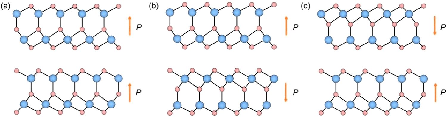 | ||
| Fig. 4 Crystal structures of bilayer In2Se3 under different polarization configurations. (a) Two electric polarizations point along the +z direction (P↑↑). (b) Two electric polarizations point away from the interface (P↑↓). (c) Two electric polarizations point to the interface (P↓↑). Blue and red spheres represent In and Se atoms, respectively. | ||
Discussion
For the experimental realizations of these heterobilayer systems, the most used fabrication is by a stepwise mechanical transfer of specific 2D layers onto a substrate, i.e., by the top-down manipulation of individual nanosheets one by one.49 It should be noted that in the In2Se3 system, the ferroelectric inversion was experimentally realized under the external electric field (7 V/30 nm). For the corresponding heterobilayers, the switching of the ferroelectricity might be achieved under a comparable external electric field.Conclusions
We have identified a novel mechanism for realizing the electric field switching of the dimensions of a 2D lattice in a reversible and nonvolatile fashion. This mechanism is through the mediation of the strength of interlayer interactions in 2D FE bilayer systems. Using first-principles calculations, we validated this mechanism in a series of real 2D bilayer materials, e.g., MoS2/ReIrGe2S6, Sb/In2Se3, and bilayer In2Se3. The underlying physics is discussed in detail. Our work provides a new direction and method for electro-mechanical coupling in the 2D lattice.Methods
The first-principles calculations
All calculations based on density functional theory (DFT) were performed using the Vienna ab initio Simulation Package (VASP).50 The exchange–correlation interaction was treated by the generalized gradient approximation (GGA) parametrized by Perdew, Burke, and Ernzerhof (PBE). The ion-electron interaction was treated by the projector-augmented wave method (PAW).51,52 The Monkhorst–Pack k-mesh was set to 9 × 9 × 1. The kinetic cutoff energy was set to 550 eV. All structures were fully relaxed until the force on each atom was less than 0.01 eV Å−1. The electronic iteration convergence criterion was set to 1 × 10⁻⁵ eV. To avoid spurious interactions between periodic images, a vacuum space of at least 15 Å was introduced. The DFT-D3 method was employed for treating van der Waals (vdW) interactions in all calculations.53 The DFT-D2 and PBEsol methods were also used to calculate the band structures, which gave roughly similar band offsets. The ferroelectric transition pathway and energy barrier were calculated based on the CI-NEB method.54 Dipole moment correction was employed in all the calculations.55Author contributions
X.X. conceived the idea of the project and run all simulations with inputs from Y.M and Y.D. X.X., T.Z., Y.M., B.H., and Y.D. analyzed the data. All authors discussed the results and contributed to the writing of the manuscript.Conflicts of interest
The authors declare no conflict of interest.Acknowledgements
This work is supported by the National Natural Science Foundation of China (No. 12274261 and 12074217), Shandong Provincial Science Foundation for Excellent Young Scholars (No. ZR2020YQ04), Shandong Provincial Key Research and Development Program (Major Scientific and Technological Innovation Project) (No. 2019JZZY010302), Shandong Provincial QingChuang Technology Support Plan (No. 2021KJ002), and Taishan Young Scholar Program of Shandong Province.References
- Y. E. Pak, Circular Inclusion Problem in Antiplane Piezoelectricity, Int. J. Fract., 1992, 54, 79 CrossRef CAS.
- K. Uchino, Piezoelectric Actuators and Ultrasonic Motors, Kluwer Academic, Boston, 1996 Search PubMed.
- M. Kamlah and C. Tsakmakis, Phenomenological Modeling of the Non-Linear Electro-Mechanical Coupling in Ferroelectrics, Int. J. Solids Struct., 1999, 36, 669 CrossRef.
- Z. L. Wang and J. Song, Piezoelectric Nanogenerators Based on Zinc Oxide Nanowire Arrays, Science, 2006, 312, 242 CrossRef CAS PubMed.
- X. Wang, J. Song, J. Liu and Z. L. Wang, Direct-Current Nanogenerator Driven by Ultrasonic Waves, Science, 2007, 316, 102 CrossRef CAS PubMed.
- A. Pramanick, D. Damjanovic, J. E. Daniels, J. C. Nino and J. L. Jones, Origins of Electro-Mechanical Coupling in Polycrystalline Ferroelectrics during Subcoercive Electrical Loading, J. Am. Ceram. Soc., 2011, 94, 293 CrossRef CAS.
- J. F. Nye, Physical Properties of Crystals, Oxford U. P., Oxford, England, 1957, Chap. 10 Search PubMed.
- R. M. Martin, Piezoelectricity, Phys. Rev. B, 1972, 5, 1607 CrossRef.
- A. K. Tagantsev, Piezoelectricity and Flexoelectricity in Crystalline Dielectrics, Phys. Rev. B, 1986, 34, 5883 CrossRef PubMed.
- H. F. Kay, Electrostriction, Rep. Prog. Phys., 1955, 18, 230 CrossRef.
- J. Grindlay, Electrostriction, Phys. Rev., 1967, 160, 698 CrossRef CAS.
- P. Prior and B. J. Roth, Electrostriction of Anisotropic Tissue, Phys. Rev. E, 2007, 75, 021903 CrossRef PubMed.
- V. Sundar and R. E. Newnham, Electrostriction and Polarization, Ferroelectrics, 1992, 135, 431 CrossRef CAS.
- Z. Liu, L. Wang, X. Yu, J. Zhang, R. Yang, X. Zhang, Y. Ji, M. Wu, L. Deng, L. Li and Z. Wang, Piezoelectric-Effect-Enhanced Full-Spectrum Photoelectrocatalysis in p–n Heterojunction, Adv. Funct. Mater., 2019, 29, 1807279 CrossRef CAS.
- S. Zhang, Z. Liu, M. Ruan, Z. Guo, E. Lei, W. Zhao, D. Zhao, X. Wu and D. Chen, Enhanced Piezoelectric-Effect-Assisted Photoelectrochemical Performance in ZnO Modified with Dual Cocatalysts, Appl. Catal., B, 2020, 262, 118279 CrossRef CAS.
- Y. Jiang, M. Li, Y. Mi, L. Guo, W. Fang, X. Zeng, T. Zhou and Y. Liu, The Influence of Piezoelectric Effect on The Heterogeneous Photocatalytic Hydrogen Production of Strontium Titanate Nanoparticles, Nano Energy, 2021, 85, 105949 CrossRef CAS.
- M. Fattouhi, F. García-Sánchez, R. Yanes, V. Raposo, E. Martínez and L. Lopez-Diaz, Electric Field Control of the Skyrmion Hall Effect in Piezoelectric-Magnetic Devices, Phys. Rev. Appl, 2021, 16, 044035 CrossRef CAS.
- M. Chazono, H. Watanabe and Y. Yanase, Superconducting Piezoelectric Effect, Phys. Rev. B, 2022, 105, 024509 CrossRef CAS.
- R. Peng and J. Liu, Topological Piezoelectric Response in Moiré Graphene Systems, Phys. Rev. Res., 2022, 4, L032006 CrossRef CAS.
- J. Yu and P.-E. Janolin, Defining “Giant” Electrostriction, J. Appl. Phys., 2022, 131, 170701 CrossRef CAS.
- M.-B. Rubén, G.-N. Cristina, G.-H. Julio and Z. Félix, 2D Materials: to Graphene and Beyond, Nanoscale, 2011, 3, 20 RSC.
- A. Gupta, T. Sakthivel and S. Seal, Recent Development in 2D Materials beyond Graphene, Prog. Mater. Sci., 2015, 73, 44 CrossRef CAS.
- R. Hinchet, U. Khan, C. Falconi and S.-W. Kim, Piezoelectric Properties in Two-Dimensional Materials: Simulations and Experiments, Mater. Today, 2018, 21, 611 CrossRef CAS.
- M. Dai, Z. Wang, F. Wang, Y. Qiu, J. Zhang, C.-Y. Xu, T. Zhai, W. Cao, Y. Fu, D. Jia, Y. Zhou and P.-A. Hu, Two-Dimensional van der Waals Materials with Aligned In-Plane Polarization and Large Piezoelectric Effect for Self-Powered Piezoelectric Sensors, Nano Lett., 2019, 19, 5410 CrossRef CAS PubMed.
- M. Dai, W. Zheng, X. Zhang, S. Wang, J. Lin, K. Li, Y. Hu, E. Sun, J. Zhang, Y. Qiu, Y. Fu, W. Cao and P.-A. Hu, Enhanced Piezoelectric Effect Derived from Grain Boundary in MoS2 Monolayers, Nano Lett., 2020, 20, 201 CrossRef CAS PubMed.
- P. C. Sherrell, M. Fronzi, N. A. Shepelin, A. Corletto, D. A. Winkler, M. Ford, J. G. Shapter and A. V. Ellis, A Bright Future for Engineering Piezoelectric 2D Crystals, Chem. Soc. Rev., 2022, 51, 650 RSC.
- W. Ding, J. Zhu, Z. Wang, Y. Gao, D. Xiao, Y. Gu, Z. Zhang and W. Zhu, Prediction of Intrinsic Two-Dimensional Ferroelectrics in In2Se3 and Other III2-VI3 van der Waals Materials, Nat. Commun., 2017, 8, 14956 CrossRef CAS PubMed.
- L. Li and M. Wu, Binary Compound Bilayer and Multilayer with Vertical Polarizations: Two-Dimensional Ferroelectrics, Multiferroics, and Nanogenerators, ACS Nano, 2017, 11, 6382 CrossRef CAS PubMed.
- B. Xu, H. Xiang, Y. Xia, K. Jiang, X. Wan, J. He, J. Yin and Z. Liu, Monolayer AgBiP2Se6: An Atomically Thin Ferroelectric Semiconductor with Out-Plane Polarization, Nanoscale, 2017, 9, 8427 RSC.
- M. Wu and X. C. Zeng, Intrinsic Ferroelasticity and/or Multiferroicity in Two-Dimensional Phosphorene and Phosphorene Analogues, Nano Lett., 2016, 16, 3236 CrossRef CAS PubMed.
- Z. Guan, H. Hu, X. Shen, P. Xiang, N. Zhong, J. Chu and C. Duan, Recent Progress in Two-Dimensional Ferroelectric Materials, Adv. Electron. Mater., 2020, 6, 1900818 CrossRef CAS.
- B. Behera, B. C. Sutar and N. R. Pradhan, Recent Progress on 2D Ferroelectric and Multiferroic Materials, Challenges, and Opportunity, Emergent Mater., 2021, 4, 847 CrossRef CAS.
- A. Belianinov, Q. He, A. Dziaugys, P. Maksymovych, E. Eliseev, A. Borisevich, A. Morozovska, J. Banys, Y. Vysochanskii and S. V. Kalinin, CuInP2S6 Room Temperature Layered Ferroelectric, Nano Lett., 2015, 15, 3808 CrossRef CAS PubMed.
- F. Liu, L. You, K. L. Seyler, X. Li, P. Yu, J. Lin, X. Wang, J. Zhou, H. Wang, H. He, S. T. Pantelides, W. Zhou, P. Sharma, X. Xu, P. M. Ajayan, J. Wang and Z. Liu, Room-Temperature Ferroelectricity in CuInP2S6 Ultrathin Flakes, Nat. Commun., 2016, 7, 12357 CrossRef CAS PubMed.
- K. Chang, J. Liu, H. Lin, N. Wang, K. Zhao, A. Zhang, F. Jin, Y. Zhong, X. Hu, W. Duan, Q. Zhang, L. Fu, Q.-K. Xue, X. Chen and S.-H. Ji, Discovery of Robust In-Plane Ferroelectricity in Atomic-Thick SnTe, Science, 2016, 353, 274 CrossRef CAS PubMed.
- Y. Zhou, D. Wu, Y. Zhu, Y. Cho, Q. He, X. Yang, K. Herrera, Z. Chu, Y. Han, M. C. Downer, H. Peng and K. Lai, Out-of-Plane Piezoelectricity and Ferroelectricity in Layered α-In2Se3 Nanoflakes, Nano Lett., 2017, 17, 5508 CrossRef CAS PubMed.
- C. Cui, W.-J. Hu, X. Yan, C. Addiego, W. Gao, Y. Wang, Z. Wang, L. Li, Y. Cheng, P. Li, X. Zhang, H. N. Alshareef, T. Wu, W. Zhu, X. Pan and L.-J. Li, Intercorrelated In-Plane and Out-of-Plane Ferroelectricity in Ultrathin Two-Dimensional Layered Semiconductor In2Se3, Nano Lett., 2018, 18, 1253 CrossRef CAS PubMed.
- D.-Y. Guo, C.-W. Chen, C.-C. Li, H.-C. Jau, K.-H. Lin, T.-M. Feng, C.-T. Wang, T. J. Bunning, I. Choon Khoo and T.-H. Lin, Reconfiguration of Three-Dimensional Liquid-Crystalline Photonic Crystals by Electrostriction, Nat. Mater., 2020, 19, 94 CrossRef CAS PubMed.
- N. Yavo, A. D. Smith, O. Yeheskel, S. Cohen, R. Korobko, E. Wachtel, P. R. Slater and I. Lubomirsky, Large Nonclassical Electrostriction in (Y, Nb)-Stabilized δ-Bi2O3, Adv. Funct. Mater., 2016, 26, 1138 CrossRef CAS.
- S. C. Hwang, C. S. Lynch and R. M. Mcmeeking, Ferroelectric/Ferroelastic Interactions and A Polarization Switching Model, Acta Metal. Mater., 1995, 43, 2073 CrossRef CAS.
- Y. Gao, M. Gao and Y. Lu, Two-Dimensional Multiferroics, Nanoscale, 2021, 13, 19324 RSC.
- S.-H. Zhang and B.-G. Liu, A Controllable Robust Multiferroic GaTeCl Monolayer with Colossal 2D Ferroelectricity and Desirable Multifunctionality, Nanoscale, 2018, 10, 5990 RSC.
- C. Liu, W. Wan, J. Ma, W. Guo and Y. Yao, Robust Ferroelectricity in Two-Dimensional SbN and BiP, Nanoscale, 2018, 10, 7984 RSC.
- Y. Zhao, L. Lin, Q. Zhou, Y. Li, S. Yuan, Q. Chen, S. Dong and J. Wang, Surface Vacancy-Induced Switchable Electric Polarization and Enhanced Ferromagnetism in Monolayer Metal Trihalides, Nano Lett., 2018, 18, 2943 CrossRef CAS PubMed.
- P. Ares, F. Aguilar-Galindo, D. Rodríguez-San-Miguel, D. A. Aldave, S. Díaz-Tendero, M. Alcamí, F. Martín, J. Gómez-Herrero and F. Zamora, Mechanical isolation of highly stable antimonene under ambient conditions, Adv. Mater., 2016, 28, 6332 CrossRef CAS PubMed.
- J.-J. Zhang, D. Zhu and B. I. Yakobson, Heterobilayer with Ferroelectric Switching of Topological State, Nano Lett., 2021, 21, 785 CrossRef CAS PubMed.
- W. Luo, K. Xu and H. Xiang, Two-Dimensional Hyperferroelectric Metals: A Different Route to Ferromagnetic-Ferroelectric Multiferroics, Phys. Rev. B, 2017, 96, 235415 CrossRef.
- A. Chandrasekaran, A. Mishra and A. K. Singh, Ferroelectricity, Antiferroelectricity, and Ultrathin 2D Electron/Hole Gas in Multifunctional Monolayer MXene, Nano Lett., 2017, 17, 3290 CrossRef CAS PubMed.
- B. V. Lotsch, Vertical 2D Heterostructures, Annu. Rev. Mater. Res., 2015, 45, 85 CrossRef CAS.
- G. Kresse and J. Furthmuller, Efficient Iterative Schemes for ab initio Total-Energy Calculations using a Plane-Wave Basis Set, Phys. Rev. B, 1996, 54, 11169 CrossRef CAS PubMed.
- J. P. Perdew, K. Burke and M. Ernzerhof, Generalized Gradient Approximation Made Simple, Phys. Rev. Lett., 1996, 77, 3865 CrossRef CAS PubMed.
- G. Kresse and D. Joubert, From Ultrasoft Pseudopotentials to The Projector Augmented-Wave Method, Phys. Rev. B, 1999, 59, 1758 CrossRef CAS.
- S. Grimme, S. Ehrlich and L. Goerigk, Effect of The Damping Function in Dispersion Corrected Density Functional Theory, J. Comput. Chem., 2011, 32, 1456 CrossRef CAS PubMed.
- S. Guan, C. Liu, Y. Lu, Y. Yao and S. Yang, Tunable Ferroelectricity and Anisotropic Electric Transport in Monolayer β-GeSe, Phys. Rev. B, 2018, 97, 144104 CrossRef.
- J. Neugebauer and M. Scheffler, Adsorbate-Substrate and Adsorbate-Adsorbate Interactions of Na and K Adlayers on Al (111), Phys. Rev. B, 1992, 46, 16067 CrossRef CAS PubMed.
Footnote |
| † Electronic supplementary information (ESI) available. See DOI: https://doi.org/10.1039/d2nh00509c |
| This journal is © The Royal Society of Chemistry 2023 |