
2D Ruddlesden–Popper perovskite sensitized SnP2S6 ultraviolet photodetector enabling high responsivity and fast speed†
Yue
Zhang
a,
Fakun
Wang
b,
Xuan
Zhao
a,
Xin
Feng
a,
Na
Zhang
a,
Fangfang
Xia
a,
Ying
Ma
 a,
Huiqiao
Li
a and
Tianyou
Zhai
*a
a,
Huiqiao
Li
a and
Tianyou
Zhai
*a
aState Key Laboratory of Materials Processing and Die & Mould Technology, School of Materials Science and Engineering, Huazhong University of Science and Technology, Wuhan 430074, P. R. China. E-mail: zhaity@hust.edu.cn
bSchool of Electrical and Electronic Engineering, Nanyang Technological University, Singapore 639798, Singapore
First published on 18th November 2022
Abstract
As the newly developed wide-bandgap semiconductors, two-dimensional layered metal phosphorus chalcogenides (2D LMPCs) exhibit enormous potential applications in ultraviolet (UV) photodetection due to their superior optoelectronic performance. However, 2D LMPC-based UV photodetectors generally suffer from low responsivity and slow response speed, which hinder their practical applications. Here, we present an effective strategy of sensitizing 2D LMPC UV photodetectors with a 2D Ruddlesden–Popper (RP) perovskite to enable high responsivity and fast response speed. As a demonstration, a hybrid heterojunction composed of RP perovskite (PEA)2PbI4 and a 2D SnP2S6 flake is fabricated by spin-coating method. Benefitting from the strong optical absorption of (PEA)2PbI4 and the efficient interfacial charge transfer caused by the favorable type-II energy band alignment, the as-fabricated 2D SnP2S6/(PEA)2PbI4 hybrid heterojunction photodetectors show high responsivity (67.1 A W−1), large detectivity (2.8 × 10¹¹ Jones), fast rise/delay time (30/120 μs) and excellent external quantum efficiency (22825%) at 365 nm. Under field-effect modulation, the responsivity of the heterojunction photodetector can reach up to 239.4 A W−1, which is attributed to the photogating mechanism and reduced Schottky barriers. Owing to the excellent photodetection performance, the heterojunction device further shows superior imaging capability. This work provides an effective strategy for designing high-performance UV photodetectors toward future applications.
New conceptsTwo-dimensional layered metal phosphorus chalcogenides (2D LMPCs) are highly desired wide-bandgap semiconductors for ultraviolet (UV) photodetection. However, the 2D LMPC-based UV photodetectors commonly suffer from low responsivity and slow response speed, which seriously hinders their practical applications. In this work, taking advantage of the enhanced optical absorption as well as the favorable energy band alignment, a high-performance UV photodetector based on the 2D Ruddlesden–Popper (RP) perovskite (PEA)2PbI4 and SnP2S6 flake hybrid heterojunction has been demonstrated. In comparison to most 2D LMPC-based photodetectors, the heterojunction photodetector exhibits a high responsivity of 239.4 A W−1 and a fast response time of 30 μs at 365 nm, with great potential in photoelectric imaging applications. This work provides an efficient strategy for the design and fabrication of high-performance UV photodetectors toward multiple applications. |
1. Introduction
Ultraviolet (UV) photodetectors have drawn extensive attention for their wide application in military surveillance, optical communications, flame detection, environmental monitoring, and biological analysis.1–4 Two-dimensional layered metal phosphorus chalcogenides (2D LMPCs) with wide bandgaps of 1.3–4.5 eV are prospective candidates for next-generation UV photodetectors due to their excellent optoelectronic properties and ease of integration.5–7 Currently, tremendous efforts have been devoted to investigate the UV photodetection performance of 2D LMPCs with various compositions and structures.7–9 Despite the significant progress made in 2D LMPC-based UV photodetectors, most of them exhibit low responsivity and slow response speed, due to the weak optical absorption and inherent defect trapping caused by their atomically thin nature.8,10Constructing hybrid heterojunctions by combining 2D materials and photosensitizers with strong optical absorption has been demonstrated as an effective strategy to overcome the drawbacks mentioned above and achieve high-performance photodetectors.11–13 On the one hand, the hybrid heterojunctions combine the advantageous properties of two different materials, providing opportunities to break through the performance limitations of the single material.13,14 On the other hand, the built-in electric field formed at the hetero-interface facilitates the separation and transfer of photocarriers.15 The emerging 2D Ruddlesden–Popper (RP) perovskites are considered as suitable UV photosensitizers due to their wide bandgaps, large absorption coefficients, solution-processability and good environmental stability.16–18 For example, the 2D (BA)2MA3Pb4I13/MoS2 hybrid heterojunction fabricated by Xie et al. exhibits a high responsivity of 238 A W−1 and a fast response time at the microsecond level.19 Shen et al. demonstrated that the 2D (PEA)2PbI4 sensitized MoS2 photodetector shows a 100-fold improvement in the response speed (several milliseconds) relative to the pure MoS2 device.20 Therefore, hybridizing 2D RP perovskites together with 2D LMPCs is highly promising for realizing high-sensitivity and fast-speed UV photodetectors.
In this work, we present the first demonstration of a 2D RP perovskite-LMPC hybrid heterojunction for high-performance UV photodetectors. Herein, a typical RP perovskite (PEA)2PbI4 and an emerging LMPC SnP2S6 are selected as the photosensitizer layer and the carrier transport layer, respectively. Ultraviolet photoelectron spectroscopy (UPS) and photoluminescence (PL) spectra as well as fluorescence lifetime measurements reveal the type-II band alignment of the 2D SnP2S6/(PEA)2PbI4 hybrid heterojunction, which promotes efficient interfacial charge transfer from (PEA)2PbI4 to SnP2S6. Owing to the enhanced optical absorption and the efficient interfacial charge transfer, the 2D SnP2S6/(PEA)2PbI4 hybrid heterojunction photodetector has demonstrated 20-fold enhancement for responsivity (67.1 A W−1) and 50-fold improvement for response time (30 μs) than the pure SnP2S6 device at 365 nm. And the responsivity can be further increased to 239.4 A W−1 by the synergistic effect of the photogating mechanism and Schottky barrier reduction under field-effect modulation. In addition, the hybrid heterojunction shows excellent imaging capability, which is evidenced by a single-pixel imaging system. Our demonstration provides an effective strategy towards high-sensitivity and fast-speed UV photodetectors based on 2D RP perovskite–LMPC hybrid heterojunctions.
2. Results and discussion
Fig. 1a presents the specific fabrication process of the 2D SnP2S6/(PEA)2PbI4 hybrid heterojunction. First, the multilayer SnP2S6 flakes are mechanically exfoliated onto a 300 nm SiO2/Si substrate, as shown in Fig. 1b. The transmission electron microscopy (TEM) image of the SnP2S6 flake clearly shows two clear lattice spacing of 0.51 nm with an included angle of 60°, corresponding to (010) and (100) planes of rhombohedral SnP2S6 (Fig. 1c),21 which indicates that the as-exfoliated SnP2S6 flake possesses high crystallinity and cleaves along the (001) plane. Then the 2D perovskite (PEA)2PbI4 layer is deposited on the top of an as-exfoliated SnP2S6 sample using a facile solution spin-coating method at a spin speed of 3000 rpm for 60 s, followed by an annealing process on a hot plate at 80 °C for 10 min. It should be noted that the spin-coating process and the annealing process are carried out in a glove box. Finally, the 2D SnP2S6/(PEA)2PbI4 hybrid heterojunction is successfully obtained, as shown in Fig. 1d. The scanning electron microscopy (SEM) image and energy dispersive spectroscopy (EDS) mapping have confirmed that the prepared (PEA)2PbI4 layer possesses completely dense morphology and uniform elemental distribution of C, N, Pb and I (Fig. S1, ESI†). The atomic force microscopy (AFM) image of the heterojunction surface is shown in Fig. 1e. The polycrystalline (PEA)2PbI4 layer deposited on the SnP2S6 flake shows an average grain size of 20–50 nm and continuous surface coverage. To further characterize the structure of the 2D SnP2S6/(PEA)2PbI4 heterojunction, X-ray diffraction (XRD) measurement was conducted. As shown in Fig. 1f, the peaks at 13.7°, 27.6° and 56.8° can be assigned to the (003), (006) and (0012) crystallographic planes of 2D SnP2S6, and the peaks at 5.5°, 10.9°, 16.3°, 21.8°, 27.4° and 32.9° correspond to the (002), (004), (006), (008), (0010) and (0012) crystallographic planes of 2D perovskite (PEA)2PbI4.22,23 Besides, the characteristic peaks of SnP2S6 and (PEA)2PbI4 can be simultaneously detected in their heterojunction and no additional peaks have appeared, which indicates the successful combination of the (PEA)2PbI4 layer and the SnP2S6 flake. The optical characteristics of the heterojunction are investigated using ultraviolet-visible absorption spectra. As shown in Fig. 1g, the SnP2S6 flake exhibits obvious absorption at 300–500 nm, which results from the optical transition between the valence and the conduction band.24 For (PEA)2PbI4, strong absorption at 300–550 nm has been observed, while the sharp absorption peak at about 524 nm can be attributed to the excitonic transition.25 In comparison, the SnP2S6/(PEA)2PbI4 heterojunction retains the absorption characteristics of (PEA)2PbI4 and presents enhanced absorption at 300–500 nm, which is caused by the co-absorption of SnP2S6 and (PEA)2PbI4.26 | ||
| Fig. 1 Preparation and characterization of the SnP2S6/(PEA)2PbI4 heterojunction. (a) Schematic diagram of the SnP2S6/(PEA)2PbI4 heterojunction prepared by a spin-coating method. (b) Optical image of SnP2S6 flakes before spin-coating (PEA)2PbI4. (c) TEM image of the SnP2S6 flake. (d) Optical image of SnP2S6 flakes after spin-coating (PEA)2PbI4. (e) AFM image of the (PEA)2PbI4 layer deposited on the SnP2S6 flakes. (f) XRD patterns and (g) absorption spectra of the SnP2S6 flake, the (PEA)2PbI4 layer and the heterojunction. (h) Band alignment of the SnP2S6/(PEA)2PbI4 heterojunction. | ||
To better understand the energy band structure of the heterojunction, we have performed ultraviolet photoelectron spectroscopy (UPS) measurements. The UPS results of SnP2S6 and (PEA)2PbI4 are shown in Fig. S2 (ESI†). The work function (WF) of SnP2S6 and (PEA)2PbI4 can be calculated to be 5.22 eV and 4.47 eV according to WF = hν − Es, where hν and Es refer to the photon energy (21.22 eV for the He I light source) and the second electron cutoff energy, respectively. Therefore, the Fermi level (EF) of SnP2S6 and (PEA)2PbI4 is determined to be −5.22 eV and −4.47 eV when the vacuum level is taken as the reference. As can be seen from the valence band spectra, the difference between the valence band maximum (Ev) and the EF of SnP2S6 and (PEA)2PbI4 is 1.51 eV and 1.1 eV. The Ev of SnP2S6 and (PEA)2PbI4 can be estimated to be −6.62 eV and −5.26 eV, respectively. Subsequently, the optical band gap of SnP2S6 and (PEA)2PbI4 is determined to be 2.5 eV and 2.3 eV,21,22 and thus a type-II band alignment of the SnP2S6/(PEA)2PbI4 heterojunction is proposed in Fig. 1.
According to previous reports, SnP2S6 is an n-type semiconductor while (PEA)2PbI4 is commonly considered as a p-type semiconductor.27,28 When SnP2S6 and (PEA)2PbI4 are in contact with each other, a depletion region would form, and the EF gradually tends to align and reaches a new equilibrium as the electrons diffuse from (PEA)2PbI4 into SnP2S6.29,30 Benefitting from the charge transfer, the energy band at the interface would bend and a stable built-in electric field with barrier height of 0.7 eV (the EF difference of two materials) is established on both sides of the interface.31,32 Therefore, the photoexcited electron–hole pairs in (PEA)2PbI4 are separated by the built-in electric field, leading to electrons diffusing into SnP2S6 while the holes are retained in (PEA)2PbI4, as presented in Fig. 2a.20,33 To further explore the interfacial carrier dynamics, the steady-state photoluminescence (PL) and fluorescence lifetime measurements have been conducted. Generally, the photo-generated electron–hole pairs in the (PEA)2PbI4 layer would recombine rapidly. However, after being combined with the SnP2S6 flake, the transfer of electrons into SnP2S6 would effectively reduce the rate of photo-generated electrons and holes recombination in (PEA)2PbI4, resulting in the quenching of PL intensity and the shortening of the fluorescence lifetime, as shown in Fig. 2b and c.13,34 In order to gain a clearer understanding of charge transfer at the interface, the PL intensity mapping and fluorescence lifetime imaging are performed on the region shown in Fig. 2d. As shown in Fig. 2e and f, the outline of the dark SnP2S6 flake can be clearly resolved, indicating that the PL intensity and the fluorescence lifetime of (PEA)2PbI4 are significantly suppressed after being combined with SnP2S6. These results confirmed that such type-II band alignment of the SnP2S6/(PEA)2PbI4 heterojunction could facilitate efficient charge separation and transfer.
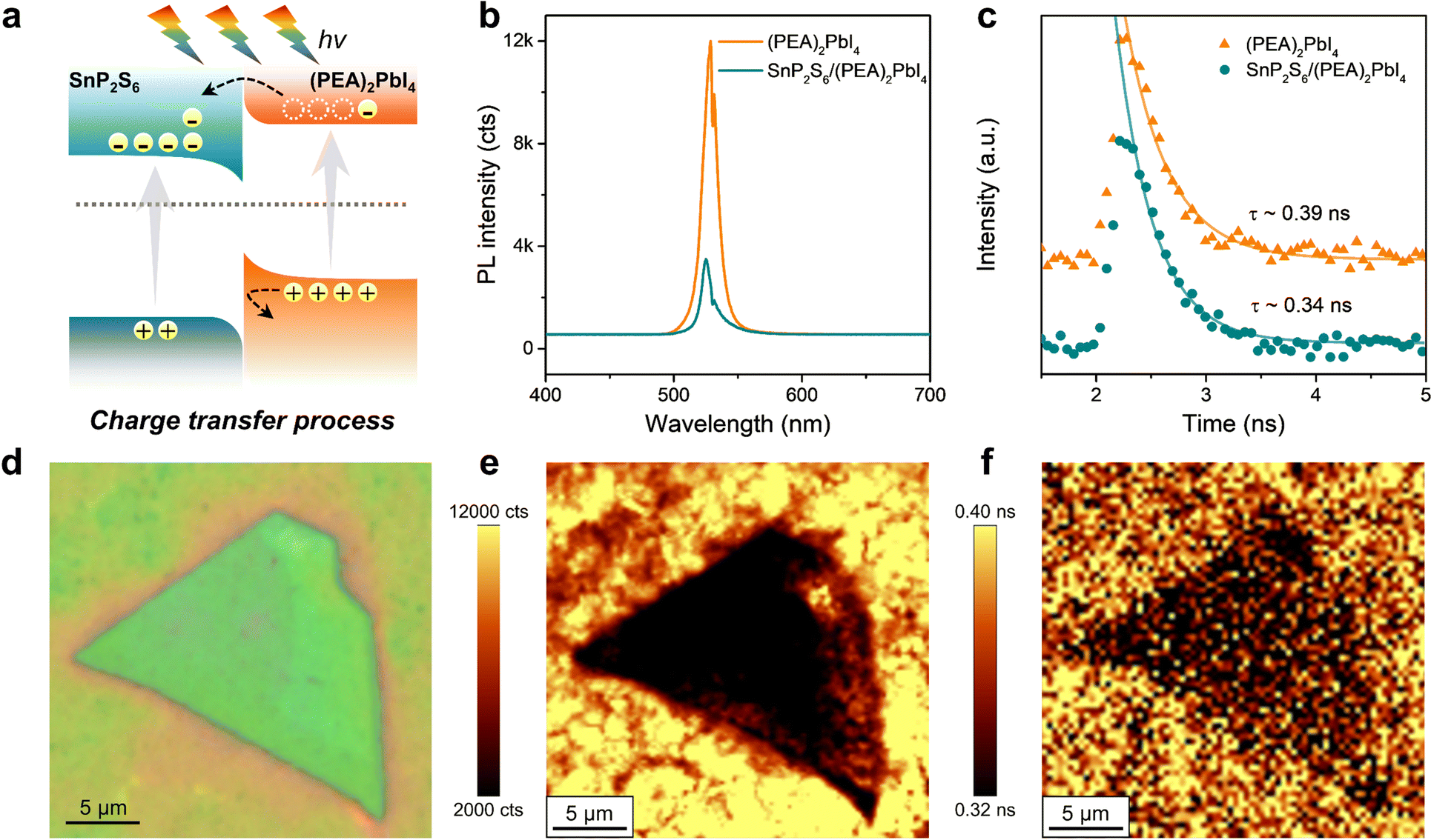 | ||
| Fig. 2 Charge transfer behavior of the SnP2S6/(PEA)2PbI4 heterojunction. (a) Schematic diagram of the charge transfer process of the SnP2S6/(PEA)2PbI4 heterojunction under the illumination condition. (b) Steady-state PL spectra and (c) fluorescence lifetime of (PEA)2PbI4 and the heterojunction. (d) Optical image of the SnP2S6/(PEA)2PbI4 heterojunction. (e) PL intensity mapping and (f) fluorescence lifetime mapping of (d). | ||
Fig. 3a presents the schematic diagram of the SnP2S6/(PEA)2PbI4 heterojunction photodetector with Cr/Au (10/50 nm) as electrodes, and the detailed preparation process can be seen in the experimental section. To evaluate the optoelectronic performance of the heterojunction, the photodetectors based on SnP2S6 and (PEA)2PbI4 have also been prepared for comparison (Fig. S3, ESI†). Here, the light activated area S of the three devices is about 12 μm2, and the thickness of the SnP2S6 flake and the (PEA)2PbI4 layer is about 18 nm and 60 nm, respectively. The current–voltage (Ids–Vds) characteristics of the three devices under dark and illumination conditions are shown in Fig. 3b. The dark current (Idark) of the heterojunction device is higher than that of both SnP2S6 and (PEA)2PbI4 devices, which is consistent with the findings in MoS2/CsPbBr3 and WSe2/CH3NH3PbI2.26,35 Herein, the (PEA)2PbI4 layer serves the double role of a light harvester and a hole conductor. Under laser illumination, the electron–hole pairs generated in the (PEA)2PbI4 layer would be separated driven by the built-in electric field, and the electrons are transferred into the SnP2S6 flake, which would raise the EF of SnP2S6 and lower the EF of (PEA)2PbI4, resulting in the reduction of the Schottky barrier at contacts and the enhancement of the light current (Ilight) of the heterojunction device (Fig. 3f).35Fig. 3c and d presents the spectral response range of the three devices measured at 5 V bias, and the responsivity (R) can be calculated by R = Iph/PS, where Iph = Ilight − Idark refers to the photocurrent, P refers to the power density of the incident laser and S refers to the device effective area.31 Owing to the enhanced absorption and interfacial charge transfer, the photoresponse of the heterojunction device is consistently higher than that of pure SnP2S6 and (PEA)2PbI4 devices. As shown in Fig. 3e, the responsivity of the SnP2S6/(PEA)2PbI4 heterojunction device has been improved by about an order of magnitude compared with that of the pure SnP2S6 device, and a sudden increase at about 520 nm is caused by the complex exciton states in (PEA)2PbI4.36 Besides, the heterojunction device exhibits a high responsivity in the wavelength range of 300–500 nm, followed by a dramatic decrease in the wavelength range of 500–600 nm. Under 400 nm incident laser, the responsivity of the heterojunction device reaches a maximum of 66.4 A W−1, which can be attributed to the stronger absorption at this wavelength.
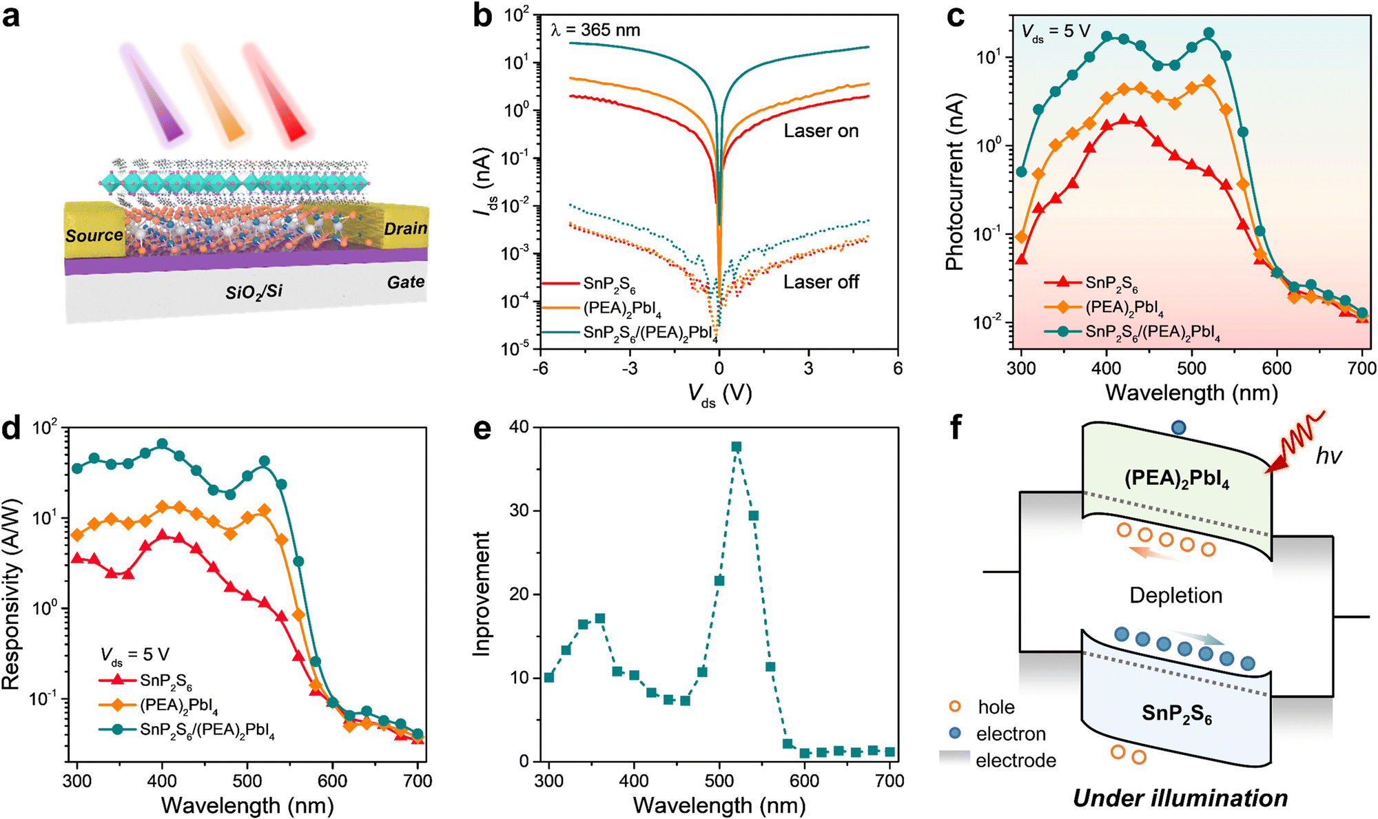 | ||
| Fig. 3 Photodetection performance comparison of the SnP2S6/(PEA)2PbI4 heterojunction with the pristine SnP2S6 flake and the pure perovskite. (a) Schematic diagram of the SnP2S6/(PEA)2PbI4 heterojunction device. (b) Ids–Vds characteristics of SnP2S6, (PEA)2PbI4 and SnP2S6/(PEA)2PbI4 heterojunction devices under dark and illumination conditions. (c and d) Photocurrent and responsivity of SnP2S6, (PEA)2PbI4 and SnP2S6/(PEA)2PbI4 heterojunction devices in the wavelength range of 300–700 nm. (e) Enhanced responsivity of the SnP2S6/(PEA)2PbI4 heterojunction relative to the pristine SnP2S6 flake. (f) Working mechanism of the SnP2S6/(PEA)2PbI4 heterojunction device. | ||
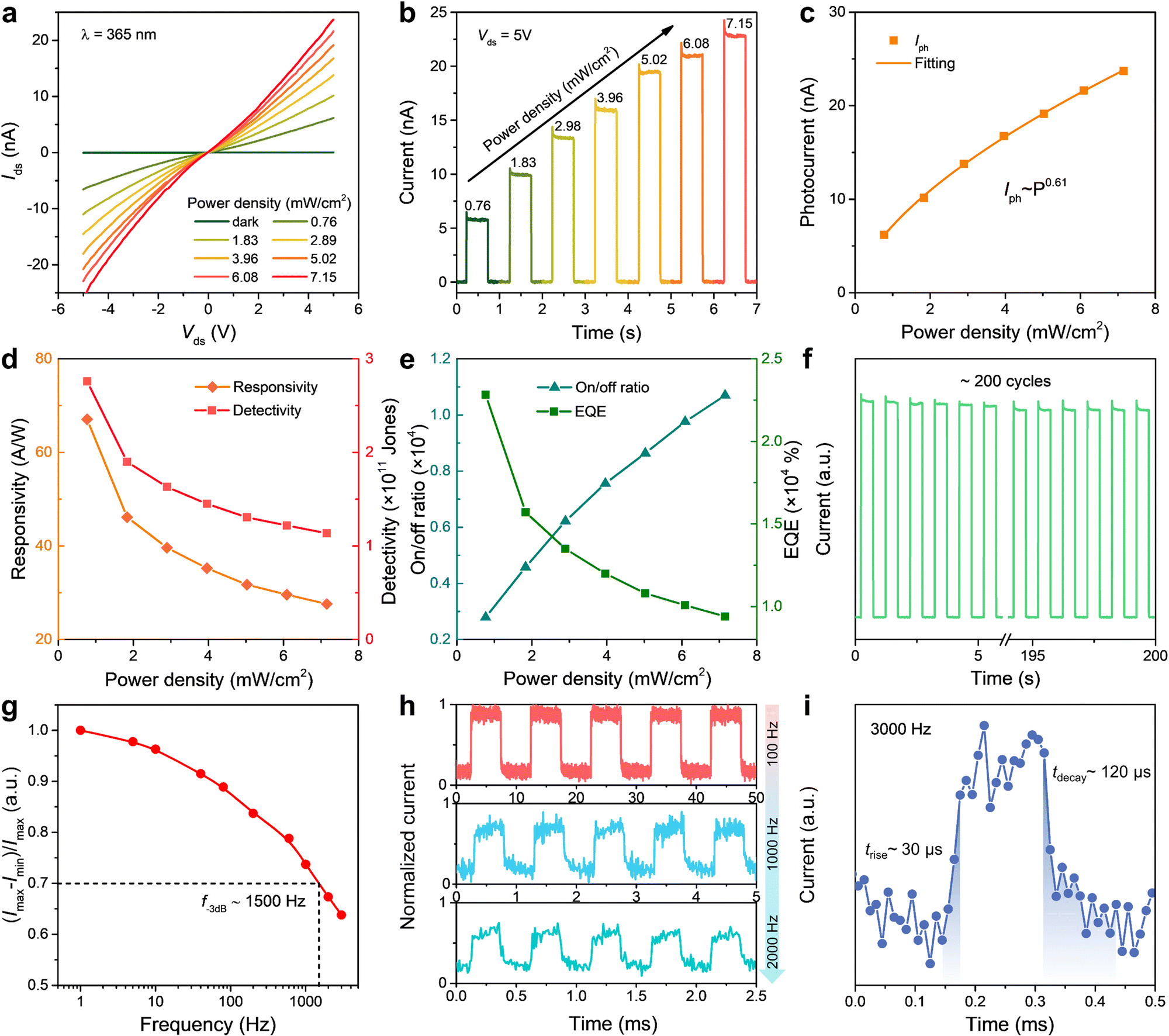
Since the SnP2S6/(PEA)2PbI4 heterojunction device exhibits excellent photoresponse in the UV band, we further systematically evaluated its optoelectronic performance at 365 nm. Fig. 4a and b present the Ids–Vds characteristics and time-resolved photocurrent of the heterojunction device under laser illumination with various densities from 0.76 mW cm−2 to 7.15 mW cm−2. It has been observed that the photocurrent shows a gradually increasing trend as more photo-generated carriers would be excited at stronger laser in the heterojunction.37 Besides, the heterojunction device exhibits excellent on/off switching stability and reversibility. The dependence between photocurrent and laser power density can be fitted by Iph ≈ Pθ.38 As shown in Fig. 4c, the power-law index (θ) of the heterojunction device is 0.61, which deviates from the ideal value (θ = 1). This might be caused by the defect states within the two materials or at their hetero-interface.37 Apart from responsivity, the specific detectivity (D*) is another key parameter to measure the sensitivity of the photodetector, which can be calculated by the equation  (where e represents the elementary charge).39 As shown in Fig. 4d, the responsivity and detectivity of the heterojunction device increase as the laser power density decreases, and the maximum values are up to 67.1 A W−1 and 2.8 × 10¹¹ Jones with a laser power intensity of 0.76 mW cm−2, demonstrating the excellent detection capability for weak light. In addition, the photoelectric performance of pure SnP2S6 and (PEA)2PbI4 devices under 365 nm laser illumination is presented in Fig. S4 (ESI†). Compared with the pure SnP2S6 device (R = 3.1 A W−1, D* = 2.7 × 10¹⁰ Jones, P = 0.76 mW cm−2) and (PEA)2PbI4 device (R = 18.6 A W−1, D* = 8.7 × 10¹⁰ Jones, P = 0.76 mW cm−2), the heterojunction device exhibits higher responsivity and detectivity. The external quantum efficiency (EQE) of the heterojunction device can be calculated by EQE = hcR/e (h, c and λ refer to the Planck constant, speed of light and incident laser wavelength).39 As shown in Fig. 4e, the EQE is as high as 22825% under a laser power density of 0.76 mW cm−2, which confirms the outstanding photoelectric conversion efficiency of the heterojunction device.40 The on/off ratio (Ilight/Idark) of the heterojunction device is calculated to be ∼104, indicating its antinoise ability. Besides, the stability and long-term operability of the heterojunction device confirmed that the photocurrent and dark current of the heterojunction device hardly changed even after about 200 cycles of on/off switching operation (Fig. 4f). To further evaluate the performance stability of the heterojunction device, we also measured its photoresponse curve after 2 weeks storage in the glove box (Fig. S5, ESI†). It can be seen that the heterojunction device still maintains good switching stability but the curve becomes less smooth, which may be attributed to the fact that (PEA)2PbI4 is vulnerable to UV illumination.
 | ||
| Fig. 4 UV detection performance of the SnP2S6/(PEA)2PbI4 heterojunction device. (a) Ids–Vds curves of the device in the dark and under 365 nm laser illumination with various power densities. (b) Time-resolved photoresponse under 365 nm laser illumination with various power densities. (c) The dependence of photocurrent on laser power density at Vds = 5 V. (d and e) Responsivity, detectivity, on/off ratio and EQE as a function of laser power density at Vds = 5 V. (f) Photostability measurement of the device under 365 nm laser illumination with P = 0.76 mW cm−2 and Vds = 5 V. (g) The dependence of current decay on pulsed laser frequency at Vds = 5 V. (h) Photoresponse of the SnP2S6/(PEA)2PbI4 heterojunction device under a 365 nm pulsed laser with various frequencies. (i) Response time of the device under a 365 nm pulsed laser with a frequency of 3000 Hz. | ||
Generally, the response speed determines the capability of the photodetector to detect the rapid change of the optical signals. Therefore, we further investigated the response characteristics of the heterojunction device to a pulsed laser with various frequencies. It can be seen from Fig. 4h that the heterojunction device exhibits stable and reversible response to a pulsed laser with a frequency of 100 Hz, 1000 Hz and 2000 Hz, and its photocurrent remains above 50% of the initial value even under a 2000 Hz pulsed laser. The relationship between the current delay [(Imax − Imin)/Imax] and the pulsed laser frequency is further extracted in Fig. 4g, and the 3 dB cut-off frequency (the frequency-dependent photocurrent drops to 0.707 of the peak value) of the heterojunction device is estimated to be about 1500 Hz.41 As shown in Fig. 4i, the rise time (τrise) and delay time (τdelay) of the heterojunction device in a complete switching cycle are 30 μs and 120 μs at a 3000 Hz pulsed laser, indicating that it is much faster than the pure SnP2S6 device (Fig. S6, ESI†). The fast photoresponse of the heterojunction device can be attributed to the charge separation at the hetero-interface as well as the efficient charge collection in the bottom SnP2S6 flake.12,13
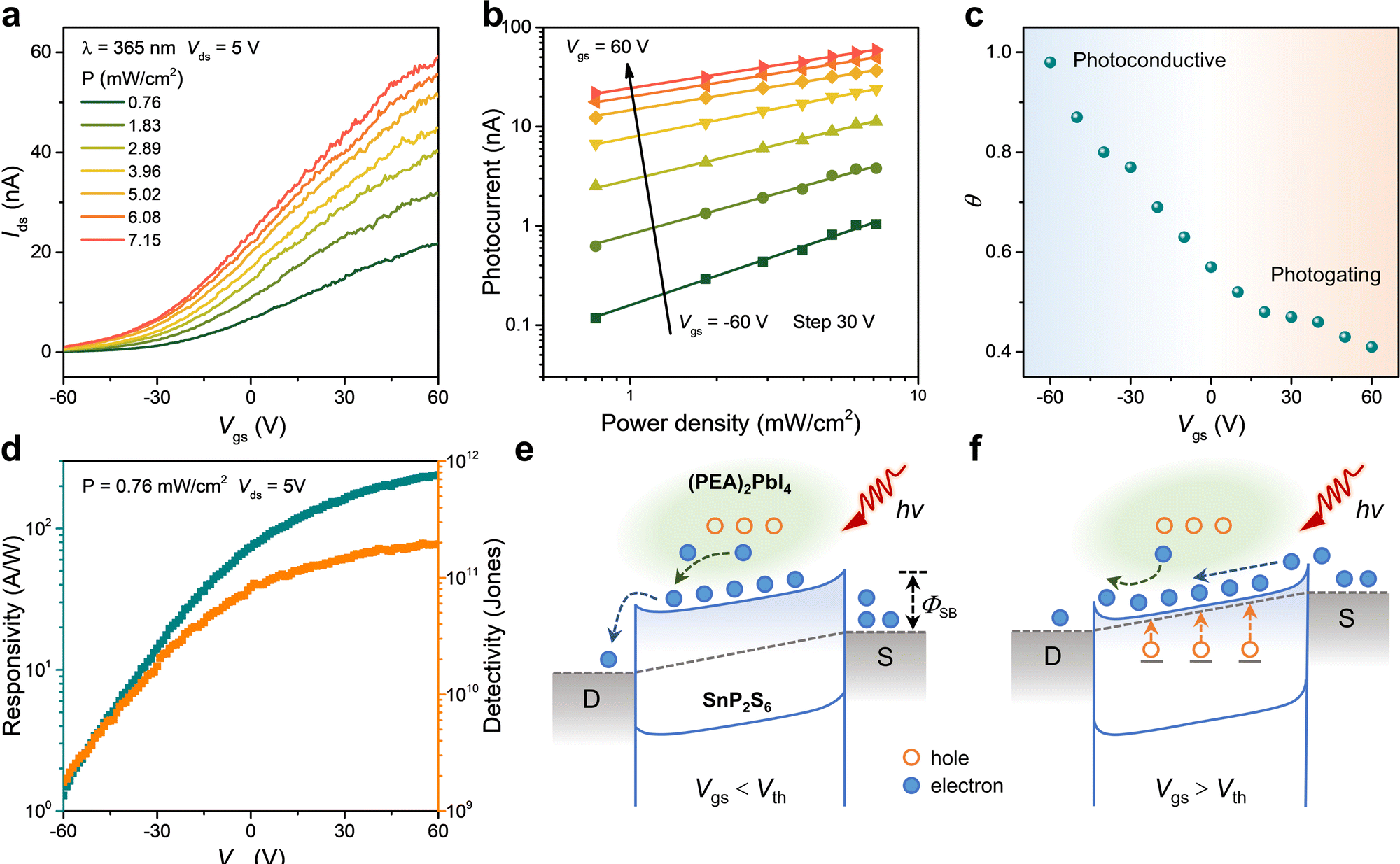
The gate-modulated photoresponse has also been investigated in order to reveal the underlying mechanism of photodetection in the heterojunction device. Fig. 5a presents the transfer characteristic curves of the heterojunction device under 365 nm laser illumination with various power densities, and its transfer characteristic curve under dark conditions is shown in Fig. S7 (ESI†). According to previous reports, the back-gate mainly modulates the Fermi level of n-type SnP2S6 due to the charge screening effect of the SnP2S6 flake underneath, while the top (PEA)2PbI4 layer has not been affected.42,43 Therefore, the heterojunction device exhibits a typical n-type behavior under dark conditions. Under 365 nm laser illumination, the current of the heterojunction device dramatically increases with increasing power density within the gate voltage range from −60 V to 60 V. The dependence between the photocurrent and the laser power density at various gate voltages is shown in Fig. 5b, and the θ values fitted by the power law Iph ≈ Pθ are displayed in Fig. 5c. When the gate voltage varies from −60 V to 60 V, the θ value of the heterojunction device gradually changes from 0.98 to 0.41, indicating the transition of the photocurrent generation mechanism from photoconductive effect (θ = 1) to photogating effect (0 < θ < 1). Such gate-modulated photoresponse behavior has also been reported in hybrid heterojunction devices with a similar structure.44,45 As shown in Fig. 5d, the gate-tunable responsivity and detectivity of the heterojunction device have been demonstrated, which rapidly increase as the gate voltage changes from −60 V to 60 V. This behavior can be explained by the gate-modulated band structure at the SnP2S6–electrode contact interface.33,46 As presented in Fig. 5e, the Fermi level of the SnP2S6 flake underneath moves down and the Schottky barrier at the contact interface significantly increases when Vgs < Vth (Vgs and Vth refer to the gate voltage and threshold voltage, respectively). Right now, the heterojunction device is in the off state, and the channel current is contributed by photo-generated carriers.33,37 In addition, when the heterojunction device is in the on state (Vg > Vth), the Fermi level of the SnP2S6 flake underneath moves towards the conduction band and the Schottky barrier (ΦSB) at the contact interface decreases.37 Therefore, the thermionic and tunneling current gradually increases, resulting in the enhanced channel current (Fig. 5f).47 The synergistic effect of the tunable Schottky barrier and the photogating mechanism can drastically increase the channel current, achieving excellent photodetection performance. Obviously, the responsivity and detectivity of the heterojunction device can reach up to 239.4 A W−1 and 1.9 × 10¹¹ Jones at Vgs = 60 V, respectively.
 | ||
| Fig. 5 Gate-modulated UV detection performance of the SnP2S6/(PEA)2PbI4 heterojunction device. (a) Transfer characteristic curves of the device under 365 nm laser illumination with various power densities. (b) The dependence of photocurrent on laser power density at different gate voltages. (c) The extracted θ as a function of gate voltage. (d) Gate-tunable responsivity and detectivity of the device. (e and f) The carrier transport mechanism of the SnP2S6/(PEA)2PbI4 heterojunction device at Vgs < Vth and Vgs > Vth under 365 nm laser illumination. | ||
Due to the fascinating photodetection performance of the heterojunction device, we further investigated its imaging applications.48,49 The schematic diagram of a single-pixel imaging system is shown in Fig. 6a. A black acrylic mask with the imaging target (hollow pattern) is located between the laser and the 2D SnP2S6/(PEA)2PbI4 heterojunction photodetector, which is controlled by two stepping motors (along the X and Y direction respectively) and can be moved continuously line by line. During the imaging process, the photodetector can accurately detect the laser signal passing through the target and generate photocurrent, which can be collected by the computer. Meanwhile, the location information of the imaging target is also recorded by the computer. Finally, the imaging system converts the current signals into a set of gray values and outputs an image. The size of the imaging target is 200 × 100 pixels, and the scan step along the X direction is 10 pixels. The whole imaging process is conducted in the ambient environment. Fig. 6b and c present the imaging results of the heterojunction device under 405 and 520 nm laser illumination, respectively. Benefiting from the high on/off ratio and the fast response speed, the patterns can be clearly distinguished and possess obvious boundaries, indicating the great potential of the 2D SnP2S6/(PEA)2PbI4 heterojunction device in the field of photoelectric imaging.
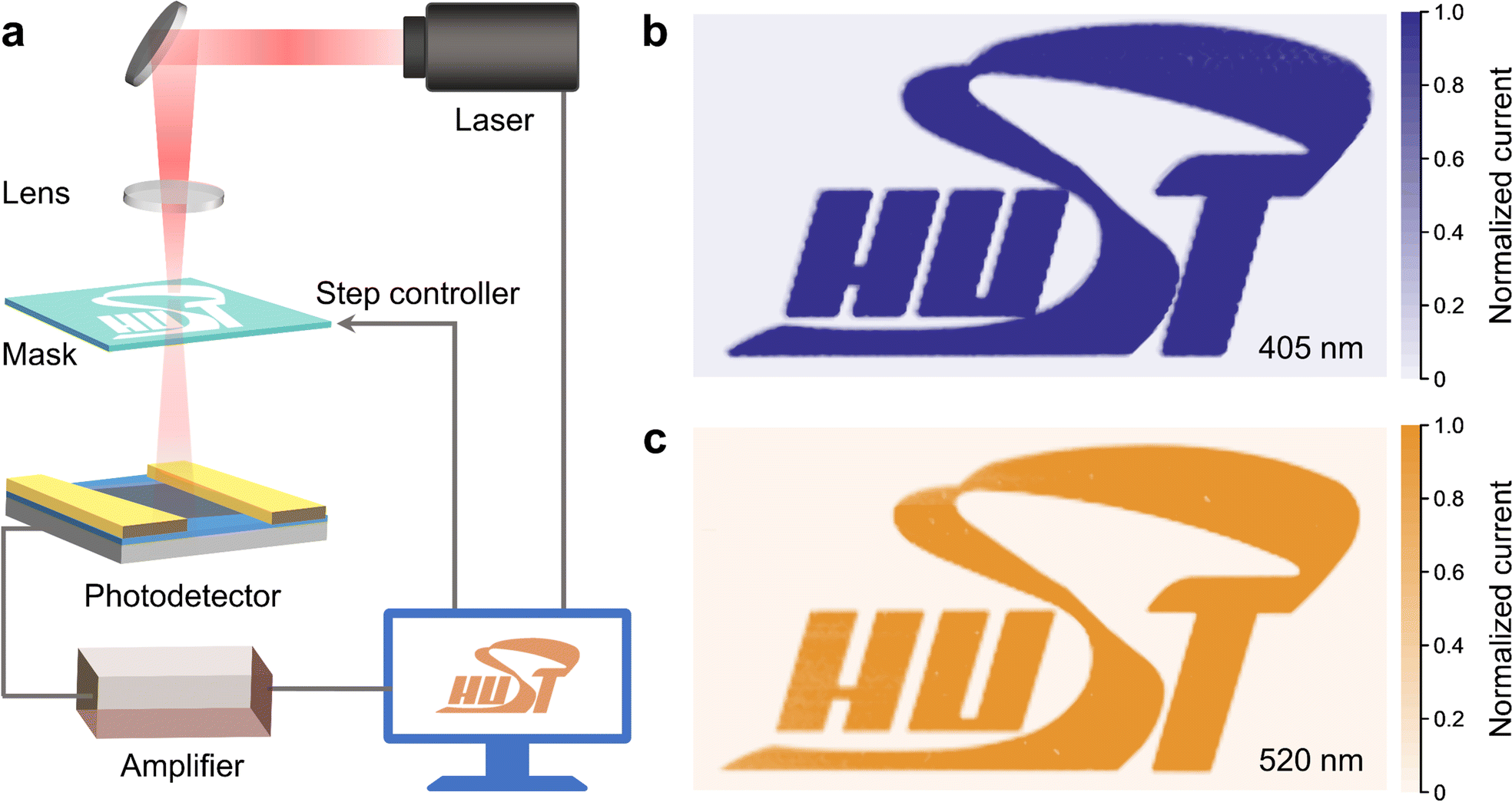 | ||
| Fig. 6 Photocurrent imaging application of the SnP2S6/(PEA)2PbI4 heterojunction device. (a) Schematic diagram of the imaging system. (b and c) Output imaging patterns under 405 and 520 nm laser illumination, respectively. | ||
3. Conclusions
In summary, we have successfully fabricated a 2D SnP2S6/(PEA)2PbI4 hybrid heterojunction for high-performance UV photodetectors by the facile solution spin-coating process. The hybrid heterojunction exhibits significantly enhanced optical absorption in the wavelength range of 300–500 nm, which is attributed to the co-absorption of SnP2S6 and (PEA)2PbI4. Besides, through PL spectra, fluorescence lifetime and UPS measurements, the type-II energy band alignment leading to photocarrier separation and transfer at the SnP2S6 and (PEA)2PbI4 heterojunction interface has been demonstrated. Based on the enhanced absorption and efficient charge transfer, the heterojunction photodetector exhibits a high responsivity of 67.1 A W−1, a large detectivity of 2.8 × 10¹¹ Jones, a fast rise/delay time of 30/120 μs and an excellent external quantum efficiency of 22825% under 365 nm laser illumination. Compared with the pure SnP2S6 device, the responsivity of the hybrid heterojunction device is improved by about 20 times and the response time is improved by 50 times. Due to the synergistic modulation of the photogating effect and Schottky barriers by gate voltage, the responsivity of the heterojunction device can be optimized to 239.4 A W−1. Further, the excellent imaging capability of the heterojunction device has also been demonstrated. We envision that the 2D SnP2S6/(PEA)2PbI4 hybrid heterojunction photodetector presented in this work lays the foundation for the design and implementation of high-performance UV photodetectors.4. Experimental section
4.1 Preparation of 2D SnP2S6 flakes
At first, SnP2S6 single crystals were synthesized by a chemical vapor transport (CVT) method. About a 1 g mixture of Sn, P and S powders with a molar ratio of 1![[thin space (1/6-em)]](https://www.rsc.org/images/entities/char_2009.gif) :2:6 was placed in a vacuum-sealed quartz tube. Then, the quartz tube was put in a dual-temperature zone tubular furnace, and the two ends of the quartz tube were heated to 450 °C (source end) and 400 °C (growth end) within 400 min, respectively. Later, they were kept at the temperature for 7 days, and then naturally cooled to room temperature. After breaking the quartz tube, the SnP2S6 single crystals with high crystallinity can be obtained. Finally, a mechanical exfoliation method was used to prepare the 2D SnP2S6 flakes.
:2:6 was placed in a vacuum-sealed quartz tube. Then, the quartz tube was put in a dual-temperature zone tubular furnace, and the two ends of the quartz tube were heated to 450 °C (source end) and 400 °C (growth end) within 400 min, respectively. Later, they were kept at the temperature for 7 days, and then naturally cooled to room temperature. After breaking the quartz tube, the SnP2S6 single crystals with high crystallinity can be obtained. Finally, a mechanical exfoliation method was used to prepare the 2D SnP2S6 flakes.
4.2 Preparation of (PEA)2PbI4 solution
In our study, 2 mmol of PEAI powder and 1 mmol of PbI2 powder were mixed and dissolved in 4 mL of N,N-dimethylformamide (DMF) solution. Then the solution was heated and stirred at 70 °C for at least 120 min to ensure the complete dissolution of the two powders. It should be noted that the prepared (PEA)2PbI4 solution is stored in a glove box to prevent deterioration.4.3 Fabrication of the SnP2S6/(PEA)2PbI4 hybrid heterojunction device
At first, the 300 nm SiO2/Si substrate used in this study needs to be treated by O2 plasma (10 sccm, 20 min, 50% power) to ensure the smooth process of the subsequent perovskite spin-coating. The 2D SnP2S6 flakes were exfoliated onto the treated substrate, followed by standard electron beam lithography (EBL) and thermal evaporation of 10/50 nm Cr/Au electrodes. Then, 20 μL of (PEA)2PbI4 solution was spin-coated on the as-fabricated SnP2S6 device with 3000 rpm spin speed for 60 s. After spin-coating the (PEA)2PbI4 layer, the device was annealed at 80 °C for 10 min to obtain the SnP2S6/(PEA)2PbI4 hybrid heterojunction. All the fabrication processes involving the perovskite were conducted in a glove box.4.4 Characterization
The morphology and structure of the as-prepared SnP2S6 flake, (PEA)2PbI4 perovskite and SnP2S6/(PEA)2PbI4 heterojunction were characterized by atomic force microscopy (AFM, Dimension Icon, Bruker), scanning electron microscopy (SEM, Quanta 650, FEI), transmission electron microscopy (TEM, Tecnai G2 F30, FEI) and X-ray diffractometry (XRD, D2 Phaser, Bruker). The energy band alignment of the SnP2S6 flake, (PEA)2PbI4 perovskite and SnP2S6/(PEA)2PbI4 heterojunction was measured by ultraviolet photoelectron spectroscopy (UPS, Axis Ultra DLD, Kratos). Besides, the photoluminescence spectra were collected by using a confocal microscope (Alpha 300R, WITec) equipped with a 532 nm laser. And the optical absorption spectra were investigated by using an ultraviolet visible near-infrared spectrophotometer (SolidSpec-3700, SHIMADZU). The photoelectronic measurements of the SnP2S6 flake, (PEA)2PbI4 perovskite and SnP2S6/(PEA)2PbI4 heterojunction were performed in a probe station (TTPX, Lakeshore), which was connected with a semiconductor analyzer (B1500A, Agilent). The power-tunable 365 and 532 nm lasers were used as illumination sources to explore the photoresponse of the devices.Conflicts of interest
There are no conflicts to declare.Acknowledgements
This work was supported by the National Natural Science Foundation of China (21825103, U21A2069). We also acknowledge the technical support from the Analytical and Testing Center in Huazhong University of Science and Technology.Notes and references
- M. Long, Z. Shen, R. Wang, Q. Dong, Z. Liu, X. Hu, J. Hou, Y. Lu, F. Wang, D. Zhao, F. Ding, Y. Tu, T. Han, F. Li, Z. Zhang, X. Hou, S. Wang and L. Shan, Adv. Funct. Mater., 2022, 32, 2204230 CrossRef CAS.
- D. Wu, M. Xu, L. Zeng, Z. Shi, Y. Tian, X. J. Li, C. X. Shan and J. Jie, ACS Nano, 2022, 16, 5545–5555 CrossRef CAS PubMed.
- S. Li, Y. Zhang, W. Yang, H. Liu and X. Fang, Adv. Mater., 2020, 32, 1905443 CrossRef CAS PubMed.
- M. Tian, L. Xu, H. Dan and Y. Yang, Nanoscale Horiz., 2022, 7, 1240–1249 RSC.
- M. A. Susner, M. Chyasnavichyus, M. A. McGuire, P. Ganesh and P. Maksymovych, Adv. Mater., 2017, 29, 1602852 CrossRef PubMed.
- F. Wang, T. A. Shifa, P. Yu, P. He, Y. Liu, F. Wang, Z. Wang, X. Zhan, X. Lou, F. Xia and J. He, Adv. Funct. Mater., 2018, 28, 1802151 CrossRef.
- A. K. Budniak, N. A. Killilea, S. J. Zelewski, M. Sytnyk, Y. Kauffmann, Y. Amouyal, R. Kudrawiec, W. Heiss and E. Lifshitz, Small, 2020, 16, 1905924 CrossRef CAS PubMed.
- J. Chu, F. Wang, L. Yin, L. Lei, C. Yan, F. Wang, Y. Wen, Z. Wang, C. Jiang, L. Feng, J. Xiong, Y. Li and J. He, Adv. Funct. Mater., 2017, 27, 1701342 CrossRef.
- Y. Yan, J. Yang, J. Du, X. Zhang, Y. Y. Liu, C. Xia and Z. Wei, Adv. Mater., 2021, 33, 2008761 CrossRef CAS PubMed.
- J. Duan, P. Chava, M. Ghorbani-Asl, Y. Lu, D. Erb, L. Hu, A. Echresh, L. Rebohle, A. Erbe, A. V. Krasheninnikov, M. Helm, Y. J. Zeng, S. Zhou and S. Prucnal, ACS Appl. Mater. Interfaces, 2022, 14, 11927–11936 CrossRef CAS PubMed.
- X. Han, P. Song, J. Xing, Z. Chen, D. Li, G. Xu, X. Zhao, F. Ma, D. Rong, Y. Shi, M. R. Islam, K. Liu and Y. Huang, ACS Appl. Mater. Interfaces, 2021, 13, 2836–2844 CrossRef CAS PubMed.
- J. Han, F. Wang, S. Han, W. Deng, X. Du, H. Yu, J. Gou, Q. J. Wang and J. Wang, Adv. Funct. Mater., 2022, 32, 2205150 CrossRef CAS.
- M. Peng, Y. Ma, L. Zhang, S. Cong, X. Hong, Y. Gu, Y. Kuang, Y. Liu, Z. Wen and X. Sun, Adv. Funct. Mater., 2021, 31, 2105051 CrossRef CAS.
- Z. Zhang, S. Wang, X. Liu, Y. Chen, C. Su, Z. Tang, Y. Li and G. Xing, Small Methods, 2021, 5, 2000937 CrossRef CAS PubMed.
- H. Wang, Z. Li, D. Li, P. Chen, L. Pi, X. Zhou and T. Zhai, Adv. Funct. Mater., 2021, 31, 2103106 CrossRef CAS.
- W. Wen, W. Zhang, X. Wang, Q. Feng, Z. Liu and T. Yu, Small, 2021, 17, 2102461 CrossRef CAS PubMed.
- C. Song, H. Yang, F. Liu and G. J. Cheng, Nat. Commun., 2021, 12, 4879 CrossRef CAS PubMed.
- Y. Chen, Z. Liu, J. Li, X. Cheng, J. Ma, H. Wang and D. Li, ACS Nano, 2020, 14, 10258–10264 CrossRef CAS PubMed.
- H. Zhou, H. Lai, X. Sun, N. Zhang, Y. Wang, P. Liu, Y. Zhou and W. Xie, ACS Appl. Mater. Interfaces, 2022, 14, 3356–3362 CrossRef CAS PubMed.
- H. Wang, X. Wang, Y. Chen, S. Zhang, W. Jiang, X. Zhang, J. Qin, J. Wang, X. Li, Y. Pan, F. Liu, Z. Shi, H. Zhang, L. Tu, H. Wang, H. Long, D. Li, T. Lin, J. Wang, Y. Zhan, H. Shen, X. Meng and J. Chu, Adv. Opt. Mater., 2020, 8, 1901402 CrossRef CAS.
- Y. Zhang, F. Wang, X. Feng, Z. Zhang, K. Liu, F. Xia, W. Liang, X. Hu, Y. Ma, H. Li, G. Xing and T. Zhai, Adv. Funct. Mater., 2022, 32, 2205757 CrossRef CAS.
- Y. Liu, H. Ye, Y. Zhang, K. Zhao, Z. Yang, Y. Yuan, H. Wu, G. Zhao, Z. Yang, J. Tang, Z. Xu and S. Liu, Matter, 2019, 1, 465–480 CrossRef.
- Q. Liang, Y. Zheng, C. Du, Y. Luo, J. Zhao, H. Ren, J. Xu and Q. Yan, ACS Nano, 2018, 12, 12902–12911 CrossRef CAS PubMed.
- I. P. Studenyak, V. V. Mitrovcij, G. S. Kovacs, O. A. Mykajlo, M. I. Gurzan and Y. M. Vysochanskii, Ferroelectrics, 2001, 254, 295–310 CrossRef CAS.
- H. Li, J. Song, W. Pan, D. Xu, W. A. Zhu, H. Wei and B. Yang, Adv. Mater., 2020, 32, 2003790 CrossRef CAS.
- X. Song, X. Liu, D. Yu, C. Huo, J. Ji, X. Li, S. Zhang, Y. Zou, G. Zhu, Y. Wang, M. Wu, A. Xie and H. Zeng, ACS Appl. Mater. Interfaces, 2018, 10, 2801–2809 CrossRef CAS.
- Y. Tu, Y. Xu, J. Li, Q. Hao, X. Liu, D. Qi, C. Bao, T. He, F. Gao and W. Zhang, Small, 2020, 16, 2005626 CrossRef CAS.
- J. Hu, A. Zheng, E. Pan, J. Chen, R. Bian, J. Li, Q. Liu, G. Cao, P. Meng, X. Jian, A. Molnar, Y. Vysochanskii and F. Liu, J. Mater. Chem. C, 2022, 37, 13753–13761 RSC.
- Y. Liu, C. Lu, M. Luo, T. Han, Y. Ge, W. Dong, X. Xue, Y. Zhou and X. Xu, Nanoscale Horiz., 2022, 7, 1217–1227 RSC.
- H. Wu, Z. Kang, Z. Zhang, Z. Zhang, H. Si, Q. Liao, S. Zhang, J. Wu, X. Zhang and Y. Zhang, Adv. Funct. Mater., 2018, 28, 1802015 CrossRef.
- H. Shang, H. Chen, M. Dai, Y. Hu, F. Gao, H. Yang, B. Xu, S. Zhang, B. Tan, X. Zhang and P. Hu, Nanoscale Horiz., 2020, 5, 564–572 RSC.
- L. Pi, P. Wang, S.-J. Liang, P. Luo, H. Wang, D. Li, Z. Li, P. Chen, X. Zhou, F. Miao and T. Zhai, Nat. Electron., 2022, 5, 248–254 CrossRef CAS.
- H. Wu, H. Si, Z. Zhang, Z. Kang, P. Wu, L. Zhou, S. Zhang, Z. Zhang, Q. Liao and Y. Zhang, Adv. Sci., 2018, 5, 1801219 CrossRef PubMed.
- J. Qiao, F. Feng, S. Song, T. Wang, M. Shen, G. Zhang, X. Yuan and M. G. Somekh, Adv. Funct. Mater., 2021, 32, 2110706 CrossRef.
- C. Ma, Y. Shi, W. Hu, M. H. Chiu, Z. Liu, A. Bera, F. Li, H. Wang, L. J. Li and T. Wu, Adv. Mater., 2016, 28, 3683–3689 CrossRef CAS PubMed.
- H. H. Fang, J. Yang, S. Adjokatse, E. Tekelenburg, M. E. Kamminga, H. Duim, J. Ye, G. R. Blake, J. Even and M. A. Loi, Adv. Funct. Mater., 2019, 30, 1907979 CrossRef.
- F. Wang, J. Wu, Y. Zhang, S. Yang, N. Zhang, H. Li and T. Zhai, Sci. China Mater., 2021, 65, 451–459 CrossRef.
- X. Zhang, X. Liu, C. Zhang, S. Peng, H. Zhou, L. He, J. Gou, X. Wang and J. Wang, ACS Nano, 2022, 16, 4851–4860 CrossRef CAS PubMed.
- H. P. Wang, S. Li, X. Liu, Z. Shi, X. Fang and J. H. He, Adv. Mater., 2021, 33, 2003309 CrossRef CAS PubMed.
- W. Hu, H. Cong, W. Huang, Y. Huang, L. Chen, A. Pan and C. Xue, Light: Sci. Appl., 2019, 8, 106 CrossRef.
- Z. Liu, J. K. El-Demellawi, O. M. Bakr, B. S. Ooi and H. N. Alshareef, ACS Nano, 2022, 16, 7904–7914 CrossRef CAS PubMed.
- N. Huo and G. Konstantatos, Nat. Commun., 2017, 8, 572 CrossRef PubMed.
- A. Castellanos-Gomez, E. Cappelluti, R. Roldan, N. Agrait, F. Guinea and G. Rubio-Bollinger, Adv. Mater., 2013, 25, 899–903 CrossRef CAS PubMed.
- P. Luo, F. Zhuge, F. Wang, L. Lian, K. Liu, J. Zhang and T. Zhai, ACS Nano, 2019, 13, 9028–9037 CrossRef CAS PubMed.
- H. Wu, Z. Kang, Z. Zhang, H. Si, S. Zhang, Z. Zhang, Q. Liao and Y. Zhang, Small Methods, 2019, 3, 1900117 CrossRef.
- K. Liu, B. Jin, W. Han, X. Chen, P. Gong, L. Huang, Y. Zhao, L. Li, S. Yang, X. Hu, J. Duan, L. Liu, F. Wang, F. Zhuge and T. Zhai, Nat. Electron., 2021, 4, 906–913 CrossRef CAS.
- C. Chen, H. Qiao, S. Lin, C. Man Luk, Y. Liu, Z. Xu, J. Song, Y. Xue, D. Li, J. Yuan, W. Yu, C. Pan, S. Ping Lau and Q. Bao, Sci. Rep., 2015, 5, 11830 CrossRef PubMed.
- L. Tong, M. Peng, P. Wu, X. Huang, Z. Li, Z. Peng, R. Lin, Q. Sun, Y. Shen, X. Zhu, P. Wang, J. Xu and L. Ye, Sci. Bull., 2021, 66, 139–146 CrossRef CAS.
- Y. C. Lu, Z. F. Zhang, X. Yang, G. H. He, C. N. Lin, X. X. Chen, J. H. Zang, W. B. Zhao, Y. C. Chen, L. L. Zhang, Y. Z. Li and C. X. Shan, Nano Res., 2022, 15, 7631–7638 CrossRef CAS.
Footnote |
| † Electronic supplementary information (ESI) available. See DOI: https://doi.org/10.1039/d2nh00466f |
| This journal is © The Royal Society of Chemistry 2023 |