
 Open Access Article
 This Open Access Article is licensed under a Creative Commons Attribution-Non Commercial 3.0 Unported Licence
Significant enhancement in the cold emission characteristics of chemically synthesized super-hydrophobic zinc oxide rods by nickel doping
P.
Kumar
a,
M.
Parashar
a,
K.
Chauhan
a,
N.
Chakraborty
b,
S.
Sarkar
b,
A.
Chandra
b,
N. S.
Das
c,
K. K.
Chattopadhyay
b,
A.
Ghoari
d,
A.
Adalder
d,
U. K.
Ghorai
 d,
S.
Saini
e,
D.
Agarwal
e,
S.
Ghosh
e,
P.
Srivastava
e and
D.
Banerjee
*a
d,
S.
Saini
e,
D.
Agarwal
e,
S.
Ghosh
e,
P.
Srivastava
e and
D.
Banerjee
*a
aThin Film and Nanotechnology Laboratory, Faculty of Engineering and Computing Sciences, Teerthanker Mahaveer University, Moradabad, UP 244001, India. E-mail: nilju82@gmail.com
bThin Film and Nanoscience Laboratory, Department of Physics, Jadavpur University, Kolkata, West Bengal 700032, India
cDepartment of Basic Science and Humanities, Techno International Batanagar, Maheshtala, Kolkata 700141, India
dDepartment of Industrial Chemistry, Ramakrishna Mission Vidyamandira, Belur Math, Howrah-711202, India
eDepartment of Physics, Indian Institute of Technology, Hauz Khas South West, Delhi, 110016, India
First published on 30th October 2023
Abstract
The current article presents a huge enhancement in the field emission characteristics of zinc oxide (ZnO) micro/nanorods by nickel doping. The synthesis of pure and nickel-doped zinc oxide (ZnO) micro/nanorods was done by a simple low-temperature chemical method. Both the as-prepared pure and doped samples were analyzed by X-ray diffraction and electron microscopy to confirm the proper phase formation and the developed microstructure. UV-vis transmittance spectra helped in determining the band gap of the samples. Fourier-Transform Infrared Spectroscopy (FTIR) spectra showed the different bonds present in the sample, whereas X-ray Photoelectron Spectroscopy (XPS) confirmed the presence of nickel in the doped sample. Photoluminescence (PL) spectra showed that after doping, the band-to-band transition was affected, whereas defect-induced transition had increased significantly. After the nickel doping, contact angle measurement revealed a significant decrease in the sample's surface energy, leading to a remarkably high water contact angle (within the superhydrophobic region). Simulation through ANSYS suggested that the doped sample has the potential to function as an efficient cold emitter, which was also verified experimentally. The cold emission characteristics of the doped sample showed a significant improvement, with the turn-on field (corresponding to J = 1 μA cm−2) reduced from 5.34 to 2.84 V μm−1. The enhancement factor for the doped sample reached 3426, approximately 1.5 times higher compared to pure ZnO. Efforts have been made to explain the results, given the favorable band bending as well as the increased number of effective emission sites.
1. Introduction
In the modern era of technology, minimizing power consumption for a specific application is always of significant interest. Consequently, the present technological developments are in serious need of harnessing energy. From this point of view, electron field emission (FE) under an applied external electric field, also called cold FE, is a matter of great interest. Cold emission, which is basically a quantum mechanical tunneling phenomenon, requires much less energy for electron ejection compared to conventional thermal emission.1 An ideal cold emitter should have a favorable structure in the nano-regime, with a high aspect ratio. This makes incoming electric flux lines concentrate on the tailored nanostructures, resulting in a huge field enhancement and low turn-on field. Also, the material should have moderate work function values, good electrical conductivity, a favorable band structure, and good thermal stability to withstand the Joule heating effect during cold emission.2–4 Specific nanosystems like carbon nanotubes, graphene, cupric oxide, cadmium sulfide, nickel oxide, tin oxide, and others have shown great potential to be used as cold emitters.5–10 Apart from the materials mentioned above, zinc oxide (ZnO), which is an II–VI semiconductor with a wide and direct band gap of about 3.37 eV (at 300 K) and a large free exciton binding energy of 60 meV,11 has emerged as a novel material for cold emission applications.12–14 Besides its inherent tendency to grow along a particular direction (c axis) that favors efficient cold emission, the material exhibits remarkable thermal stability, favorable mechanical properties, optical gain, and radiation hardness.15–17 Beyond its utility in cold emission applications, the material finds diverse uses in sensors,18 cosmetics,19 solar cells,20 photocatalysts,21 coatings,22 and various other fields.As mentioned earlier, ZnO has the potential to function as a good cold emitter. Thus, this is why there are considerable reports related to the cold emission properties of ZnO. For instance, Q. H. Li et al. reported that tetrapod-like nanostructures are promising candidates for stable FE with a fluctuation of less than 2% even after 72 hours.23 The maximum current density achieved in their work was 18 mA cm−2. A study on the thermo-enhanced FE phenomenon from ZnO nanowires was reported by Zhang et al. They reported that under a constant applied electric field, the field emission current exhibited a nearly hundred-fold increase accompanied by a significant decrease in the turn on field (ETO) as the temperature increased from 323 K to 723 K.24 Y. Lv et al. observed that brush-like ZnO nanowire arrays deposited over carbon cloth offered a remarkably low ETO of 1.02 V μm−1.25 The system also offered an exceptionally high field enhancement factor (β) of 64![[thin space (1/6-em)]](https://www.rsc.org/images/entities/char_2009.gif) 438. In the previous year, J. Singh and A. Srivastava synthesized ZnO nanostructures using the pulsed laser deposition technique. They observed the stable FE characteristics of the aligned ZnO with a low threshold field (ETh) of 2.40 V μm−1.26
438. In the previous year, J. Singh and A. Srivastava synthesized ZnO nanostructures using the pulsed laser deposition technique. They observed the stable FE characteristics of the aligned ZnO with a low threshold field (ETh) of 2.40 V μm−1.26
In the era of nano-science and technology, it is a very common means that the performance of a specific material in a particular field of application is made significantly better by suitable doping, by functionalization or by making suitable hybrids or composites.
Similar instances can also be found in the cold emission application of ZnO. In this regard, the work that addressed the etching of ZnO nanorods by Ar plasma, as reported by Ji et al., is worth mentioning.27 Apart from the Ar treatment, ZnO was also coated with a layer of AlN to achieve favorable band bending. Here, ETO exhibited a remarkable 42% reduction to 6.8 V μm−1, and the hybrid sample reached the highest current density value of 4.1 mA cm−2.
Another report that addressed the FE from graphene-wrapped ZnO came from X. Wang et al. It was shown that the wrapping of the wrinkled graphene structure enhances the FE characteristics of ZnO significantly,28 resulting in ETO and ETh values of 1.63 and 3.12 V μm−1, respectively.
J. Chen et al. employed a similar approach of aluminium doping through electron beam evaporation to enhance the field emission characteristics of ZnO.29 The system gave the best emission characteristics with ETO as low as 6.21 V μm−1 for optimized layer thickness.
Young et al. investigated the field emission properties of hydrothermally synthesized Ag-doped ZnO.30 When the sample was irradiated with UV light, the doped ZnO gave the lowest ETO with a value of 2 V μm−1 associated with a current density of 1 μA cm−2.
An ETO value of 4.7 V μm−1 with a β value of 1686 was obtained from a ZnO rod deposited over silicon pre-patterned by Au.31 In the same study, Lu et al. showed that the screening effect could significantly deteriorate the emission performance of the system. A. Nagar et al. employed the sol–gel method for the synthesis of a ZnO nanostructure.32 It was shown that the geometry of the flower-like structure significantly affects the emission characteristics and related parameters such as current density, ETO, and β.
The synthesis of Al- and Cu-doped ZnO by a hydrothermal method with varying dopant concentrations was reported by Liu et al.33 Both systems offered good FE characteristics. However, the best result with a turn-on field of 1.51, 1.80 V μm−1 from 6% Al- and 4% Cu-doped samples, respectively, was obtained only after wrapping the system with a graphene sheet. S. J. Young and Y. L. Chu developed a system of Pd nanoparticle decorated ZnO quantum dots and quantum wires.34 In their case, including Pd did not have a marked effect in changing the turn-on field, but the decorated system showed more than a 100% increase in the enhancement factor. Jun Chen obtained a very high emission current of 20 mA et al. from their developed system of indium-doped ZnO.35 The high emission current was attributed to the high crystallinity and conductivity of the doped sample.
However, the existing studies, though they sometimes provide good FE results, lack other important features required for proper industry-scale applications.
For instance, Li et al.23 used a high-temperature synthesis process, while Zhang et al.24 needed additional thermal energy to give the best emission result, indicating that the process cannot be considered to be pure tunneling. The method reported by Ye et al. also involves a high-temperature process, and the value of ETO was also quite high.27 The work led by Cao demonstrated that the screening effect could reduce the FE characteristics of ZnO.31 Though this has fundamental importance, it lacks practical application. The work in 34 showed that including Pd did not affect the emission characteristics much. Though doped ZnO gives a very interesting and useful FE result, it has the same drawback with a high thermal energy required in the synthesis process.35
It is also rather surprising that even after the prediction of ANSYS-based simulation regarding the good potential of nickel-doped ZnO as a field emitter, there are a negligible number of reports regarding the same. Only Chang et al. developed Ni-doped ZnO by a thermal evaporation process, which is a high-temperature synthesis approach. For the optimized system, the required temperature was as high as 1100 °C.36 Their as-grown different nanostructure was able to give moderately good FE characteristics and offered a turn-on field of around 1.53 V μm−1, which is rather low compared to the present work. But it is also to be noted that they have defined the turn-on field at a current density value of 0.1 μA cm−2, which is 10 times inferior compared to the present work.
In 2014, Rana et al. reported on the cold emission of Ni-doped ZnO prepared by the wet chemical method. However, they achieved only an 8% reduction of the turn-on field in their 5% Ni-doped ZnO.37 Also, the article remained almost silent regarding the interaction between the sample and water, where excess hydrophilicity of any electronic components is a considerable problem.
Keeping this in mind, the present work deals with the synthesis of ZnO nanorods (ZnO NR) by a KMnO4 seeding-mediated wet chemical route and doping it with transition metal elements like nickel. The as-prepared pure and hybrid samples were characterized by various sophisticated techniques to confirm their phase, microstructure, doping, and bonding information. It is shown that both the samples are well luminescent with emission wavelengths lying in the blue/cyan range. It is also seen that after doping, the characteristics of the sample readily switch over from hydrophilic to superhydrophobic, and the cold emission characteristics are drastically enhanced, with ET and β undergoing a huge enhancement of 2 and 48 times, respectively. As far as the authors are concerned, this is the first report of a superhydrophobic Ni-doped ZnO-based cold emitter. The enhancement has been explained in terms of field enhancement on the favorable nanostructure, favorable band bending, and an increased number of defects that come from oxygen vacancies created after Ni doping.
The current article is expected to be a valuable addition to the related literature.
2. Experimental and characterization
The synthesis of pure and doped ZNR on clean glass and silicon substrates was done by a simple chemical method assisted with KMnO4 pre-seeding.38 In a typical experiment, the KMnO4 seeding was done by taking 0.04 g of KMnO4 in 50 ml of deionized (DI) water and stirring after adding the correct amount of n-hexanol. The system was heated at 80 °C for half an hour. The substrates thus activated were cleaned with DI water and finally dried overnight at 50 °C. After successfully seeding the substrates, they were immersed in a solution prepared by dissolving a certain amount of zinc acetate into DI water. A few pieces of zinc foil were also immersed with the substrates to get a faster reaction. To this solution, NH4OH (25 volume%) was dropwise added under constant stirring till the solution got completely transparent. The system was kept undisturbed for 8 hours. The final sample was obtained only after taking out the substrate covered with white precipitation, washing thoroughly with DI water, and drying overnight. To prepare the Ni-doped sample, a certain amount of (5 at%) nickel nitrate was added to the zinc acetate solution, and the entire process was repeated.The pure and doped samples were named sample A and B, respectively.
The as-prepared pure and doped samples were analyzed by using an X-ray diffractometer (XRD, BRUKER D8 Advance), field emission scanning electron microscope (FESEM, JEOL 6340F FEG-SEM), UV-vis spectrophotometer (Shimadzu UV-3600), Fourier transform infrared spectrometer (Shimadzu IR Affinity-1S FTIR) and photoluminescence spectrophotometer (PL, Shimadzu RF-5301 Spectrofluorophotometer). The surface energy of the samples was calculated by measuring the contact angle of two liquids of known polarity (OCA 15EC, Data Physics). The field emission characteristics of the samples were tested by using a laboratory-assembled field emission setup.
3. Results and discussion
3.1. XRD analysis
The XRD pattern of both samples, A and B, is shown in Fig. 1. The pattern associated with both samples shows a number of strong peaks centered around 2θ = 32.26°, 34.92°, 36.70°, 47.98°, and 57.12°, which correspond to the (100), (002), (101), (102), and (110) crystal planes of the hexagonal wurtzite structure of ZnO, respectively (JCPDS no. 36-1451), with lattice constants a = 3.2554 Å and c = 4.9569 Å.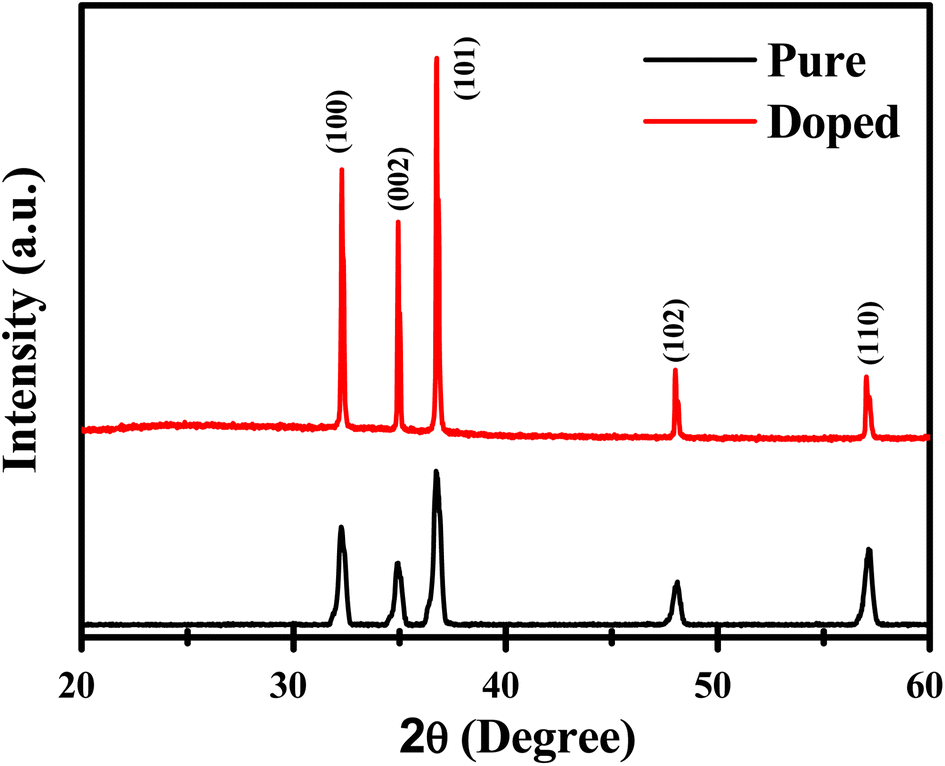 | ||
| Fig. 1 XRD pattern of pure and doped ZnO. | ||
The average crystallite size (D) of the synthesized sample can be calculated using Scherrer's formula as given below:
 | (1) |
3.2. XPS study
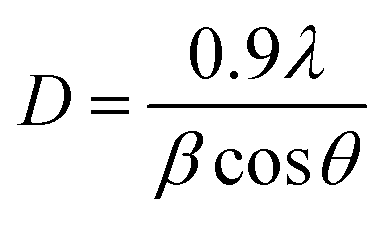
Fig. 2a–d show the XPS spectra of both samples in order to confirm the actual abundance of nickel in sample B and if the inclusion of Ni significantly changes the binding energy of other elements such as Zn and O. The survey spectra (Fig. 2a) show several intense peaks centering around 1044, 1021, 531, 498, 474, 281.6, 138, 87, and 7.47 eV, all of which have been standardized with respect to the C 1s peak located at 281.6 eV. In the spectra of sample B, a very weak peak centered around 860 eV was detected, which is the signature of the Ni 2p level. Due to its weak intensity, a separate high-resolution scan was performed, which is shown in Fig. 2d. The peaks with lower intensity in the lower binding energy region (498, 474, 281.6, 138, 87, and 7.47) are all associated with the Zn 3 level (3s, 3p, and 3d), as assigned in the scan and Zn KLL and LMM levels. The two most intense peaks at 1044 and 1021 eV are the signatures of the Zn 2p level (Zn 2p3/2 and 2p1/2). The high-resolution scans of these two peaks are separately shown in Fig. 2c, and it is seen that, unlike the oxygen 1s state that can be seen in Fig. 2b, the inclusion of Ni does not result in any difference in the Zn 2p level. The O 1s spectra, when deconvoluted, give two peaks centered around 529 and 531 eV, as shown in Fig. 2b. The peak at 529 eV is the characteristic of O2− ions in wurtzite ZnO,39 whereas that at 531 eV confirms the existence of an oxygen-deficient region in ZnO. It is clearly seen that after Ni doping, the peak at 529 eV is very prominent in sample B, and the same result was quantitatively confirmed when the area under the curves was computed from the deconvoluted spectra. The area of the curve centered at 529 eV in sample B is more than twice the same associated with sample A. These defects are likely to play a significant role in the subsequent discussion regarding the photoluminescence (PL) properties of the sample.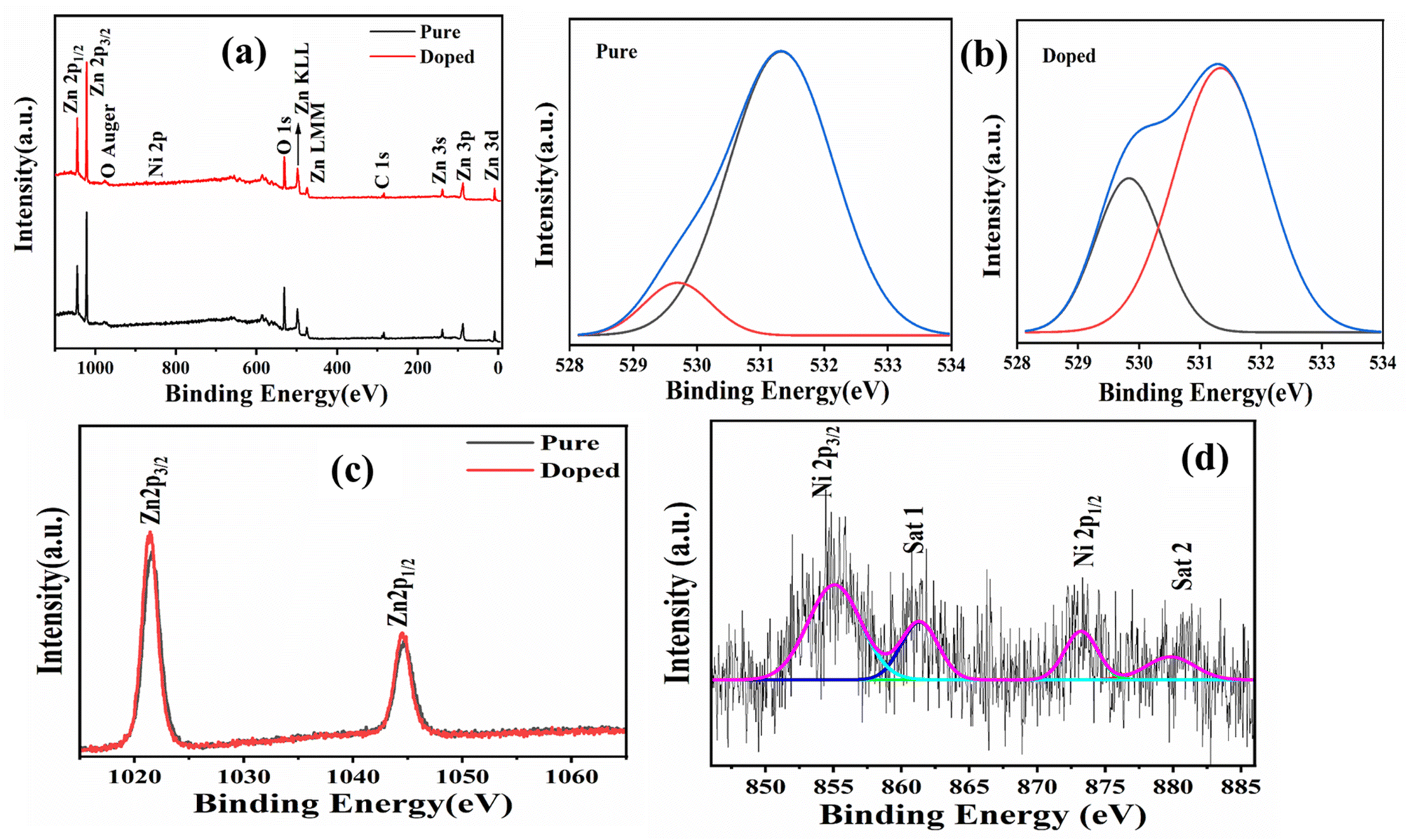 | ||
| Fig. 2 XPS (a) survey scan of (b) O 1s and (c) Zn 2p spectra of both sample A and B; (d) Ni 2p high resolution scan of sample B. | ||
The presence of Ni can clearly be seen in Fig. 2d, where two main peaks centered at 855.29 and 873.46 eV are the signatures of Ni 2p3/2 and 2p1/2 levels. These two peaks are accompanied by two satellite peaks at 861.25 and 879.82 eV.40 These satellite peaks arise due to the difference in the electronic configuration between the ground state and excited state during photoelectron emission. The shakeup lines indicate a charge-transfer transition from O (2p) to Ni (3d), resulting in hybridization.41 When quantification analysis is done, it is revealed that the Ni is present with an atomic percentage of 1.76 and a weight percentage of 4.28. All these together confirm the successful doping of ZnO nanostructures.
3.3. FESEM study
FESEM analysis is a useful technique to investigate the morphology and structure of materials at micro- and nano-scale levels. Fig. 3(a–f) show the FESEM micrographs of both samples with different magnifications. | ||
| Fig. 3 FESEM images of pure (a–c) and doped (d–f) ZnO with different magnifications. | ||
From Fig. 3(a–c), it is seen that one-dimensional structures with a diameter of around 400 nm and length of the order of several micro-meters have been formed uniformly. The hexagonal structures of the individual rod can clearly be seen, with the width of each side lying between 100 and 120 nm.
When ZnO gets doped with Ni, it is seen that (Fig. 3(d–f)) though the structure of the sample was still one dimensional, it undergoes distortion, and 2 D flake-like structures with sharp edges begin to form. These structures are expected to contribute to further field enhancement and better field emission characteristics, which will be discussed in the coming section.
3.4. Optical properties
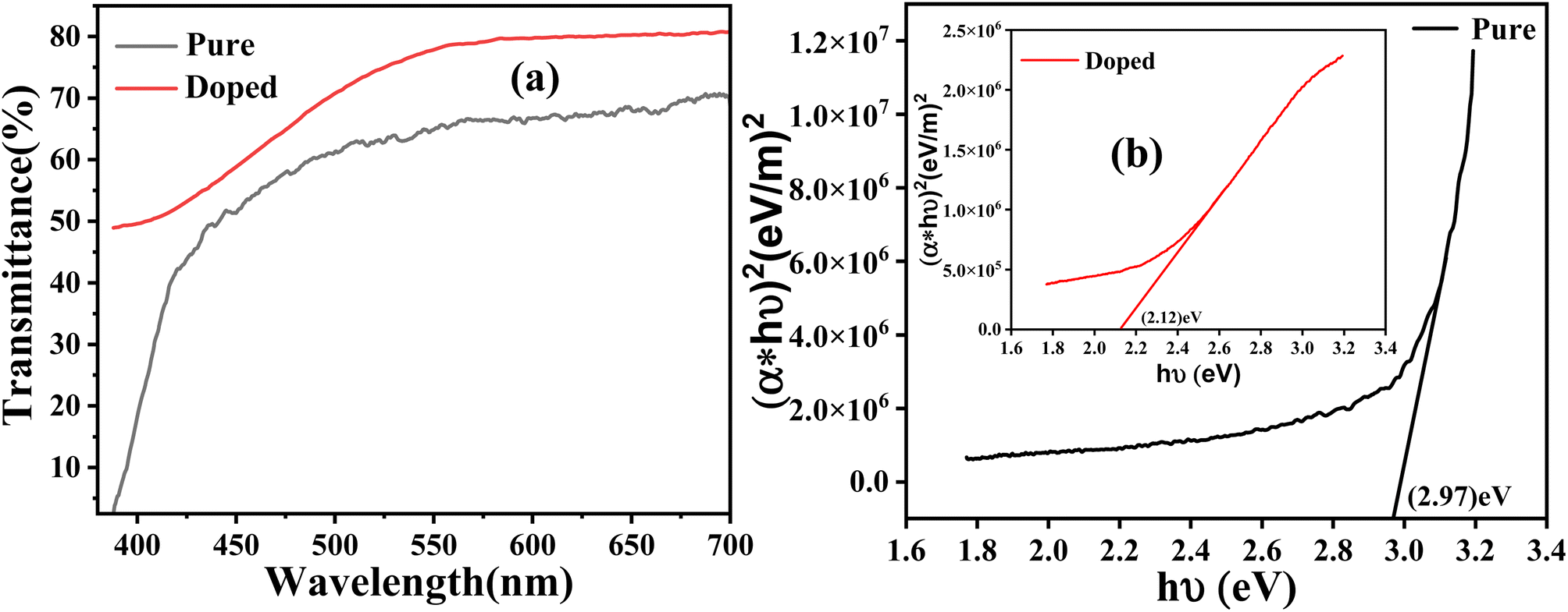 | ||
| Fig. 4 Transmittance spectra (a) and Tauc plot (b) of both the pure and doped samples (inset (b): the Tauc plot of sample B). | ||
The standard Tauc formula is used to calculate the absorption coefficient (α).
 | (2) |
| (αhv)2 = A(hv − Eg) | (3) |
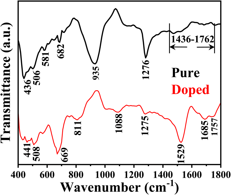 | ||
| Fig. 5 FTIR spectra of both the samples in the lower wavenumber region 400–1800 cm−1. | ||
It is clearly seen that both samples have few peaks common with slight shifting. For instance, the peaks at 436, 506, and 1276 cm−1 shift to 441, 508, and 1275 cm−1 in the case of sample B. Sample A has other prominent peaks at 682 and 935 cm−1 and a band between 1436 and 1762 cm−1. In the case of sample B, the information can be seen at 666, 811, 1088, 1529, 1685, and 1757 cm−1. The band in sample A forms due to the overlapping of different C–H, C–C, and C![[double bond, length as m-dash]](https://www.rsc.org/images/entities/char_e001.gif) O bonds, either absorbed or formed during synthesis on the ZnO surface.42 Of all these, peaks at 436 (or 441) and 506 (or 508) cm−1 are the signatures of the Zn–O stretching bond,43 of which the peak corresponding to 506 cm−1 is Raman active.44 A very strong peak at 935 cm−1 in the case of sample A signifies a considerable number of O–H groups in sample A.45 Thus there is a probability that this OH group could react with external water droplets, forming a hydrogen bond resulting in its hydrophilic nature, which will be discussed in the coming section. The peak at 682 cm−1 in sample A also confirms the presence of a Zn–O bond, which may shift and overlap with the peak at 666 cm−1, as seen in sample B.46 This peak at 666 cm−1, seen in the case of sample B may probably be due to the Ni–O stretching vibrational mode.47 This indirectly confirms the presence of Ni in sample B. The transmittance peak at 1275 cm−1 shown in both samples probably comes from the carbonaceous impurities48 or the Si substrate.49 The peaks at 811, 1685, 1088, 1529, and 1757 cm−1 appear in the spectra of sample B and bear the signatures of C–H out of plane bending, CO stretching C–C/CC stretching, and CO stretching modes.46,50–52
O bonds, either absorbed or formed during synthesis on the ZnO surface.42 Of all these, peaks at 436 (or 441) and 506 (or 508) cm−1 are the signatures of the Zn–O stretching bond,43 of which the peak corresponding to 506 cm−1 is Raman active.44 A very strong peak at 935 cm−1 in the case of sample A signifies a considerable number of O–H groups in sample A.45 Thus there is a probability that this OH group could react with external water droplets, forming a hydrogen bond resulting in its hydrophilic nature, which will be discussed in the coming section. The peak at 682 cm−1 in sample A also confirms the presence of a Zn–O bond, which may shift and overlap with the peak at 666 cm−1, as seen in sample B.46 This peak at 666 cm−1, seen in the case of sample B may probably be due to the Ni–O stretching vibrational mode.47 This indirectly confirms the presence of Ni in sample B. The transmittance peak at 1275 cm−1 shown in both samples probably comes from the carbonaceous impurities48 or the Si substrate.49 The peaks at 811, 1685, 1088, 1529, and 1757 cm−1 appear in the spectra of sample B and bear the signatures of C–H out of plane bending, CO stretching C–C/CC stretching, and CO stretching modes.46,50–52
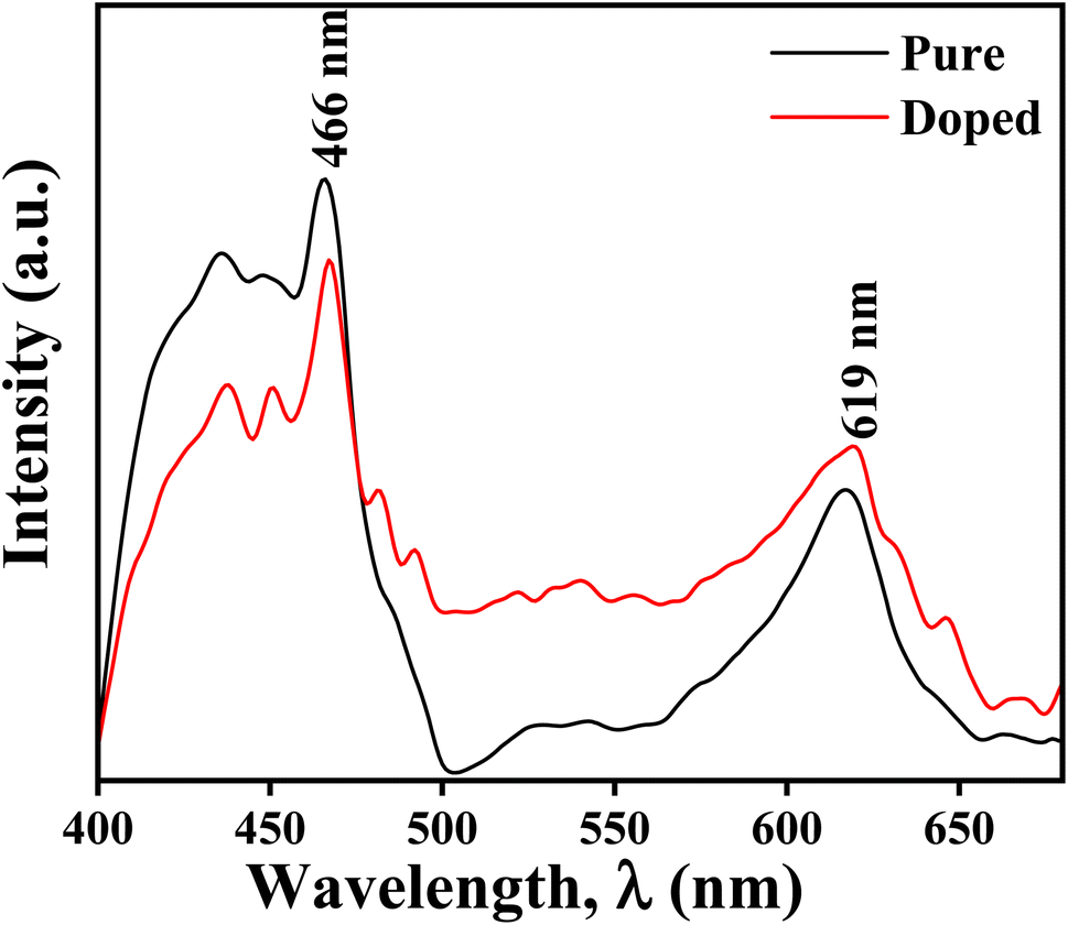 | ||
| Fig. 6 Photoluminescence spectra of both the pure and doped samples. | ||
Regarding the second peak sample A has an intensity not as high as that of sample B, and in the case of sample B, the peak with higher intensity has much higher broadening. Thus the peak basically gets converted to a broad band. This confirms that sample B is much more defect rich, and it would not be wrong to assume that the defect is mainly due to the oxygen vacancy, as confirmed by the XPS study. This has a marked effect on the cold emission characteristics, which will be discussed in the coming section. The CIE chromaticity diagrams for the doped and un-doped samples are shown in Fig. 7a and b. The CIE (x, y) coordinate of sample A is (0.26312, 0.27115), and for B, it is (0.28452, 0.29641). From the chromatography diagram, it is clearly seen that after doping, the emission color moves toward cyan from the blue region.
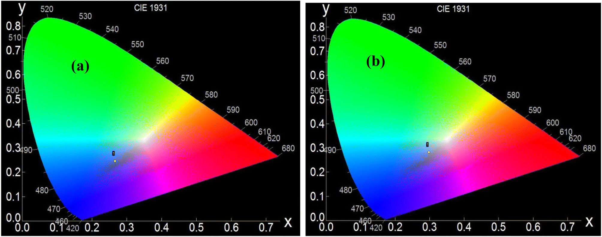 | ||
| Fig. 7 CIE chromaticity diagrams of samples (a) A and (b) B. | ||
3.5. Contact angle measurement and surface energy calculation
The surface energies of both samples were calculated from the contact angle of two liquids, water and glycerol, with known polarity. The response of the sample surfaces toward water and glycerol can be seen in Fig. 8(a–d). It is seen that after doping, the water contact angle increased significantly from 57 to 150°, suggesting a drastic switch from a hydrophilic to a superhydrophobic region. The changes in the relative abundance of the different functional group in the doped sample compared to the pure one may be the key reason for such changes. In Section 3.4.2 while discussing the FTIR spectra it is seen that sample A has a strong FTIR signal at 935 cm−1 associated with the O–H group which disappeared when the sample is doped. This presence of the O–H group facilitates the formation of a hydrogen bond with the external water droplet resulting in hydrophilicity in the corresponding sample.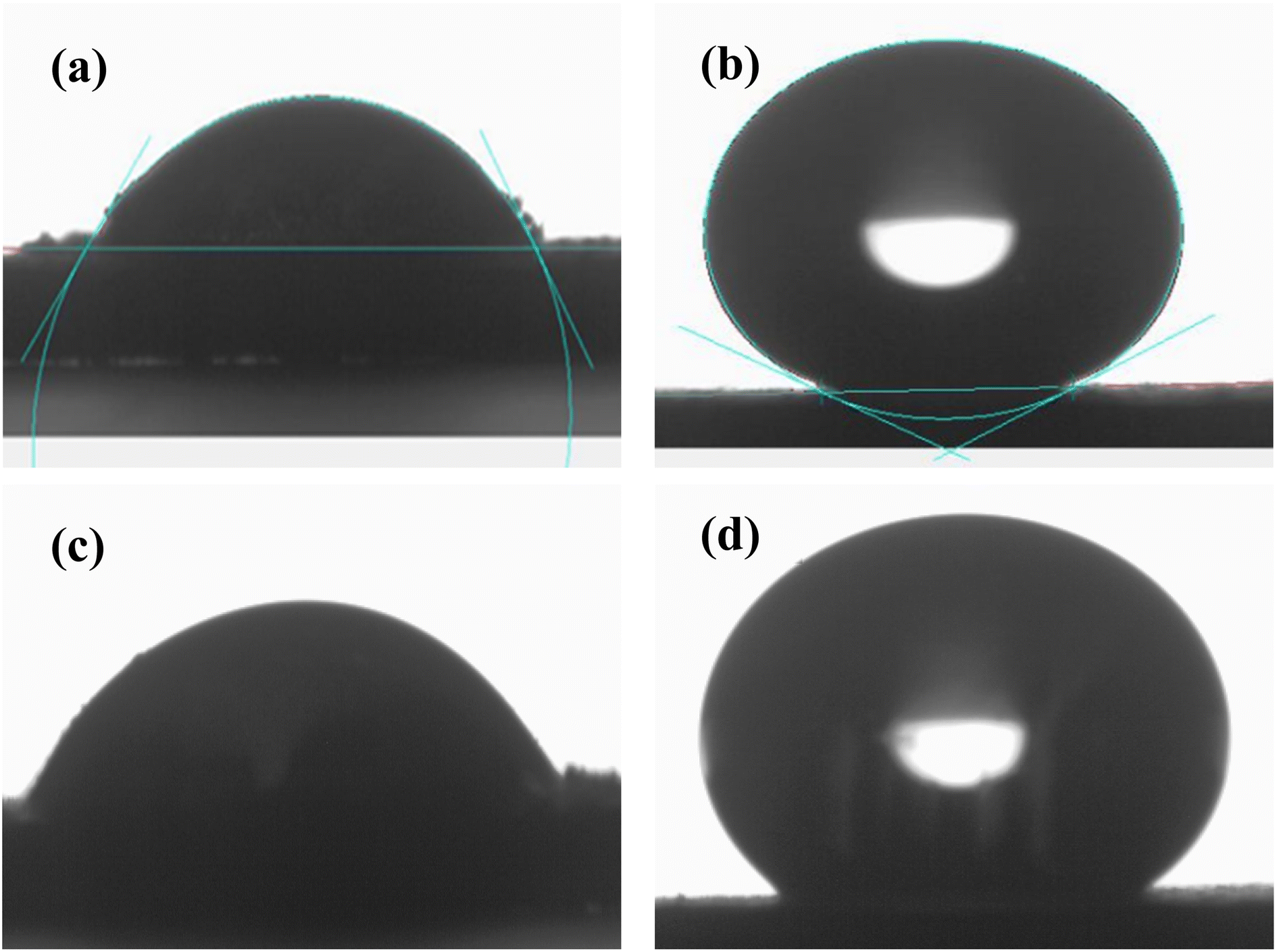 | ||
| Fig. 8 Response of the sample A towards (a) water, (c) glycerol and sample B towards (b) water and (d) glycerol. | ||
Also, the first principles study done by Wang et al.53 in explaining the hydrophobic properties of aluminium doped ZnO can be mentioned here to understand the change in the hydrophobic nature of the sample. Experimentally the group has shown that when pure ZnO is doped with Al the hydrophobicity of the doped sample increased significantly and they claimed that the preferential growth of ZnO crystals can be attributed to the change in the hydrophobic nature of the sample. They have shown that after doping, the intensities of both the XRD peaks associated with (100) and (002) planes increased significantly as in the present case of nickel doped ZnO.
It is reported that in the case of the (002) plane of ZnO, the oxygen atom residing on the surface forms a bond with the hydrogen atom of water with a bond length O(ZnO)–H(H2O) of 1.893 A, and a O(ZnO)–H(H2O)–O(H2O) angle of 172.2°. In contrast, on ZnO (100) surfaces, oxygen of water forms a strong bond with the Zn atom, to gain the minimum energy configuration and the corresponding Zn(ZnO)–O(H2O) distance is 2.094 A with a Zn(ZnO)–O(H2O)–H(H2O, up) angle of 118.0°. The higher bond length and lower bond angle always play an important role in gaining enhanced hydrophobicity. Thus, the relative abundance of these two crystal planes may be the key reasons for such enhanced hydrophobicity (in the present case it is ZnO(100)/ZnO(002) = 1.27 and 1.42 respectively for pure and doped samples) along with the other parameters like changes in microstructures, roughness or porosity. However, these needs further studies to be verified.
These contact angle data can be used to calculate both the polar (Sp) and dispersive (Sd) components of the surface energy using the equation below:54
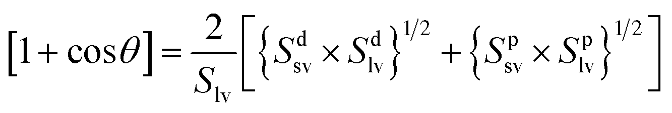 | (4) |
Here, we have taken Splv = 51.0 mJ m−2 and Sdlv = 21.8 mJ m−2 for water and Splv = 30.0 mJ m−2 and Sdlv = 34.0 mJ m−2 for glycerol to calculate the surface energy; all the results have been summarized in Table 1.55 The result shows that the polar part of the surface energy governs the water contact, as reported previously.
| Sample | Contact angle (°) | Surface energy mN m−1 | |||
|---|---|---|---|---|---|
| Water | Glycerol | Polar | Dispersive | Total | |
| A | 57.65 | 41.29 | 15.94 | 34.36 | 50.29 |
| B | 150 | 138.81 | 0.28 | 3.45 | 3.73 |
The primary factor contributing to the reduced water contact angle on surface A, as indicated by the FTIR spectra, could be attributed to the presence of a significant number of OH groups. These groups interact with water by forming unwanted hydrogen bonds resulting in hydrophilicity in this sample.
3.6. Field emission
The capability of cold electron emission by the synthesized nanostructures was theoretically predicted using ANSYS Maxwell software. For this finite array of the samples, both pure and doped ZnO structures were modeled in the software. The dimensions, shapes and morphologies of the nanorod arrays were taken as per the actual experimental findings seen under a FESEM. After the modeling, electrical excitation was virtually applied by the software keeping the range of the excitation voltage as per the actual experimental values. The electrode separation was also fixed as used in the real experimental set-up. The resulting output electric field distribution was plotted using an appropriate color code around the proximity of the simulated sample models along with the field line distribution and shown in Fig. 9a–h. Fig. 9a–d, respectively, show the structure of sample A, incoming electric flux, and ultimate field distribution over the sample.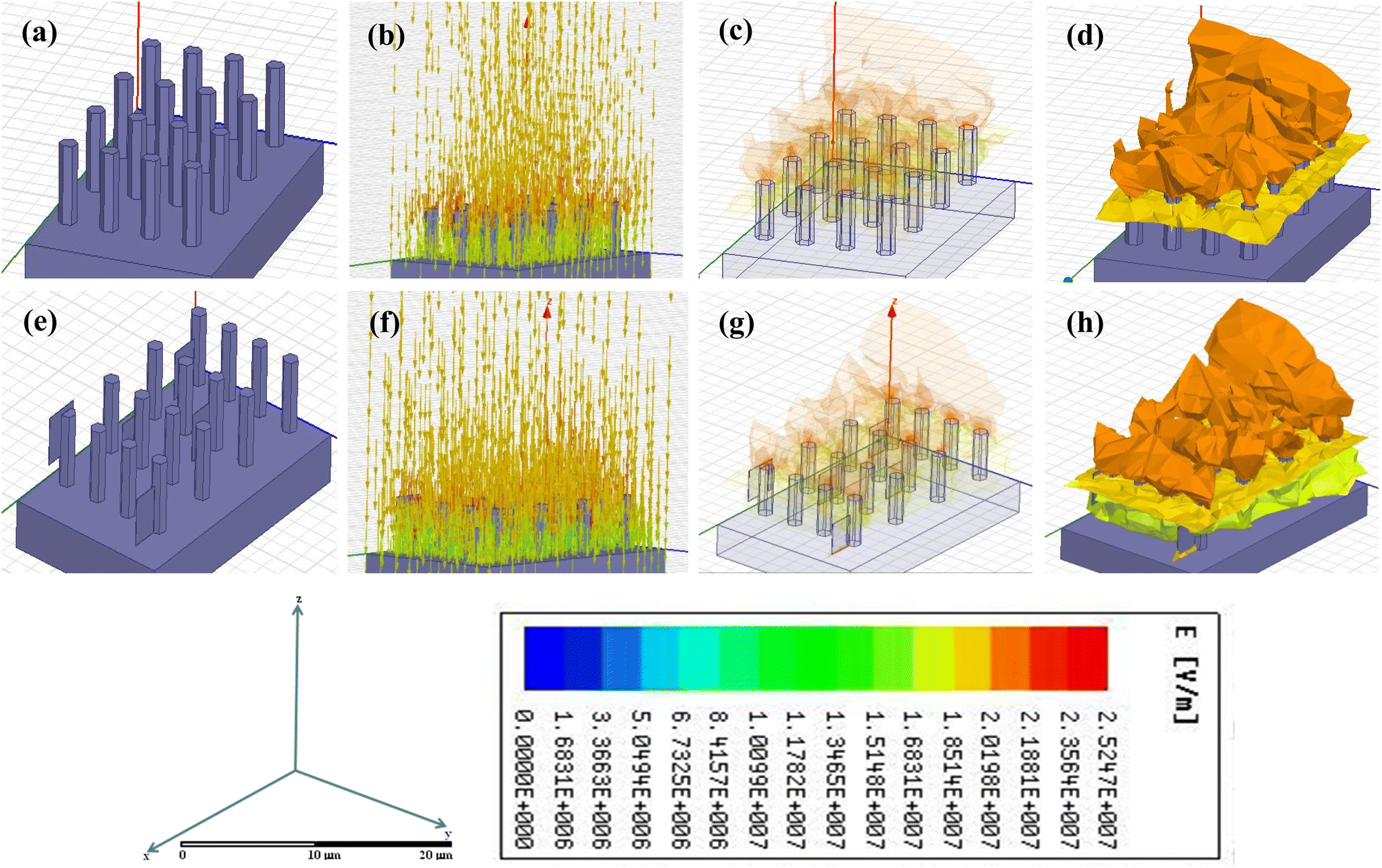 | ||
| Fig. 9 ANSYS field line distribution for the samples (a–d) A and (e–h) B. | ||
Fig. 9e–h show the same parameters for sample B. Fig. 9c, d, g and h are basically the same duo of field line distribution where transparency is introduced only to show the concentration of the field over the sharp tips/edges of the nanostructures.
It is clearly seen that for the doped sample, the intensity of the applied electric field is much higher, and at the same time, the field distribution is much more favorable for the doped sample to function as a cold emitter.
Propelled by the positive theoretical result, FE measurements were carried out using a laboratory-assembled field emission setup. The measurements were carried out using a diode configuration consisting of a cathode (the film under test) and a stainless steel anode mounted on a liquid nitrogen-trapped rotary-diffusion high vacuum chamber with an appropriate chamber baking arrangement. The measurements were performed at a base pressure of ∼10−7 mbar. The inter-electrode distance was kept as high as 300 μm. The macroscopic applied electric field can be obtained by dividing the applied voltage by the inter-electrode distance. Theoretically, the emission current and the macroscopic electric field are related to each other by the well-known Fowler–Nordheim equation56
| I = AatF−2ϕ−1(βE)2exp{−bvFϕ3/2/βE} | (5) |
| ln{J/E2} = ln{tF−2aϕ−1β2} − [{vFbϕ3/2β−1}/E] | (6) |
Hence, the plot of ln {J/E2} vs. 1/E should be a straight line, and its slope and intercept give valuable information about the enhancement factor, local work function, etc. An experimental F–N plot has been modelled, which can be expressed as
| ln{J/E2} = ln{raϕ−1β2} − [{sbϕ3/2β−1}/E] | (7) |
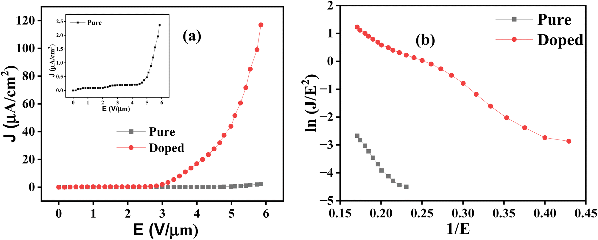 | ||
| Fig. 10 (a) Field emission J–E curves and (b) corresponding F–N plots of pure and hybrid ZnO. | ||
It is seen that the emission current density has a huge enhancement in the case of the doped sample. Also, the turn-on field (ETO), which is defined as the field required to produce a current density of 1 μA cm−2, reduced from 5.34 to 2.84 V μm−1. The value 2.84 V μm−1 may sometimes seem comparable to the reported value, but it is to be kept in mind that the inter-electrode distance is much higher in our case, giving advantages to our cold emitter with respect to other reported work (see Table 3). The straight-line nature of the F–N plot (Fig. 10b) confirms that the electrons are emitted by the process of cold emission and the enhancement factor (β), which can be calculated from the slope (m) of the F–|N plot using the relation m = −bϕ3/2/β and the same plot gives the values of the effective work function (ϕeff) after using the relation ϕeff = ϕ/β2/3. In the calculation, the values of ϕ have been taken as 5.09 and 4.05 eV for pure and Ni-doped ZnO, respectively, following the work reported by C. Chai et al.57 The calculated values of the corresponding parameters are summarized in Table 2.
| Sample | Electrode distance (μm) | E TO (V μm−1) | β | ϕ eff (eV) |
|---|---|---|---|---|
| ZnO | 300 | 5.34 | 2399 | 0.0299 |
| Ni doped ZnO | 300 | 2.84 | 3372 | 0.0190 |
The above results clearly suggest that the doped sample has much better emission characteristics compared to pure ZnO. There are different possible reasons that alone or collectively can explain the significant enhancement of the cold emission characteristics of the doped sample.
Firstly, it is seen that due to Ni doping, there is a change in the morphology of the sample, and unlike in sample A, sample B shows the presence of a few two-dimensional sheet-like structures with sharp edges. These edges have a favorable configuration for the field lines to be concentrated into it and, thus, overall, have a higher enhancement factor. Similar results can be seen in Fig. 9, where the ANSYS-Maxwell simulation clearly shows how the field lines concentrate on sample B much more than sample A.
Defect-induced states also play an important role in monitoring the FE characteristics of a cold emitter. The XPS study shows that Ni-doped ZnO has much a larger number of defects, mainly from oxygen vacancies. In this regard, the work reported by Chen et al.58 showed that ZnO nanowires were synthesized via CVD and subsequently annealed. The as-grown sample were subjected to annealing at a temperature of 800 °C for 60 min, with a constant oxygen flow of 50 sccm. It was seen that when the cold emission characteristics of both the samples were taken, the as-grown sample gave much better emission characteristics compared to the annealed one. It was thereafter concluded that after annealing, the oxygen defect density decreased, resulting in higher resistivity in this sample, which in turn degraded the FE properties of the annealed sample considerably. Therefore, the higher oxygen vacancies in sample B can be another reason for better FE characteristics in such a sample.
The inclusion of Ni on the ZnO lattice results in favorable band bending, as discussed in-depth by Rana et al. in their reported work on the cold emission properties of Ni-doped ZnO.37 Following their explanation, the detailed energy band diagram schematically is shown in Fig. 11a–d.
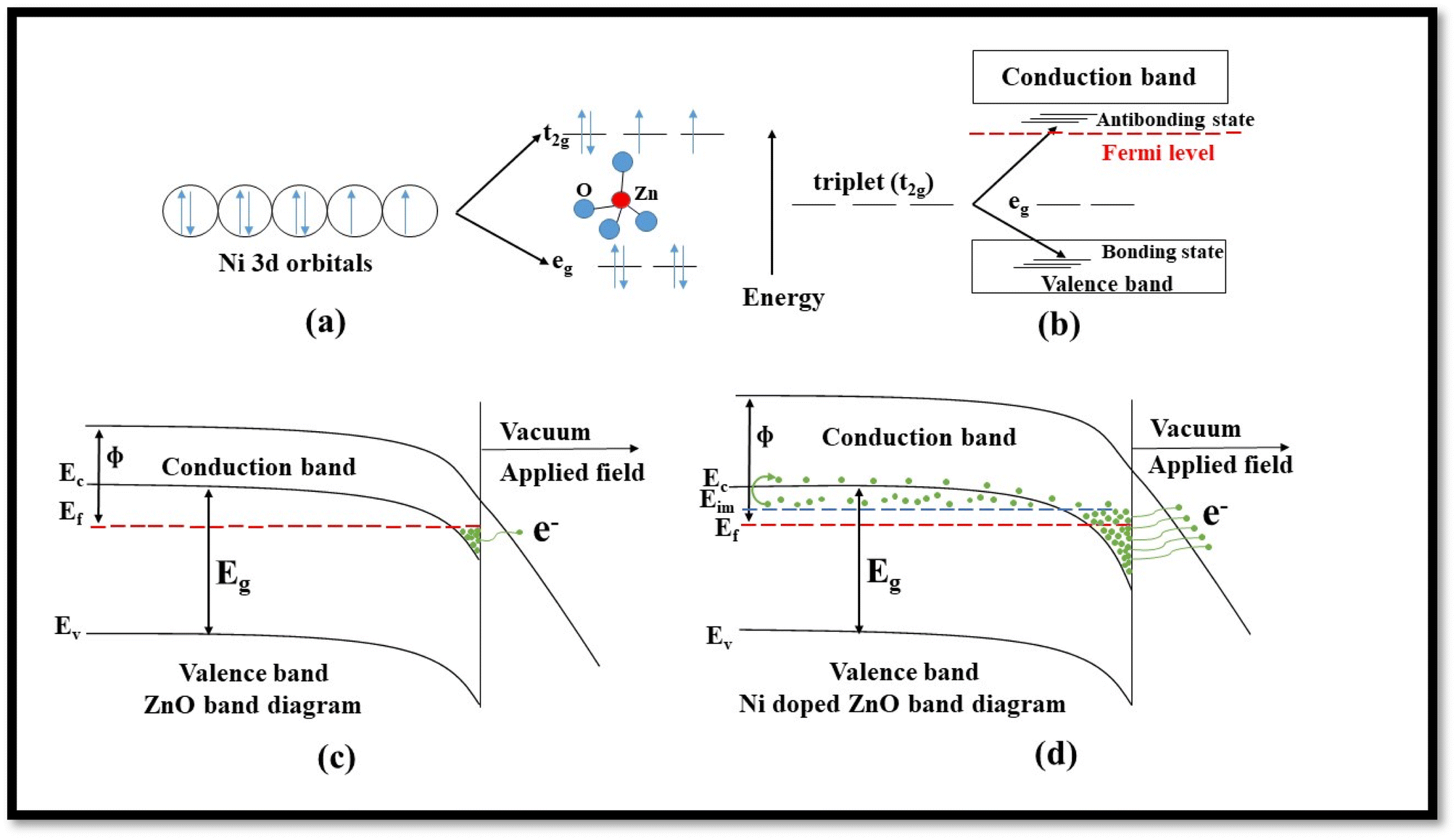 | ||
| Fig. 11 (a) Electronic structure of the transition metal at a substitution site in a wurtzite structure. (b) Splitting of the impurity state under the influence of a crystal field of host ZnO. Schematic energy band diagram of (c) ZnO and (d) Ni doped ZnO (Eg: energy gap, Ef: Fermi level, Ec: energy of the conduction band, Ev: energy of the valence band, and ϕ: work function). | ||
Doping of ZnO with transition metals like Ni results in a shift in energy levels and an enhanced carrier population in the conduction band of ZnO. In Ni-doped ZnO, Zn2+ ions, located in the middle of the tetrahedron surrounded by four oxygen atoms, get partially replaced by Ni2+ ions. As a result, the d orbital of Ni gets split into a higher triplet (t2g) and lower doublet (eg) state (Fig. 11a) under the crystal field of ZnO. After hybridization, the t2g state interacts with the p orbital of the valence electrons, causing it to split into bonding and anti-bonding t states (Fig. 11b). The t-bonding state is localized, while the t anti-bonding state has higher energy and is positioned very close to the conduction band. This anti-bonding state has a considerable number of mobile electrons, and there is a huge probability that a slight increase in the number of electrons from this impurity state can facilitate their transition into the conduction band of ZnO. This phenomenon leads to an enhancement in the field emission (FE) characteristics of sample B (Fig. 11c and d). Thus conclusively, it can be considered that due to the incorporation of Ni, a considerable number of electrons get promoted to the conduction band of ZnO and take part in the FE.
Similar results have been theoretically verified by many researchers from DFT studies.
For instance, Haq et al. computed the density of states of Ni-doped ZnO, which is shown in Fig. 12.59
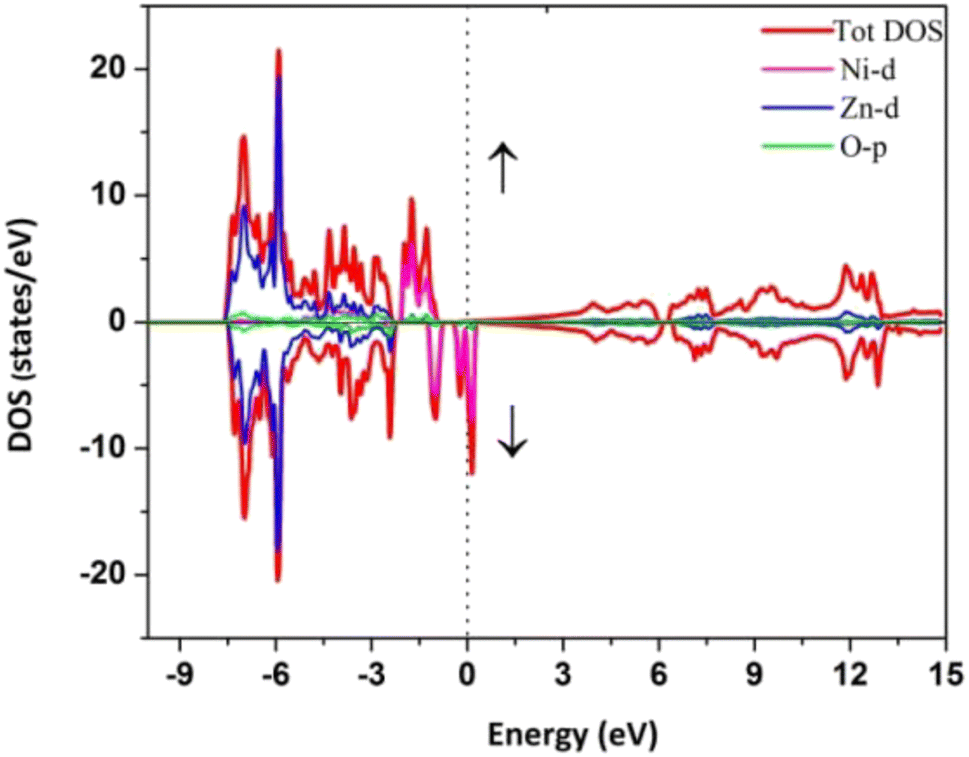 | ||
| Fig. 12 The spin polarized DOS of Ni doped ZnO. The spin up and down states are respectively plotted along +Y and −Y axes. The Fermi level is represented by the dotted line at 0 energy.59 | ||
Fig. 12 shows that the VB at a lower energy value is mostly contributed by the Zn-3d state, whereas the middle energy range contribution comes from Zn-3d, O-2p, and slightly from the Ni-3d level. The higher energy value of the VB (−2 to −1 eV) is solely due to Ni-3d together with the O-2p level. Due to the crystal field effect of oxygen, Ni 3d states are split into eg and t2g states, as mentioned before, and contributed to the FE characteristics of sample B.
Table 3 compares the cold emission result of different ZnO nanostructure-based systems to that of our present work.
| Sl no. | Sample | Synthesis method | E To at (V μm−1) | Electrode distance (μm) | Improvement [(ETo2 − ETo1)/ETo1] × 100 (%) | Ref. |
|---|---|---|---|---|---|---|
| 1 | Pd-adsorbed ZnO | Sputtering/wet chemical | 6.4–6.6 at 10 μA cm−2 | Not disclosed | 3.12 | 34 |
| 2 | In doped ZnO | Thermal oxidation | 7.1 10 μA cm−2 | Not disclosed | N/A | 35 |
| 3 | Ni doped ZnO nanowires and nano-tips | Thermal evaporation | 3.25 for nanowires | Not disclosed | 112 | 36 |
| 1.53 for nanotips at 100 μA cm−2 | ||||||
| 4 | Sn doped ZnO tetrapod | Thermal evaporation | 3.91–1.96 at 10 μA cm−2 | 500 | 99 | 60 |
| 5 | Ni doped ZnO | Wet chemical | 2.5–2.3 at 1 μA cm−2 | Not disclosed | 8 | 37 |
| 6 | ZnO NW | MOCVD | 4.1 at 10 μA cm−2 | Not disclosed | N/A | 61 |
| 7 | CNT-ZnO hybrid | Solid state heating | 9.7–2.6 at 10 μA cm−2 | Not disclosed | 273 | 62 |
| 8 | Ge doped ZnO NW | CVD | 4.1–3.5 at 10 μA cm−2 | 300 | 17 | 63 |
| 9 | Cu doped ZnO QD | Wet chemical | 5.89–5.04 10 μA cm−2 | 500 | 16.8 | 64 |
| 10 | Al doped ZnO NRAs/graphene | CVD/sputtering/wet chemical | 1.80 V mm−1 | 170 | N/A | 65 |
| Cu doped ZnO NRAs/graphene | 1.51 V mm−1 | |||||
| Not defined | ||||||
| 11 | Ni doped ZnO NR | Wet chemical | 2.84–5.34 1 μA cm−2 | 300 | 88 | Present work |
It is clearly seen that the present work gives results comparable to or sometimes even better than other reported results with the further advantage of a large inter-electrode distance and, most importantly, higher relative improvement of the hybrid system comparable to the pure one.
4. Conclusion
The present work concludes that it is possible to enhance the cold emission properties of ZnO nanorods by simply doping them with nickel, with atomic concentrations as low as 2%. Both pure and doped samples were synthesized by a simple wet chemical route and characterized by using various sophisticate tools. XRD confirms the proper phase formation, whereas XPS supports successful doping. XPS further suggests that the ZnO nanorod (confirmed by a FESEM study) contains significant oxygen vacancies in the case of the doped sample, which has a marked effect on PL as well as on the cold emission properties of the sample. A UV-vis study shows that the doped sample becomes significantly transparent after doping, with the band gap reduced from 2.97 to 2.12 eV. Not only that, as confirmed by a FTIR study, doping helps remove the hydroxyl group from pure ZnO, making it superhydrophobic.Cold emission current density undergoes an order enhancement after doping, reducing the turn-on field from 5.34 to 2.84 V μm−1, with an inter-electrode distance as high as 300 μm.
The enhancement factor for the doped sample is nearly 3500 and almost 1.5 times that of the pure sample.
The enhanced emission characteristics are believed to be due to the collective results of microstructures with a high aspect ratio, enhanced number of defect-induced states, favorable band bending, and carrier flow. Thus the present work successfully reports the synthesis of a ZnO-based superhydrophobic field emitter.
Conflicts of interest
There are no conflicts to declare.Acknowledgements
The authors wish to thank the Department of Science and Technology (DST, Gov't of India) for the financial support during the execution of the work (DST/TDT/DDP-52/2021). DB wants to thank Teerthanker Mahaveer University for providing financial support during the execution of this work under the seed money scheme (TMU/R.O/2020-21/Seed Money/028). PK, MP and KC want to thank Teerthanker Mahaveer University for granting them fellowship during the execution of the work.References
- D. B. Go, J. R. Haase, J. George, J. Mannhart, R. Wanke, A. Nojeh and R. Nemanich, Thermionic energy conversion in the twenty-first century: advances and opportunities for space and terrestrial applications, Front. Mech. Eng., 2017, 3, 13 CrossRef.
- M. Schwartz, New Materials, Processes, and Methods Technology, Crc Press, 2005 Search PubMed.
- K. Lange, Ultrafast Machining of High Temperature Superconducting Nanostructures for Novel Mesoscale Physics, Doctoral dissertation, University of Cambridge, 2021 Search PubMed.
- A. Patra, M. A. More, D. J. Late and C. S. Rout, Field emission applications of graphene-analogous two-dimensional materials: recent developments and future perspectives, J. Mater. Chem. C, 2021, 9(34), 11059–11078 RSC.
- M. Zhang and J. Li, Carbon nanotube in different shapes, Mater. Today, 2009, 12(6), 12–18 CrossRef CAS.
- A. K. Geim, Graphene: status and prospects, science, 2009, 324(5934), 1530–1534 CrossRef CAS PubMed.
- N. R. Dhineshbabu, V. Rajendran, N. Nithyavathy and R. Vetumperumal, Study of structural and optical properties of cupric oxide nanoparticles, Appl. Nanosci., 2016, 6, 933–939 CrossRef CAS.
- R. S. Kapadnis, S. B. Bansode, A. T. Supekar, P. K. Bhujbal, S. S. Kale, S. R. Jadkar and H. M. Pathan, Cadmium telluride/cadmium sulfide thin films solar cells: a review, ES Energy Environ., 2020, 10(2), 3–12 CAS.
- J. T. Richardson, D. I. Yiagas, B. Turk, K. Forster and M. V. Twigg, Origin of superparamagnetism in nickel oxide, J. Appl. Phys., 1991, 70(11), 6977–6982 CrossRef CAS.
- M. Batzill and U. Diebold, The surface and materials science of tin oxide, Prog. Surf. Sci., 2005, 79(2–4), 47–154 CrossRef CAS.
- D. G. Thomas, J. Phys. Chem. Solids, 1960, 15, 86 CrossRef CAS.
- Q. H. Li, Q. Wan, Y. J. Chen, T. H. Wang, H. B. Jia and D. P. Yu, Stable field emission from tetrapod-like ZnO nanostructures, Appl. Phys. Lett., 2004, 85(4), 636–638 CrossRef CAS.
- K. Takahashi, A. Yoshikawa and A. Sandhu, Wide Bandgap Semiconductors, Verlag Berlin Heidelberg, 2007 Search PubMed.
- O. Lupan, T. Pauporté, L. Chow, B. Viana, F. Pellé, L. K. Ono, B. R. Cuenya and H. Heinrich, Effects of annealing on properties of ZnO thin films prepared by electrochemical deposition in chloride medium, Appl. Surf. Sci., 2010, 256(6), 1895–1907 CrossRef CAS.
- H. Morkoç and Ü. Özgür, Zinc Oxide: Fundamentals, Materials and Device Technology, John Wiley & Sons, 2008 Search PubMed.
- M. V. Kovalenko, L. Manna, A. Cabot, Z. Hens, D. V. Talapin, C. R. Kagan, V. I. Klimov, A. L. Rogach, P. Reiss, D. J. Milliron and P. Guyot-Sionnnest, Prospects of nanoscience with nanocrystals, ACS Nano, 2015, 9(2), 1012–1057 CrossRef CAS PubMed.
- R. K. Joshi and J. J. Schneider, Assembly of one dimensional inorganic nanostructures into functional 2D and 3D architectures. Synthesis, arrangement and functionality, Chem. Soc. Rev., 2012, 41(15), 5285–5312 RSC.
- J. X. Wang, X. W. Sul, Y. Yang, H. Huang, Y. C. Lee, O. K. Tan and L. Vayssieres, Hydrothermally grown oriented ZnO nanorod arrays for gas sensing applications, Nanotechnology, 2006, 17, 4995–4998 CrossRef CAS.
- D. Klemm, E. D. Cranston, D. Fischer, M. Gama, S. A. Kedzior, D. Kralisch, F. Kramer, T. Kondo, T. Lindström, S. Nietzsche and K. Petzold-Welcke, Nanocellulose as a natural source for groundbreaking applications in materials science: Today's state, Mater. Today, 2018, 21(7), 720–748 CrossRef CAS.
- L. Schlur, A. Carton, P. Lévêque, D. Guillon and G. Pourroy, Optimization of a new ZnO nanorods hydrothermal synthesis method for solid state dye sensitized solar cells applications, J. Phys. Chem. C, 2013, 117, 2993–3001 CrossRef CAS.
- T. Sun, J. Qiu and C. Liang, Controllable fabrication and photocatalytic activity of ZnO nanobelt arrays, J. Phys. Chem. C, 2008, 112, 715–721 CrossRef CAS.
- R. Vladoiu, M. Tichý, A. Mandes, V. Dinca and P. Kudrna, Thermionic Vacuum Arc—A versatile technology for thin film deposition and its applications, Coatings, 2020, 10(3), 211 CrossRef CAS.
- Q. H. Li, Q. Wan, Y. J. Chen, T. H. Wang, H. B. Jia and D. P. Yu, Stable field emission from tetrapod-like ZnO nanostructures, Appl. Phys. Lett., 2004, 85(4), 636–638 CrossRef CAS.
- Z. Zhang, D. Chen, W. Chen, Y. Chen, X. Song, R. Zhan, S. Deng, N. Xu and J. Chen, Thermo-enhanced field emission from ZnO nanowires: Role of defects and application in a diode flat panel X-ray source, Appl. Surf. Sci., 2017, 399, 337–345 CrossRef CAS.
- Y. Lv, J. Liu, Z. Zhang, W. Zhang, A. Wang, F. Tian, W. Zhao and J. Yan, Hydrothermal synthesis of brush-like ZnO NWAs@ CC composites with enhanced photocatalytic and field emission performance, Mater. Sci. Semicond. Process., 2021, 135, 106043 CrossRef CAS.
- J. Singh and A. Srivastava, Morphological evolution and its correlation with optical and field emission properties in pulsed laser deposited ZnO nanostructures, Mater. Sci. Semicond. Process., 2022, 138, 106282 CrossRef CAS.
- Z. Ye, X. Ji and Q. Zhang, Enhanced field emission properties of ZnO nanorods by surface modification, RSC Adv., 2015, 5(96), 78502–78507 RSC.
- J. Ding, H. Chen, L. Ma, H. Fu and X. Wang, Field emission of graphene oxide decorated ZnO nanorods grown on Fe alloy substrates, J. Alloys Compd., 2017, 729, 538–544 CrossRef CAS.
- Y. Li, Z. Zhang, G. Zhang, L. Zhao, S. Deng, N. Xu and J. Chen, Optimizing the field emission properties of ZnO nanowire arrays by precisely tuning the population density and application in large-area gated field emitter arrays, ACS Appl. Mater. Interfaces, 2017, 9(4), 3911–3921 CrossRef CAS PubMed.
- S. J. Young, Y. H. Liu and J. T. Chien, Improving field electron emission properties of ZnO nanosheets with Ag nanoparticles adsorbed by photochemical method, ACS Omega, 2018, 3(7), 8135–8140 CrossRef CAS PubMed.
- P. J. Cao, Z. B. Yang, C. N. Rao, S. Han, W. Y. Xu, M. Fang, X. K. Liu, F. Jia, Y. X. Zeng, W. J. Liu and D. L. Zhu, Field emission properties of molybdenum nanoparticles decorated ZnO nanorod arrays, J. Nanosci. Nanotechnol., 2019, 19(12), 8135–8142 CrossRef CAS PubMed.
- A. Nagar, A. Kumar, S. Parveen, A. Kumar, H. Dhasmana, S. Husain, A. Verma and V. K. Jain, Zinc oxide nanoflowers synthesized by sol–gel technique for field emission displays (FEDs), Mater. Today: Proc., 2020, 32, 402–406 CAS.
- J. Liu, W. Zhang, A. Wang, Z. Zhang and Y. Lv, Preparation and Field Emission Performance of Metal-Doped ZnO NRAs/Graphene Composite Material, Integr. Ferroelectr., 2020, 209(1), 98–109 CrossRef CAS.
- S. J. Young and Y. L. Chu, Characteristics of field emitters on the basis of Pd-adsorbed ZnO nanostructures by photochemical method, ACS Appl. Nano Mater., 2021, 4(3), 2515–2521 CrossRef CAS.
- Y. Zhao, Y. Chen, G. Zhang, R. Zhan, J. She, S. Deng and J. Chen, High current field emission from large-area indium doped ZnO nanowire field emitter arrays for flat-panel X-ray source application, Nanomaterials, 2021, 11(1), 240 CrossRef CAS PubMed.
- Y. C. Chang, Ni-doped ZnO nanotower arrays with enhanced optical and field emission properties, RSC Adv., 2014, 4(99), 56241–56247 RSC.
- A. K. Rana, P. Bankar, Y. Kumar, M. A. More, D. J. Late and P. M. Shirage, Synthesis of Ni-doped ZnO nanostructures by low-temperature wet chemical method and their enhanced field emission properties, RSC Adv., 2016, 6(106), 104318–104324 RSC.
- D. Banerjee, A. K. Anand, S. Ghosh, N. S. Das, B. Das, U. K. Ghorai and K. K. Chattopadhyay, Zinc oxide rod-coated cotton fabric: a super-hydrophobic material for self-cleaning and oil/water separation, Chem. Pap., 2022, 76(8), 4679–4690 CrossRef CAS.
- M. Chen, X. Wang, Y. H. Yu, Z. L. Pei, X. D. Bai, C. Sun, R. F. Huang and L. S. Wen, X-ray photoelectron spectroscopy and auger electron spectroscopy studies of Al-doped ZnO films, Appl. Surf. Sci., 2000, 158(1–2), 134–140 CrossRef CAS.
- M. Zhong, Y. Li, M. Tariq, Y. Hu, W. Li, M. Zhu, H. Jin and Y. Li, Effect of oxygen vacancy induced by pulsed magnetic field on the room-temperature ferromagnetic Ni-doped ZnO synthesized by hydrothermal method, J. Alloys Compd., 2016, 675, 286–291 CrossRef CAS.
- M. S. Abdel-Wahab, A. Jilani, I. S. Yahia and A. A. Al-Ghamdi, Enhanced the photocatalytic activity of Ni-doped ZnO thin films: Morphological, optical and XPS analysis, Superlattices Microstruct., 2016, 94, 108–118 CrossRef CAS.
- S. Sarkar, D. Banerjee, U. K. Ghorai, N. S. Das and K. K. Chattopadhyay, Size dependent photoluminescence property of hydrothermally synthesized crystalline carbon quantum dots, J. Lumin., 2016, 178, 314–323 CrossRef CAS.
- D. Pahari, N. S. Das, B. Das, K. K. Chattopadhyay and D. Banerjee, Tailoring the optical and hydrophobic property of zinc oxide nanorod by coating with amorphous graphene, Phys. E, 2016, 83, 47–55 CrossRef CAS.
- S. Taghavi Fardood, A. Ramazani and S. Woo Joo, Sol-gel synthesis and characterization of zinc oxide nanoparticles using black tea extract, J. Appl. Chem. Res., 2017, 11(4), 8–17 Search PubMed.
- D. Liu, W. Wu, Y. Qiu, S. Yang, S. Xiao, Q. Q. Wang, L. Ding and J. Wang, Surface functionalization of ZnO nanotetrapods with photoactive and electroactive organic monolayers, Langmuir, 2008, 24(9), 5052–5059 CrossRef CAS PubMed.
- S. R. Senthilkumar and T. Sivakumar, Green tea (Camellia sinensis) mediated synthesis of zinc oxide (ZnO) nanoparticles and studies on their antimicrobial activities, Int. J. Pharm. Pharm. Sci., 2014, 6(6), 461–465 Search PubMed.
- S. Nandy, B. Saha, M. K. Mitra and K. K. Chattopadhyay, Effect of oxygen partial pressure on the electrical and optical properties of highly (200) oriented p-type Ni 1− x O films by DC sputtering, J. Mater. Sci., 2007, 42, 5766–5772 CrossRef CAS.
- T. N. Ravishankar, K. Manjunatha, T. Ramakrishnappa, G. Nagaraju, D. Kumar, S. Sarakar, B. S. Anandakumar, G. T. Chandrappa, V. Reddy and J. Dupont, Comparison of the photocatalytic degradation of trypan blue by undoped and silver-doped zinc oxide nanoparticles, Mater. Sci. Semicond. Process., 2014, 26, 7–17 CrossRef CAS.
- A. Grill and D. A. Neumayer, Structure of low dielectric constant to extreme low dielectric constant SiCOH films: Fourier transform infrared spectroscopy characterization, J. Appl. Phys., 2003, 94(10), 6697–6707 CrossRef CAS.
- S. Pirsa, T. Shamusi and E. M. Kia, Smart films based on bacterial cellulose nanofibers modified by conductive polypyrrole and zinc oxide nanoparticles, J. Appl. Polym. Sci., 2018, 135(34), 46617 CrossRef.
- R. A. Masud, M. S. Islam, P. Haque, M. N. I. Khan, M. Shahruzzaman, M. Khan, M. Takafuji and M. M. Rahman, Preparation of novel chitosan/poly (ethylene glycol)/ZnO bionanocomposite for wound healing application: effect of gentamicin loading, Materialia, 2020, 12, 100785 CrossRef CAS.
- A. A. Barzinjy, S. M. Hamad, M. M. Esmaeel, S. K. Aydın and F. H. S. Hussain, Biosynthesis and characterisation of zinc oxide nanoparticles from Punica granatum (pomegranate) juice extract and its application in thin films preparation by spin-coating method, Micro Nano Lett., 2020, 15(6), 415–420 CrossRef CAS.
- J. Wang, Y. Li, Y. Kong, J. Zhou, J. Wu, X. Wu, W. Qin, Z. Jiao and L. Jiang, Non-fluorinated superhydrophobic and micro/nano hierarchical Al doped ZnO film: the effect of Al doping on morphological and hydrophobic properties, RSC Adv., 2015, 5(99), 81024–81029 RSC.
- D. Banerjee, S. Mukherjee and K. K. Chattopadhyay, Controlling the surface topology and hence the hydrophobicity of amorphous carbon thin films, Carbon, 2010, 48(4), 1025–1031 CrossRef CAS.
- D. Kundu, D. Banerjee, S. Ghosh, R. C. Tewari, N. S. Das, B. Das and K. K. Chattopadhyay, Achievement of nearly super hydrophobicity in plasma enhanced chemical vapour deposited one and two dimensional carbon nanostructures, Phys. E, 2019, 108, 7–14 CrossRef CAS.
- R. H. Fowler and L. Nordheim, Electron emission in intense electric fields, Proc. R. Soc. London, Ser. A, 1928, 119(781), 173–181 CAS.
- C. Chai, H. Liu and W. Yu, The electronic and optical properties of the Fe, Co, Ni and Cu doped ZnO monolayer photocatalyst, Chem. Phys. Lett., 2021, 778, 138765 CrossRef CAS.
- S. Chen, J. Chen, J. Liu, J. Qi and Y. Wang, The effect of high-temperature oxygen annealing on field emission from ZnO nanowire arrays, Appl. Surf. Sci., 2015, 357, 413–416 CrossRef CAS.
- B. U. Haq, R. Ahmed, A. Afaq, A. Shaari and M. Zarshenas, Structural and electronic properties of ni-doped ZnO in zinc-blende phase: A DFT investigations, AIP Conf. Proc., 2012, 1482(1), 54–57 CrossRef.
- X. Zhou, T. Lin, Y. Liu, C. Wu, X. Zeng, D. Jiang, Y. A. Zhang and T. Guo, Structural, optical, and improved field-emission properties of tetrapod-shaped Sn-doped ZnO nanostructures synthesized via thermal evaporation, ACS Appl. Mater. Interfaces, 2013, 5(20), 10067–10073 CrossRef CAS PubMed.
- S. Haugg, C. Hedrich, R. Zierold and R. H. Blick, Field emission characteristics of ZnO nanowires grown by catalyst-assisted MOCVD on free-standing inorganic nanomembranes, J. Phys. D: Appl. Phys., 2022, 55(25), 255104 CrossRef.
- S. Maity and K. K. Chattopadhyay, Enhanced Cold Cathode Electron Emission from ZnO Nanostructure Attached Amorphous Carbon Nanotubes, in The Physics of Semiconductor Devices: Proceedings of IWPSD 2017, Springer International Publishing, 2019, pp. 1195–1201 Search PubMed.
- Y. Liang, Ge-doped ZnO nanowire arrays as cold field emitters with excellent performance, Nanotechnology, 2019, 30(37), 375603 CrossRef CAS PubMed.
- L. Sun, Z. Lin, X. Zhou, Y. Zhang and T. Guo, Synthesis of Cu-doped ZnO quantum dots and their applications in field emission, J. Alloys Compd., 2016, 671, 473–478 CrossRef CAS.
- J. Liu, W. Zhang, A. Wang, Z. Zhang and Y. Lv, Preparation and Field Emission Performance of Metal-Doped ZnO NRAs/Graphene Composite Material, Integr. Ferroelectr., 2020, 209(1), 98–109 CrossRef CAS.
| This journal is © The Royal Society of Chemistry 2023 |