
 Open Access Article
 This Open Access Article is licensed under a Creative Commons Attribution-Non Commercial 3.0 Unported Licence
Physical probing of quantum energy levels in a single indium arsenide (InAs) quantum dot
Moh'd
Rezeq
*ab,
Yawar
Abbas
 ab,
Boyu
Wen
c,
Zbig
Wasilewski
c and
Dayan
Ban
*c
ab,
Boyu
Wen
c,
Zbig
Wasilewski
c and
Dayan
Ban
*c
aDepartment of Physics, Khalifa University of Science and Technology, POB 127788, Abu Dhabi, United Arab Emirates. E-mail: mohd.rezeq@ku.ac.ae
bSystem on Chip Centre, Khalifa University of Science and Technology, POB 127788, Abu Dhabi, United Arab Emirates
cDepartment of Electrical and Computer Engineering, Waterloo Institute for Nanotechnology, University of Waterloo, ON, Canada. E-mail: dban@uwaterloo.ca
First published on 18th September 2023
Abstract
Indium arsenide (InAs) quantum dots (QDs) grown by molecular beam epitaxy (EBM) on gallium arsenide (GaAs) substrates have exhibited quantized charge-trapping characteristics. An electric charge can be injected in a single QD by a gold-coated AFM nano-probe placed directly on it using a conductive-mode atomic force microscope (C-AFM). The results revealed separate current–voltage (I–V) curves during consecutive measurements, where the turn-on voltages measured at the subsequent voltage sweeps are incrementally lower than that at the initial sweep. We demonstrate that the charge state of the QD can change over a long enough time by measuring the I–V data on the same QD at different time intervals. Discrete energy states (here, five states) have been observed due to the quantized charge leakage from the QD into the surrounding materials. These quantum states with five energy levels have been verified using quantum theory analysis of the quantum-well with the help of a numerical simulation model, which depends on the QD dimensions. The size of the quantum-well in the model is in good agreement with the actual QD size, whose lateral dimension is confirmed using a scanning electron microscope. At the same time, the height is estimated from the atomic force microscope topography.
1. Introduction
There is a growing interest in developing technologies for devices with extremely small dimensions, for less energy consumption and higher switching speed.1–3 Nano-scale semiconductor-based devices attracted lots of attention due to their unconventional electrical and optical properties.4–6 Several approaches and materials are being intensively investigated to develop small-scale devices, like carbon nanotubes, nanowires, nanoparticles, and graphene-based devices.7–11 Understanding the electronic structure at the nanoscale is crucial for applications in nano-electronic device design and fabrication, where the electrical characteristics are significantly dominated by the size of metal–semiconductor interfaces.12–15Quantum dots have emerged as a viable technique for semiconductor devices, notably in memory technology.16,17 To mention some of the significant benefits, the size and shape of quantum dots at nano-scale semiconductor crystals can be precisely controlled.18,19 This enables exact adjustment of their electrical characteristics, such as energy levels and bandgaps. The homogeneity of quantum dots makes it possible to design memory systems that are quite reliable and repeatable.20,21 The customizable characteristics of quantum dots are another benefit. Since quantum dots have size-dependent optoelectronic characteristics, their behavior can be modified by varying their size.22,23 The number of energy states directly depends on the dimensions of the quantum dot, increasing the dimensions of the QD increases the number of quantum states, hence, the number of energy levels. Moreover, changing the material of the quantum dot will change the number of quantum states in the quantum well, which is inversely proportional to the band gap of the quantum dot. With this tunability, memory devices can be created with the appropriate properties, including certain energy levels, emission wavelengths, and charge-storage capacities. Furthermore, their sturdy construction reduces surface-related flaws and deterioration, allowing for sustained device operation and data storage in memory technology. Therefore, quantum dots offer unmatched benefits over other nanomaterials like nanowires, and nanosheets for developing high-performance and reliable memory devices, because of the above-mentioned characteristics, and improved stability. Due to the extremely small size of the quantum dots, where each QD is a nanoscale unit memory cell with multilevel energy states, they offer a potential memory platform with a memory density higher than traditional CMOS technology. Additionally, they provide a low power consumption platform capable of retaining the data without refreshing. Therefore, the fast data access, low power consumption, and high-density memory of QDs have the potential to revolutionize the semiconductor memory technology.16,24
Here we investigate InAs QDs grown on a GaAs substrate for promising applications in nano-devices, like memory devices. The electrical characteristics of individual nanoparticles (NPs) and QDs can be measured by placing a metal-coated probe directly on them, using conductive-mode atomic force microscopy (C-AFM), where the current–voltage curves on individual NPs or QDs can be measured.25–27 Upon sweeping the voltage on the sample between negative and positive values, we discovered that some charges, or electrons, get trapped in the QD. This results in a shift in the I–V curves.27
Herein, we demonstrate that after waiting for some time intervals and repeating these I–V measurements, discrete I–V curves can be obtained with different turn-on (threshold) voltages, which can be attributed to the charge leakage from the QD into the surrounding material. This happens because these trapped electrons occupy specific energy levels in the QD, which results in different Fermi-level pinning states at the surface, and hence different forward bias turn-on voltages. The I–V results indicate direct probing of the energy states of the electrons in that particular QD. The size of the QD has been verified using the atomic force microscope (AFM) topography and the field emission scanning electron microscope (FESEM) images. Numerical simulation has been performed based on the quantum theory of electrons confined in a quantum-well. The results agreed with the energy level states observed experimentally for a QD with a size similar to that observed in the SEM and AFM. We would like to indicate here that unlike other work,28,29 where a large number of QDs are used collectively for charge storage and detection in a relatively large-scale space-charge region, here an individual QD is measured at a time using a conductive nano-probe. This allows us to study the energy states of electrons trapped in a single QD.
2. Experimental procedure, results and discussion
Low-density distribution of well-separated indium arsenide (InAs) quantum dots (QDs) were grown by using the molecular beam epitaxy (MBE) technique. A thin layer of 2.4 Å of InAs was deposited on the GaAs surface. This amount has reached 2D–3D transition after approximately 30 seconds of annealing time under As flux, as observed with RHEED. The growth mechanism of the substrate and the QDs on the surface was detailed in a previous work.27 To protect the surface of the QDs from oxidization, a thin amorphous Arsenic (As) cap was deposited on the top of the structure. A conductive mode atomic force microscope (C-AFM) was used to obtain a topographical image of the surface of the sample. During the AFM topography, we used a scan rate of 0.5 Hz, and the resonance frequency of the tip used for scanning was 270 kHz. Then the C-AFM was used to perform the electrical characterization on an individual QD using a conductive gold-coated nano-probe. The AFM probe was characterized in a scanning electron microscope (SEM) before scanning and I–V measurements, where a well-defined gold-coated AFM probe was selected and used in the measurements.The MBE-grown InAs-QDs were analyzed using a C-AFM and SEM, as shown in Fig. 1. Fig. 1(a) shows the schematic diagram of the electrical measurement setup carried out on an individual QD. In ASYLUM MFP3D AFM, the conducting tip is always at the ground and a voltage bias is applied on the sample. For better electrical contact, the back of the substrate is scratched and attached with the gold-coated disc using a conductive silver paint.
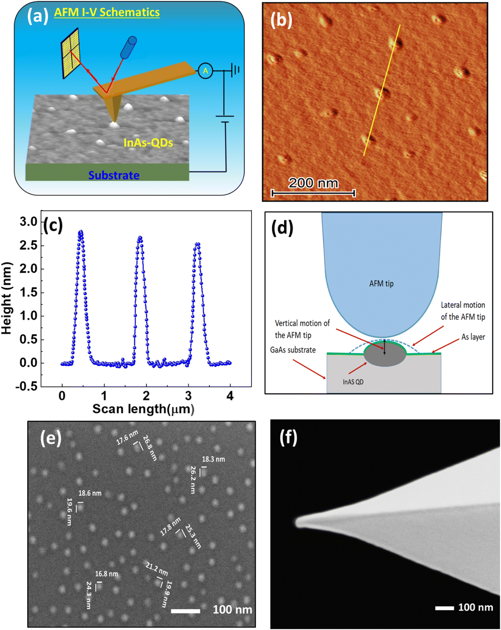 | ||
| Fig. 1 (a) The schematic of the C-AFM setup. (b) The AFM topographic image of InAs QDs on the sample surface. (c) The height profile of QDs along the line drawn along QDs in (b). (d) A schematic shows the effect of the tip apex diameter on the lateral dimensions of the QD. (e) A FESEM image of QDs. (f) A FESEM image of the nanoprobe used in this experiment. | ||
Fig. 1(b) depicts the atomic force microscope (AFM) topography image of QDs, which are well separated and distributed on the surface. The height profile along the line shown in Fig. 1(b) and plotted in Fig. 1(c) indicates that the QDs' height is around 2.5–3.0 nm, with lateral dimensions in the range of 35–50 nm. It is well known in AFM topographical imaging process that the AFM tip size rather dominates the lateral resolution. In contrast, the vertical resolution depends directly on the object's height, which is controlled by the AFM piezoelectric vertical motion, as illustrated in the schematic in Fig. 1(d). Therefore, the height of the QD can be estimated to reasonable proximity from the profile in Fig. 1(c).
Therefore, the lateral size imaged in AFM is a combination of the actual dot topography and the AFM probe radius. In fact, the lateral scale of the QD is rather dependent on the AFM probe apex size, as demonstrated in Fig. 1(d). However, to confirm the lateral dimensions of the QDs, we analyzed the sample in SEM. The SEM image in Fig. 1(e) depicts that these QDs are not perfectly circular but nearly elliptical in shape with dimensions between 16 nm to 27 nm, as indicated by perpendicular scale bars around selected QDs. Some QDs showed scale bars of around 18 nm × 26 nm, which is very close to what was predicted theoretically.15 Furthermore, it is observed that the distance between QDs ranges from 70 to 200 nm, which means that there will be no crosstalk between two nearby QDs, i.e., the electrical probing on one QD will not affect the quantum states in its adjacent QDs. Fig. 1(f) shows the SEM micrograph of the gold-coated nano-probe with a diameter of ∼25 nm. These InAs QDs are conventional and self-assembled, and have a lens-shape,30 which can be inferred by comparing the lateral dimension with the vertical height from the profile in Fig. 1(c) and (d).
Fig. 2(a–d) shows the electrical measurement results on an individual QD. After getting a clear topographic image in a scan area of 600 nm × 600 nm, some QDs are randomly selected on the surface of the sample, as shown in the insets of Fig. 2(a), (b) and (d), to carry out the electrical measurements, The Au probe of AFM is then placed directly in a physical contact with a pre-selected QD, as shown in the schematic in Fig. 1(a). Before the measurements, the AFM tip was connected to the ground and a voltage bias was applied on the GaAs substrate. Subsequently, the electrical current through the AFM probe/QD junction was measured by sweeping the voltage bias from −3.0 V to +3.0 V.
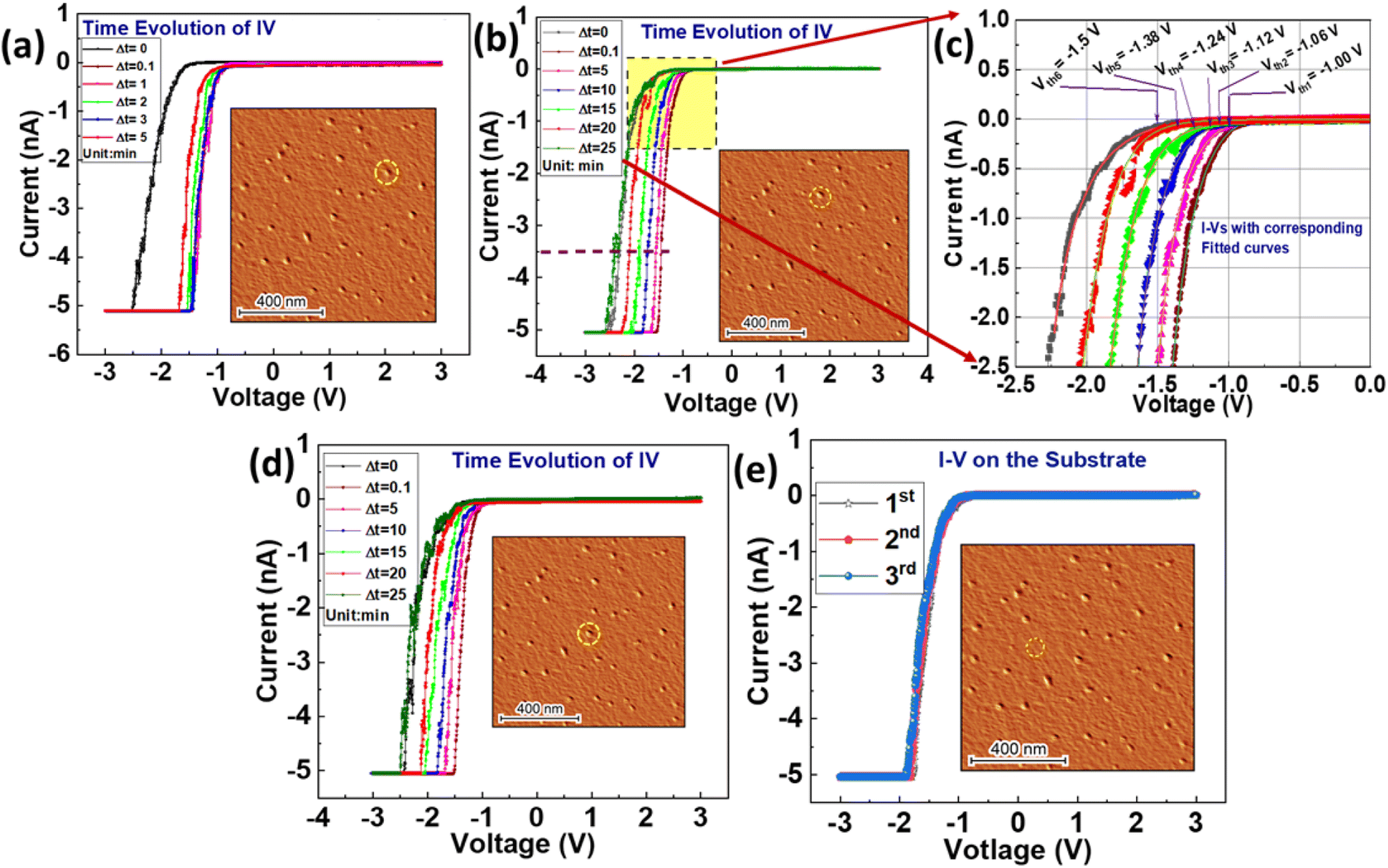 | ||
| Fig. 2 (a) The time evolution of the quantum state after short time intervals. (b) The time evolution of the electrical characteristics at the location of QD shows shifting in the turn-on voltages. (c) The magnified and exponentially fitted I–V curves from the highlighted region in Fig. 1(b). (d) The electrical characteristics on the surface of another predefined QD. (e) The electrical characteristics directly on the surface of GaAs substrate without a QD. | ||
A series of I–V measurements were performed on individual QDs as shown in Fig. 2(a), (b) and (d). A typical Schottky junction characteristics was observed,8,31 where under a reverse bias the measured current is minimum. Under a forward bias (negative applied voltage), the measured current is turned on at a voltage around ∼−1.5 V, and increases rapidly until it reaches the AFM amplifier saturation value of 5.0 nA at an applied voltage around −2.5 V. From the experimental data, the initial measured I–V curve (the 1st time voltage sweep) has a higher turn-on voltage compared with the successive immediate scans. The latter has a lower turn-on voltage (∼−1.0 V), compared to the first one at (∼−1.5 V), and reaches the saturation current at a much lower voltage (∼−1.5 V), compared to that at the 1st scan at (∼−2.5 V), as shown in Fig. 2(a), (b) and (d). For the validation of these results, the I–V measurements were repeated on more than 20 QDs, and a similar electrical behavior was observed.
We have observed that repeating the I–V measurements immediately and within time intervals of less than ∼4 minutes from the previous one, as the QD will be charged again during each I–V sweep, always results in overlapping I–V curves, as shown in Fig. 2(a). However, by increasing the wait time to ∼5 minutes, the I–V curve in the forward bias, opens up and takes a new path with a slightly higher turn-on voltage. This indicates a lower potential at the QD due to charge leakage. Repeating these measurements after additional five minutes results in a new I–V curve with a clear shift from the previous one, in the forward bias as shown in Fig. 2(b). After 5 measurements, each time we wait additional 5 minutes, i.e. in the last measurement the wait-time was 25 minutes from the previous one, the I–V curve overlap with the initial curve we started with. This indicate a completely discharged QD. To calculate the time evolution of turn-on or threshold voltages (Vth) of each I–V sweep, the I–V curves in the highlighted region of Fig. 2(b) are replotted in Fig. 2(c) after they are fitted with the exponential curves. The calculated threshold voltages are, −1.00 V, −1.06 V, −1.12 V, −1.24 V, −1.38 V, and −1.50 V. For further confirmation, the same measurements were repeated with similar conditions, and the same results observed, as in Fig. 2(d). After waiting for more than 25 minutes, the quantum dot will stay in its empty state, thus any later I–V measurement will be the same as that for the initial state. We would like to indicate that the charge trapping effect is not evident when the probe is placed on GaAs surface in the absence of the QD, as shown here in Fig. 2(e), and demonstrated in a previous work ref. 2.
For further investigation on the energy levels at the QD, in a new experiment, we have applied voltage pulses at a selected current value chosen from Fig. 2(b), which corresponds to a current of 3.5 nA along the horizontal dashed line. This current corresponds to forward (negative) voltage biases −2.30 V, −1.50 V, −1.60 V, −1.70 V, −1.90 V, −2.10 V, and −2.30 V. We have applied these voltage pulses after waiting times 0, 5, 10, 15, 20, 25 minutes. The duration of each pulse is one second. The measured current is quite similar to the selected current from the I–V curves in Fig. 2(b), which can be clearly shown in Fig. 3. This demonstrates that a set current can be read at a given voltage pulse, which would have potential applications for memory devices.
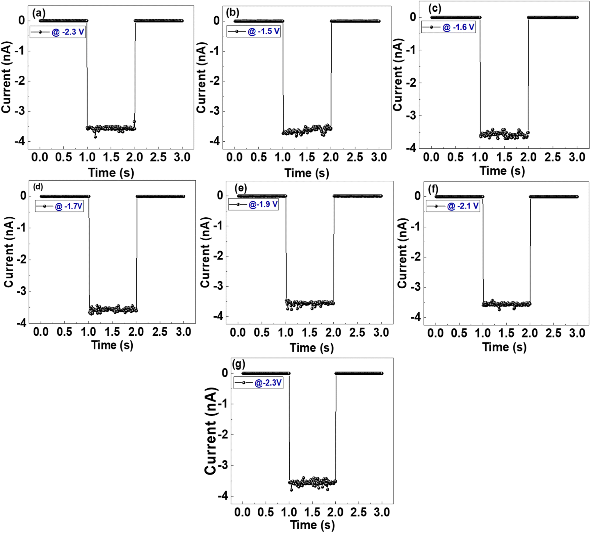 | ||
| Fig. 3 (a)–(g) Investigation of energy levels in QDs at a set input voltage pulses, 2.3, 1.5,1.6, 1.7, 1.9, 2.1 and 2.3 V respectively, while a similar reading current (3.5 nA) is observed. | ||
3. Data analysis and simulation
The shift in the “turn-on” or “threshold” voltages between the initial and the consecutive voltage sweeps is attributed to the Fermi level pinning at different energy states of the QD, i.e. due to the trapping of electrons in different quantum energy levels. However, after waiting for a long enough time, some charges, i.e. electrons, leak out into the surrounding material. This results in lowering the QD's energy level, hence lowering the Fermi level pinning in the bulk. Consequently, a higher turn-on voltage will be required again to overcome the forward bias barrier height. Fig. 4 schematically shows the energy band diagram for a QD between the AFM Au-tip, the thin As layer, the InAs-QD and the GaAs substrate (Al-doped and undoped lattices). Fig. 4(a) shows the energy band diagram when the QD is empty and before applying any voltage sweeps. The conduction band of GaAs is bent down until the Fermi level alignment is achieved across the stack of all materials. Then at a forward (negative) and a turn-on (a threshold) voltage V1-on is required to lift up the energy level of the conduction band to allow electrons to drift over the conduction band to the QD and subsequently to the tip, over As thin layer barrier edge. During this process, some electrons get trapped inside the quantum well. The trapped electrons will accumulate in the potential-well between GaAs and As layer until they reach to a level similar to the bulk conduction band but lower than the barrier edge of As layer. The GaAs bulk conduction band is bent down and Fermi level is now pinned at the new electronic state of the QD, which is shifted up by an amount ΔV, as shown in the schematic in Fig. 4(b). Consequently, a less turn-on voltage (V2-on) is required at the consecutive voltage sweeps to drive electrons over the forward bias barrier, as depicted in Fig. 4(b). Hence, the new turn-on voltage V2-on, equals V2-on = V1-on − ΔV.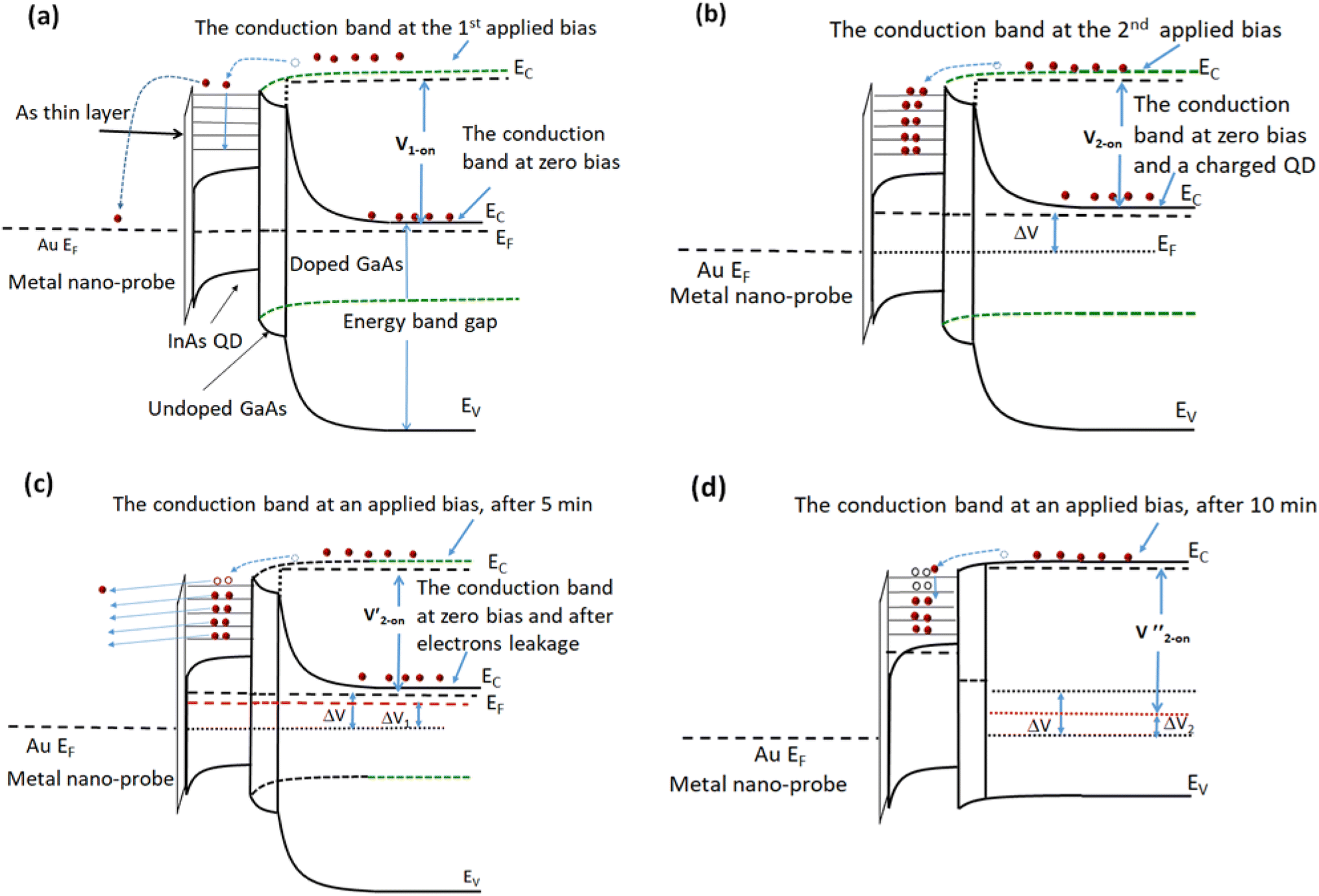 | ||
Fig. 4 Schematics of the energy band diagram for a QD located between the nano-probe and a GaAs bulk. (a) Show the energy band diagram and band-pending at the contact interface, before applying a bias voltage and after applying a threshold (turn-on) forward bias voltage, V1-on. (b) When the QD is fully charged the bottom of the conduction band is shifted up by ΔV, and the new trun-on voltage is V2-on = V1-on − ΔV. (c) After the leakage of electrons from the top energy level, after 5 minutes, the conduction band drop to ΔV1 < ΔV, which results in a higher turn-on voltage,  . (d) The energy band diagram at a forward bias and after the QD is discharged with two more electrons, . (d) The energy band diagram at a forward bias and after the QD is discharged with two more electrons, 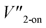 is higher than is higher than 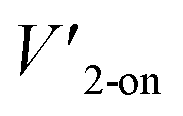 by 0.06 V. by 0.06 V. | ||
However, after a waiting time of ∼5 minutes some electrons leak out from one of the quantum states, in the QD (or the potential well), which results in a lower potential of the QD. From the I–V data in Fig. 2 and pulse data in Fig. 3, at a current value of 3.5 nA, we can readily infer that there is a discrete potential shift of 0.06 to 0.14 V, depending on the energy states, after a waiting time of additional 5 minutes from previous measurements. This means that each time the QDs potential energy drops by 0.06 to 0.14 eV, which affects the level of the bulk Fermi pinning. We have observed 5 discrete quantum states in addition to the empty state in the QD. Each energy level can occupy two electrons, with spin up and spin down, and hence 10 electrons can be trapped in the QD. This change in the turn-on (threshold) voltage is equivalent to the leakage of two electrons at a time, from each energy level, from the top to lower levels, as shown in the schematic in Fig. 4(c) and (d), and in the simulation model in Fig. 5. Fig. 4(c) shows the energy band diagram after the leakage of two electrons, where the Fermi level shift from that of the first sweep is ΔV1. A forward bias  is now higher than V2-on by a value equal to ΔV − ΔV1 ≅ 0.06 V. This sequence shift takes place in steps of 0.06 to 0.14 V, depending on the energy state, as in Fig. 4(d), where the turn-on voltage is
  , with a new shift in Fermi level ΔV2. This drop in Fermi level will continue until the QD is fully discharged and comes back to the initial stage as in Fig. 4(a).
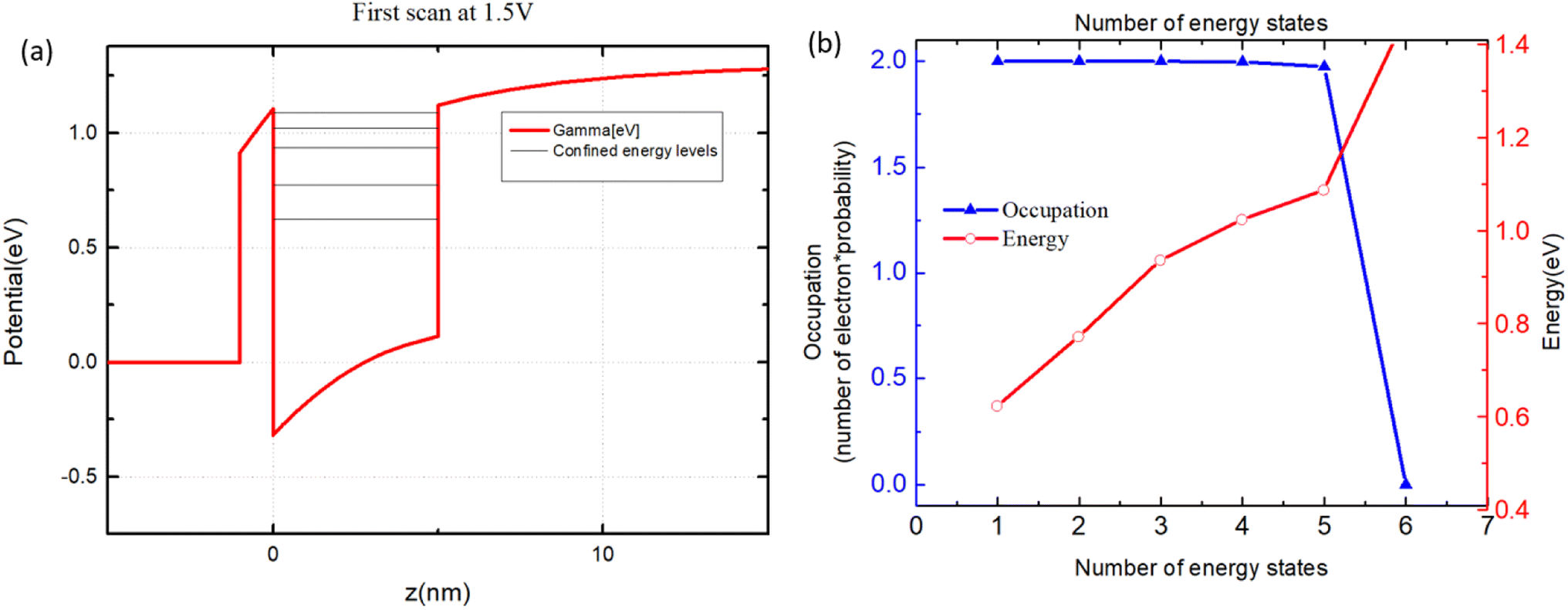 | ||
| Fig. 5 During the first scan, bias at 1.5 V. (a) Shows five energy states within the quantum-well. (b) The occupation possibility and energy of each energy state. | ||
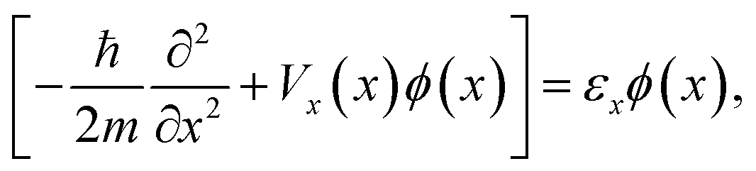
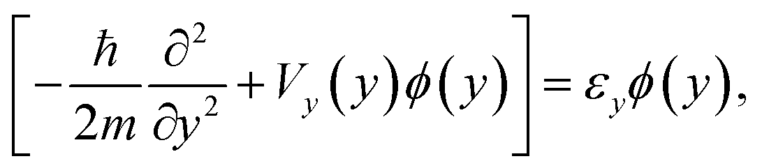
We have also performed finite element simulation analysis for calculating the energy states in a QD considering the band diagram at a bias voltage of 1.5 V with electrons trapped inside a QD in 3D, with dimensions 5 nm × 18 nm × 26 nm. The Poisson equation is solved in z-direction as described by
| ∇·[ε(z)∇ϕ(z)] = −ρ(z), | (1) |
 | (2a) |
 | (2b) |
 | (2c) |
| E = εx + εy + εz. | (3) |
The conduction band edge of the As thin layer at gamma point is ∼1.94 eV.27 The band gap and valence band offset of InAs/GaAs is around 0.417/1.519 eV and 1.39/1.346 eV, respectively.15 The doping level in GaAs substrate is estimated to be 1018 cm−3 with 15 nm undoped GaAs substrate on the top and in contact with the QD. Fig. 5(a) shows the conduction band profile of the system at 1.5 V bias at the first scan (without electrons trapped inside the QD before the scanning). Five energy states are present inside the QD when GaAs substrate edge is lifted above As layer's energy barrier by the applied bias of ∼1.5 V. Current starts increasing above this point, and energy states are filled. As time goes by after the first scan, electrons trapped inside QD leak out from state to state, from higher to lower. Therefore, the 6 discrete threshold voltages are measured in Fig. 2(c) corresponding to 0, 1, 2, 3, 4, 5 filled energy states, including the empty state. As shown in Fig. 5(b), the energy states occupation possibility of each energy state is calculated by solving the equation,
 | (4) |
4. Conclusion
A conductive nano-probe has been used to investigate the local electrical characteristics of individual QD in an atomic force microscope (AFM). After imaging QDs, the nano-probes is placed directly on a selected QD and the (I–V) measurements where performed. Discrete I–V curves were obtained immediately after sweeping the applied voltage and waiting 5 minutes between consecutive sweeps. This change in I–V behavior is attributed to the charge trap during the initial voltage sweep and to the charge leakage after waiting for some time. The discrete behavior in the I–V characteristic indicates discrete energy levels of trapped electrons inside the quantum well of the QD. Five quantum energy states have been found in a QD with dimensions of 5 nm × 18 nm × 26 nm, in addition to the empty state. These quantum states have also been verified using a numerical simulation model and calculations of the quantum state of a QD of similar dimensions. These results provide a physical approach for detecting the quantum states in a single QD, which would utilize such QDs in multi-level based data-storage nano-devices.Author contributions
Moh'd Rezeq: physical concepts and models, methodology, data analysis, and paper drafting. Yawar Abbas: investigations and measurements. Boyu Wen: data simulation and analysis. Zbig Wasilewski: material growth and analysis. Dayan Ban: conceptualization, simulation, and data analysis. All authors reviewed the paper.Conflicts of interest
There is no conflict of interest to declare.Acknowledgements
The experimental measurements have been performed using the characterization lab facility at Khalifa University.References
- T. N. Theis and H.-S. P. Wong, Comput. Sci. Eng., 2017, 19, 41–50 Search PubMed.
- J. S. Meena, S. M. Sze, U. Chand and T.-Y. Tseng, Nanoscale Res. Lett., 2014, 9, 1–33 CrossRef PubMed.
- S. Chen, M. R. Mahmoodi, Y. Shi, C. Mahata, B. Yuan, X. Liang, C. Wen, F. Hui, D. Akinwande and D. B. Strukov, Nat. Electron., 2020, 3, 638–645 CrossRef CAS.
- M. de Cea, A. Atabaki and R. Ram, Nat. Commun., 2021, 12, 2326 CrossRef CAS PubMed.
- C. Deepa, L. Rajeshkumar and M. Ramesh, J. Mater. Res. Technol., 2022, 12, 2657–2694 CrossRef.
- S. Wei, Z. Li, A. John, B. I. Karawdeniya, Z. Li, F. Zhang, K. Vora, H. H. Tan, C. Jagadish and K. Murugappan, Adv. Funct. Mater., 2022, 32, 2107596 CrossRef CAS.
- W. Feng, W. Luo and Y. Feng, Nanoscale, 2012, 4, 6118–6134 RSC.
- Y. Abbas, A. Rezk, S. Anwer, I. Saadat, A. Nayfeh and M. Rezeq, Nanotechnology, 2020, 31, 125708 CrossRef CAS PubMed.
- Y. Abbas, M. U. Khan, F. Ravaux, B. Mohammad and M. Rezeq, ACS Appl. Nano Mater., 2022, 5, 18537–18544 CrossRef CAS.
- A. Rezk, Y. Abbas, I. Saadat, A. Nayfeh and M. Rezeq, Appl. Phys. Lett., 2020, 116, 223501 CrossRef CAS.
- M. Rezeq, C. Joachim and N. Chandrasekhar, Surf. Sci., 2009, 603, 697–702 CrossRef CAS.
- Y. Abbas, M. Rezeq, A. Nayfeh and I. Saadat, Appl. Phys. Lett., 2021, 119, 162103 CrossRef CAS.
- C.-W. Nan, A. Tschöpe, S. Holten, H. Kliem and R. Birringer, J. Appl. Phys., 1999, 85, 7735–7740 CrossRef CAS.
- S. A. Makhlouf, M. A. Kassem and M. Abdel-Rahim, J. Mater. Sci., 2009, 44, 3438–3444 CrossRef CAS.
- L. D. Geoffrion and G. Guisbiers, J. Phys. Chem. Solids, 2020, 140, 109320 CrossRef CAS.
- Z. Lv, Y. Wang, J. Chen, J. Wang, Y. Zhou and S.-T. Han, Chem. Rev., 2020, 120, 3941–4006 CrossRef CAS PubMed.
- A. Mubarakali, J. Ramakrishnan, D. Mavaluru, A. Elsir, O. Elsier and K. Wakil, Nano Commun. Netw., 2019, 21, 100252 CrossRef.
- H. Moon, C. Lee, W. Lee, J. Kim and H. Chae, Adv. Mater., 2019, 31, 1804294 CrossRef PubMed.
- Z. Wasilewski, S. Fafard and J. McCaffrey, J. Cryst. Growth, 1999, 201, 1131–1135 CrossRef.
- H. Lan and Y. Ding, Nano Today, 2012, 7, 94–123 CrossRef CAS.
- M. M. Rehman, G. U. Siddiqui, S. Kim and K. H. Choi, J. Phys. D: Appl. Phys., 2017, 50, 335104 CrossRef.
- A. Roberge, J. H. Dunlap, F. Ahmed and A. B. Greytak, Chem. Mater., 2020, 32, 6588–6594 CrossRef CAS.
- E. K. Vishnu, A. A. Kumar Nair and K. G. Thomas, J. Phys. Chem. C, 2021, 125, 25706–25716 CrossRef CAS.
- C. Cheng, Q. Liang, M. Yan, Z. Liu, Q. He, T. Wu, S. Luo, Y. Pan, C. Zhao and Y. Liu, J. Hazard. Mater., 2022, 424, 127721 CrossRef CAS PubMed.
- J. Lee, S. Kim and M. Shin, Appl. Phys. Lett., 2017, 110, 233110 CrossRef.
- G. Smit, S. Rogge and T. Klapwijk, Appl. Phys. Lett., 2002, 81, 3852–3854 CrossRef CAS.
- M. Rezeq, Y. Abbas, B. Wen, Z. Wasilewski and D. Ban, Appl. Surf. Sci., 2022, 590, 153046 CrossRef CAS.
- K. Ambasankar, L. Bhattacharjee, S. K. Jat, R. R. Bhattacharjee and K. Mohanta, ChemistrySelect, 2017, 2, 4241–4247 CrossRef CAS.
- Y.-C. Chen, C.-Y. Huang, H.-C. Yu and Y.-K. Su, J. Appl. Phys., 2012, 112, 034518 CrossRef.
- S. Gaan, G. He, R. M. Feenstra, J. Walker and E. Towe, J. Appl. Phys., 2010, 108, 114315 CrossRef.
- D. Panna, K. Balasubramanian, S. Bouscher, Y. Wang, P. Yu, X. Chen and A. Hayat, Sci. Rep., 2018, 8, 5597 CrossRef PubMed.
| This journal is © The Royal Society of Chemistry 2023 |