
 Open Access Article
 This Open Access Article is licensed under a Creative Commons Attribution-Non Commercial 3.0 Unported Licence
A review on hybridization of plasmonic and photonic crystal biosensors for effective cancer cell diagnosis
Alemayehu Getahun
Kumela
 *a,
Abebe Belay
Gemta
*a,
Alemu Kebede
Hordofa
a,
Ruth
Birhanu
a,
Habtamu Dagnaw
Mekonnen
a,
Umer
Sherefedin
a and
Kinfe
Weldegiorgis
b
*a,
Abebe Belay
Gemta
*a,
Alemu Kebede
Hordofa
a,
Ruth
Birhanu
a,
Habtamu Dagnaw
Mekonnen
a,
Umer
Sherefedin
a and
Kinfe
Weldegiorgis
b
aDepartment of Applied Physics, School of Applied Natural Sciences, Adama Science and Technology University, Adama, Ethiopia. E-mail: alemayehu.getahun@astu.edu.et; abebebelay96@gmail.com
bDepartment of Applied Physics, School of Natural and Computational Sciences, Bule Hora University, Bule Hora, Ethiopia
First published on 1st November 2023
Abstract
Cancer causes one in six deaths worldwide, and 1.6 million cancer patients face annual out-of-pocket medical expenditures. In response to these, portable, label-free, highly sensitive, specific, and responsive optical biosensors are under development. Therefore, in this review, the recent advances, advantages, performance analysis, and current challenges associated with the fabrication of plasmonic biosensors, photonic crystals, and the hybridization of both for cancer diagnosis are assessed. The primary focus is on the development of biosensors that combine different shapes, sizes, and optical properties of metallic and dielectric nanoparticles with various coupling techniques. The latter part discusses the challenges and prospects of developing effective biosensors for early cancer diagnosis using dielectric and metallic nanoparticles. These data will help the audience advance research and development of next-generation plasmonic biosensors for effective cancer diagnosis.
 Alemayehu Getahun Kumela | Mr Alemayehu Getahun received his BSc and MSc degrees in Physics from Debre Birhan University and Hawassa University, Ethiopia in the years 2015 and 2018, respectively. Currently, he is a PhD candidate at Adama Science and Technology University, Ethiopia under the guidance of Prof. Abebe Belay and Dr Alemu Kebede. His research interest is in modeling of light–matter interaction at the nanoscale for quantum information, quantum sensors, and quantum receptor application. |
 Abebe Belay Gemta | Prof. Abebe Belay received his BSc, MSc, and PhD from Addis Ababa University in 1994, 2005, and 2011 respectively. And he carried out postdoctoral research at Pusan National University, South Korea in 2013. Currently, he is working at the Department of Applied Physics, Adama Science and Technology University, Ethiopia. His current research interests are synthesis and characterization of nanomaterials for medical and industrial applications. He also uses optical and laser-based spectroscopy to study atomic and molecular levels of the bioactive compounds, and other nanomaterials. |
 Alemu Kebede Hordofa | Dr. Alemu Kebede received his BSc, MSc, and PhD from Addis Ababa University in 1994, 2006, and 2012 respectively. He did his doctoral dissertation on nanomaterial synthesis, characterization and application for medical application and soil toxicity control. Currently, he is working as an associate professor at the Department of Applied Physics, Adama Science and Technology University, Ethiopia. His current research interests are synthesis and characterization of nanomaterials for medical diagnostics and imaging, optoelectrical application and environmental pollution control. |
 Ruth Birhanu | Ms Ruth Birhanu received her BSc and MSc degrees in Physics from the University of Gonder and Hawassa University, Ethiopia in the years 2015 and 2018, respectively. Currently, she is a PhD candidate at Adama Science and Technology University, Ethiopia. Her research interest is in modeling of photonic crystal biosensors for antibacterial detection. |
 Habtamu Dagnaw Mekonnen | Mr Habtamu Dagnaw Mekonnen was born in Tirigi, Awi zone, Amhara region, Ethiopia in 1994 GC. He obtained his BSc degree in applied physics and MSc degree in Quantum Optics from Hawassa University in 2015 Gc and 2017 Gc respectively. He worked as a Lecturer at Injibara University and now he is a PhD student at Adama Science and Technology University working under the major advisors of Tesfaye Gibermariam (PhD) and Tewodrows Yerigashew (PhD). His research interests are quantum optomechanics, quantum electrodynamics, quantum optics, and photonics. |
 Umer Sherefedin | Mr Umer Sherefedin was born in Arsi, Ethiopia, in 1989. He obtained his BSc degree in Applied Physics from Haramaya University in 2011 and his MSc degree in Physical Electronics from Bahir Dar University in 2013. Currently, he is a PhD student at Adama Science and Technology University working under the supervision of Professor Abebe Belay and Dr Kusse Gudishe. His research interest is in investigating the photophysical properties of small molecules and their fluorescence quenching mechanisms when interacting with other macromolecules, with a specific focus on phenolic compounds. |
 Kinfe Weldegiorgis | Dr Kinfe Woldegiorges Bachare received his BEd degree from Ambo University in 2009, and MSc and PhD Degrees from Adama Science and Technology University in 2015 and 2023 respectively. Currently, he is working at Bule Hora University, Applied Physics Department. His current research interests are photophysical properties of molecules, solvent polarity effects on molecules, investigating the interaction between macromolecules by using spectroscopic and theoretical methods, and analysis of natural radioactive concentration and radiation risk of the mining area. |
1 Introduction
Cancer is a leading cause of death worldwide, accounting for nearly 10 million deaths (one in six deaths) in 2020.1 Around one-third of cancer deaths are due to tobacco use, high body mass index, alcohol consumption, low fruit and vegetable intake, and lack of physical activity.2 A combination of genetic factors and external agents such as chemicals, physical agents, and biological carcinogens leads to the growth of abnormal cells beyond their normal bounds, which is a major cause of cancer disease. On the other hand, cancer-causing infections, such as human papillomavirus (HPV) and hepatitis, are responsible for approximately 30% of cancer cases in low and lower-middle-income countries.3,4 Cancer can be classified by its stages, proliferating rate, and organ of origin (breast, brain, lung, skin, etc.). Many types of cancer can be cured if detected early and treated effectively.5 Thus, biosensors are introduced for the detection of a wide range of cancer and other complex diseases in clinical experiments,6 due to their reliability,7 fast,8 compatible,9 and user-friendly advantages.10Biosensors are a special category of sensors that detect changes in biological processes and transform the biological data into an electrical signal using components sequentially arranged as bioreceptors (detect the analyte), transducers (convert the cellular information into audible signals), and electrical circuits (process the signal and display the displacement in the display unit).11 The first observation of biosensors dates back to 1906 and was developed by M. Cremer to demonstrate how much acid was in a liquid.12 Due to the vast developments in nanotechnology, biosensors for a wide variety of applications have been outpaced.13 As part of the healthcare industry, biosensors play an important role in disease detection and health monitoring, which supports 70% of physician decisions.14 Biosensors can be classified depending on transducers or bioreceptors.15 Thus, based on bioreceptors, nucleic acid/DNA, antibody–antigen, enzymes, and cells are some examples.16 Furthermore, they were categorized based on the type of transducer (see Fig. 1) as electrochemical, thermometer, piezoelectric, and optical biosensors.
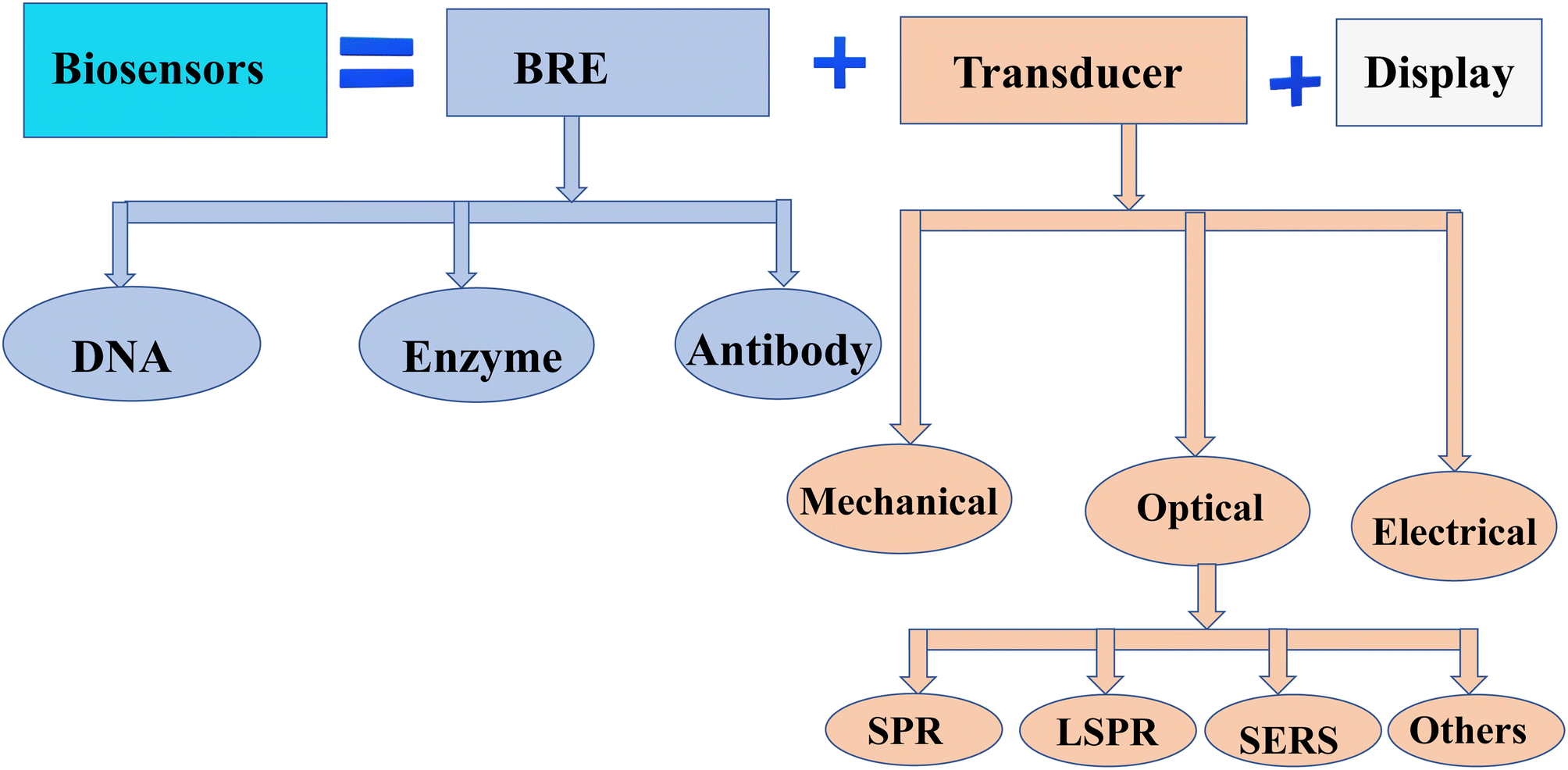 | ||
| Fig. 1 Schematic diagram of the classification of biosensors based on bioreceptors and transducers. | ||
In particular, optical biosensors combine the principles of optics and biochemistry to provide quantitative and qualitative information about the bio-recognition element, by measuring changes in absorbance, reflectance, luminescence, and fluorescence due to specific biomolecular interactions.17 The optical properties of plasmonic materials can be enhanced by controlling the design parameters of nanostructures like shape (nanospheres,18 nanorods,19 and nanopyramids), size (quantum dot,20 NPs,21 and micro22), composition, configuration, and environment of the nanostructures (optical fiber, grating, high-index prism, and waveguide). Plasmonic biosensors rely on the interaction of light with metallic nanostructures to detect and measure biological molecules. Therefore, the plasmonic biosensors typically operate based on the tuning of the plasmonic resonance through the interaction of light with metallic nanostructures.23 Energy loss in the layers can broaden the plasmonic resonance peaks, which can affect the accuracy and precision of the biosensor's measurements.24 Broadened peaks can make it more challenging to distinguish between different analytes or lead to false positive or false negative results.25 To mitigate the effects of energy loss in layers of plasmonic biosensors, optimization of layer thickness, and advanced fabrication techniques such as atomic layer deposition or chemical vapor deposition, can be used to create high-quality layers with reduced energy loss. These factors advance plasmonic biosensor performances over conventional ones allowing (i) label-free detection,26 (ii) real-time monitoring,27 (iii) high re-usability,28 and (iv) simple sample treatments.29 The disadvantages include (i) mass transportation limitations, (ii) non-specificity of the binding surface, (iii) steric hindrance during the binding event, and (iv) data misinterpretation.18,26,28
To overcome these limitations, nanophotonics community fabricated photonic crystals and plasmonic biosensors.30 Photonic crystals are periodic structures that have a specific refractive index pattern at the nanoscale size.31 Their optical properties, such as the photonic bandgap, cause light of certain wavelengths to be forbidden or highly confined within the structure.32 When biomolecules interact with the photonic crystal surface, they cause changes in the local refractive index, leading to alterations in the light propagation characteristics. These alterations can be measured as changes in the reflection or transmission of light, enabling the detection and analysis of biomolecular interactions and resulting in photonic crystal biosensors (PCB).33,34 The sensitivity of these biosensors is directly influenced by the overlap between the photonic bandgap of the sensor and the spectral range of the incident light or the wavelength at which the detection is performed.35
On the other hand, plasmonic biosensors utilize the unique optical properties of plasmonic materials, such as metallic nanoparticles or films, which support the excitation of surface plasmon polaritons (SPPs).36 SPPs are collective oscillations of free electrons at the metal–dielectric interface resulting from the coupling between the incident light and the metal surface. Binding interactions between the target molecules and the sensing surface cause measurable changes in the optical response, such as a shift in the wavelength or a change in the intensity of the reflected or scattered light.37 This allows for the detection and quantification of the analyte concentration or the binding events happening in real time. Based on their design, fabrication, and operation the plasmonic biosensors are classified into localized surface plasmon resonance (LSPR),38 plasmon-enhanced fluorescence (PEF),39 surface-accelerated Raman spectroscopy (SERS).40
Hybridization of photonic and plasmonic biosensors combines the strengths of plasmonic and photonic crystal biosensors to offer enhanced capabilities for sensing applications. The hybridization can involve incorporating plasmonic nanostructures into photonic crystal structures or utilizing plasmonic enhancements in conjunction with photonic crystal platforms.41 Some notable hybridization techniques include: plasmonic–photonic crystal nanoantennas, plasmonic–photonic crystal waveguides, and plasmonic–photonic crystal sensors42,43 with the core advantages of high sensitivity, specificity, real-time detection, label-free analysis, and the ability to measure multiple biomarkers simultaneously. This helps to detect a wide range of cancer biomarkers, including circulating tumor cells, DNA mutations, proteins, and microRNAs.44 However, like any diagnostic tool, the selection of the appropriate biomarker of interest, the sample type, and the required sensitivity and specificity are the main requirements. Currently, researchers continue to advance optical biosensing technologies, aiming to enhance the performance and wider clinical application in cancer diagnosis.
Therefore, in this review paper, we aim to provide an in-depth analysis of the major contributions and novelty in the fields of plasmonic biosensors, photonic crystal biosensors, and the hybridization of photonic and plasmonic biosensors. We explore the advancements in each biosensor type individually, including their working principles, advantages, and limitations. Furthermore, we discuss the recent breakthroughs in combining plasmonic and photonic components to create hybrid biosensors, which offer enhanced capabilities such as increased sensitivity, improved multiplexing, and precise control over excitation. The paper presents a comprehensive overview of the cutting-edge research, highlighting the novel approaches, innovative designs, and potential applications of these biosensing technologies. By understanding the major contributions and novelty in each area and exploring the opportunities and challenges in hybrid biosensors, this review paper provides valuable insights for researchers, engineers, and practitioners striving to advance biosensing technologies for various applications.
The rest of the work is organized as follows: Section 1 provides a general introduction to the topic, enriched by Section 2, which provides a broad and updated overview of modeling and experimental techniques for different classes of plasmonics. Section 3 gives a brief overview of different classes of photonic crystal biosensors, followed by Section 4, where we provide a broad and updated overview of plasmonic and photonic crystal hybridization techniques. And finally, Section 5 summarizes the whole discussion of the work.
2 Plasmonic biosensors for cancer diagnosis
Plasmonic biosensors (PBs) have gained significant attention in recent years due to their numerous advantages and advancements like: enhanced sensitivity and selectivity, label-free detection, and miniaturization and portability. These advancements have the potential to revolutionize diagnostics, enhance healthcare delivery, and contribute to scientific advancements in various fields. PBs are grouped into: those that use thin metallic films and individual inorganic plasmon resonant nanostructures.45 Within each class, there are many sensing modalities developed to provide extraordinary capabilities of high sensitivity, specificity, and real-time monitoring of biological analytes in the field of cancer diagnosis.46,47 Over the years, new sensing strategies and systems have been developed employing theoretical, experimental, and computational advancements.48–50Under theoretical advances such as finite-difference time-domain (FDTD),51 rigorous coupled-wave analysis (RCWA),52 boundary element methods (BEMs),53 and transfer matrix element (TME)54 methods have been applied to better understand and predict the optical properties and sensing performance of plasmonic structures. In addition, due to experimental advances, enhanced fabrication techniques (such as nanosphere lithography, electron beam lithography, and nanoimprint lithography) and improved surface functionalization have been developed considering temperature dependence coating to enable better reproducibility and scalability in biosensor fabrication.23 Temperature dependence of the coating affects the sensor's response by improving refractive index, signal stability, and establishing proper calibration and normalization.55,56 Furthermore, some computational advances are: high-performance computing, machine learning and data analytics have been applied to handle the large datasets generated by plasmonic biosensors. These techniques aid in the identification of specific binding events, noise reduction, and the extraction of valuable information from complex sensor responses.57 In the proceeding subsections, we review different classifications, experimental and theoretical designs, sensor and detection mechanisms, and limitations and future perspectives of recent plasmonic biosensors in detail.
2.1 Surface plasmonic resonance biosensors (SPRBs)
The interaction of incident photons at a certain angle of incidence with shiny MNPs (Ag, Au, Al, etc.) on a metallic surface (dielectric materials) resulted in, the collective oscillations of free electrons in a parallel direction to the metallic surface called surface plasmon61,62 as seen in Fig. 2. These can be explicitly explained in terms of before and after Brewster angle. Studying the SPRB behavior before the Brewster angle allows for maximizing the sensitivity and performing highly accurate molecular detection or quantification.63 And dealing after the Brewster angle can provide insights into the suppression mechanisms of surface plasmons and their potential use in applications where sensitivity requirements are different, such as in chip-based integrated systems or for refractive index determination.64 On the other hand, the interaction of resulted in surface plasmons with the biological sample generates an electric field (in the range of 100 to 600 nm) which is different from bare (without a biological sample).65 This phenomenon results in a surface plasmon resonance biosensor (SPRB). The advancement in standard components of SPRBs such as the light source, detector, coupling components (grating, prism, optical fiber and wave-guide) and imaging optical system leads to the use of SPRBs in applications ranging from environmental protection to medical services.66,67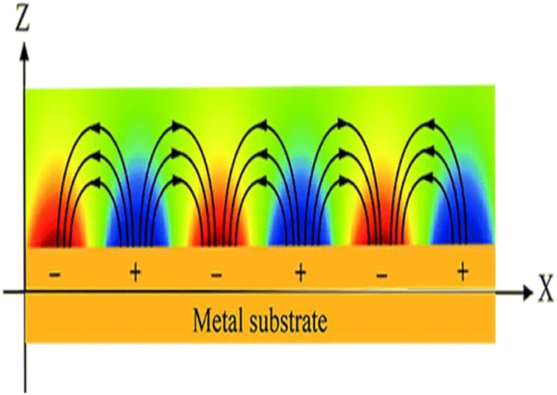 | ||
| Fig. 2 Schematics of surface plasmon resonance phenomena. This figure has been reproduced from ref. 58 with permission from the Royal Society of Chemistry, copyright 2020. | ||
Thus the first SPRB with the components of light, gratings, and dielectric materials was introduced in 1902 by R. W. Wood, which was applied to observe patterns of unusual dark and light bands in reflected light.68 Following, the theoretical formulation of MNP spectroscopy in dielectrics was given by J. C. Maxwell Garnett in 1904.69 In addition, the theoretical conclusion of surface plasmons supported by the network was given in 1941 by U. Fano.70 Furthermore, the excitation of surface waves on a metal-film surface with attenuated total reflection (ATR) techniques was simultaneously proved.71,72 These allow light to be confined below the diffraction limit and open up sub-wavelength photonic device integration.
Multiple factors influence the sensitivity of SPRBs; understanding these factors is crucial for optimizing the performance and achieving the desired sensitivity levels. For example (i) plasmonic structure design: factors such as the number of layers (sensitivity increases with the number of layers73,74), material composition (higher refractive index results in greater sensitivity75), and coatings (coating thickness, techniques, composition, stability, and functionalization methods should be considered to ensure efficient and specific analyte binding76), (ii) analyte concentration: lower detection limits and greater sensitivity can be achieved when lower concentrations of analytes can be reliably detected.74,77 (iii) Noise reduction: such as non-specific binding or fluctuations in the refractive index of the surrounding medium, can mask the sensor response and decrease sensitivity.76 (iv) Environmental factors: such as temperature, pH, humidity, and buffer composition can influence the performance and sensitivity of the biosensor.78 Considering these, it has followed that several modalities have been developed for a wide range of applications in different modalities (see Fig. 3).
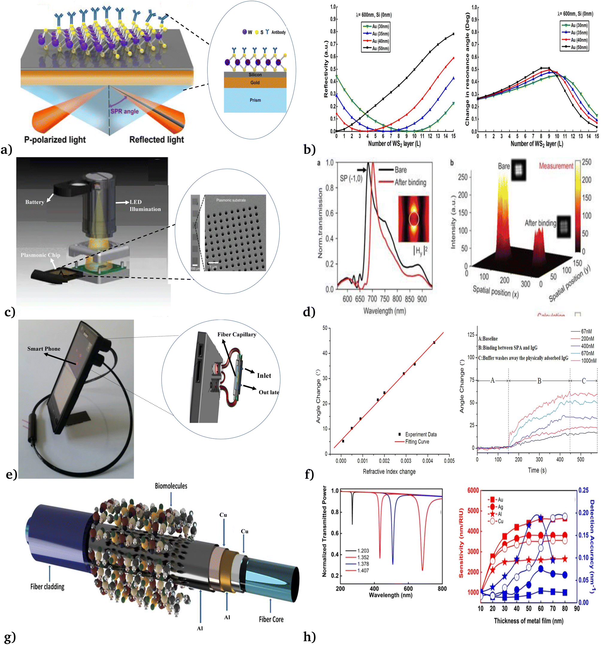 | ||
| Fig. 3 Different modalities of SPRB applied for the detection of cancer cells. (a & b) Prism-based SPR. This figure has been reproduced from ref. 46 with permission from Springer Nature, copyright 2016. (c & d) Plasmonic micro-arrays. This figure has been reproduced from ref. 49 with permission from Springer Nature, copyright 2014. (e & f) Fiber optic based. This figure has been reproduced from ref. 59 with permission from Springer Nature, copyright 2015. (g & h) Multi-layer metallic surface based. This figure has been reproduced from ref. 60 with permission from American Chemical Society, copyright 2021. | ||
Recently, Zeng et al.46 theoretically designed SPRBs using silicon nanosheets and two-dimensional transition metal dichalcogenides (Fig. 3a). Their configuration was governed by Fresnel equations and transfer matrix method in the visible and near-infrared wavelength range. From reflectivity spectra (Fig. 3(b)), the sensitivity, full width at half maximum, and much better performance than that of the conventional sensing scheme were observed. However, the scheme they developed was difficult to perform experimentally. Following this, Cetin et al.49 fabricated a compact optoelectronic sensor which was 7.5 cm tall and weighed 60 g (Fig. 3(c)) for high-throughput screening of biomolecular interactions. By employing pPlasmonic micro-arrays coupled with a lens-free computational imaging system, the diffraction patterns (Fig. 3(d)) of plasmonic nanostructures were recorded under uniform illumination using a single-light emitting diode tuned to the plasmonic mode of the nanoapertures. The fabricated label-free biosensor was applied for the quantitative detection of mono and bilayer proteins with a thickness of 3 nm only.
In addition, Liu et al.59 reported a more lightweight and cost-effective fiber optic SPRB made up of light-guiding silica capillary coated with a 50 nm gold film that linked with an easily removable smartphone case (see Fig. 3(e)). In this platform the phone case is used as a light source (LED flash) and detector (phone camera), to record the light intensity of different concentrations (Fig. 3(f)) of antibody binding every 0.5 seconds. However, the phone case and SPRB connector need more sophisticated Android application and hardware. Thus, to configure the relative merits of one configuration over the other, Radha et al.60 proposed a multi-layer metallic surface (Ag, Al, Au and Cu as seen in Fig. 3(g)) employing N-layer matrix formalism. Their work reveals that the use of Al/Cu/Al/Cu configuration provides the extraordinary (1433.82 RIU−1) figure of merit (FOM) (Fig. 3(h)) for detecting analytes with only refractive index in the range of 1.350 to 1.414.
In general, SPRBs detect alterations in the refractive index to assess molecules bound to a metal surface with rapid and real-time evaluation, excellent selectivity, and reproducible response. These characteristics render them an excellent approach for detecting potential markers in cancers.79 Despite these advances, some limitations of SPRB are (i) anything that alters the refractive index at the sensing surface will interfere with the analysis including nonhomogeneous (complex) sample matrices, and nonspecific binding interactions,80 (ii) the ligand may not maintain its native configuration upon immobilization on the sensor chip surface,81 and (iii) limited sensor area, leading to a diminished capacity.82
2.2 Localized surface plasmon resonance biosensors
When light and conductive nanoparticles interact, prominent spectrum absorption and significant electromagnetic near-field enhancements result.66 If the frequency of incident light matches with the frequency of the collective movement of the near field, the strongly localized oscillation of surface electrons in the range of 50 to 100 nm resulted83 as shown in Fig. 4. This phenomenon is called localized surface plasmon resonance (LSPR). Due to resonance conditions in LSPR being higher than that of SPR, LSPR-based biosensors are more responsive than those of SPRBs.67 Therefore, LSPR-based biosensors have high-sensitivity and high-resolution imaging.84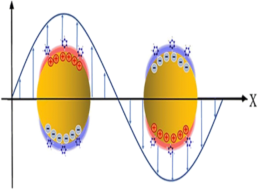 | ||
| Fig. 4 Schematics of localized surface plasmon resonance. This figure has been reproduced from ref. 58 with permission from the Royal Society of Chemistry, copyright 2020. | ||
There are two main sensor modes under LSPR: the first is wavelength-shift sensing, which tracks the light wavelengths that cause the collective oscillation using UV-Vis spectroscopy.58 The variations in the wavelength extinction curves can be used to monitor changes in the refractive index caused by the adsorption of the target analyte. The second method relies on the emergence of stronger electromagnetic fields that emanate from the nonstructural surface.85
Recently, employing the phenomena of LSPR, Chang et al.50 demonstrated the bio-compatible, highly sensitive and responsive metal–insulator–metal nanodisks sensors (see Fig. 5(a) and (b)) that were applied to detect A549 cancer cells in different solutions. Their experimental investigation shows the new development of on-chip microfluidic biosensors for the detection of cancer cells on polar and nonplanar surfaces. Besides, Huang et al.58 utilized an automated microfluidic-based LSPR biosensor for multiplex inflammatory biomarker detection under different reagent conditions (see Fig. 5(c) and (d)). They report rapid, multiplex, and multiparallel continuous inflammatory biomarker detection, which would be beneficial for various medical applications. Moreover, Nan et al.86 manufactured a wearable LSPR-based biosensor by depositing gold nanoparticle (AuNP) layers on a 3-aminopropyltriethoxysilane (APTES)-functionalized poly(dimethylsiloxane) (PDMS) substrate, to detect cortisol levels in the human body (see Fig. 5(e) and (f)). Their newly reported biosensor exhibited (i) excellent detection ability in cortisol solutions of various concentrations ranging from 0.1 to 1000 nM with a detection limit of 0.1 nM, (ii) good stability under various mechanical deformations, and (iii) measured cortisol levels in different environmental setups.
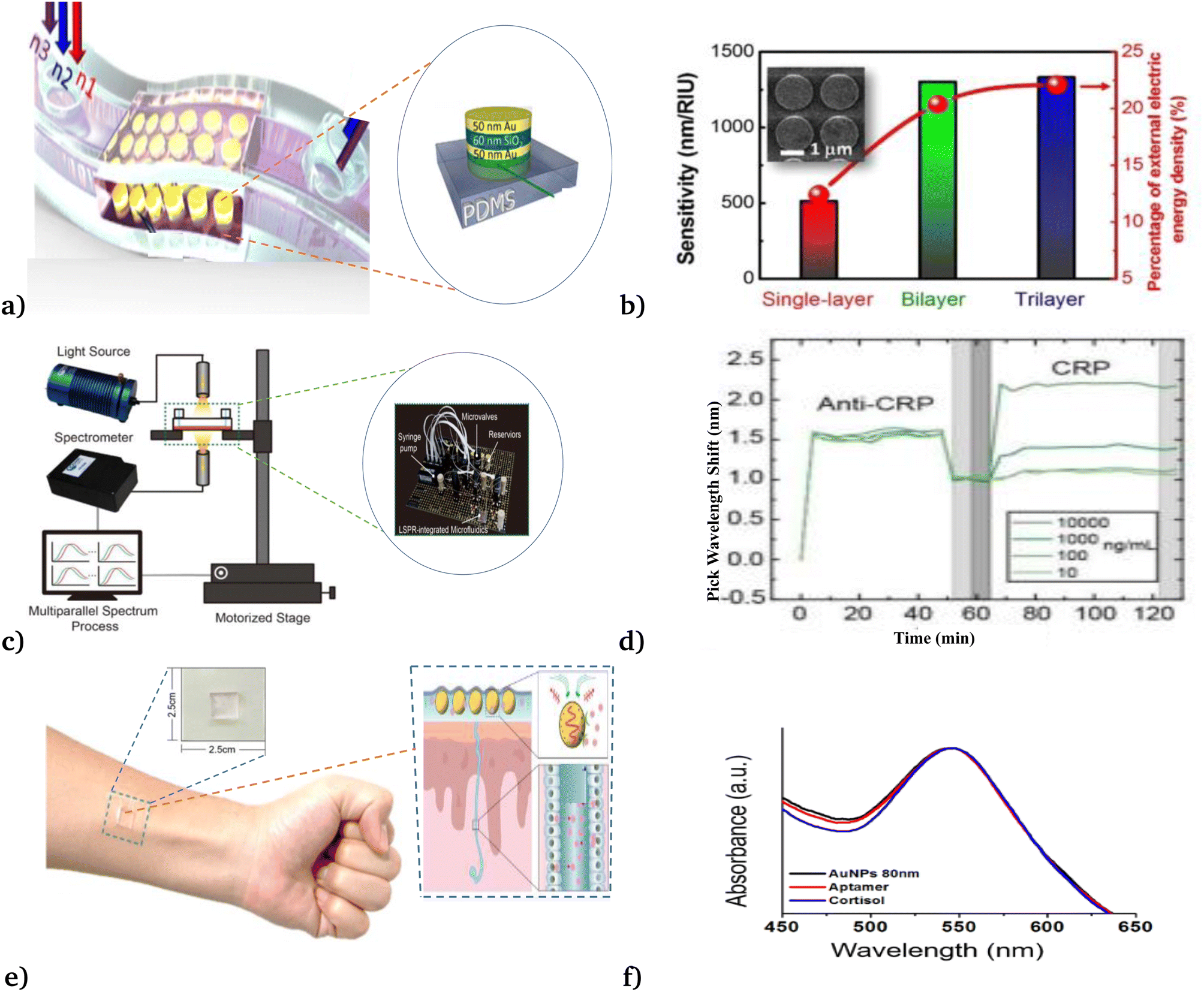 | ||
| Fig. 5 Different modalities of LSPR applied for the detection of cancer cells. (a & b) Metal–insulator–metal nanodisk-based LSPR biosensor. This figure has been reproduced from ref. 46 with permission from Springer Nature, copyright 2018. (c & d) Microfluidic-based LSPR biosensor. This figure has been reproduced from ref. 58 with permission from the Royal Society of Chemistry, copyright 2020. (e & f) Wearable LSPR-based biosensor. This figure has been reproduced from ref. 86 with permission from MDPI, copyright 2023. | ||
To this end, the LSPR biosensor has the following inherent advantages because of the small size of a localized plasmon evanescent field, it can be carried out with straightforward instrumentation, room light, and the human eye is sufficient to observe some of the reactions; sensor chips for the instrument can be produced at a more affordable price, user-friendly, and easier to use and maintain.85,87 Some basic disadvantages are: (i) the linearity of LSPR biosensors is highly affected by the optical properties of colloid NPs, this enforced to use of only shiny MNPs like Au.88 (ii) The sensitivity is highly affected by a combination method of target chemicals and chromogenic reagents; this requires reasonable sample preparations.89 (iii) The selectivity of such biosensors is dependent on the type, concentration, and preparation method of analytes.90
2.3 Surface-enhanced Raman spectroscopy
The interaction of photons with molecules resulted in either elastic (Rayleigh), or inelastic (Raman) scattering.94 As a result of this interaction, photons may gain energy from a molecule that undergoes the opposite process (anti-Stokes Raman scattering) or lose energy in favor of a molecule that advances from the ground state to its first excited vibrational state (Stokes Raman scattering).48 And the in-elastically scattered photons contain information on the vibrational modes of the molecules they interact with95 as seen in Fig. 6. For the first time, these phenomena were observed in 1974 by Fleischmann who reported an unexpectedly large Raman signal from pyridine adsorbed on a roughened silver electrode.96 Following, Jeanmaire and van Duyne and Albrecht and Creighton confirmed Fleishman's findings and hypothesized that this phenomenon originated from strong electrochemical electric fields at the metal surface (Jeanmaire) or by the formation of a molecule–metal complex (Albrecht); lately, Moskovits proposed that the large signal originated from the optical excitation of collective oscillations of the electrons in the metallic nanosized features at the surface.97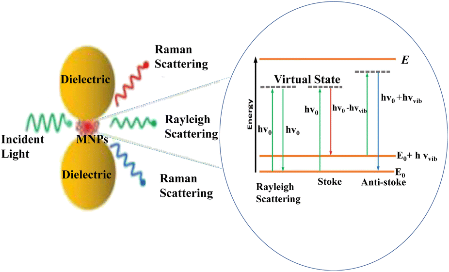 | ||
| Fig. 6 Schematic diagram of the general phenomena of SERS. This figure has been reproduced from ref. 91 with permission from American Chemical Society, copyright 2018. | ||
Employing the above progress, Xu et al.48 designed a graphene-mediated SERS substrate to result in electromagnetic “hot” spot signals (Fig. 7(a) and (b)). These signals are free from various metal–molecule interactions and are more stable against photo-induced damage and have interesting advantages over normal SERS. Thus, their work enables direct, real-time and reliable detection of trace amounts of analytes in various systems, with high efficiency and universality of analysis substrates. In addition, Polavarapu et al.92 with high motivation in recent advances in conductive ink pens for electronic devices on paper (Fig. 7(c) and (d)), presented a simple “pen-on-paper”-based SERS substrate. The proposed “pen-on-paper” substrate writes SERS arrays using plasmonic inks (made of silver nanospheres, gold nanospheres, and gold nanorods), that can be used with various excitation wavelengths. Their method offers cost-effective, portable, and efficient SERS substrates for point of care applications.
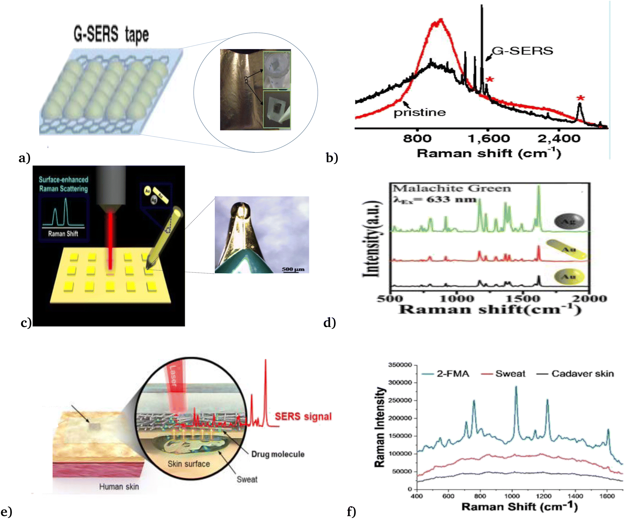 | ||
| Fig. 7 Recently developed SER biosensor. (a) Graphene mediated SER biosensor, and (b) spectra of the graphene-based SER biosensor. This figure has been reproduced from ref. 48 with permission from PNAS, copyright 2012. (c) Pen-on-paper-based SER biosensor and (d) performance analysis of the pen-on-paper-based SER biosensor with different nanoparticle types, shapes, and sizes. This figure has been reproduced from ref. 92 with permission from the Royal Society of Chemistry, copyright 2014. (e) Wearable SER biosensor and (f) spectra of the wearable SER biosensor. This figure has been reproduced from ref. 93 with permission from American Chemical Society, copyright 2021. | ||
Recently, Jung et al.93 reported a wearable surface-enhanced Raman scattering (SERS) sensor, as seen in Fig. 7(e) and (f). That constituted of a SERS active layer, dermal protecting layer (prevents damage and contaminations), silk fibroin protein film layer (absorbs aqueous solutions and filtrate molecules larger than the nanopores), plasmonic silver nanowire (to enhance the Raman signal of the molecules that penetrated through the SERS patch), and transparent dermal protecting layer (allows laser penetration to the plasmonic layer to enable Raman measurement through the SERS patch without its detachment from the surface). They investigated the feasibility of the proposed wearable SERS biosensor by applying it for drug detection on the human cadaver skin.
Moreover, Cetin et al.,49 presented a wearable plasmonic–electronic sensor by using a thin layer of a hydrogel loaded with sweat gland secretion molecules (acetylcholine chloride) that stimulate sweat gland secretions, which were attached to two spiral fractal mesh electrodes (see Fig. 7(e) and (f)). The fabricated biosensor successfully monitored the variation of trace amounts of drugs inside the body and obtained an individual's drug metabolic profile. These solve the existing gap in wearable sensing technology by providing a universal, sensitive molecular tracking means to assess human health.
Indeed, SERS shows a broad range of advantages: (i) possible unique fingerprint signature of the analyte causing high selectivity,92 (ii) easy sample preparation method,95 (iii) no signal interference from the analyte medium, which is usually water-based, (iv) single-molecule detection,93 (v) potential for multiplexed sensing with a single laser beam, (vi) high throughput, and (vii) POC applicability by using commercially available portable Raman probes.92
2.4 Plasmonic biosensors: cancer detection mechanism and performance analysis
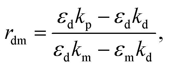
Plasmonic biosensors are optical sensing devices that utilize the interaction of light with surface plasmons, which are collective oscillations of free electrons or electric field distribution at the metal–dielectric interface. To derive the electric field distribution, Maxwell's equations and appropriate boundary conditions were applied. By considering a plane wave incident normally from the dielectric side onto the metal–dielectric interface, the electric field distribution in the structure can be described by an incident field (Einc = E0![[thin space (1/6-em)]](https://www.rsc.org/images/entities/char_2009.gif) e(−ikd × z) for E0 is the incident field amplitude, k is the wavevector, and d is the thickness of the dielectric substrate), a transmitted field (Etra = Etra = t × Eince(−ikm × z), where t is the transmission coefficient and m = k2 − k1 = (2π/λ) × (n2 − n1) represents the parallel wave vector component. And for the transmitted field, we can use Snell's law to relate the angle of incidence (θ1) and the angle of transmission (θ2)) sin(θ1)/sin(θ2) = n1/n2, and a reflected field (Eref = r × Einc, where r is reflection coefficient). Using the boundary conditions, we can relate the electric field components at the interface as
e(−ikd × z) for E0 is the incident field amplitude, k is the wavevector, and d is the thickness of the dielectric substrate), a transmitted field (Etra = Etra = t × Eince(−ikm × z), where t is the transmission coefficient and m = k2 − k1 = (2π/λ) × (n2 − n1) represents the parallel wave vector component. And for the transmitted field, we can use Snell's law to relate the angle of incidence (θ1) and the angle of transmission (θ2)) sin(θ1)/sin(θ2) = n1/n2, and a reflected field (Eref = r × Einc, where r is reflection coefficient). Using the boundary conditions, we can relate the electric field components at the interface as| Ez(z = d) = Etra + Eref = Einc + ΓSPPESPPT. | (1) |
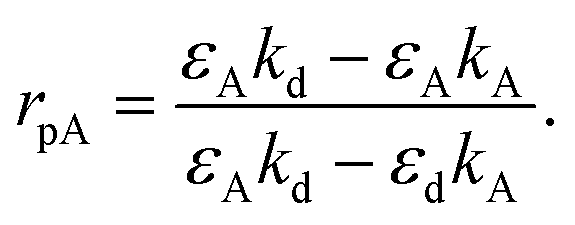
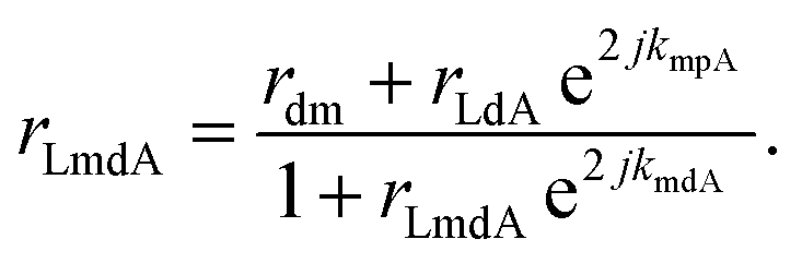
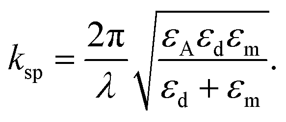
The recognition material (antibodies) was crucial in identifying the cancer biomarker for biosensors.11 The antibodies are created as a substance with an affinity that can also be employed as an analyte for detection purposes. Furthermore, these antibodies are applied to target any cancer biomarkers.46 In addition, to identify and more precisely profile different types of cancer, CTCs and ctDNA offer deeper insight into the dynamic oscillations and traits of the tumor disease. Their insufficient quantity and inherent heterogeneity make detecting CTCs and ctDNA more challenging. Thus, several photonic device integration methods should be dispersed for effective illness detection methods: intensity, wavelength, angle, and phase-interrogated devices to generate SPPs. The benefit of using angle interrogation is that it offers a high signal-to-noise ratio (SNR) and a single source of input radiation. With this consideration the reflectance of laser light from nanosurface and biological molecule (gene) interaction mathematically given by eqn (2) to eqn (4) as98 interaction takes the form,99
 | (2) |
 | (3) |
 | (4) |
The overall reflection coefficient of the output field is discussed employing eqn (2) to (4) as
 | (5) |
In addition, the propagation constant of resulting biosignals takes the form100
 | (6) |
Employing eqn (5) the performance analysis of plasmonic biosensor in angle interrogation modalities are defined by100 full width at half maximum 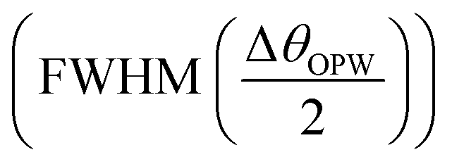 , sensitivity
 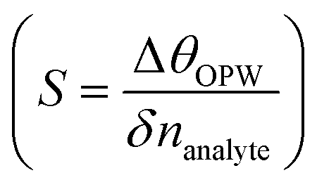 for Δnanlayte is changed in the refractive index of analyte, figure of merit
 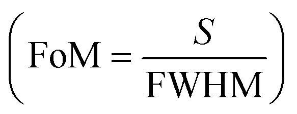 , detection accuracy
 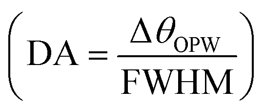 , limit of detection
 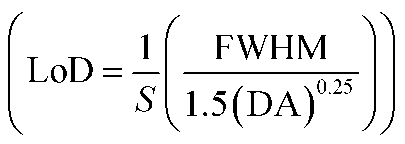 , and resolution (R = LoD × S). In addition, for wavelength interrogation, the performance analysis is discussed in ref. 77 as: full width at half maximum
 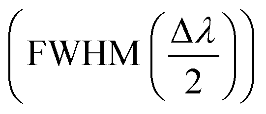 , and sensitivity
 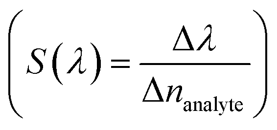 101 of the proposed biosensor are outpaced. Here Δλ and Δnanalyte are changes in the refractive index of the resonance peak and biomolecules, respectively. Besides, the figure of merit (FOM) is also given as the ratio of sensitivity to FWHM,102 and resolution
 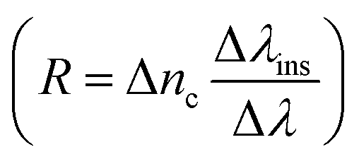 ,50,103 for, Δλins is the resolution of instrumental peak wavelength.
3 Photonic crystal-based biosensors for cancer diagnosis
Electron–electron interactions and electron–phonon scattering in real materials were first understood by Anderson and Mott's observations of electronic localization in disordered solids. The concept provided the basis for understanding the strong localization of photons in certain disordered dielectric superlattices104,105 and raised the concept of the fabrication of photonic crystals.106 Photonic crystals (PCs) are photonic structures fabricated or designed using the periodic arrangement of dielectric materials, in either the micro-structure107 or non-structural shape (in 1D, 2D, and 3D) in repeating fashions to guide light wave propagation into very strong confinement.108 PC structures appear in a variety of geometries, like slabs, colloids, Bragg reflectors, microcavities, and opals. The optical phenomenon of those structures is explained in terms of simple Bragg structure, a detailed description is given in Fig. 8.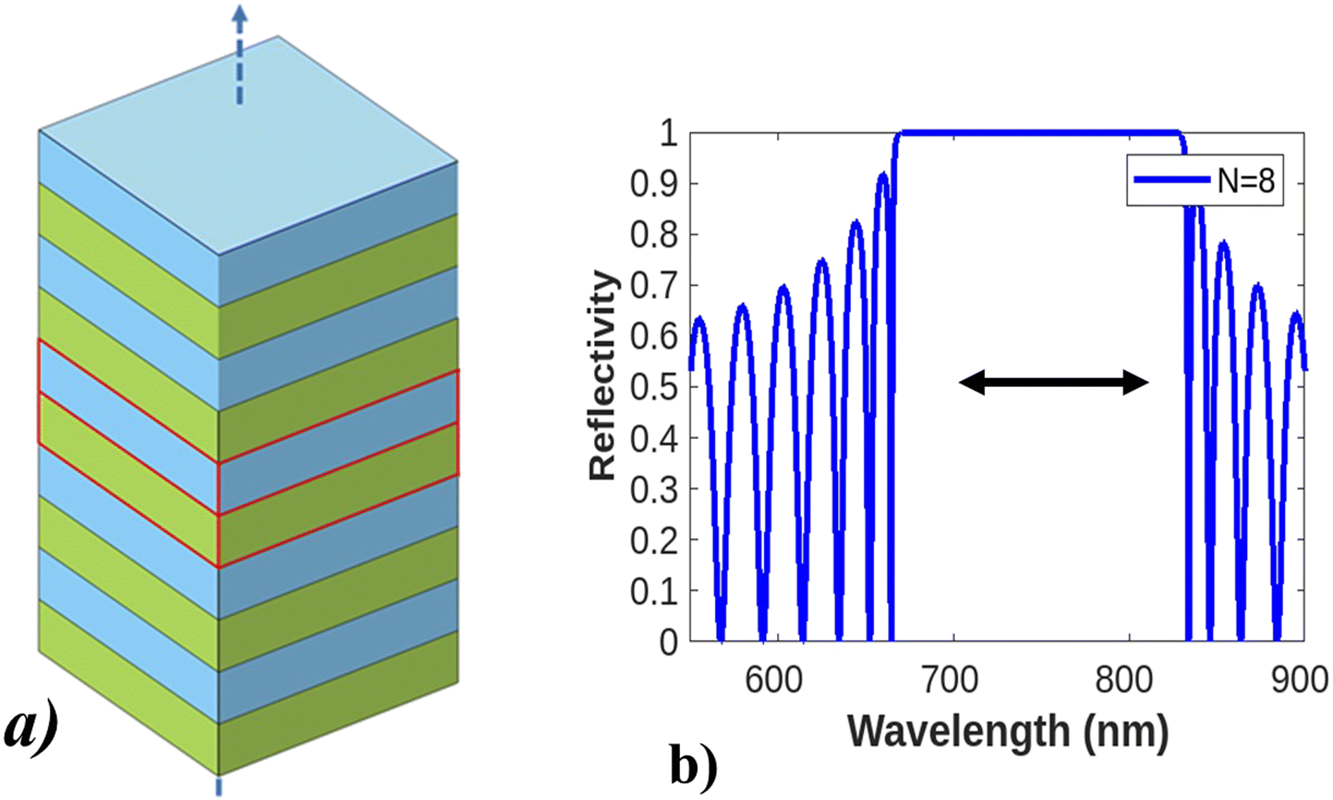 | ||
| Fig. 8 Design and optical phenomena of a photonic crystal. (a) Shows the design of photonic crystals with a different arrangement of dielectric layers having a low and high refractive index, photonic crystal–light interaction, and how light behaves. (b) Shows a Bragg reflector with broad photonic band gap reflection spectra. This figure has been reproduced from ref. 109 with permission from IEEE, copyright 2002. | ||
Photonic crystals may exhibit resonance shifts or modifications due to changes in the interaction between incident light and the crystal structure. Studying photonic crystals' interaction with light before and after the Brewster angle can facilitate the exploration of enhanced light control, such as low reflection, transmission filtering, or waveguiding effects. These properties can be advantageous for designing optical devices, including sensors, lasers, or modulators by allowing the confinement of light into the nanoscale range owing to the existence of a photonic band gap in which light propagation is forbidden.110 This band gap can be modified using either line or point defects to control the flow of input light and decide the direction of propagation.111 As a result, photonic crystals can be applied to quantum technologies,112 optomechanics,113 photonics,114 optoelectronics,115 signal processing,116 and many other fields. Examples include gas photonic papers,117 reflective flat displays,118 inkless printing,119 and sensing. Specifically, the application of PC for point of care application has attracted considerable attention and is dispensed in waveguide and cavity-coupled modes.
3.1 Wave guide-based PC biosensors
Photonic crystal–light interaction causes extraordinary light reflection that depends on the period and the effective refractive index (mλ = 2neffd).122,123 For m, λ, neff, and d are the diffraction order, wavelength of the reflected light, effective refractive index of the periodic structure, and the lattice period of the crystal, respectively. On the other hand, based on the exact periodic modulation, PC may possess a photonic band gap (PBG).124 Thus many pioneers introduced PC waveguides (PCWs) to allow the propagation of a narrow range of wavelengths within the photonic band gap range.111Thus, Kassa et al.120 investigated the slotted PCW with a triangular lattice pattern of ring-shaped holes (see Fig. 9(a) and (b)) at mid-infrared wavelengths. The 3D simulation results show that the proposed guide geometry leads to a very high sensitivity (device insertion loss level of 3 dB), is highly affected by variations in the ambient environment index, and varies with opto-geometric factors. Following, Torrijos et al.121 fabricated a silicon structure surrounded by a silica cladding PCW with two single-mode waveguides at the input/output ports that result in polarization electromagnetic mode and a rectangular taper between the uniform and periodic bimodal parts (see Fig. 9(c) and (d)), to exhibit a large group velocity difference for optical path reduction. The results revealed that the single-channel bimodal periodic structure was highly recommended for optical interferometers, slow light regime results in higher phase-shift sensitivity, and high sensing operation (104 2 rad RIU−1 cm−1) for different ethanol dilutions in DIW are reported.
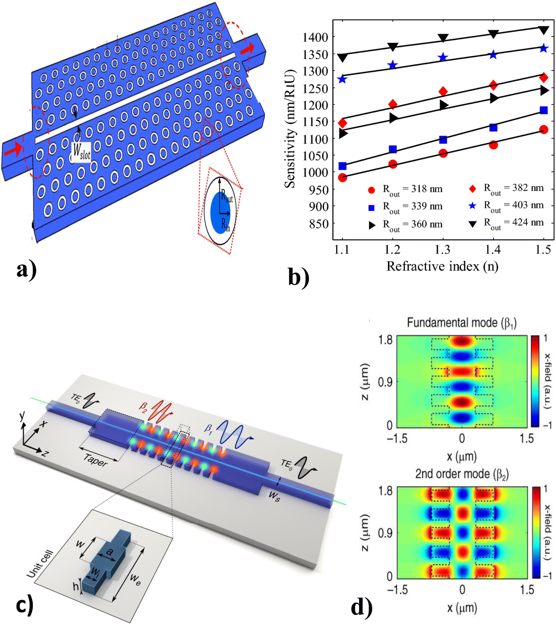 | ||
| Fig. 9 Different modalities of a PCW biosensor. (a) Slotted PCW with ring-shaped hole, and (b) sensitivity analysis of slotted PCW under different refractive indices. This figure has been reproduced from ref. 120 with permission from Springer Nature, copyright 2019. (c) PCW with two single-mode waveguides, and (d) fundamental and second-order mode field of PCW. This figure has been reproduced from ref. 121 with permission from Springer Nature, copyright 2021. | ||
3.2 Cavity-coupled PC biosensors
Engineering of light–matter interaction using quantum emitters attracts many scientific communities because of their potential application in quantum optics, quantum information processing, sensors, etc.127 Specifically, the realization of effective PC sensors requires either removing or changing the size and shape of given optical materials. Thus, PC cavities (PCCs) are engineered by creating local defects on the lattice geometry of periodic PC structures and/or by breaking the completeness of the PC band gap, to result in light confinement into very small areas that are capable of strong light–sample interactions 128 This has potential for lab-on-a-chip optical sensing applications along with the possibility of achieving high quality factors.With these considerations, Kim et al.,125 engineered high-quality factor-suspended PCC using hexagonal boron nitride (Fig. 10(a)). Following the procedures of (i) highly crystalline hBN flakes were exfoliated from sticky tape, and deposited onto trenched silicon substrates, (ii) tape residuals were removed by calcination in air for 2 h at 450 °C on a hot plate, (iii) desorption of contaminants and an increase of adhesion of flakes to the substrate were achieved by annealing in a tube furnace with argon at 850 °C for 30 min, (iv) by employing the EBIE etching method, a tungsten film was deposited in a homebuilt plasma sputter deposition chamber, (v) using focused ion beam (FIB) the cavities were fabricated, and (vi) finally, optical measurements were performed (Fig. 10(b)).
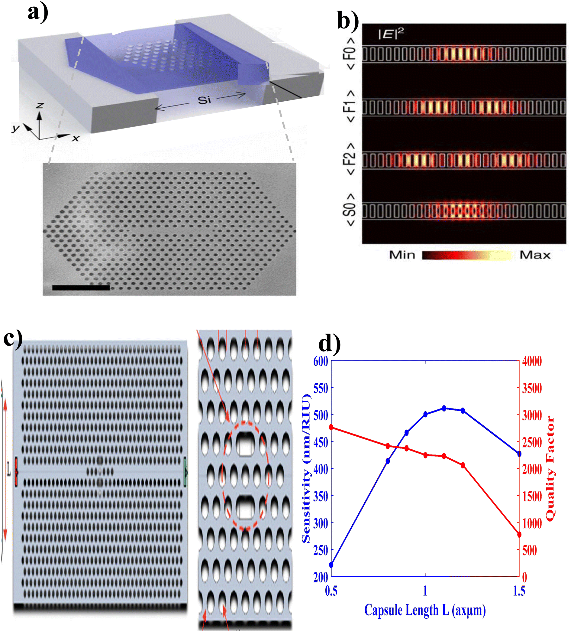 | ||
| Fig. 10 Cavity coupled PC biosensor. (a) Suspended PCC with hexagonal boron nitride. (b) FDTD spectra of suspended PCC. This figure has been reproduced from ref. 125 with permission from Springer Nature, copyright 2018. (c) Capsule-shaped PCC. (d) Performance analysis of capsule-shaped PCC. This figure has been reproduced from ref. 126 with permission from MDPI, copyright 2023. | ||
In addition, Maache et al.126 fabricated a capsule-shaped PCC (Fig. 10(c)) sensor for glucose concentration detection based on the change in refractive index (RI) with a sample infiltrated into the cavity. They reported a sufficient and efficient detecting PCC sensor with a high sensitivity (546.72 nm RIU−1), quality factor (2066.24), a low detection limit (1.44 × 10⁴ RIU), and high transmission value (97%) (Fig. 10(d)).
4 Hybridization of plasmonic and photonic crystals
The interaction between photons and plasmons allows for strong light–matter interactions, leading to enhanced light confinement and manipulation at the nanoscale. This is achieved by incorporating metallic nanostructures, such as nanowires or nanorods, into a periodic dielectric or semiconductor matrix. The metallic nanostructures support surface plasmon polaritons (SPPs), which are hybrid resonances of electromagnetic waves and collective electron oscillations at the metal–dielectric interface. Thus, hybrid plasmonic and photonic crystal biosensors (plasmonic–photonic crystals (PPCBs)) are engineered structures that combine the properties of both plasmonics and photonic crystals.132 These structures are designed to control and manipulate the propagation of both photons and plasmons simultaneously, offering unique opportunities for various applications. In PPCBs, the periodicity is achieved along one dimension.The periodic arrangement of metallic and dielectric components in 1D plasmonic PCs leads to the formation of band gaps, also known as photonic band gaps, where certain frequency ranges are forbidden for photon propagation. These band gaps can be tuned by adjusting the geometric parameters of the nanostructures, such as the size, shape, and periodicity. By controlling the band gap, plasmonic PCs allow for efficient light manipulation, such as guiding, filtering, and trapping of light in nanoscale devices for applications in sensing, imaging, and integrated photonics. The introduction of metal–dielectric layers over plasmonic materials has allowed light manipulation at subwavelengths and beyond diffraction limits due to its integration capabilities with other components such as splitters, waveguides, logic gates, switches, and filters.45–47 Before and after the Brewster angle, the hybrid functionality can allow for optimizing light–matter interactions, incorporating angle-dependent effects, and enhancing sensitivity or selectivity (Table 1).
| Methods | Layer order | FoM | LoD | Sensitivity | Reference |
|---|---|---|---|---|---|
| SPRB | Analyte/Fe2O3/Ag/prism | — | 0.17 (degree) | 365 (degree per RIU) | 74 |
| Ag-TiSi2-BP | 45.26 (RIU−1) | 0.21 (degree) | 218.6 (degree per RIU) | 133 | |
| CaF2/TiO2/Ag/BP/graphite | 87.95 (RIU−1) | 0.464 (degree) | 390 (degree per RIU) | 134 | |
| Prism/Ag/AlAs/TIBr/BP | 79.72 (RIU−1) | — | 475 (degree per RIU) | 135 | |
| PCB | Silicon road with air | 612.95 (RIU−1) | — | 263.57 (nm RIU−1) | 136 |
| Silicon PC/hexagonal cavity | 980 (nm RIU−1) | — | 915.75 (nm RIU−1) | 137 | |
| 5 × 5 silicon rods/air | 99.765 (RIU−1) | — | 2360.12 (nm RIU−1) | 138 | |
| PPCB | Ag/air/GaAs | 60.1 (RIU−1) | — | 714.3 (nm RIU−1) | 137 |
| Si-PC/Ag/SiO2/analyte | 2388 (RIU−1) | — | 1672 (nm RIU−1) | 131 | |
| Nested circular metallic split-ring resonators | 2083 (RIU−1) | — | 1250 (nm RIU−1) | 139 |
PPCBs can find applications in biological sensing, integrated optics, or optoelectronic devices, where the combination of resonance phenomena, surface plasmons, and photonic bandgap engineering is crucial.140 However, the high dissipation rate limits their application.82 Also, the PC guides the propagation of light waves to very tight confinement, which minimizes coupling losses, operating bandwidth, and tuning modes. As a result, PC-based biosensors are only capable of detecting analytes in a small area.104,105 Thus, several solutions to this problem were outpaced recently as, (i) search for novel materials with a lower dissipation, (ii) utilization of the SPP modes of interaction in multi-interface systems to result in the excitation of long-range SPPs, (iii) engineering several channels of SPPs, and (iv) hybridization of nanomaterials with photonic and plasmonic properties.
Recently, several hybridization mechanisms have been outpaced. For example, Sosnova et al.129 gave a brief theoretical demonstration of the hybrid plasmonic guided 1D PC based on a Bragg mirror (Fig. 11(a)). The simulation results showed that the hybrid P-PC mode resulted in low broadening (Fig. 11(b)) due to the redistribution of the electric field intensity between the photonic mode and SPP. These results were three times the Q-factor than for SPP-based biosensors of similar structures without a Bragg mirror. In addition, Koryukin et al.130 investigated the light transmission of hybrid Tamm-surface plasmonic–photonic mode in 1D and 3D configurations. They used the opal-like photonic crystal made up of Au layers with an FCC lattice to connect individual dielectric spheres on the surface of PC (Fig. 11(c)). The simulation of the transmission spectra was obtained using various parameters in the finite-difference time-domain (FDTD) method. Their result depicted that the transmission spectra of one-dimensional plasmonic–photonic crystals were maximum inside the photonic bandgap due to excitation of TPPs and 3D opal-like plasmonic–photonic crystals have no transmission peak in the bandgap due to unconventional Tamm state. Furthermore, Hajshahvaladi et al.131 designed hybrid plasmonic–photonic crystals (P-PhC) using metallic rods embedded in a rod-type photonic crystal (PhC) structure (Fig. 11(e)). From numerical simulations of the FDTD method (Fig. 11(f)), they reported the use of metallic rods in the coupling regions between waveguides and the resonant cavity significantly increases the interaction of the optical field and analyte inside the cavity, these results in high Q-factor (sensitivity of 1672 nm RIU−1 and figure of merit (FoM) of 2388 RIU−1) at optical communication wavelengths.
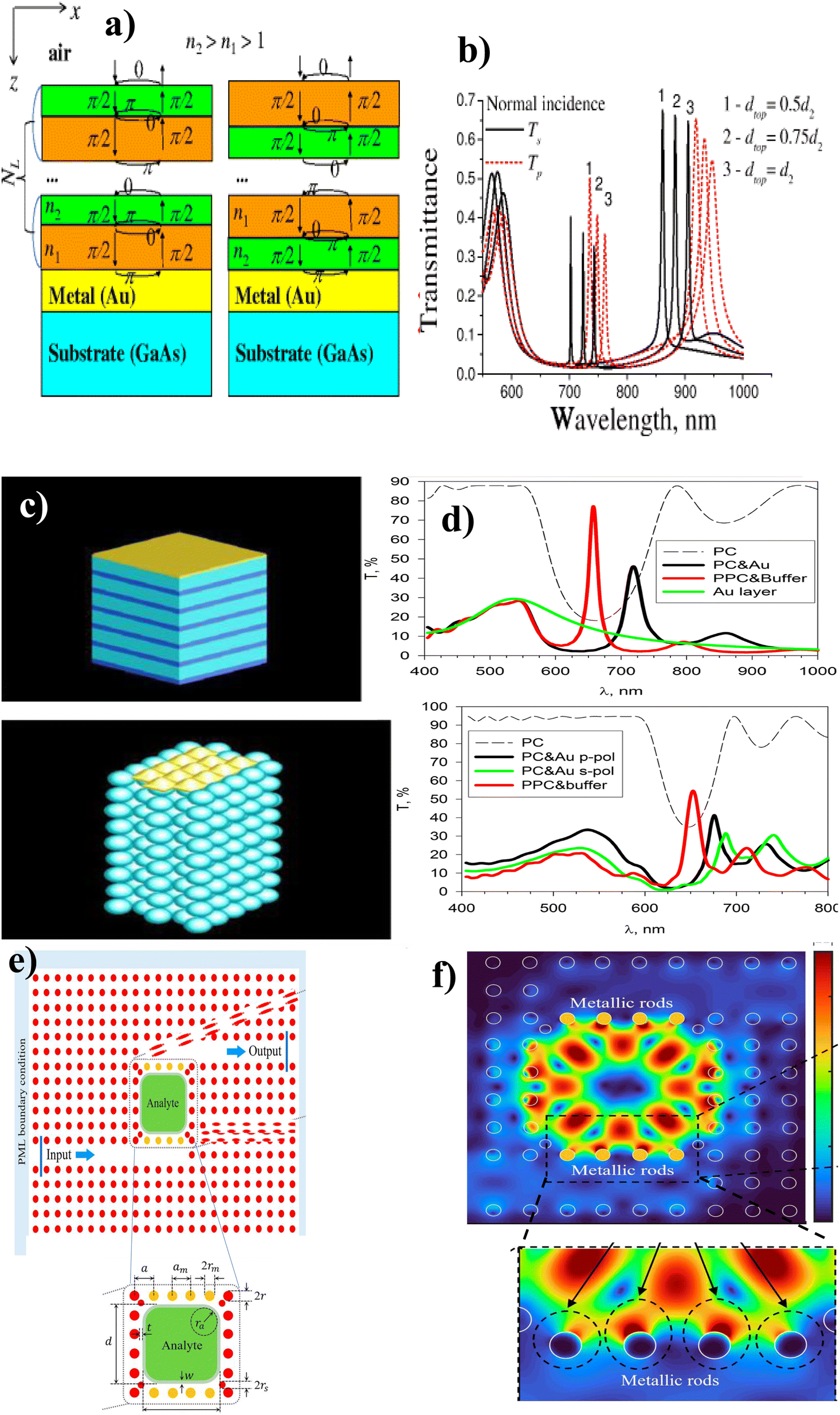 | ||
| Fig. 11 Hybridization of the plasmonic and photonic crystals. (a) Model of Bragg mirror in different alternating orders, and (b) S and P-polarized light spectra. This figure has been reproduced from ref. 129 with permission from Springer Nature, copyright 2016. (c) 1D and 3D opal-like photonic crystals made up of Au layers with an FCC lattice and (d) transmission spectra of 1D and 3D opal-like photonic crystals. This figure has been reproduced from ref. 130 with permission from Springer Nature, copyright 2019. (e) Metallic rods embedded in a rod-type photonic crystal and (f) FDTD simulation spectra. This figure has been reproduced from ref. 131 with permission from Springer Nature, copyright 2022. | ||
5 Conclusion
In this review, we have investigated the current status and future potential of the fundamental physics of light–matter interaction and advanced techniques for engineering light to sub-wavelength scales. Our focus has been on theoretical and experimental aspects of various biosensor technologies, including SPP, LSPP, SERs, PCW, and PCC, with specific applications in cancer diagnosis. We have emphasized the state-of-the-art modeling methods and experimental techniques developed in the past decade to uncover the intricate interaction of light with nanostructured optical materials, such as noble metals, highly doped semiconductors, and hybrid plasmonic–photonic crystal materials. Through the presentation of recent studies, we have demonstrated the advancements in understanding light–matter interaction with exceptional spatial and temporal resolutions. This knowledge is crucial for the future development of highly functional and effective optical biosensors by enabling precise measurements and a deeper understanding of the ultrafast response of plasmonic materials at the nanoscale.Furthermore, exploration of nanofabrication techniques can enhance the design and fabrication of biosensors with improved sensitivity and selectivity for specific cancer biomarkers. Integrating multiplexing capabilities can enable simultaneous detection of multiple biomarkers, enhancing diagnostic accuracy. The integration of plasmonic–photonic crystal biosensors with microfluidic technologies can lead to miniaturized devices for point-of-care diagnostics. Clinical validation studies are crucial to assess performance and reliability. Additionally, integrating artificial intelligence and machine learning algorithms can enhance data analysis and interpretation, enabling automated and more accurate cancer diagnosis. By pursuing these research avenues, plasmonic–photonic crystal biosensors have the potential to revolutionize cancer diagnosis, enabling earlier detection and personalized treatment approaches.
Conflicts of interest
The authors declare that they have no known competing financial interests or personal relationships that could have appeared to influence the work reported in this paper.Notes and references
- R. B. Kargbo, KRAS Inhibitors and Target Engagement Technology: From Undruggable to Druggable Targets in Cancer Therapeutics, 2022 Search PubMed.
- M. S. Alam, A. Sultana, M. S. Reza, M. Amanullah, S. R. Kabir and M. N. H. Mollah, PLoS One, 2022, 17(5), e0268967 CrossRef CAS PubMed.
- A. A. Pazzi, P. Vij, N. Salhadar, E. George and M. K. Tripathi, RNA Therapeutics-History, Design, Manufacturing, and Applications, IntechOpen, 2023 Search PubMed.
- A. Tavallaii, K. T. Meybodi, F. Nejat and Z. Habibi, World Neurosurg., 2023, 174, 74–80 CrossRef PubMed.
- P. Roy and B. Saikia, Indian J. Cancer, 2016, 53, 441–442 CrossRef CAS PubMed.
- T. Wasilewski, N. F. Brito, B. Szulczyński, M. Wojciechowski, N. Buda, A. C. A. Melo, W. Kamysz and J. Gębicki, TrAC, Trends Anal. Chem., 2022, 150, 116599 CrossRef CAS.
- S. Weng, D. Lin, S. Lai, H. Tao, T. Chen, M. Peng, S. Qiu and S. Feng, Biosens. Bioelectron., 2022, 208, 114236 CrossRef CAS PubMed.
- L. Tang, J. Yang, Y. Wang and R. Deng, ACS Sens., 2023, 8, 956–973 CrossRef CAS PubMed.
- D. Caballero, R. L. Reis and S. C. Kundu, Microfluidics and Biosensors in Cancer Research: Applications in Cancer Modeling and Theranostics, Springer, 2022, pp. 81–112 Search PubMed.
- C. Dincer, P. Chandra and E. Morales-Narváez, Front. Bioeng. Biotechnol., 2022, 10, 1008603 CrossRef PubMed.
- A. Singh, A. Sharma, A. Ahmed, A. K. Sundramoorthy, H. Furukawa, S. Arya and A. Khosla, Biosensors, 2021, 11, 336 CrossRef CAS PubMed.
- J. Zou, J. Fan, X. He, S. Zhang, H. Wang and K. L. Wooley, Macromolecules, 2013, 46, 4223–4226 CrossRef CAS PubMed.
- M. Fulekar, Nanotechnology: importance and applications, IK International Pvt Ltd, 2010 Search PubMed.
- A. Haleem, M. Javaid, R. P. Singh, R. Suman and S. Rab, Sens. Int., 2021, 2, 100100 CrossRef.
- R. Monosik, M. Stredansky and E. Sturdik, Acta Chim. Slovaca, 2012, 5, 109 Search PubMed.
- C. Karunakaran, R. Rajkumar and K. Bhargava, Biosensors and bioelectronics, Elsevier, 2015, pp. 1–68 Search PubMed.
- S. M. Borisov and O. S. Wolfbeis, Chem. Rev., 2008, 108, 423–461 CrossRef CAS.
- H. Mertens, A. Koenderink and A. Polman, Phys. Rev. B: Condens. Matter Mater. Phys., 2007, 76, 115123 CrossRef.
- M. B. Ross and G. C. Schatz, J. Phys. D: Appl. Phys., 2014, 48, 184004 CrossRef.
- Y. Jin and X. Gao, Nat. Nanotechnol., 2009, 4, 571–576 CrossRef CAS PubMed.
- S. De Marchi, S. Núñez-Sánchez, G. Bodelón, J. Pérez-Juste and I. Pastoriza-Santos, Nanoscale, 2020, 12, 23424–23443 RSC.
- G.-C. Li, Q. Zhang, S. A. Maier and D. Lei, Nanophotonics, 2018, 7, 1865–1889 CrossRef CAS.
- Q. Wang, Z.-H. Ren, W.-M. Zhao, L. Wang, X. Yan, A.-s. Zhu, F.-m. Qiu and K.-K. Zhang, Nanoscale, 2022, 14, 564–591 RSC.
- M. Wang, T. Wang, O. S. Ojambati, T. J. Duffin, K. Kang, T. Lee, E. Scheer, D. Xiang and C. A. Nijhuis, Nat. Rev. Chem., 2022, 6, 681–704 CrossRef PubMed.
- M. Raveendran, A. J. Lee, R. Sharma, C. Wälti and P. Actis, Nat. Commun., 2020, 11, 4384 CrossRef CAS PubMed.
- M. Carcelen, V. Vidal, A. Franco, M. Gomez, F. Moreno and J. L. Fernandez-Luna, Biosensors, 2022, 12, 674 CrossRef CAS PubMed.
- S. Song, J. U. Lee, J. Kang, K. H. Park and S. J. Sim, Sens. Actuators, B, 2020, 322, 128584 CrossRef CAS.
- B. Yakes, J. Buijs, C. Elliott and K. Campbell, Talanta, 2016, 156, 55–63 CrossRef PubMed.
- T. Guo, F. Liu, X. Liang, X. Qiu, Y. Huang, C. Xie, P. Xu, W. Mao, B.-O. Guan and J. Albert, Biosens. Bioelectron., 2016, 78, 221–228 CrossRef CAS PubMed.
- A. H. Aly, A. A. Ameen, M. Mahmoud, Z. Matar, M. Al-Dossari and H. A. Elsayed, Photonics, 2021, 416 CrossRef.
- K. Ahmed, B. K. Paul, F. Ahmed, M. A. Jabin and M. S. Uddin, IET Optoelectron., 2021, 15, 1–7 CrossRef.
- R. Hansen, Microw. Opt. Technol. Lett., 2007, 49, 1170–1171 CrossRef.
- I. Efimov, N. Vanyushkin, A. Gevorgyan and S. Golik, Phys. Scr., 2022, 97, 055506 CrossRef.
- N. Malmir and K. Fasihi, J. Mod. Opt., 2017, 64, 2195–2200 CrossRef CAS.
- C. Malek, M. Al-Dossari, S. Awasthi, Z. Matar, N. Abd El-Gawaad, W. Sabra and A. H. Aly, Crystals, 2022, 12, 540 CrossRef CAS.
- J. Mejía-Salazar and O. N. Oliveira Jr, Chem. Rev., 2018, 118, 10617–10625 CrossRef PubMed.
- M. Soler and L. M. Lechuga, J. Appl. Phys., 2021, 129, 111102 CrossRef.
- Y. Chen and H. Ming, Photonic Sens., 2012, 2, 37–49 CrossRef.
- M. Bauch, K. Toma, M. Toma, Q. Zhang and J. Dostalek, Plasmonics, 2014, 9, 781–799 CrossRef CAS PubMed.
- P. Li, F. Long, W. Chen, J. Chen, P. K. Chu and H. Wang, Curr. Opin. Biomed. Eng., 2020, 13, 51–59 CrossRef.
- A. I. Barreda, M. Zapata-Herrera, I. M. Palstra, L. Mercadé, J. Aizpurua, A. F. Koenderink and A. Martínez, Photonics Res., 2021, 9, 2398–2419 CrossRef.
- D. Kawasaki, H. Yamada, K. Sueyoshi, H. Hisamoto and T. Endo, Sens. Actuators, B, 2022, 361, 131747 CrossRef CAS.
- Z. Fan, IEEE Photonics J., 2019, 11, 1–14 Search PubMed.
- S. G. Shafagh, H. Kaatuzian and M. Danaie, Optik, 2021, 228, 166174 CrossRef CAS.
- R. T. Hill, Wiley Interdiscip. Rev.: Nanomed. Nanobiotechnol., 2015, 7, 152–168 CAS.
- Q. Ouyang, S. Zeng, L. Jiang, L. Hong, G. Xu, X.-Q. Dinh, J. Qian, S. He, J. Qu and P. Coquet, et al. , Sci. Rep., 2016, 6, 28190 CrossRef CAS PubMed.
- A. H. Almawgani, A. Uniyal, P. Sarkar, G. Srivastava, A. Alzahrani, S. A. Taya, A. Muduli and A. Pal, Plasmonics, 2023, 1–10 Search PubMed.
- W. Xu, X. Ling, J. Xiao, M. S. Dresselhaus, J. Kong, H. Xu, Z. Liu and J. Zhang, Proc. Natl. Acad. Sci. U. S. A., 2012, 109, 9281–9286 CrossRef CAS PubMed.
- A. E. Cetin, A. F. Coskun, B. C. Galarreta, M. Huang, D. Herman, A. Ozcan and H. Altug, Light: Sci. Appl., 2014, 3, e122 CrossRef CAS.
- C.-Y. Chang, H.-T. Lin, M.-S. Lai, T.-Y. Shieh, C.-C. Peng, M.-H. Shih and Y.-C. Tung, Sci. Rep., 2018, 8, 11812 CrossRef PubMed.
- F. Teixeira, C. Sarris, Y. Zhang, D.-Y. Na, J.-P. Berenger, Y. Su, M. Okoniewski, W. Chew, V. Backman and J. Simpson, Nat. Rev. Methods Primers, 2023, 3, 75 CrossRef CAS.
- J. Schlipf and I. A. Fischer, Opt. Express, 2021, 29, 36201–36210 CrossRef CAS PubMed.
- A. Amirjani, P. Z. Abyaneh, P. A. Masouleh and S. K. Sadrnezhaad, Plasmonics, 2022, 17, 1095–1106 CrossRef CAS.
- S. Singh, A. K. Sharma, P. Lohia and D. Dwivedi, Optik, 2021, 244, 167618 CrossRef CAS.
- S. Fruncillo, X. Su, H. Liu and L. S. Wong, ACS Sens., 2021, 6, 2002–2024 CrossRef CAS PubMed.
- A. Joshi, A. V. GK, T. Sakorikar, A. M. Kamal, J. S. Vaidya and H. J. Pandya, Nanoscale Adv., 2021, 3, 5542–5564 RSC.
- F. Della Sala, R. Pachter and M. Sukharev, J. Chem. Phys., 2022, 157 Search PubMed.
- J.-S. Chen, P.-F. Chen, H. T.-H. Lin and N.-T. Huang, Analyst, 2020, 145, 7654–7661 RSC.
- Y. Liu, Q. Liu, S. Chen, F. Cheng, H. Wang and W. Peng, Sci. Rep., 2015, 5, 1–9 Search PubMed.
- S. Vasudevan Pillai Radha, S. K. Santhakumari Amma Ravindran Nair and S. Sankaranarayana Iyer, ACS Omega, 2021, 6, 15068–15077 CrossRef CAS PubMed.
- P. Si, N. Razmi, O. Nur, S. Solanki, C. M. Pandey, R. K. Gupta, B. D. Malhotra, M. Willander and A. de la Zerda, Nanoscale Adv., 2021, 3, 2679–2698 RSC.
- F. Li, J. Shen, C. Guan, Y. Xie, Z. Wang, S. Lin, J. Chen and J. Zhu, Biosens. Bioelectron., 2022, 203, 114038 CrossRef CAS PubMed.
- Y. Xu, L. Wu and L. K. Ang, IEEE J. Sel. Top. Quantum Electron., 2021, 27, 1–8 Search PubMed.
- F. A. Dourbash, A. A. Shestopalov and L. J. Rothberg, Anal. Chem., 2021, 93, 4456–4462 CrossRef CAS PubMed.
- L. Challis, Bioelectromagnetics, 2005, 26, S98–S106 CrossRef PubMed.
- J. Yan, X. Liu, C. Ma, Y. Huang and G. Yang, Mater. Sci. Eng., R, 2020, 141, 100563 CrossRef.
- A. K. Pandey, A. K. Sharma and C. Marques, Materials, 2020, 13, 1623 CrossRef CAS PubMed.
- R. W. Wood, London Edinburgh Philos. Mag. J. Sci., 1902, 4, 396–402 CrossRef.
- H. Lamb, Philos. Trans. R. Soc. London, Ser. A, 1904, 203, 1–42 Search PubMed.
- U. Fano, J. Opt. Soc. Am., 1941, 31, 213–222 CrossRef.
- A. Otto, Z. Phys. A: Hadrons Nucl., 1968, 216, 398–410 CrossRef CAS.
- E. Kretschmann and H. Raether, Z. Naturforsch. A, 1968, 23, 2135–2136 CAS.
- S. Gan, Y. Zhao, X. Dai and Y. Xiang, Results Phys., 2019, 13, 102320 CrossRef.
- A. G. Kumela, A. B. Gemta, A. K. Hordofa, T. A. Desta, M. Dangish and H. D. Mekonnen, Sens. Int., 2023, 4, 100232 CrossRef.
- D. T. Nurrohman and N.-F. Chiu, ECS J. Solid State Sci. Technol., 2020, 9, 115023 CrossRef CAS.
- S. Mostufa, T. B. A. Akib, M. M. Rana and M. R. Islam, Biosensors, 2022, 12, 603 CrossRef CAS PubMed.
- A. G. Kumela, A. B. Gemta, A. K. Hordofa, H. Dagnaw, U. Sheferedin and M. Tadesse, AIP Adv., 2023, 13(7), 075301 CrossRef.
- N. Ran, R. Sharon-Gojman, S. Larsson, O. Gillor, M. S. Mauter and M. Herzberg, Environ. Sci. Technol., 2022, 56, 14763–14773 CrossRef CAS PubMed.
- H. Yu, Y. Peng, Y. Yang and Z.-Y. Li, npj Comput. Mater., 2019, 5, 45 CrossRef.
- B. Li, T. Cheng, J. Chen and X. Yan, Sensors, 2019, 19, 3666 CrossRef CAS PubMed.
- M. Puiu and C. Bala, Sensors, 2016, 16, 870 CrossRef PubMed.
- J.-H. Qu, A. Dillen, W. Saeys, J. Lammertyn and D. Spasic, Anal. Chim. Acta, 2020, 1104, 10–27 CrossRef CAS PubMed.
- E. Hutter and J. H. Fendler, Adv. Mater., 2004, 16, 1685–1706 CrossRef CAS.
- S.-W. Kim, J.-S. Lee, S.-W. Lee, B.-H. Kang, J.-B. Kwon, O.-S. Kim, J.-S. Kim, E.-S. Kim, D.-H. Kwon and S.-W. Kang, Sensors, 2017, 17, 856 CrossRef PubMed.
- A. Bonyár, ACS Appl. Nano Mater., 2020, 3, 8506–8521 CrossRef.
- M. Nan, B. A. Darmawan, G. Go, S. Zheng, J. Lee, S. Kim, T. Lee, E. Choi, J.-O. Park and D. Bang, Biosensors, 2023, 13, 184 CrossRef CAS PubMed.
- D. M. Kim, J. S. Park, S.-W. Jung, J. Yeom and S. M. Yoo, Sensors, 2021, 21, 3191 CrossRef CAS PubMed.
- S. Kumar, R. Singh, B. K. Kaushik, N.-k. Chen, Q. S. Yang and X. Zhang, IEEE Sens. J., 2019, 19, 7399–7406 CAS.
- D. Stuart, A. Haes, C. Yonzon, E. Hicks and R. Van Duyne, IEE Proceedings-Nanobiotechnology, 2005, pp. 13–32 Search PubMed.
- A. J. Haes and R. P. Van Duyne, J. Am. Chem. Soc., 2002, 124, 10596–10604 CrossRef CAS PubMed.
- C. Zong, M. Xu, L.-J. Xu, T. Wei, X. Ma, X.-S. Zheng, R. Hu and B. Ren, Chem. Rev., 2018, 118, 4946–4980 CrossRef CAS PubMed.
- L. Polavarapu, A. L. Porta, S. M. Novikov, M. Coronado-Puchau and L. M. Liz-Marzán, Small, 2014, 10, 3065–3071 CrossRef CAS PubMed.
- E. H. Koh, W.-C. Lee, Y.-J. Choi, J.-I. Moon, J. Jang, S.-G. Park, J. Choo, D.-H. Kim and H. S. Jung, ACS Appl. Mater. Interfaces, 2021, 13, 3024–3032 CrossRef CAS PubMed.
- B. Fazio, A. Irrera, S. Pirotta, C. D'Andrea, S. Del Sorbo, M. Josè Lo Faro, P. G. Gucciardi, M. A. Iati, R. Saija and M. Patrini, et al. , Nat. Photonics, 2017, 11, 170–176 CrossRef CAS.
- A. D. Omodele, B. A. Halimat and A. V. Inioluwa, Chemical analysis by laser-based Raman spectroscopy, 2023 Search PubMed.
- J. A. Creighton, C. G. Blatchford and M. G. Albrecht, J. Chem. Soc., Faraday Trans. 2, 1979, 75, 790–798 RSC.
- J. K. Daniels and G. Chumanov, J. Phys. Chem. B, 2005, 109, 17936–17942 CrossRef CAS PubMed.
- H. Yang, S. Li, H. Yu, F. Zheng, L. Lin, J. Chen, Y. Li and Y. Lin, Nanoscale, 2019, 11, 8950–8958 RSC.
- Q. Ouyang, S. Zeng, L. Jiang, J. Qu, X.-Q. Dinh, J. Qian, S. He, P. Coquet and K.-T. Yong, J. Phys. Chem. C, 2017, 121, 6282–6289 CrossRef CAS.
- A. G. Kumela, A. B. Gemta, T. A. Desta and A. Kebede, RSC Adv., 2022, 12, 16203–16214 RSC.
- A. Yasli, Plasmonics, 2021, 16, 1605–1612 CrossRef CAS.
- P. O. Patil, G. R. Pandey, A. G. Patil, V. B. Borse, P. K. Deshmukh, D. R. Patil, R. S. Tade, S. N. Nangare, Z. G. Khan and A. M. Patil, et al. , Biosens. Bioelectron., 2019, 139, 111324 CrossRef CAS PubMed.
- B. Meshginqalam and J. Barvestani, Eur. Phys. J. Plus, 2022, 137, 1–10 Search PubMed.
- P. W. Anderson, Phys. Rev., 1958, 109, 1492 CrossRef CAS.
- N. Mott, Philos. Mag., 1968, 17, 1259–1268 CrossRef CAS.
- S. John, Phys. Rev. Lett., 1987, 58, 2486 CrossRef CAS PubMed.
- C. M. Soukoulis, Nanotechnology, 2002, 13, 420 CrossRef CAS.
- H. Wang and K.-Q. Zhang, Sensors, 2013, 13, 4192–4213 CrossRef CAS PubMed.
- Y. H. Lee and H. Y. Ryu, IEEE Circ. Dev. Mag., 2002, 18, 8–15 CrossRef.
- S. Olyaee and A. Naraghi, Nanostruct. Novel Ther., 2017, 621–656 CrossRef CAS.
- H. Chopra, R. S. Kaler and B. Painam, J. Nanophotonics, 2016, 10, 036011 CrossRef.
- J. L. O’brien, A. Furusawa and J. Vučković, Nat. Photonics, 2009, 3, 687–695 CrossRef.
- E. Gavartin, R. Braive, I. Sagnes, O. Arcizet, A. Beveratos, T. J. Kippenberg and I. Robert-Philip, Phys. Rev. Lett., 2011, 106, 203902 CrossRef CAS PubMed.
- W. Zhou, D. Zhao, Y.-C. Shuai, H. Yang, S. Chuwongin, A. Chadha, J.-H. Seo, K. X. Wang, V. Liu and Z. Ma, et al. , Prog. Quantum Electron., 2014, 38, 1–74 CrossRef.
- X. Yang, H. Yang, X. Hu, F. Li and Z. Yang, Nano Sel., 2022, 3, 39–50 CrossRef CAS.
- D. Bekele, Y. Yu, K. Yvind and J. Mork, Laser Photonics Rev., 2019, 13, 1900054 CrossRef CAS.
- D. W. Prather, S. Shi, J. Murakowski, G. J. Schneider, A. Sharkawy, C. Chen and B. Miao, IEEE J. Sel. Top. Quantum Electron., 2006, 12, 1416–1437 CAS.
- A. C. Arsenault, D. P. Puzzo, I. Manners and G. A. Ozin, Nat. Photonics, 2007, 1, 468–472 CrossRef CAS.
- Y. Wang, Q. Zhao and X. Du, Mater. Horiz., 2020, 7, 1341–1347 RSC.
- L. Kassa-Baghdouche and E. Cassan, Opt. Quantum Electron., 2019, 51, 1–11 CrossRef CAS.
- L. Torrijos-Morán, A. Griol and J. García-Rupérez, Light: Sci. Appl., 2021, 10, 16 CrossRef PubMed.
- R. V. Nair and R. Vijaya, Prog. Quantum Electron., 2010, 34, 89–134 CrossRef CAS.
- H. S. Dutta and S. Pal, Opt. Quantum Electron., 2013, 45, 907–917 CrossRef CAS.
- N. Skivesen, A. Têtu, M. Kristensen, J. Kjems, L. H. Frandsen and P. I. Borel, Opt. Express, 2007, 15, 3169–3176 CrossRef CAS PubMed.
- S. Kim, J. E. Fröch, J. Christian, M. Straw, J. Bishop, D. Totonjian, K. Watanabe, T. Taniguchi, M. Toth and I. Aharonovich, Nat. Commun., 2018, 9, 2623 CrossRef PubMed.
- M. Maache, Y. Fazea, I. Bile Hassan, A. A. Alkahtani and I. Ud Din, Symmetry, 2020, 12, 1480 CrossRef CAS.
- J. Choy, B. Hausmann, M. Burek, T. Babinec and M. Lončar, Quantum information processing with diamond, Elsevier, 2014, pp. 98–123 Search PubMed.
- D.-Q. Yang, B. Duan, X. Liu, A.-Q. Wang, X.-G. Li and Y.-F. Ji, Micromachines, 2020, 11, 72 CrossRef PubMed.
- M. V. Sosnova, S. V. Mamykin, A. V. Korovin and N. L. Dmitruk, Nanoscale Res. Lett., 2016, 11, 1–7 CrossRef CAS PubMed.
- A. Koryukin, A. Akhmadeev, A. Gazizov and M. K. Salakhov, Plasmonics, 2019, 14, 961–966 CrossRef CAS.
- L. Hajshahvaladi, H. Kaatuzian, M. Moghaddasi and M. Danaie, Sci. Rep., 2022, 12, 21292 CrossRef CAS PubMed.
- Y. Gamal, B. Younis, S. F. Hegazy, Y. Badr, M. F. O. Hameed and S. Obayya, IEEE Sens. J., 2022, 22, 6731–6738 CAS.
- B. Karki, A. Uniyal, A. Pal and V. Srivastava, Int. J. Opt., 2022, 2022, 1–10 CrossRef.
- T. B. A. Akib, S. Mostufa, M. M. Rana, M. B. Hossain and M. R. Islam, Opt. Quantum Electron., 2023, 55, 448 CrossRef CAS PubMed.
- V. Yesudasu and H. S. Pradhan, IEEE Trans. NanoBiosci., 2021, 21, 206–215 Search PubMed.
- F. Baraty and S. Hamedi, Results Phys., 2023, 46, 106317 CrossRef.
- S. Khani and M. Hayati, Sci. Rep., 2022, 12, 5246 CrossRef CAS PubMed.
- A. Panda and P. P. Devi, Opt. Fiber Technol., 2020, 54, 102123 CrossRef CAS.
- L. Hajshahvaladi, H. Kaatuzian and M. Danaie, Photon. Nanostruct: Fundam. Appl., 2022, 51, 101042 CrossRef.
- A. Ahmadivand and B. Gerislioglu, Laser Photonics Rev., 2022, 16, 2100328 CrossRef CAS.
| This journal is © The Royal Society of Chemistry 2023 |