
 Open Access Article
 This Open Access Article is licensed under a Creative Commons Attribution-Non Commercial 3.0 Unported Licence
A high thermal stability ohmic contact for GaN-based devices†
Chia-Yi
Wu
a,
Tien-Sheng
Chao
a and
Yi-Chia
Chou
 *b
*b
aDepartment of Electrophysics, National Yang Ming Chiao Tung University, Hsinchu 300093, Taiwan
bDepartment of Materials Science and Engineering, National Taiwan University, Taipei 10617, Taiwan. E-mail: ycchou@ntu.edu.tw
First published on 23rd August 2023
Abstract
Co-integration of gallium nitride (GaN) power devices with Si logic ICs provides a way of applying high power and high efficiency circuits on a single chip. In order to co-integrate GaN devices with Si ICs, an ohmic contact for GaN devices has to be Si compatible and durable at the same or higher temperature of the back-end process in the conventional complementary metal oxide semiconductor (CMOS) industry. In this work, an Au-free ohmic junction with high thermal stability for AlGaN/GaN high electron mobility transistors (HEMTs) was presented. The proposed titanium nitride (TiN) contacts on AlGaN/GaN HEMTs retained their ohmic characteristics and stayed stable at temperatures even higher than 1000 °C. The interface chemistry analysis using STEM EELS revealed the enhancement of the binding energy of Ga–N and Al–N and invisible diffusion of Ti during treatment below 1000 °C. This clarifies the origin of the highly stable ohmic contact. Thus, our work provides a new pathway and thought for forming reliable contacts for HEMTs or another GaN-based devices.
Introduction
Gallium nitride (GaN) has been defined as a third generation semiconductor for power devices with a high breakdown voltage and high-frequency applications.1–3 The heterogeneous integration of GaN and Si circuits has been achieved by direct bonding,4–6 while the parasitic components and the manufacturing cost are high. On the other hand, monolithic integration of GaN-on-Si technology on 200 mm wafers was proposed to reduce the parasitic inductance and may further reduce the cost.7In order to co-integrate GaN devices with Si ICs, the development of an ohmic contact with compatibility with GaN devices and Si circuits is required. The Au-containing ohmic contacts were reported on GaN devices,8 but in most of the cases, Au was an undesirable metal for processing in Si technology. In addition, the back-end process temperature was greater than 400 °C in the conventional complementary metal oxide semiconductor (CMOS) industry,9 so the contacts in the devices should be stable at least under this temperature. Considering the Si compatibility and thermal stability, titanium nitride (TiN) might be a good candidate for the contact metal layer due to its high thermal stability and low work function.10 Up to now, plenty of research11 has shown that the TiN interlayer produced by the solid-state reaction of Ti-based contact metals and a GaN substrate would result in the formation of ohmic contacts. It was hard to obtain a uniform TiN layer by this method. According to the work done by Zhu et al., the direct deposition of TiN by plasma-enhanced atomic layer deposition (PEALD) could form a TiN thin film with high uniformity and purity on GaN.12 ALD-TiN has shown ohmic characteristics with GaN regardless of the annealing temperature.12 In this work, we explored ALD-TiN as the contact metal with GaN and demonstrated its high thermal stability during high-temperature processing of AlGaN/GaN HEMT devices.
Experimental
The transfer length method (TLM) was applied to determine to contact resistance between the contact metal and the substrate. The wafer was diced to 1 × 1 inch2 and the samples were then cleaned with acetone, isopropanol, and piranha solution (H2SO4![[thin space (1/6-em)]](https://www.rsc.org/images/entities/char_2009.gif) :H2O2 = 3:1) sequentially. We electrically isolated the TLM components by mesa isolation. After that, a 30 nm Al2O3 layer was deposited on a sample by ALD (Cambridge NanoTech Fiji-202 DCS). To form the contact holes for the source and drain, the samples were dipped into a 9:1 buffer oxide etchant (BOE) for 50 s. Then, a 50 nm TiN layer was deposited on the samples by PEALD and the patterns were formed by inductively coupled plasma reactive-ion etching (ICP-RIE). The samples were annealed by using a rapid thermal annealing (RTA) system. For comparison, the samples with conventional Ti/Au (10/60 nm) contacts were also fabricated and tested. Each sample was annealed from lower to higher temperatures for 30 seconds each cycle. The I–V measurements were performed and repeated after every annealing process. The highest annealing temperature in this work is 1050 °C due to the limit of the RTA system we used. The microstructure analysis using scanning transmission electron microscopy (STEM) images and electron energy loss spectroscopy (EELS) spectra were carried out in a JEOL ARM200F and Gatan Image Filter Continuum ER.
:H2O2 = 3:1) sequentially. We electrically isolated the TLM components by mesa isolation. After that, a 30 nm Al2O3 layer was deposited on a sample by ALD (Cambridge NanoTech Fiji-202 DCS). To form the contact holes for the source and drain, the samples were dipped into a 9:1 buffer oxide etchant (BOE) for 50 s. Then, a 50 nm TiN layer was deposited on the samples by PEALD and the patterns were formed by inductively coupled plasma reactive-ion etching (ICP-RIE). The samples were annealed by using a rapid thermal annealing (RTA) system. For comparison, the samples with conventional Ti/Au (10/60 nm) contacts were also fabricated and tested. Each sample was annealed from lower to higher temperatures for 30 seconds each cycle. The I–V measurements were performed and repeated after every annealing process. The highest annealing temperature in this work is 1050 °C due to the limit of the RTA system we used. The microstructure analysis using scanning transmission electron microscopy (STEM) images and electron energy loss spectroscopy (EELS) spectra were carried out in a JEOL ARM200F and Gatan Image Filter Continuum ER.
Results and discussion
Fig. 1a shows a schematic diagram showing the structure of the AlGaN/GaN HEMT with a TiN contact. Fig. 1b shows the pattern of the TLM measurement. An Al0.25Ga0.75N/GaN heterostructure on an 8-inch Si wafer was used in the following experiments. Fig. 1c and d show the omega–2theta scan (ω–2θ) of Al0.25Ga0.75N by XRD and STEM EDS line scan profile along the interface of TiN, Al0.25Ga0.75N, and GaN, respectively. The composition of Al can be determined by using eqn (1),13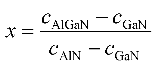 | (1) |
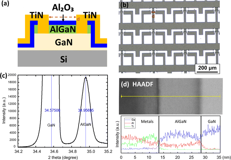 | ||
| Fig. 1 The structure and characterization of the AlGaN/GaN HEMTs. (a) Schematic diagram of the AlGaN/GaN HEMT with a TiN contact. (b) Plane view of the TLM pattern in our experiments. The channel lengths, d, of each contact pair are between 3–30 μm. (c) The XRD omega–2theta scan of a HEMT. (d) STEM HAADF image along with the EDS line scan profiles of the AlxGa1−xN/GaN substructure of the HEMT. | ||
Fig. 2 shows the current–voltage (I–V) characteristics of the AlGaN/GaN HEMTs with TiN as the contact metal after various annealing temperature treatments at as high as 1050 °C. The devices exhibited ohmic contact characteristics because the work function of TiN was close to GaN electron affinity.14,15 The ohmic characteristic retained after high temperature treatments between 700 and 1050 °C, which were typical processing temperatures required for GaN device. The consistent ohmic characteristics in the range of the temperatures displayed the good thermal stability of TiN on AlGaN/GaN HEMTs. The contacts still remained ohmic even after 1050 °C annealing where the lowest contact resistivity was about 8 × 10⁻⁵ Ω cm2 after 900 °C RTA. Even though the contact resistance was not as low as that in other reported cases (e.g. 2 to 5 × 10⁻⁶ Ω cm2 for Ti/Al), the TiN contacts were highly compatible to Si technology and highly stable during high temperature processing for GaN-related devices.
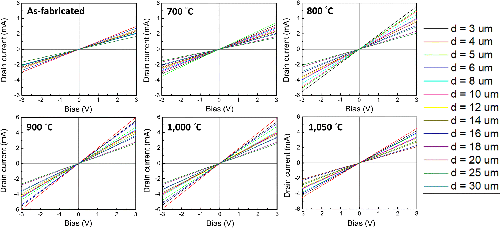 | ||
| Fig. 2 I–V characteristics of AlGaN/GaN HEMTs using TiN as the contact metal, including measurements from as-fabricated devices and those after high temperature annealing treatments between 700 and 1050 °C. | ||
In conventional cases, Au-containing Ti-based metal contacts were used to form ohmic contacts for GaN-based devices. During annealing, Ti in the metal contact and nitrogen in GaN form a thin TiN layer at the contact interface. It caused the generation of high-concentration N vacancies at the interface, and thus the contact resistance was reduced.16 However, these contact metals could not sustain high temperatures since annealing caused out-diffusion of Ti, followed by the formation of oxides.17 Au capping was applied to avoid such issues, while Au was unfavorable in CMOS technologies because it acted as deep-level traps in Si18 and was very mobile at low temperature (say 500 °C). For the unavoidable high processing temperature for GaN technology, TiN therefore provided an alternative choice to form a highly stable and reliable ohmic contact on GaN with reasonable contact resistance in a wide range of temperatures up to 1050 °C.
To make a comparison with a standard layout using Ti/Au as the contact material, we investigated the electrical properties and the interface microstructure of the devices with TiN and Ti/Au contacts as shown in Fig. 3. Fig. 3a and b present the I–V characteristics of devices after 1050 °C annealing where both of them exhibited ohmic contact characteristics. Fig. 3c and d reveal the large field of view of the morphology of the devices in an optical microscope. The illumination of the Ti/Au metal contacts and pads, shown in Fig. 3d, became darker after annealing with a small portion of the area remaining gold in color. This might indicate that most parts of Ti/Au diffused away and/or the surface became rougher. In contrast, the illumination form of TiN contacts after annealing looked similar (Fig. 3c) to its as-fabricated form. This demonstrated that the GaN device with TiN contacts behaved stably at high temperatures even at 1050 °C. From the cross-sectional STEM-BF images of the two devices with TiN and Ti/Au contacts on the GaN substrate (Fig. 3e and f), the TiN layer was stable and its thickness had no visible change after 1050 °C annealing, while the Au layer disappeared from the Ti/Au contact and only a thin layer of Ti or TiN, which might be produced by the reaction of Ti and GaN, was left at the interface. Therefore, after high temperature treatment, the total resistance from devices with Ti/Au was relatively high. While the annealing temperature reached of the RTA system is limited at 1050 °C, we suspect that the TiN contacts will be stable above 1050 °C because there was no visible thickness reduction or diffusion of the TiN contact at 1050 °C, and the melting point of TiN is higher than 2000 °C.
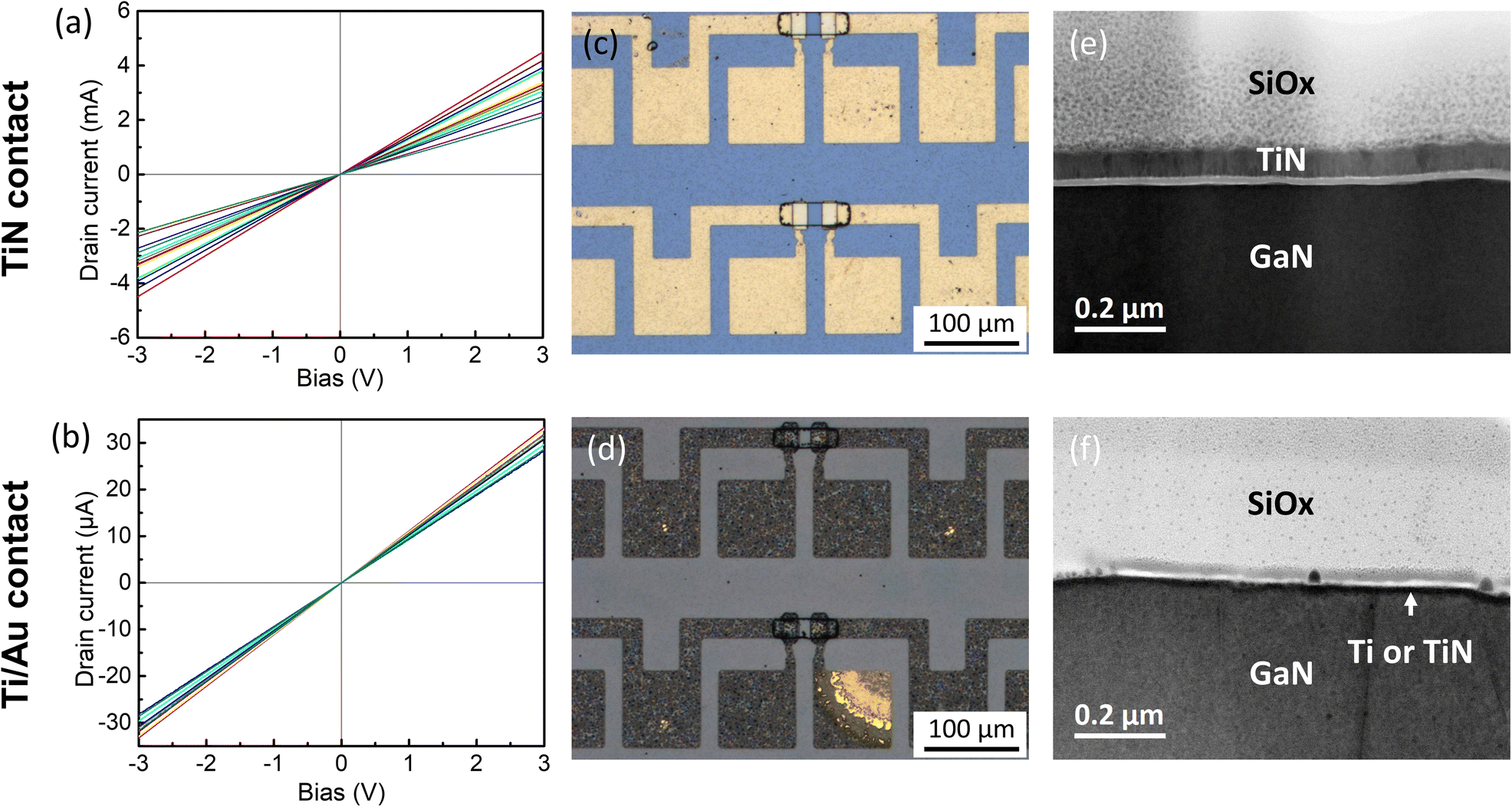 | ||
| Fig. 3 Thermal stability of TiN and Ti/Au contacts by comparison of the contact resistivity of TiN and Ti/Au on AlGaN/GaN HEMTs. I–V characteristics of (a) TiN (b) Ti/Au contacts on AlGaN/GaN HEMTs after 1050 °C annealing and the top-view morphology of (c) TiN and (d) Ti/Au contacts. The Ti/Au contact metal surface became rough after 1050 °C annealing. (e) and (f) show the cross-section TEM images of TiN and Ti/Au after 1050 °C annealing. Au diffused away from the Ti/Au contact due to the high annealing temperature. Note that the SiOX layer was deposited as a protection layer during TEM sample preparation. | ||
Fig. 4a shows the relationship between the total resistance and channel length of the AlGaN/GaN HEMTs with TiN contacts. The slope and vertical intercepts of fitting lines indicated the sheet resistance and the contact resistance. We found that the TiN contacts after 900 °C annealing had the lowest contact resistance. Fig. 4b shows the contact resistivity of the TiN and Ti/Au contacts on AlGaN/GaN HEMTs after annealing at different temperatures. In our case, the Ti/Au contacts were not ohmic when annealed below 1000 °C (ESI Fig. S1†). The contact resistivity with TiN was much lower than that with Ti/Au when annealing temperatures were higher than 1000 °C, which was consistent with the STEM images shown in Fig. 3e and f.
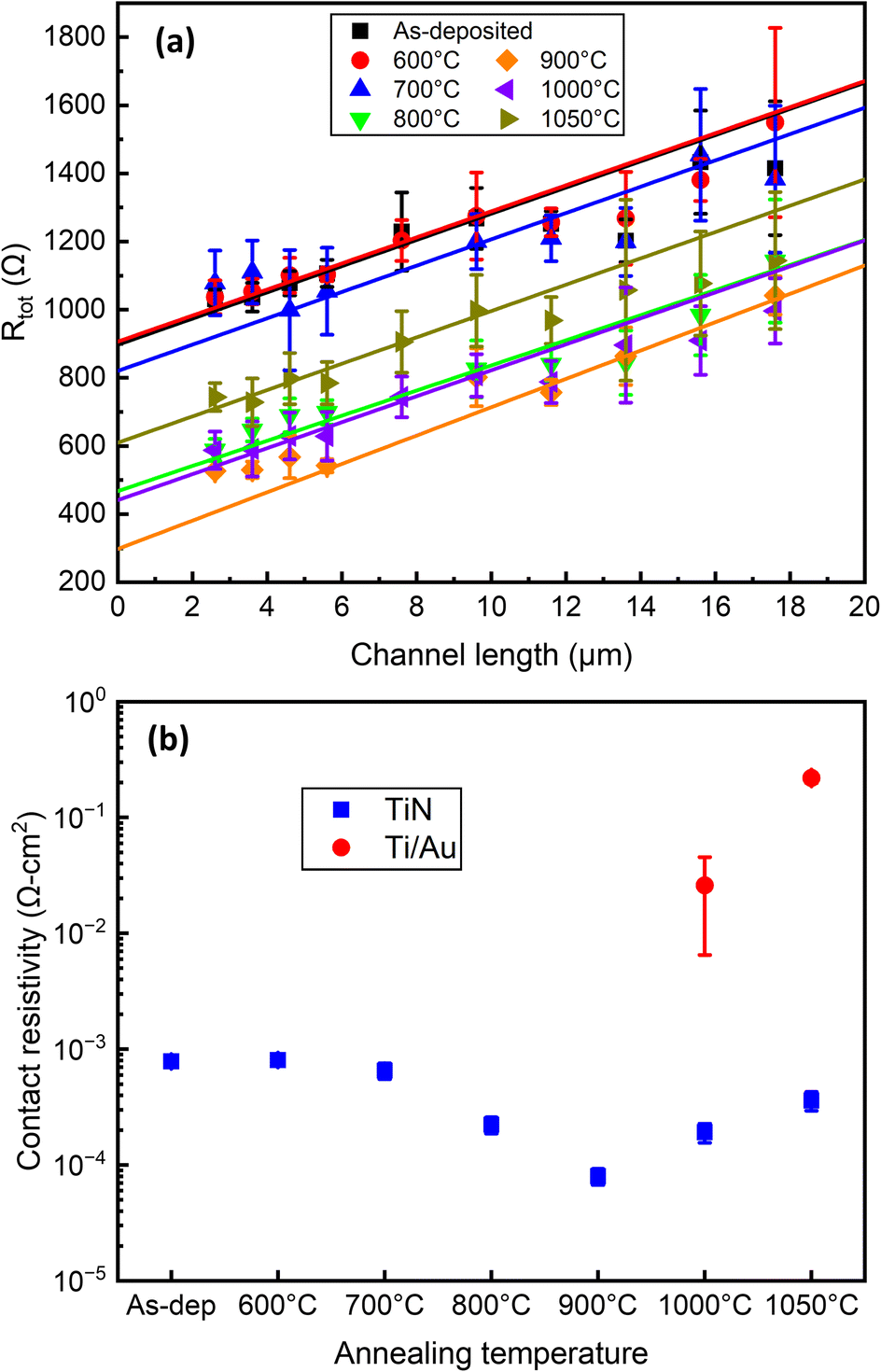 | ||
| Fig. 4 The contact resistivity of TiN and Ti/Au contacts on AlGaN/GaN HEMTs. (a) The total resistance of TiN contacts versus channel length. The vertical intercepts correspond to 2RC. (b) The contact resistivity of TiN and Ti/Au contacts on AlGaN/GaN HEMTs after the high temperature annealing. | ||
Besides, the TiN contacts presented better uniformity after high temperature treatments which could be attributed to its superior stability. Table 1 shows the comparison of the contact resistivity of TiN contacts on GaN-based devices reported in other papers and our work. Our result showed the same order of resistance even after processing at higher temperatures.
Compared to research on another contact metals for GaN devices,11,19,20 the resistivity of a TiN contact was a little higher. The higher resistance would cause the decay of device performance. Thus, to reduce the total resistance for the GaN device with a TiN contact metal, increasing TiN thickness or combining it with other refractory metal stacks might be the solutions. Even so, the TiN contact has high potential because it is highly compatible to Si technology and highly stable during high temperature processing for GaN-related devices.
To explore the chemistry of the contact interfaces, we furtherly carried out STEM EELS to characterize the TiN/GaN and TiN/AlGaN interface after 1050 °C annealing. Fig. 5a and b show the energy loss near edge structure (ELNES) of Ga-L3 and Al-K at the TiN/GaN and TiN/AlGaN interface. Compare to bulk GaN and AlGaN, the ELNES at the interface shows a positive chemical shift. This might be caused by the increase in the binding energy of Ga–N and Al–N bonds, which resulted in the decrease in Schottky barrier height, and therefore, the contacts were ohmic. For TiN grown by PEALD, the as-grown TiN/GaN showed an increase in the binding energy.12 In our results, the ELNES might also indicate an increase in the binding energy even when the annealing temperature was as high as 1050 °C. Fig. 5c shows the line profiles of the density of Ti and N atoms extracted from EELS at the interface. This illustrated that there was no Ti diffusion and the TiN layer stayed stable at 1050 °C.
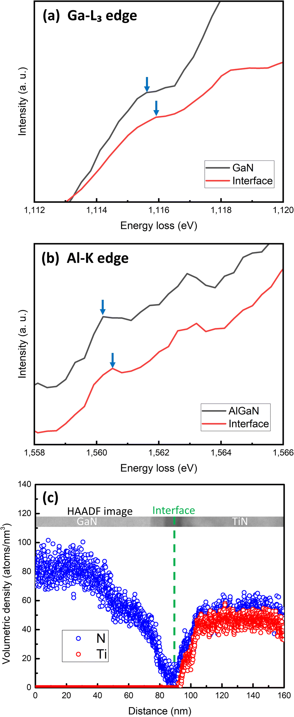 | ||
| Fig. 5 STEM EELS showing chemistry of the interfaces of TiN/GaN and TiN/AlGaN after heat treatment at 1050 °C. ELNES of the (a) Ga-L3 edge and (b) Al-K edge. The blue arrows indicate the position of the edges. Both of them have a positive chemical shift at the interface. (c) The line profiles of the density of Ti and N atoms extracted from EELS at the interface. | ||
Conclusions
In conclusion, a high-thermal stability ohmic contact metal, TiN, for high-processing temperature AlGaN/GaN HEMTs and related devices was reported. The lowest measured contact resistivity of TiN with GaN-based devices was 8 × 10⁻⁵ Ω cm2 after 900 °C annealing. Even though it was higher than that of other conventional devices, it provided excellent thermal stability at a series of high processing temperatures for GaN and compatibility with current Si technologies. The top-view morphology and cross-sectional STEM images showed that the TiN contacts were much more stable than the conventional Ti/Au contacts especially at temperatures higher than 1000 °C. In addition, it prevented Au contamination. The interface chemistry was analyzed using STEM EELS which showed the enhancement of the binding energy of Ga–N and Al–N and invisible diffusion of Ti during treatment below 1000 °C. This clarifies the origin of the highly stable ohmic contact. Thus, our studies on TiN contact material provide a new pathway and thought for forming reliable and thermally stable contacts for HEMTs or another GaN-based devices.Author contributions
C. Y. W. performed the sample preparation, STEM characterization, electrical measurements, and data analysis. T. S. C. participated in the analysis of the electrical properties. Y. C. C. supervised the project and the discussion of the data. All authors participated in the writing of the paper.Conflicts of interest
There are no conflicts to declare.Acknowledgements
Y. C. C. acknowledges support from the National Science and Technology Council of Taiwan under Grant No. 112-2112-M-002-047 and 112-2811-M-002-019. The authors gratefully thank Dr Ko-Tao Lee at Qorvo IDP Research for helpful discussion and acknowledge the core facility support from the National Science and Technology Council of Taiwan.References
- U. K. Mishra, L. Shen, T. E. Kazior and Y. F. Wu, Proc. IEEE, 2008, 96, 287–305 CAS.
- H. Amano, Y. Baines, E. Beam, M. Borga, T. Bouchet, P. R. Chalker, M. Charles, K. J. Chen, N. Chowdhury, R. Chu, C. De Santi, M. M. De Souza, S. Decoutere, L. Di Cioccio, B. Eckardt, T. Egawa, P. Fay, J. J. Freedsman, L. Guido, O. Häberlen, G. Haynes, T. Heckel, D. Hemakumara, P. Houston, J. Hu, M. Hua, Q. Huang, A. Huang, S. Jiang, H. Kawai, D. Kinzer, M. Kuball, A. Kumar, K. B. Lee, X. Li, D. Marcon, M. März, R. McCarthy, G. Meneghesso, M. Meneghini, E. Morvan, A. Nakajima, E. M. S. Narayanan, S. Oliver, T. Palacios, D. Piedra, M. Plissonnier, R. Reddy, M. Sun, I. Thayne, A. Torres, N. Trivellin, V. Unni, M. J. Uren, M. Van Hove, D. J. Wallis, J. Wang, J. Xie, S. Yagi, S. Yang, C. Youtsey, R. Yu, E. Zanoni, S. Zeltner and Y. Zhang, J. Phys. D: Appl. Phys., 2018, 51, 163001 CrossRef.
- K. J. Chen, O. Häberlen, A. Lidow, C. l. Tsai, T. Ueda, Y. Uemoto and Y. Wu, IEEE Trans. Electron Devices, 2017, 64, 779–795 CAS.
- H. S. Lee, K. Ryu, M. Sun and T. Palacios, IEEE Electron Device Lett., 2012, 33, 200–202 CAS.
- T. Matsumae, M. Fengwen, S. Fukumoto, M. Hayase, Y. Kurashima, E. Higurashi, H. Takagi and T. Suga, J. Alloys Compd., 2021, 852, 156933 CrossRef CAS.
- S. Fukumoto, T. Matsumae, Y. Kurashima, H. Takagi, H. Umezawa, M. Hayase and E. Higurashi, in 2021 7th International Workshop on Low Temperature Bonding for 3D Integration (LTB-3D), 2021, p. 11 Search PubMed.
- K. T. Lee, C. Bayram, D. Piedra, E. Sprogis, H. Deligianni, B. Krishnan, G. Papasouliotis, A. Paranjpe, E. Aklimi, K. Shepard, T. Palacios and D. Sadana, IEEE Electron Device Lett., 2017, 38, 1094–1096 CAS.
- G. Greco, F. Iucolano and F. Roccaforte, Appl. Surf. Sci., 2016, 383, 324–345 CrossRef CAS.
- H. Takeuchi, A. Wung, S. Xin, R. T. Howe and K. Tsu-Jae, IEEE Trans. Electron Devices, 2005, 52, 2081–2086 CrossRef.
- Y. Zhu, F. Li, R. Huang, T. Liu, Y. Zhao, Y. Shen, J. Zhang, A. Dingsun and Y. Guo, J. Vac. Sci. Technol., A, 2018, 36, 041501 CrossRef.
- J. Zhang, X. Kang, X. Wang, S. Huang, C. Chen, K. Wei, Y. Zheng, Q. Zhou, W. Chen, B. Zhang and X. Liu, IEEE Electron Device Lett., 2018, 39, 847–850 CAS.
- Y. Zhu, R. Huang, Z. Li, H. Hao, Y. An, T. Liu, Y. Zhao, Y. Shen, Y. Guo, F. Li and S. Ding, Appl. Surf. Sci., 2019, 481, 1148–1153 CrossRef CAS.
- H. P. Lee, J. Perozek, L. D. Rosario and C. Bayram, Sci. Rep., 2016, 6, 37588 CrossRef CAS PubMed.
- S. Gautier, K. Ph, P. Patsalas, K. Th, S. Logothetidis, C. A. Dimitriadis and G. Nouet, Semicond. Sci. Technol., 2003, 18, 594 CrossRef CAS.
- L. L. Smith, R. F. Davis, R. J. Liu, M. J. Kim and R. W. Carpenter, J. Mater. Res., 1999, 14, 1032–1038 CrossRef CAS.
- A. Shriki, R. Winter, Y. Calahorra, Y. Kauffmann, G. Ankonina, M. Eizenberg and D. Ritter, J. Appl. Phys., 2017, 121, 065301 CrossRef.
- F. M. Mohammed, L. Wang, I. Adesida and E. Piner, J. Appl. Phys., 2006, 100, 023708 CrossRef.
- W. M. Bullis, Solid-State Electron., 1966, 9, 143–168 CrossRef CAS.
- T. Yoshida and T. Egawa, Phys. Status Solidi A, 2018, 215, 1700825 CrossRef.
- B. Jacobs, M. C. J. C. M. Kramer, E. J. Geluk and F. Karouta, J. Cryst. Growth, 2002, 241, 15–18 CrossRef CAS.
- C. Maus, T. Stauden, G. Ecke, K. Tonisch and J. Pezoldt, Semicond. Sci. Technol., 2012, 27, 115007 CrossRef.
- B. P. Luther, S. E. Mohney and T. N. Jackson, Semicond. Sci. Technol., 1998, 13, 1322 CrossRef CAS.
Footnote |
| † Electronic supplementary information (ESI) available. See DOI: https://doi.org/10.1039/d3na00491k |
| This journal is © The Royal Society of Chemistry 2023 |