
 Open Access Article
 This Open Access Article is licensed under a Creative Commons Attribution-Non Commercial 3.0 Unported Licence
Influence of Sn doping on the optoelectronic properties of ZnO nanoparticles
Nadim
Munna†
ab,
Rahim
Abdur†
 b,
Robiul
Islam
bc,
Muhammad Shahriar
Bashar
b,
Syed Farid Uddin
Farhad
d,
Md.
Kamruzzaman
a,
Shahin
Aziz
b,
Md. Aftab Ali
Shaikh
ef,
Mosharof
Hossain
b and
Mohammad Shah
Jamal
*b
b,
Robiul
Islam
bc,
Muhammad Shahriar
Bashar
b,
Syed Farid Uddin
Farhad
d,
Md.
Kamruzzaman
a,
Shahin
Aziz
b,
Md. Aftab Ali
Shaikh
ef,
Mosharof
Hossain
b and
Mohammad Shah
Jamal
*b
aDepartment of Applied Chemistry and Chemical Engineering, University of Dhaka, Dhaka-1000, Bangladesh
bInstitute of Fuel Research and Development (IFRD), Bangladesh Council of Scientific and Industrial Research (BCSIR), Dr. Qudrat-E-Khuda Road, Dhanmondi, Dhaka-1205, Bangladesh. E-mail: msjdubd@gmail.com
cDepartment of Applied Chemistry and Chemical Engineering, Noakhali Science and Technology University, Noakhali-3814, Bangladesh
dBCSIR Laboratories Dhaka, Bangladesh Council of Scientific and Industrial Research (BCSIR), Dr. Qudrat-E-Khuda Road, Dhanmondi, Dhaka-1205, Bangladesh
eBangladesh Council of Scientific and Industrial Research (BCSIR), Dr. Qudrat-E-Khuda Road, Dhanmondi, Dhaka-1205, Bangladesh
fDepartment of Chemistry, University of Dhaka, Dhaka-1000, Bangladesh
First published on 17th August 2023
Abstract
Zinc Oxide (ZnO) nanoparticles (NPs) obtained a lot of attention from researchers and industries because of their superior properties as an optoelectronic material. Doping, especially tin (Sn), can further fine-tune their optoelectronic properties. In this manuscript, we have reported the optoelectronic properties of Sn-doped ZnO NPs, which were synthesized by a simple chemical solution method. A wide range of dopant (Sn) concentrations were used in the ratios of 0, 1, 3, 5, 7, and 10 weight percent. The effects of dopant (Sn) concentration on the structural, morphological, elemental composition, and optical properties of ZnO NPs were investigated by using an X-ray diffractometer (XRD), Field Emission Scanning Electron Microscope (FESEM), X-ray photoelectron spectrometer (XPS) and UV-Vis-NIR respectively. XRD analysis revealed the shifting of diffraction patterns towards a higher angle along with decreasing intensity. The calculated crystallite size using the XRD varied from 40.12 nm to 28.15 nm with an increasing doping percentage. Sn doping notably influences the size of ZnO NPs, along with crystal quality, strain, and dislocation density. The X-ray photoelectron spectroscopy (XPS) study showed the presence of zinc (Zn), oxygen (O), and tin (Sn) with their preferred oxidation states in the synthesized NPs. UV-Visible spectroscopy (UV-Vis) showed that the bandgap changed from 3.55 to 3.85 eV with the increasing concentration of Sn. FE-SEM revealed that the structures and surfaces were irregular and not homogeneous. The above findings for ZnO nanostructures show their potential application in optoelectronic devices.
Introduction
As a member of the metal oxide family, ZnO has attained a lot of attention from the scientific community, because of its wide bandgap (>3 eV),1 wide range conductivity,2 higher exciton binding energy,3,4 lower resistivity,1,5 non-toxicity, higher transparency within the visible range, and higher light-trapping properties.1,3,5 It has a hexagonal or wurtzite structure and the microstructure of ZnO has found numerous fundamental applications. Among them, the main application of ZnO at present is in photovoltaic applications,6–8 UV photo-detectors,9 thin-film transistors,10 photocatalysts of higher chemical activity, gas sensors,11 and varistors.12 ZnO semiconductors' electrical, optoelectronic, and piezoelectric properties can be tuned by various modification techniques. Along with these, different ZnO morphologies such as nanorods, nanotubes, nanoflowers, and nanowires offer exceptional opportunities to expand the range of applications. The development of UV lasers using ZnO nanorods has substantially accelerated research on ZnO nanorods and nanowires.13 In this regard, the controlled morphology, growth factors, and physical attributes of such structures are now very popular with researchers. Sol–gel, direct precipitation, hydrothermal and microwave-assisted thermal oxidation, and other chemical and physical techniques have been reported to synthesize ZnO nanoparticles.14,15 Most of the synthesis processes used hazardous chemicals, were expensive, required high temperatures, and took a long time to complete, all of which were shortcomings for industrial production.16 Several factors affect the properties of ZnO NPs, such as the pH of the reaction mixture, reaction temperature, zinc salt precursors, reaction time, concentration of precursors, precipitating agents, calcination temperature, etc.17The chemical solution process is one of the popular methods of synthesizing ZnO NPs, as in it, a simple precipitation method is used and requires simple chemicals.17–21 In this process, the size, shapes, and purity are easily controllable by tuning fewer parameters. Mostly zinc salt precursors, the pH of the reaction mixture, and calcination temperature play a vital role in the properties of ZnO NPs. Mayekar et al.22 reported that a zinc acetate precursor produces 39.91 nm spherical-shaped NPs with the highest purity compared to nitrate and chloride. In the case of the pH effect, lower pH values of the mixture produce larger crystals than higher pH values.17 The calcination process helps to fuse and grow larger than its initial crystallite size.23 Parra and Haque reported24 that the size of ZnO NPs increases from 30 nm to 44 nm with the calcination temperature increasing from 200 °C to 500 °C.
Nevertheless, the properties of synthesized NPs require further fine-tuning depending on their applications. Considering the optoelectronic application of ZnO NPs, the optical band gap, energy band gap band alignment, electrical conductivity, and surface morphology needed to be fine-tuned based on the other material's properties of that device as well as its architecture. Doping with different elements influences the crystallite size as well as other physical, optical, and chemical properties. Appropriate dopant choosing is an important issue in tuning desired properties. For ZnO doping, Sn has become a suitable candidate because it is considered an n-type dopant for the doping of ZnO nanoparticles. The radius of Sn4+ is 0.071 nm which is similar to that of Zn2+ (0.074 nm) and this helps in the effective replacement of Zn ions.1,2,12 Sn-doped ZnO can be effectively synthesized and its physical and chemical properties have been examined by several groups.18,19,25–28 Still, a systematic study can enrich this vast topic and facilitate future improvements and fine-tuning.
In this study, we have synthesized ZnO and Sn-doped ZnO NPs using a simple chemical solution process. To ensure spherical-shaped NPs with the highest purity, we have used zinc acetate as the Zn precursor, stannic chloride as the Sn precursor, and NaOH as the precipitating agent. Also to ensure uniform interaction conditions among the precursors and understand only the doping effect we have mixed precursors at a fixed rate with a slow stirring rate of 400 rpm. The Sn-dopant concentrations were varied in the ratios of 0, 1, 3, 5, 7, and 10 weight (wt%) percent of ZnO solution. The synthesized NPs were investigated systematically to understand the Sn-doping effect on ZnO using different physical, chemical, optical, and electrical characterization methods. Based on the properties of the ZnO NPs, the suitability of their application in optoelectronic devices, especially in photovoltaic devices, is discussed.
Materials and methods
Materials
All solvents and chemicals were purchased and utilized without further purification. Zinc acetate dihydrate [Zn(CH3COO)2·2H2O] (≥98%), sodium hydroxide (NaOH) (≥98%), tin(IV) chloride pentahydrate (SnCl4·5H2O) (≥98%), and 2-propanol (IPA) (extra pure) were purchased from Sigma-Aldrich Co. Whatman qualitative filter paper (110 mm ∅ × 100 circles) was purchased from a local vendor.Synthesis of ZnO NPs
ZnO NPs with Sn doping were synthesized following a method known as the chemical solution method. 50 mM Zn(CH3COO)2·2H2O and SnCl4·5H2O were prepared by dissolving 1.1075 g and 1.753 g in 100 mL of deionized water (DI) respectively. A 100 mM NaOH solution was also prepared by dissolving 0.4 g in 250 mL of DI. To synthesize ZnO NPs, 24 drops per minute of NaOH were added into the (Zn(CH3COO)2·2H2O) precursor solution until complete precipitation and the whole process was carried out under continuous magnetic stirring at 400 rpm. A white precipitate (ppts) of Zn(OH)2 was formed. The ppts were filtered using Whatman qualitative filter paper and washed using DI until unreacted NaOH was removed. After that, the ppts were oven-dried at 60 °C for 24 h. Then the ppts were ground using a Pulverisette 23 (FRITSCH, Germany) at 50 Hz for 4 min with 10 balls (total 2.1 g). Finally, the ground NPs were calcined at 500 °C for 5 h to oxidize Zn(OH)2 to ZnO. After cooling to room temperature, the ZnO NPs were used for different characterization methods.In the case of Sn-doped ZnO NPs, 1, 3, 5, 7, and 10 wt% SnCl4·5H2O solution were added to (Zn(CH3COO)2·2H2O) solution and stirred at 400 rpm for 2 h to confirm the complete mixing. Then the same process as for the synthesis of only ZnO NPs was followed.
A 1.5 wt% dispersion solution of ZnO and Sn-doped ZnO NPs was made by dispersing 0.075 g of NPs in 5 mL of IPA using vigorous sonication (Digital ultrasonic cleaner, LABTRON) at 40 kHz for 30 min. Then the dispersion was allowed to stand for 5 min to cool down and spin-coated on pre-cleaned glass substrates at 3000 rpm for 30 s. Finally, the films were annealed on a hot plate for 10 min at 100 °C to remove the remaining solvent from the thin film.
Characterization
ZnO and Sn-doped ZnO NP powder crystallographic information was obtained using XRD (Cu Kα radiation, λ = 0.15406 nm, 40 kV and 60 mA, scanning range of 20–80°, and ARL Equinox 1000, Thermo Scientific™, USA), morphological information was achieved using Field Emission Scanning Electron Microscopy (FE-SEM) (JEOL-7610F, Japan), and elemental composition was observed by Energy Dispersive Spectroscopy (EDS) coupled with FE-SEM (JEOL-7610F, Japan) and Scanning Electron Microscopy (SEM) (Carl Zeiss AG, EV018, UK). ZnO and Sn-doped ZnO NP thin films prepared on a glass substrate were used to characterize compositional information with the chemical state using X-ray photoelectron spectroscopy (XPS, K-alpha, Thermo Scientific™, USA), and optical transmission with an optical bandgap was characterized using UV-Visible spectroscopy (UH4150 Spectrophotometer (Integrating Sphere), Hitachi, Japan) from 280 nm to 800 nm at a 600 nm per minute scanning rate. Electrical properties were acquired using a Hall measurement equipment (Ecopia Corp., HMD-3000, South Korea). Inductively Coupled Plasma Mass Spectroscopy (ICP-MS) (PerkinElmer, Model: NexION 2000) was used to further analyze Zn and Sn contents in the prepared NPs.Results and discussion
Structural properties
The XRD patterns of the NP powders are shown in Fig. 1. Sharp diffraction peaks (2θ) are located at 31.84°, 34.52°, 36.28°, 47.5°, 56.65°, 62.87°, 68.00°, 69.13°, 72.62°, 77.06°, and 81.47° attributed respectively to the (100), (002), (101), (102), (110), (103), (200), (112), (201), and (004) crystal planes of the hexagonal close-packed (HCP) ZnO structure (JCPDS card no. 01-1136).29 No other diffraction patterns related to SnO2 or any other impurities were not observed even at 10% doping concentration.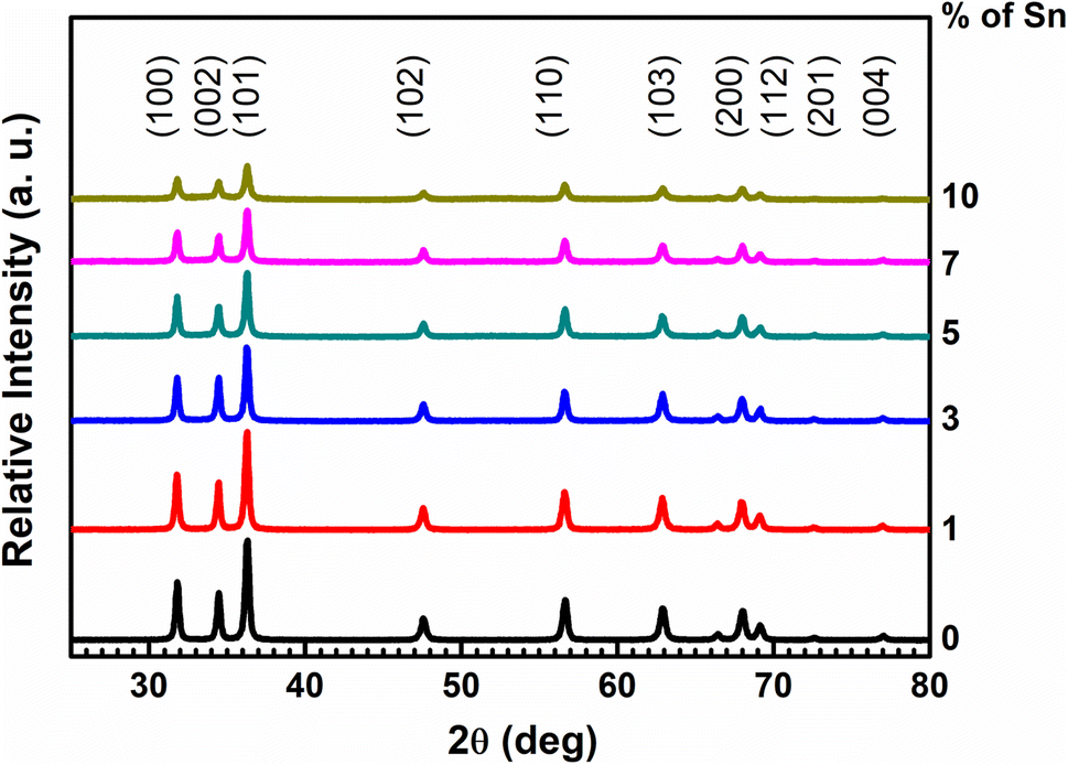 | ||
| Fig. 1 Variation of the XRD pattern of ZnO NPs with the Sn doping percentage. | ||
With the increase in the Sn doping percentage, all the reflections' intensity decreased. This effect is mainly due to the difference in ionic radii between the Zn and the dopant Sn.30 The smaller ionic radii Sn4+ (0.69 Å), substitutes Zn2+ (0.69 Å) or insert into the vacant Zn2+ sites in the ZnO lattice. This smaller-sized Sn4+ makes stronger interaction with O2− in the lattice,12,31 which induces strain in the lattice leading to FWHM broadening with intensity reduction of all the diffraction patterns. This substitution or insertion was not site-selective, so several diffraction patterns shifted with increasing doping percent. All the samples showed a preferred orientation towards the (101) diffraction plane. The reflection position shifting of the (101) plane, full width at half maxima (FWHM) values of the (101) plane, crystallite size, microstrain, and dislocation density variation with the doping percentage are listed in Table 1.
| Doping percentage (%) | Peak position (degree) | FWHM (degree) | Crystallite size (nm) | Microstrain × 10−3 (%) | dislocation density (m−2) |
|---|---|---|---|---|---|
| 0 | 36.21 | 0.23 | 40.73 | 3.04 | 0.60 |
| 1 | 36.24 | 0.24 | 38.38 | 3.23 | 0.68 |
| 3 | 36.29 | 0.26 | 36.43 | 3.40 | 0.75 |
| 5 | 36.35 | 0.28 | 33.06 | 3.73 | 0.91 |
| 7 | 36.41 | 0.28 | 32.60 | 3.78 | 0.94 |
| 10 | 36.47 | 0.33 | 28.08 | 4.38 | 1.27 |
Table 1 column 2 shows the continuous shifting of the (101) plane towards a higher angle with the increase of the Sn doping percentage to ZnO, indicating that Sn4+ can replace Zn2+ ions without altering the crystal structure.30 The crystallite size of the un-doped and Sn-doped ZnO NPs was calculated from the XRD data using Debye–Scherrer's formula.32 The equation is:
 | (1) |
Morphology study
The FE-SEM morphological images of pure ZnO and Sn-doped ZnO NPs are shown in Fig. 2. The images vividly depict the morphological changes caused by various amounts of Sn doping in ZnO. The nature is inhomogeneous when it comes to Sn-doped ZnO NPs.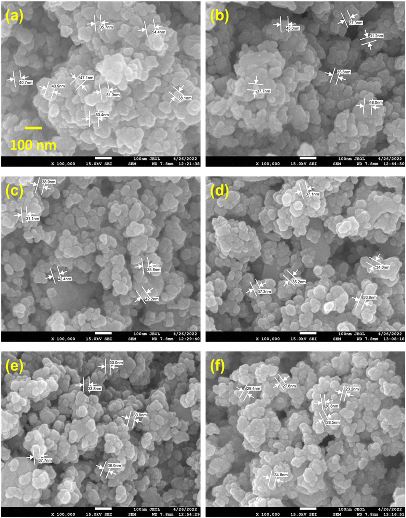 | ||
| Fig. 2 FE-SEM morphological image of the synthesized Sn-doped ZnO NPs with (a) 0, (b) 1, (c) 3, (d) 5, (e) 7, and (f) 10 wt% doping percent. | ||
Microstructural deviations demonstrate the method of nucleation development when the doping rate is increased.12 Sn atoms cause these fluctuations by promoting rapid nucleation leading to the reduction of the particle size, by which the microstructure is relaxed and lowers the energy of the system. Additionally, the surface revealed that Sn doping has a significant impact. Sn mainly modifies and enhances the ZnO NP structure.12 The most important component in determining the final product's shape and structure was the Sn ratio. Several microstructure sizes were measured to predict the average microstructure size of the synthesized NPs. The microstructure size was 45.58 ± 7.11, 39.13 ± 6.22, 38.08 ± 4.75, 35.44 ± 1.71, 34.46 ± 3.04, and 27.38 ± 4.92 nm for 0, 1, 3, 5, 7, and 10 wt% Sn doping into ZnO NPs respectively. These data show a similar tendency to the XRD-derived crystallite size data.
Electrical properties
The electrical properties of the pure ZnO and Sn-doped ZnO thin films, fabricated from the synthesized NPs, were carried out using the van der Pauw method.33 All the films showed n-type semiconductor behavior. The bulk carrier concentration for the pure ZnO thin film was found to be 2.46 × 1011 cm−3 and increased with Sn doping concentration up to 3.03 × 1013 cm−3 for 10% Sn doping. Fig. 3(a) illustrates the carrier concentration variation with Sn doping concentration. As the Sn4+ ion substitutes the Zn2+ ion in the ZnO lattice or inserts in the vacant sites of the lattice, it creates extra free electrons increasing the bulk carrier concentration. In the case of mobility, trends decrease with increasing Sn doping concentration, as illustrated in Fig. 3(b). As doping increases the bulk density increase leading to a decrease in mobility. On the other hand, the resistivity of the thin films (Fig. 3(c)) decreased up to 9.60 × 10² Ω cm for 5% Sn doping from 1.46 × 10⁴ Ω cm for pure ZnO and then increased again for further doping.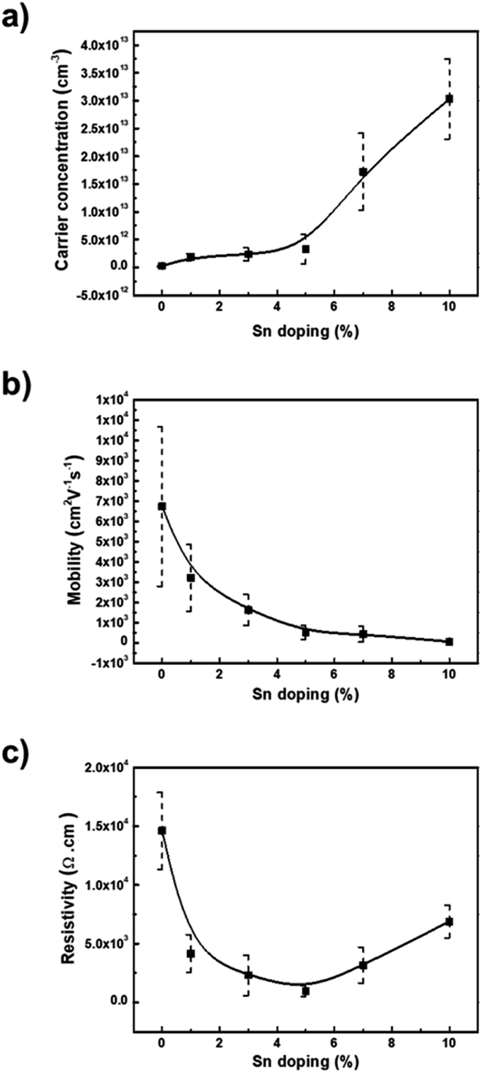 | ||
| Fig. 3 (a) Carrier concentration variation of the bulk ZnO NP thin films, (b) mobility of free carriers in the ZnO NP thin films, and (c) resistivity variation of the ZnO NP thin film with the Sn doping percent. | ||
Optical properties
The optical transmittance spectra for pure ZnO with Sn-doped nanostructured thin films are shown in Fig. 4(a) for wavelengths ranging from 300 to 800 nm. According to this graph, all the films were highly transparent in the visible range with a rapid reduction in the UV region, which is somewhat moved to lower wavelengths with the Sn doping percentage increasing. The mean optical transmittance throughout the visible region for pure ZnO thin films was about 87%, with an absorption edge at approximately 369 nm (Fig. 4(a)). Sn-doped ZnO NPs displayed better transparency than pure ZnO NPs, as shown in Fig. 4(a). Furthermore, the average transmittances of 1 wt% doped films were lower than those of pure films. This conclusion is consistent with surface roughness assessments. According to Lee et al.,34 the reduced transmittance in Sn-doped ZnO thin films could be due to increased optical scattering generated by their rough surface morphology. In this work, the 10 wt% Sn-doped ZnO thin film had the highest transparency amongst the doped samples, with 98.65 percent average transparency.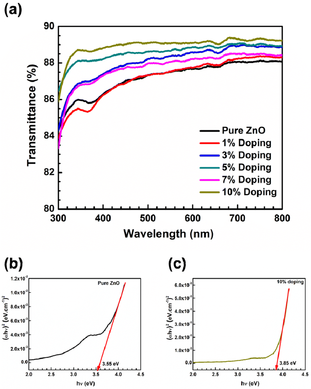 | ||
| Fig. 4 (a) Transmittance of the Sn-doped ZnO NP thin films fabricated on bare glass, and Tauc plot of (b) pure ZnO NPs, and (c) 10 wt% Sn-doped ZnO NPs used to calculate the optical bandgap. | ||
The optical band gap of pure ZnO (Fig. 4(b)) and Sn-doped ZnO (Fig. 4(c)) NP thin films is computed from the Tauc plot between hν (eV) and (αhν)2. The following well-known equation is used to compute the direct optical bandgap:
| (αhν)1/n = B(hν − Eg) | (2) |
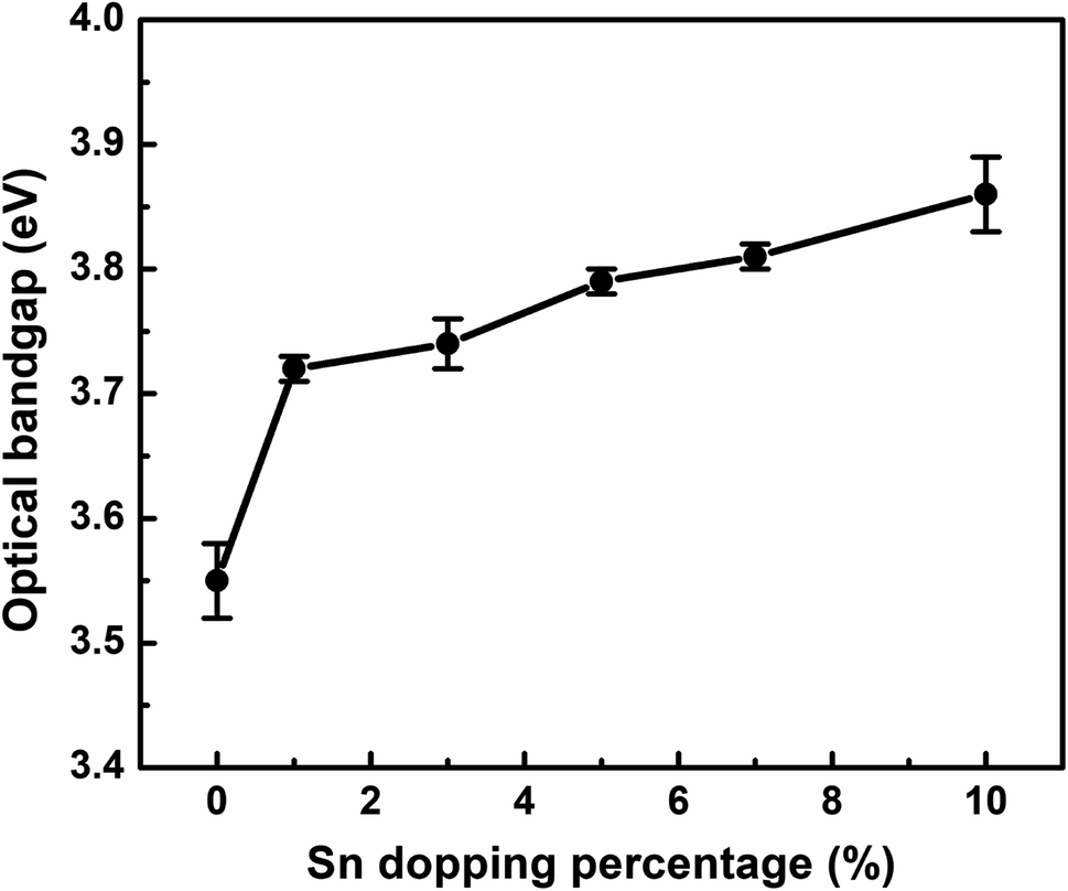 | ||
| Fig. 5 Optical bandgap variation of Sn-doped ZnO NPs with the Sn doping percentage. | ||
This optical band gap tuning of Sn-doped ZnO NPs enables the suitability of applying them in various optoelectronic devices37 including photovoltaics.
Compositional analysis
The EDS analysis of pure ZnO and Sn-doped ZnO NPs is illustrated in Fig. 6. Pure ZnO NPs showed only Zn and O elemental peaks (Fig. 6(a)). On the other hand, Sn-doped ZnO NPs showed Zn, Sn, and O elemental peaks (Fig. 6(b–f)). The Sn atomic percent increased with increasing Sn doping percent, though the atomic percent does not directly depict the original doping percent, but rather illustrates the doping increasing trend.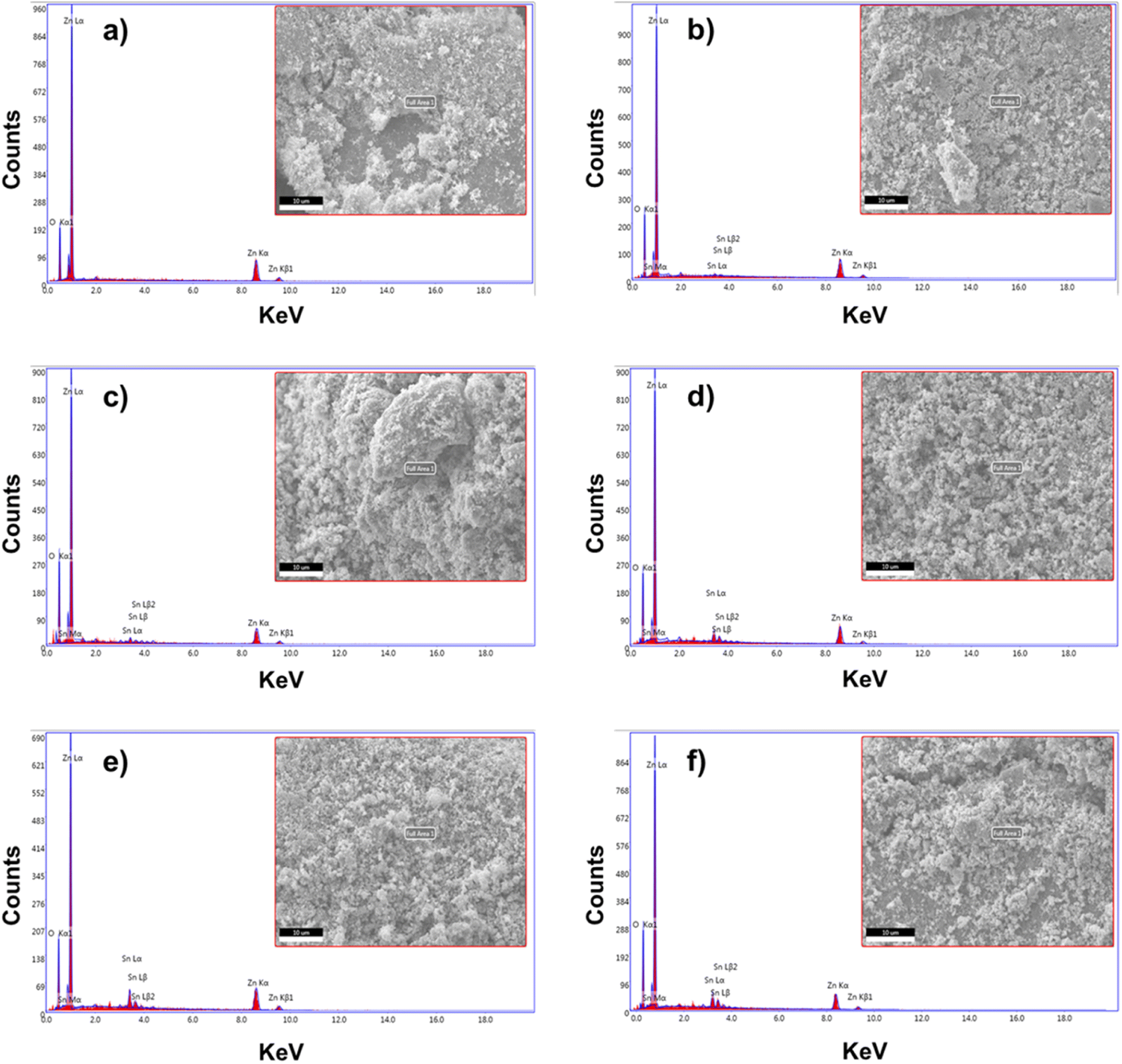 | ||
| Fig. 6 SEM morphological image with EDS mapping of the synthesized Sn-doped ZnO NPs with (a) 0, (b) 1, (c) 3, (d) 5, (e) 7, and (f) 10 wt% doping percent. | ||
To check the Sn atomic percent present in the ZnO NPs, the samples were further characterized with ICP-MS. The sample was digested with HCl. The processed acid digested samples were directly analyzed using an ICP-MS. The data from the ICP-MS were processed with Syngistix™ software for their heavy metal contents following the process reported by Roychowdhuri et al.38 The glassware utilized in this experiment underwent a thorough cleaning process, involving ultrapure acid and water, to minimize the potential for contamination during both sample preparation and analytical procedures. Prior to calibration with standards, the performance of the ICPMS equipment was assessed using a NexION Setup solution from PerkinElmer, USA. A calibration variance of five points was successfully achieved, with an R2 value > 0.9995. To ensure the stability of the instrument, a minimum of three replicates were performed. A maximum relative standard deviation (RSD) of 5–8% was taken into consideration. The detection (DL) and quantification (QL) limits of the instrument were established by determining the point at which the signal for a particular metal exceeded the background noise by three and ten times, respectively. The quality control process involved the execution of procedures, determination of SRM recoveries, and assessment of spike recoveries in order to mitigate potential errors. The concentrations of trace metals were adjusted based on recoveries and blank sample analysis. The average values with standard deviation are presented in Table 2.
| Sample | Atomic percentage (%) | ||||
|---|---|---|---|---|---|
| EDS | ICP-MS | ||||
| Zn | Sn | O | Zn | Sn | |
| Pure ZnO | 60.23 ± 5.30 | Not detected | 39.77 ± 5.30 | 79.66 ± 0.65 | Not detected |
| 1% Sn doped ZnO | 55.20 ± 2.76 | 0.45 ± 0.17 | 44.35 ± 2.82 | 79.12 ± 1.28 | 0.87 ± 0.04 |
| 3% Sn doped ZnO | 63.79 ± 25.47 | 1.01 ± 0.45 | 35.19 ± 25.04 | 77.84 ± 0.57 | 2.77 ± 0.14 |
| 5% Sn doped ZnO | 59.52 ± 14.71 | 3.04 ± 1.53 | 37.44 ± 13.18 | 76.69 ± 0.63 | 4.86 ± 0.32 |
| 7% Sn doped ZnO | 51.52 ± 6.65 | 4.60 ± 1.00 | 43.89 ± 6.98 | 74.54 ± 0.76 | 6.74 ± 0.14 |
| 10% Sn doped ZnO | 46.72 ± 2.91 | 5.96 ± 1.64 | 47.32 ± 1.75 | 71.90 ± 0.37 | 9.37 ± 0.47 |
The XPS spectra of 5 wt% Sn-doped ZnO NPs are shown in Fig. 7. The presence of zinc (Zn), oxygen (O), and tin (Sn) is indicated by the presence of obvious Zn 2p, O 1s, and Sn 3d peaks. The binding energies were measured using the C 1s peak as a benchmark (284.5 eV). All the data were deconvoluted using simulation software XPSPEAK41. Black lines represent raw data, dotted red lines represent simulated data, and other colored lines represent deconvoluted peaks to fit the simulated data in Fig. 7. The binding energies of the deconvoluted Zn 2p spectral peaks (Fig. 7(a)) are 1021.9 eV and 1044.8 eV, for Zn 2p3/2 and Zn 2p1/2, respectively, with the corresponding satellite peaks.
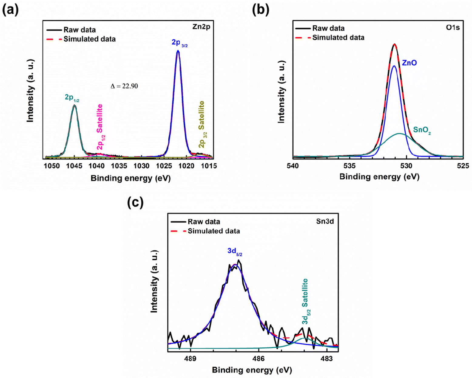 | ||
| Fig. 7 Deconvoluted XPS spectra of (a) Zn 2p, (b) O 1s, and (c) Sn 3d of 5 wt% Sn-doped ZnO NPs. | ||
which confirm the presence of ZnO.30 The deconvoluted O 1s spectrum (Fig. 7(b)) showed peaks at 531.1 and 530.6 eV, confirming the presence of ZnO and SnO2 respectively.30 Finally, the spectral peak of Sn 3d (Fig. 7(c)) is deconvoluted into two peaks. The peaks at 487.08 and 483.98 eV represent Sn 3d5/2 and its satellite peak respectively for SnO2.30 These results confirm the successful Sn doping of ZnO.
Conclusions
Tin (Sn) doped zinc oxide (ZnO) NPs were synthesized by a simple chemical solution process. It was found that doping of Sn significantly altered the morphology of ZnO NPs, confirmed by FE-SEM. Sn doping has a notable influence on the size of ZnO NPs, as well as the crystal quality, microstrain, and dislocation density of ZnO nanoparticles, according to data analyzed by XRD. An XPS study showed the presence of Zn, O, and Sn elements in the 5 wt% Sn-doped ZnO NPs. Also, the binding energy of these elements confirmed the Zn2+ substitution by Sn4+ in the Sn-doped ZnO NPs. UV-Visible spectroscopy revealed that the band gap increases with the increasing concentration of Sn. Meanwhile the electrical properties revealed the lowest resistivity of 9.60 × 10² Ω cm for the 5% Sn-doped ZnO NP thin film with an optical band gap of 3.79 eV. These wide band gap Sn-doped ZnO NPs can be suitable for optoelectronic applications such as photovoltaic devices.Author contributions
N. M.: data curation, formal analysis, investigation, validation, and writing-original draft. R. A.: data curation, formal analysis, investigation, methodology, visualization, validation, supervision, and writing-review & editing. R. I.: data curation and validation. S. F. U. F.: investigation and validation. M. K.: writing-review & editing. S. A.: writing-review & editing. M. A. S. A.: writing-review & editing. M. H.: supervision, writing-review & editing, and funding acquisition. M. S. J.: conceptualization, funding acquisition, project administration, validation, supervision, and writing – review & editing.Conflicts of interest
The authors declare that they have no conflict of interest.Acknowledgements
This work was carried out under the R&D project (FY 2021-2022) of IFRD, BCSIR titled “Synthesis of Graphene Nanorod as Electron Transport Layer (ETL) for Perovskite Solar Cells (PSCs)”.References
- S. Ameen, M. S. Akhtar, H. K. Seo, Y. S. Kim and H. S. Shin, Chem. Eng. J., 2012, 187, 351–356 CrossRef CAS.
- C. Y. Tsay, H. C. Cheng, Y. T. Tung, W. H. Tuan and C. K. Lin, Thin Solid Films, 2008, 517, 1032–1036 CrossRef CAS.
- S. Fiedler, L. O. L. C. Lem, C. Ton-That, M. Schleuning, A. Hoffmann and M. R. Phillips, Sci. Rep., 2020, 10, 1–9 CrossRef PubMed.
- D. G. Thomas, J. Phys. Chem. Solids, 1960, 15, 86–96 CrossRef CAS.
- Y. Caglar, S. Aksoy, S. Ilican and M. Caglar, Superlattices Microstruct., 2009, 46, 469–475 CrossRef CAS.
- L. Lin and N. M. Ravindra, Emerging Mater. Res., 2020, 9, 812–824 CrossRef.
- I. Repins, M. A. Contreras, B. Egaas, C. DeHart, J. Scharf, C. L. Perkins, B. To and R. Noufi, Prog. Photovoltaics, 2008, 16, 235–239 CAS.
- J. Ramanujam, D. M. Bishop, T. K. Todorov, O. Gunawan, J. Rath, R. Nekovei, E. Artegiani and A. Romeo, Prog. Mater. Sci., 2020, 110, 100619 CrossRef CAS.
- M. R. Hasan, T. Xie, S. C. Barron, G. Liu, N. V. Nguyen, A. Motayed, M. V. Rao and R. Debnath, APL Mater., 2015, 3, 106101 CrossRef PubMed.
- S. Lee, Y. Jeong, S. Jeong, J. Lee, M. Jeon and J. Moon, Superlattices Microstruct., 2008, 44, 761–769 CrossRef CAS.
- S. Kumar, V. Singh and A. Tanwar, J. Mater. Sci.: Mater. Electron., 2016, 27, 2166–2173 CrossRef CAS.
- M. Arshad Javid, M. Rafi, I. Ali, F. Hussain, M. Imran and A. Nasir, Mater. Sci. Polym., 2016, 34, 741–746 CrossRef.
- R. Zhang, P.-G. Yin, N. Wang and L. Guo, Solid State Sci., 2009, 11, 865–869 CrossRef CAS.
- S. Musić and A. Šarić, Ceram. Int., 2012, 38, 6047–6052 CrossRef.
- S.-H. Yu, J. Yang, Y.-T. Qian and M. Yoshimura, Chem. Phys. Lett., 2002, 361, 362–366 CrossRef CAS.
- K. Handore, S. Bhavsar, A. Horne, P. Chhattise, K. Mohite, J. Ambekar, N. Pande and V. Chabukswar, J. Macromol. Sci., Part A: Pure Appl.Chem., 2014, 51, 941–947 CrossRef CAS.
- E. Y. Shaba, J. O. Jacob, J. O. Tijani and M. A. T. Suleiman, Appl. Water Sci., 2021, 11, 48 CrossRef CAS.
- M. Kahouli, A. Barhoumi, A. Bouzid, A. Al-Hajry and S. Guermazi, Superlattices Microstruct., 2015, 85, 7–23 CrossRef CAS.
- M. K. Debanath and S. Karmakar, Mater. Lett., 2013, 111, 116–119 CrossRef CAS.
- H. Ghorbani, F. Mehr, H. Pazoki and B. Rahmani, Orient. J. Chem., 2015, 31, 1219–1221 CrossRef CAS.
- G. Taka and T. D. Das, IOP Conf. Ser.: Earth Environ. Sci., 2022, 1042, 012017 CrossRef.
- S. Mayekar, J. Dhar and V. Radha, et al. , Int. J. Res. Eng. Technol., 2014, 03, 43–45 Search PubMed.
- A. Ruys, in Alumina Ceramics, Elsevier, 2019, pp. 473–499 Search PubMed.
- M. R. Parra and F. Z. Haque, J. Mater. Res. Technol., 2014, 3, 363–369 CrossRef CAS.
- E. K. Droepenu, Biointerface Res. Appl. Chem., 2022, 12, 4261–4292 CAS.
- P. M. Aneesh, K. A. Vanaja and M. K. Jayaraj, in Nanophotonic Materials IV, eds., Z. Gaburro and S. Cabrini, SPIE, 2007, vol. 6639, p. 66390J Search PubMed.
- S. Arya, P. Mahajan, S. Mahajan, A. Khosla, R. Datt, V. Gupta, S.-J. Young and S. K. Oruganti, ECS J. Solid State Sci. Technol., 2021, 10, 023002 CrossRef CAS.
- H. Mirzaei and M. Darroudi, Ceram. Int., 2017, 43, 907–914 CrossRef CAS.
- J. D. Hanawalt, H. W. Rinn and L. K. Frevel, Ind. Eng. Chem. Anal. Ed., 1938, 10, 457–512 CrossRef CAS.
- M. Jung, S. Kim and S. Ju, Opt. Mater., 2011, 33, 280–283 CrossRef CAS.
- M. Verma, P. K. Dwivedi and B. Das, J. Exp. Nanosci., 2015, 10, 438–448 CrossRef CAS.
- T. Fukumura, Z. Jin, A. Ohtomo, H. Koinuma and M. Kawasaki, Appl. Phys. Lett., 1999, 75, 3366–3368 CrossRef CAS.
- F. S. Oliveira, R. B. Cipriano, F. T. da Silva, E. C. Romão and C. A. M. dos Santos, Sci. Rep., 2020, 10, 16379 CrossRef CAS PubMed.
- J.-H. Lee and B.-O. Park, Thin Solid Films, 2003, 426, 94–99 CrossRef CAS.
- T. S. Moss, Proc. Phys. Soc., London, Sect. B, 1954, 67, 775–782 CrossRef.
- W. K. Munguti, L. K. Musembi and R. J. Njoroge, et al. , Elixir Thin Film Technol., 2013, 61, 17162–17165 Search PubMed.
- K. Saravanakumar, P. Sakthivel and R. K. Sankaranarayanan, Spectrochim. Acta, Part A, 2022, 267, 120487 CrossRef CAS.
- T. Roychowdhury, T. Uchino, H. Tokunaga and M. Ando, Food Chem. Toxicol., 2002, 40, 1611–1621 CrossRef CAS PubMed.
Footnote |
| † Nadim Munna and Rahim Abdur contributed equally to this work. |
| This journal is © The Royal Society of Chemistry 2023 |