
 Open Access Article
 This Open Access Article is licensed under a
 Creative Commons Attribution 3.0 Unported Licence
ALD-grown two-dimensional TiSx metal contacts for MoS2 field-effect transistors†
Reyhaneh
Mahlouji
 *a,
Wilhelmus M. M. (Erwin)
Kessels
a,
Abhay A.
Sagade
*b and
Ageeth A.
Bol
*a
*a,
Wilhelmus M. M. (Erwin)
Kessels
a,
Abhay A.
Sagade
*b and
Ageeth A.
Bol
*a
aDepartment of Applied Physics, Eindhoven University of Technology, P. O. Box 513, 5600 MB, Eindhoven, The Netherlands. E-mail: r.mahlouji@tue.nl; a.a.bol@tue.nl
bDepartment of Physics and Nanotechnology, Laboratory for Advanced Nanoelectronic Devices, SRM Institute of Science and Technology, SRM Nagar, Kattankulathur, 603 203, Tamil Nadu, India. E-mail: abhaya@srmist.edu.in
First published on 15th August 2023
Abstract
Metal contacts to MoS2 field-effect transistors (FETs) play a determinant role in the device electrical characteristics and need to be chosen carefully. Because of the Schottky barrier (SB) and the Fermi level pinning (FLP) effects that occur at the contact/MoS2 interface, MoS2 FETs often suffer from high contact resistance (Rc). One way to overcome this issue is to replace the conventional 3D bulk metal contacts with 2D counterparts. Herein, we investigate 2D metallic TiSx (x ∼ 1.8) as top contacts for MoS2 FETs. We employ atomic layer deposition (ALD) for the synthesis of both the MoS2 channels as well as the TiSx contacts and assess the electrical performance of the fabricated devices. Various thicknesses of TiSx are grown on MoS2, and the resultant devices are electrically compared to the ones with the conventional Ti metal contacts. Our findings show that the replacement of 5 nm Ti bulk contacts with only ∼1.2 nm of 2D TiSx is beneficial in improving the overall device metrics. With such ultrathin TiSx contacts, the ON-state current (ION) triples and increases to ∼35 μA μm−1. Rc also reduces by a factor of four and reaches ∼5 MΩ μm. Such performance enhancements were observed despite the SB formed at the TiSx/MoS2 interface is believed to be higher than the SB formed at the Ti/MoS2 interface. These device metric improvements could therefore be mainly associated with an increased level of electrostatic doping in MoS2, as a result of using 2D TiSx for contacting the 2D MoS2. Our findings are also well supported by TCAD device simulations.
Introduction
Transition metal di-chalcogenides (TMDCs) are a family of two-dimensional (2D)-layered materials with a chemical formula of MX2 (M = Mo, W, Ti, Nb, V, etc. and X = S, Se, Te).1,2 2D TMDCs constitute a wide library of compounds ranging from semiconductors and (semi)metals to superconductors.3 Among semiconducting 2D TMDCs, MoS2 is the most widely explored material because of its abundance in nature and its outstanding electronic properties.4,5 Field-effect transistors (FETs) based on MoS2 demonstrate high current densities of 700–1135 μA μm−1,6–8 high ON/OFF current ratios in the range of 107–109,5,9,10 low subthreshold swing (SS) values close to the thermionic limit (∼60 mV dec−1),11,12 reasonably good mobility,5,13,14 decent reliability,9 relatively low variability15 and compatibility with conventional Si processing technologies.16–18 These fascinating features of MoS2 FETs may open new horizons for ultra-scaled nanoelectronic devices and circuits.19,20Implementation of MoS2 or any other 2D TMDC into mainstream technology platforms is not without hurdles. 2D FETs generally suffer from high contact resistance (Rc),21 which is still above the requirements specified by the International Roadmap for Devices and Systems (IRDS).22 High Rc originates from the unavoidable Schottky barrier (SB) formation and Fermi level pinning (FLP) effect at the metal–semiconductor (M–S) junctions.23,24 In recent years, several attempts have been made to tackle high Rc in 2D FETs, namely substitutional/chemical doping of the 2D layer,25,26 2D phase engineering at the contact regions,27 the insertion of oxide buffer layers (Ta2O3, Al2O3) below the contacts,28,29 electrostatically doping the 2D channel by high-κ dielectrics,6,10,30 switching to edge contact device geometry (rather than using the conventional top contact device geometry)31–34 and utilization of semi-metal,8 graphene32,35–38 or metallic 2D TDMC contacts.34,39,40 To date, the lowest Rc records are in the range of 123–520 Ω μm, being held for semi-metal8 or graphene contacts,37 phase engineering the 2D layer at the contact areas,27 dielectric mediated charge transfer doping of the 2D channel6 and metallic 2D TMDC employment in edge contact device geometry.34
Among the above-mentioned methods for reducing Rc, the usage of 2D metallic contacts, such as VS2,34 VSe2![[thin space (1/6-em)]](https://www.rsc.org/images/entities/char_2009.gif) 39 or NbS2,40 in 2D FETs has lately gained a surging interest. Conventional bulk metallic contacts are known to form covalent bonds with the 2D semiconducting layer,41 leading to charge redistribution at the M–S junction, work function (WF) modulations and metal-induced gap state (MIGS)42 formation as well as 2D electronic band-structure perturbation that altogether result in high SB/strong FLP14,41–43 and therefore an overall high Rc. 2D metallic contacts, on the other hand, offer several advantages over the 3D bulk counterparts. First and foremost, they only weakly bind/react with 2D semiconductors. This is mainly because of the overall weak van der Waals (vdW) interactions that leads to an almost clean and flat vdW interface at the 2D–2D M–S junctions, wherein lattice matching becomes less important.44 Such vdW interactions are also shown to suppress MIGS and allow for an almost unperturbed 2D semiconductor electronic band-structure, weaker FLP and lower Rc.45 Second, the WF in 2D metals can be modulated by the application of an external electric field, enabling the control of Schottky barrier height (SBH) formed at the 2D M–S junctions.45,46
39 or NbS2,40 in 2D FETs has lately gained a surging interest. Conventional bulk metallic contacts are known to form covalent bonds with the 2D semiconducting layer,41 leading to charge redistribution at the M–S junction, work function (WF) modulations and metal-induced gap state (MIGS)42 formation as well as 2D electronic band-structure perturbation that altogether result in high SB/strong FLP14,41–43 and therefore an overall high Rc. 2D metallic contacts, on the other hand, offer several advantages over the 3D bulk counterparts. First and foremost, they only weakly bind/react with 2D semiconductors. This is mainly because of the overall weak van der Waals (vdW) interactions that leads to an almost clean and flat vdW interface at the 2D–2D M–S junctions, wherein lattice matching becomes less important.44 Such vdW interactions are also shown to suppress MIGS and allow for an almost unperturbed 2D semiconductor electronic band-structure, weaker FLP and lower Rc.45 Second, the WF in 2D metals can be modulated by the application of an external electric field, enabling the control of Schottky barrier height (SBH) formed at the 2D M–S junctions.45,46
The other challenge ahead of integrating metallic and/or semiconducting 2D TMDCs into nanoelectronic devices and circuits is their high quality and large-scale synthesis. Among the different synthesis methods, chemical vapor deposition (CVD) is shown to be one of the most promising techniques for the growth of 2D TMDCs, as it ensures the delivery of premium quality films over large areas.13,47–51 However, the high thermal budget that is often used in CVD may be a concern for the semiconductor industry. In addition, realization of vdW heterostructures made from 2D metals and semiconductors by using CVD, in both edge and top contact device geometries, typically involves complex procedures.34,39,40
In recent years, atomic layer deposition (ALD) has drawn attention for the growth of not only single layer 2D TMDCs52–55 but also their heterostructures (both in lateral56 and horizontal directions57). ALD is a low-temperature thin-film cyclic synthesis technique which is highly compatible with conventional Si technologies and excels in large area uniformity, thickness control down to sub-monolayer regime as well as conformality for high aspect ratio features.58,59
In this work, we employ ALD for the growth of both 2D metallic and 2D semiconducting layers and introduce a straightforward approach for the fabrication of 2D-based FETs. We chose TiSx (x ∼ 1.8) as the contacts and MoS2 as the semiconducting channel material. TiS2 is one member of the 2D TMDC family with (semi)metallic60 properties. Theoretically, it has been shown that if employed as the contact electrodes, TiS2 forms Schottky (Ohmic) contacts with n-type (p-type) MoS2,61 due to its high WF (∼5.7 eV).45,62,63 In addition, it preserves the MoS2 intrinsic properties, meanwhile delivering high electrical conductivities.61 During our study, we compare ALD grown TiSx contacts of various thicknesses with evaporated conventional Ti counterparts. We demonstrate that the fabricated MoS2 FETs with ∼1.2 nm thick TiSx contacts outperform the ones with Ti contacts, as the overall MoS2 FET device figures of merit (e.g. the maximum current density (ION), field-effect mobility (μFE) and Rc) improve when such ultrathin layers of TiSx contacts are utilized.
Experimental
MoS2 film synthesis
A two-step approach was followed for the synthesis of MoS2, whereby ∼1.5 nm MoOx was initially grown using plasma-enhanced (PE-)ALD at 50 °C,64 in an Oxford Instruments Plasma Technology (FlexAL) ALD reactor, on degenerately doped (p++) Si substrates that were covered with ∼87 nm SiO2. The as-deposited MoOx films were then sulfurized in a home-built tube furnace, where a gas mixture of H2S/Ar (10%/90%) was introduced at 900 °C for 45 min, resulting in ∼1.2 nm thick MoS2 films. Further details of the synthesis conditions and the MoS2 film specifications are reported in ref. 57 and 65.TiSx contact synthesis
Direct thermal ALD was employed for the growth of TiSx contacts with various thicknesses at 100 °C. The deposition took place in the FlexAL reactor. Tetrakis (dimethyl amido) titanium (TDMAT) (Sigma-Aldrich Chemie BV, 99.999% pure) was chosen as the precursor. During the first half cycle of ALD, TDMAT was dosed into the reaction chamber for 4.2 s with Ar carrier gas, at a pressure of 80 mTorr, followed by a 20 s Ar purge step with a flow rate of 300 sccm, at the lowest achievable reaction chamber pressure (∼7 mTorr). In the second ALD half cycle, H2S/Ar gas mixture was introduced as the co-reactant for 30 s, with a flow rate of 10/40 sccm and at 80 mTorr, followed by another Ar purge step (with similar conditions mentioned above). More information regarding the TiSx synthesis on SiO2 or on 2D TMDC substrates as well as TiSx film specifications (e.g. TiSx chemical composition, plane orientation, morphology, electrical resistivity and etc.) can be found in previous studies.56,66Film thickness measurements
During the PE-ALD of MoOx and thermal ALD of TiSx, the film thicknesses were measured by in situ spectroscopic ellipsometry (SE) (J. A. Woollam Co., Inc. M-2000FI, 0.75–5 eV). From the obtained data, the growth per cycle (GPC) was determined. The final MoS2 film thickness was also verified using ex situ SE (J. A. Woollam Co., Inc. M-2000D, 1.25–6.5 eV). All the collected data were analyzed using complete EASE software and its embedded B-spline oscillator model.Device fabrication
Standard electron beam lithography (EBL) was carried out for the fabrication of back-gate MoS2 FETs, and PMMA was used as the electron sensitive resist. Details of the device fabrication are described in ref. 67. During the first EBL step, contact regions were defined on the PMMA coated MoS2. Various thicknesses of TiSx were then grown by thermal ALD on the PMMA opening areas, in the FlexAL reactor and at 100 °C. Choosing such a low deposition temperature ensures that PMMA does not evaporate during the growth of TiSx. Immediately after the TiSx growth, the samples were transferred into an electron beam (e-beam) evaporation chamber, where an Au layer of maximum 95 nm was deposited. The Au deposition is to facilitate probing the contacts during the electrical measurements. For the reference case, 5/95 nm of Ti/Au67 was e-beam evaporated in the contact openings (with similar conditions as of the Au layer on the ALD grown TiSx). Next, the lift-off process was carried out by submerging the samples in acetone overnight. For defining the channel regions and isolating the individual blocks, a second EBL step was required, followed by MoS2 dry etching from the opened areas using SF6/O2 plasma gas mixture in an Oxford Instruments Reactive Ion Etching (RIE) reactor. Finally, PMMA was removed in acetone, and the fabricated devices were immediately capped with 5/25 nm of thermal ALD AlOx68/PE-ALD HfOx,69 both processed at 100 °C.Electrical characterization
Current–voltage (I–V) measurements were performed in a cryogenic probe station (Janis ST-500) at a base pressure of ∼1.9 × 10⁻⁴ mbar and with a Keithley 4200-SCS parameter analyzer.Device simulations
Technology computer-aided design (TCAD) simulations were carried out using SILVACO, and standard semiconductor physics transport equation solutions were obtained by the Newton method. The simulation parameters were selected in accordance with the experimental data.Results and discussion
Series of TiSx thicknesses ranging from ∼20 nm down to ∼1.2 nm were grown as the contacts to MoS2 using thermal ALD at 100 °C. For the ease of probing the contacts during the I–V measurements, an Au layer of maximum 95 nm was evaporated on top of TiSx. The electrical performance of the fabricated devices were assessed and compared to a reference device, for which 5/95 nm of Ti/Au was employed as the contacts. As per a previous report,67 this thickness combination is found to be the most optimal for the Ti/Au stacks contacted to the ALD-based MoS2 films. Fig. 1(a) shows the schematics of the fabricated devices.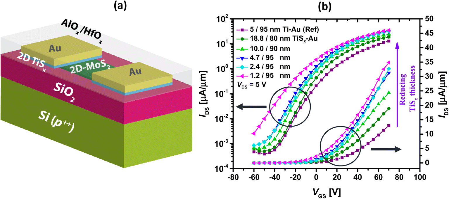 | ||
| Fig. 1 (a) Schematics of the fabricated MoS2 FETs, (b) measured transfer curves of the devices with series of TiSx contact thicknesses, in both semilog and linear scales. Data for the reference sample is also provided. | ||
The transfer curves (IDS–VGS) of the MoS2 FETs with different TiSx contact thicknesses are also provided in Fig. 1(b) and compared to the reference device. In all the cases, the current is measured on 500 nm long MoS2 channels and normalized to the device width (1 μm). At first sight, it is explicit that the entire series of TiSx-contacted devices outperform the reference case. In addition, reducing the TiSx thickness from 20 nm down to 1.2 nm improves the overall electrical performance. The maximum ON-state current (ION) increases to ∼35 μA μm−1 for the MoS2 FETs with the thinnest TiSx contacts, which is nearly three times higher than that of the reference. Furthermore, the threshold voltage (VT) shifts negatively with reducing the TiSx thickness, and the OFF-state current (IOFF) increases for the thinnest TiSx contacts of ∼1.2 nm, both implying an increase in the MoS2 doping level.12,70 Such doping effects have also been observed in previous studies where other 2D metallic contacts (e.g. graphene,36,38 NbS240 or VSe239 have been utilized. We note that in general, any kind of metal (2D or 3D bulk) dopes MoS2 or other 2D semiconductors up to a certain extent.41,61,70,71
For verifying the repeatability of the observations shown in Fig. 1(b), another set of MoS2 FETs with series of TiSx contact thicknesses were fabricated and characterized. Similar trends were observed for the second set upon reducing the TiSx contact thickness. See Fig. S1(a) and (b) in the ESI† and the associated discussion.
To further gain insight into the overall electrical performance of the MoS2 FETs with TiSx contacts, the average statistical data of ION, maximum μFE, IOFF and ON/OFF current ratio are provided in Fig. 2(a)–(d), respectively. The presented data were obtained by measuring three-four devices on each studied sample.
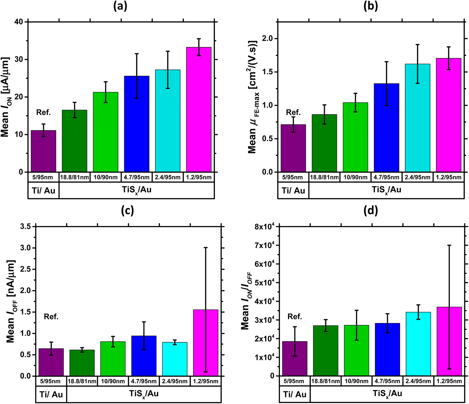 | ||
| Fig. 2 Average statistical data of (a) ION, (b) maximum μFE, (c) IOFF and (d) ON/OFF current ratio for the MoS2 FETs with various TiSx thicknesses, all obtained at VDS = 5 V. Data for the reference case with Ti/Au contacts is also included. | ||
In Fig. 2(a) and (b), ION and the maximum μFE show a monotonically increasing trend with reducing the TiSx thickness. In addition, the devices with the thickest TiSx contacts (∼20 nm) still outperform the reference devices of ∼5 nm Ti. Both values (ION and maximum μFE) also increase nearly twice on average when the TiSx thickness reduces to ∼1.2 nm. These observed device performance improvements by reducing the TiSx contact thickness can be mainly attributed to the reduction of the interfacial tunneling barrier within TiSx, which leads to a reduction in the TiSx overall interlayer resistance.61 In fact, because layers in 2D TMDCs are generally held by weak vdW forces, a gap is always present in between the individual layers. This gap acts as an interfacial tunneling barrier that scatters carriers, degrades the current and contributes to Rc.41,61,72,73 Therefore, when the number of layers in a 2D metallic TiSx reduces, the interfacial tunneling barrier and the resulting interlayer resistance are expected to reduce. In addition to that, the Au electrodes get closer to the MoS2 active layers, altogether leading to a more efficient carrier injection/collection and hence improvements in the ON-state device characteristics. The overall superior performance of the TiSx-contacted MoS2 FETs to the reference devices can also be associated with the reduced perturbance of the MoS2 electronic band-structure,45 when the 3D bulk metallic contacts (Ti) are replaced with the 2D TiSx counterparts.
Fig. 2(c) shows the average trend for IOFF. As can be seen, there is no significant change in this metric with reducing the TiSx thickness, except for when ∼1.2 nm TiSx contacts are employed. The rise of IOFF in this case can be associated with the increased electrostatic doping in MoS2, such that higher back-gate voltages are required to fully deplete the channel in the OFF-state regime. However, because IOFF is maintained well below 2 μA μm−1, a similar ON/OFF current ratio in the range of 104 (Fig. 2(d)) is achieved for all the studied cases. It is worthwhile mentioning that IOFF can be further controlled if a thinner back-gate oxide (e.g. 30 nm SiO2) is employed, as thinner SiO2 typically leads to improved electrostatic control over the MoS2 channel.
Based on the analyses provided so far, the MoS2 FETs with ∼1.2 nm thick TiSx contacts were found to be the most optimally operating devices. To confirm this further, the electrical performance of the second set of MoS2 devices with various TiSx contact thicknesses were also statistically evaluated. See Fig. S1(a)–(d) in the ESI.† Our analyses verify that the MoS2 devices with ∼1.2 nm thick TiSx contacts still lead to the most optimal performance. Therefore, they were selected for further electrical characterization.
The Rc of such devices were evaluated in the next step and compared to that of the reference case. To extract Rc, transfer length method (TLM) structures74 of various MoS2 channel lengths (ranging from 0.5–5 μm) were electrically measured, and the total resistance (Rtot) of both TiSx and Ti contacts were extracted from the transfer curves. Fig. 3(a) and (b) show the layout TLM design and the optical image of the probed TLM structures used for the I–V measurements, respectively. A low VDS voltage (VDS = 0.5 V) was applied for the Rc evaluations. This was to minimize the errors occurring during the Rc extraction, as the application of high VDS (VDS > 1 V) resulted in negative Rc and its underestimation. The Rc values were obtained using the following formula, where the dependence of the individual parameters on the applied VGS is also included:74,75
| Rtot(VGS) = 2 × Rc(VGS) + Rsh(VGS) × (L/W) | (1) |
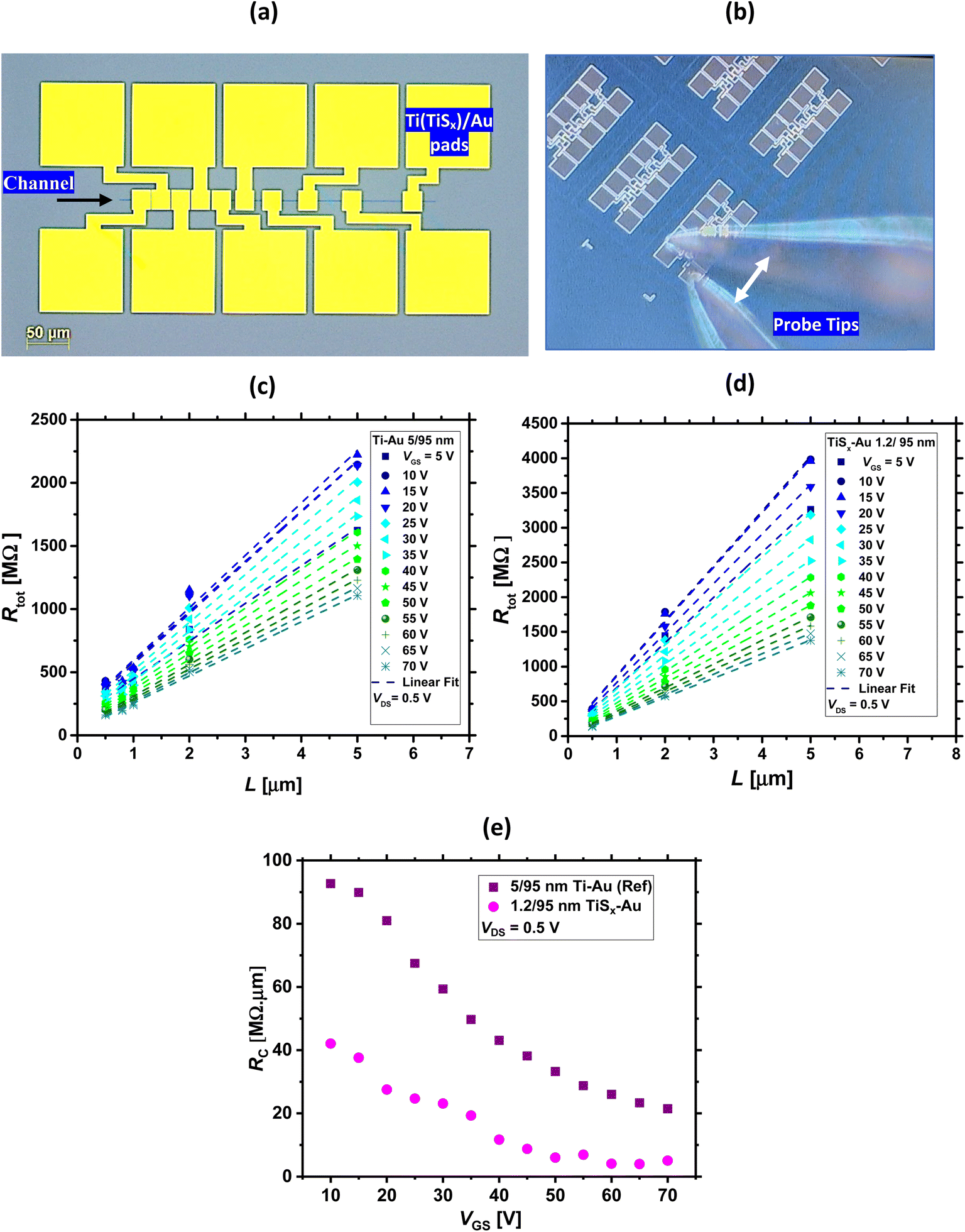 | ||
| Fig. 3 (a) Top-view TLM layout design used for Rc extractions, with a channel width of 1 μm and various channel lengths ranging from 0.5–50 μm. As indicated, yellow squares are the Ti(TiSx)/Au contact pads. (b) Optical image of the probed TLM structures used for the I–V measurements. The white arrow indicates the probe tips. (c) and (d) Rtotversus L for the MoS2 FETs with TiSx/Au and Ti/Au contacts, respectively (at VDS = 0.5 V and for different VGS). (e) Extracted Rc as a function of VGS for the TiSx/Au and Ti/Au cases. | ||
Fig. 3(c) and (d) display Rtot as a function of L for the TiSx contacts and the reference case, respectively, at VDS = 0.5 V and for different VGS values. Using these plots, Rc can be extracted.74 This is provided in Fig. 3(e). As can be seen, at VGS = 70 V, the Rc for the TiSx-contacted MoS2 FETs is ∼5.0 MΩ μm and nearly four times smaller than that of the reference (which is 21.4 MΩ μm). These values of Rc are still higher than what is obtained for FETs fabricated from exfoliated/CVD grown highly crystalline MoS2, which may be due to the nanocrystalline nature of our films and their average grain size of 70 nm.57 However, the replacement of 3D bulk Ti contacts with the 2D TiSx counterparts is overall beneficial in reducing Rc of the ALD-based MoS2 FETs.
One might also wonder about the Rsh of the ALD-based MoS2. It is worthwhile mentioning that for having an accurate estimation of Rsh, 4-wire measurements76 as well as models specifically tailored for 2D polycrystalline materials77,78 need to be employed.
The SBH is another important factor for evaluating the contact quality in 2D-based FETs. The carrier transport across a Schottky junction can be described by thermionic emission equation modified for 2D materials:21,79
 | (2) |
 is the 2D equivalent Richardson constant, T is temperature, q is the elementary charge magnitude, kB is the Boltzmann constant, φBn is the effective barrier height for electrons and η is the ideality factor. To determine φBn of both TiSx and Ti contacts to MoS2, low-temperature I–V measurements were carried out. The output data (IDS–VDS) were obtained for various VGS (ranging from −10 V to +60 V), at seven different temperatures (180–290 K). A first order approximation of eqn (2) was used,81 which is expressed as the following:
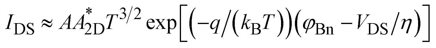 | (3) |
For a fixed VGS, ln(IDS/T3/2) versus 1000/T is first plotted at each measured VDS, and a series of Arrhenius plots are obtained. This is shown in Fig. 4(a) and (b) for both Ti/Au and TiSx/Au cases, respectively. As can be seen, the acquired data are linear in each VDS. If the slope of the individual fitted lines are plotted as a function of VDS, as illustrated in Fig. 4(c) and (d) for both the TiSx and Ti cases, the interception point with the vertical axis (S0) yields φBn for a fixed VGS.80,81S0 is related to φBn through the following equation:81
| S0 = (−qφBn)/(1000kB) | (4) |
 | ||
| Fig. 4 Arrhenius plots for (a) Ti/Au and (b) TiSx/Au contacts to MoS2 at VGS = 0 V, (c) and (d) extracted slopes from (a) and (b) as a function of VDS, at VGS = 0 V. The vertical axis-intercept (S0) yields φBn at VGS = 0 V. | ||
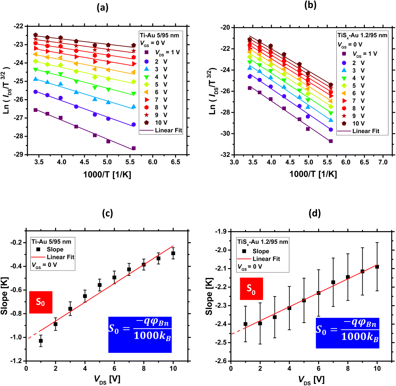
If the above-mentioned extractions are repeated for each measured VGS, φBn as a function of VGS can be obtained. The final results are shown in Fig. 5(a). As evidenced from this figure, φBn varies linearly at low VGS ranges (the fitted straight line). Then, it starts to deviate from the linearity at a certain VGS. In fact, the thermionic emission equation is valid only for VGS below the flat-band potential (VFB).23 Above VFB, in addition to the thermionic emission, the tunneling emission contributes to the total current, leading to the observed deviation from the linear trend.14
 | ||
| Fig. 5 (a) Effective Schottky barrier height (φBn) as a function of VGS for both Ti/Au and TiSx/Au contacts to MoS2 FETs. Below the flat band condition, φBn reduces linearly with increasing VGS, which is marked by the fitted straight lines in both contact cases, (b) energy band diagrams of Ti, sulfur-deficient TiSx62 and Au with respect to MoS2. | ||
Fig. 5(a) also compares the contact metal types. For all the measured VGS, φBn is higher for the TiSx contacts (270–132 meV) than for the Ti counterparts (123–35 meV). This is expected, as TiSx is theoretically predicted to have higher WF than Ti. To illustrate this concept, the energy band diagrams of Ti, TiSx and Au are schematically depicted in Fig. 5(b).
Despite a higher φBn, the TiSx contacts to MoS2 exhibit lower Rc than the Ti counterparts (Fig. 3(e)). Therefore, the observed Rc reduction in the TiSx-contacted devices is mostly associated with an increase in the MoS2 electrostatic doping level, which could be due to the achievement of a flat/clean interface at the junction upon replacing the 3D Ti contacts with the 2D TiSx counterparts, such that the carriers are injected more efficiently into the MoS2 channel. The increase in the MoS2 n-type doping level is evidenced from the negative shift of VT (Fig. 1(b)) and the slight increase of IOFF (Fig. 1(b) and 2(c)), once the Ti contacts are replaced with ∼1.2 nm of TiSx. For high doping levels, the width of the SB reduces,23 and the carrier tunneling towards MoS2 further facilitates, leading to an overall increase in the current. In such a situation, the height of the SB (φBn) will have a smaller effect on the overall device performance.
Considering TiSx contacted MoS2 FETs, one might find the observations contradictory to the energy band diagram analysis, as high WF metals (such as TiSx) are expected to dope MoS2 to p-type. Recent density functional theory (DFT) calculations by Gao et al.61 have addressed this controversy and have shown that TiS2 can act as both p- or n-type contact to MoS2, depending on the TiS2 number of layers and the doping concentration of both materials. TiS2 can also tune the barrier height at the junction, and it is predicted that for n-type 2L-TiS2 (∼1.2 nm) contacts to MoS2, the barrier height for electrons is two-times smaller than for holes. Hence, in contrast to the current band theory, it is possible to ignore p-type doping of MoS2 by TiSx contacts. Similar experimental observations were also reported by Bark et al.40 when replacing 3D Mo contacts (WF ∼ 4.5 eV) with high WF 2D NbS2 contacts (WF ∼ 6.1 eV)45 in MoS2 FETs. These studies indicate that there is a clear distinction between 3D and 2D metals contacting 2D semiconductors.
It is also worthwhile mentioning that for ultrathin layers of 2D TiSx, quantum confinement effects start to play a role, which can affect the TiSx electronic band structure and its alignment to that of MoS2 at the interface. Hence, providing a more realistic picture of the TiSx/MoS2 energy band diagrams may require additional DFT simulations.
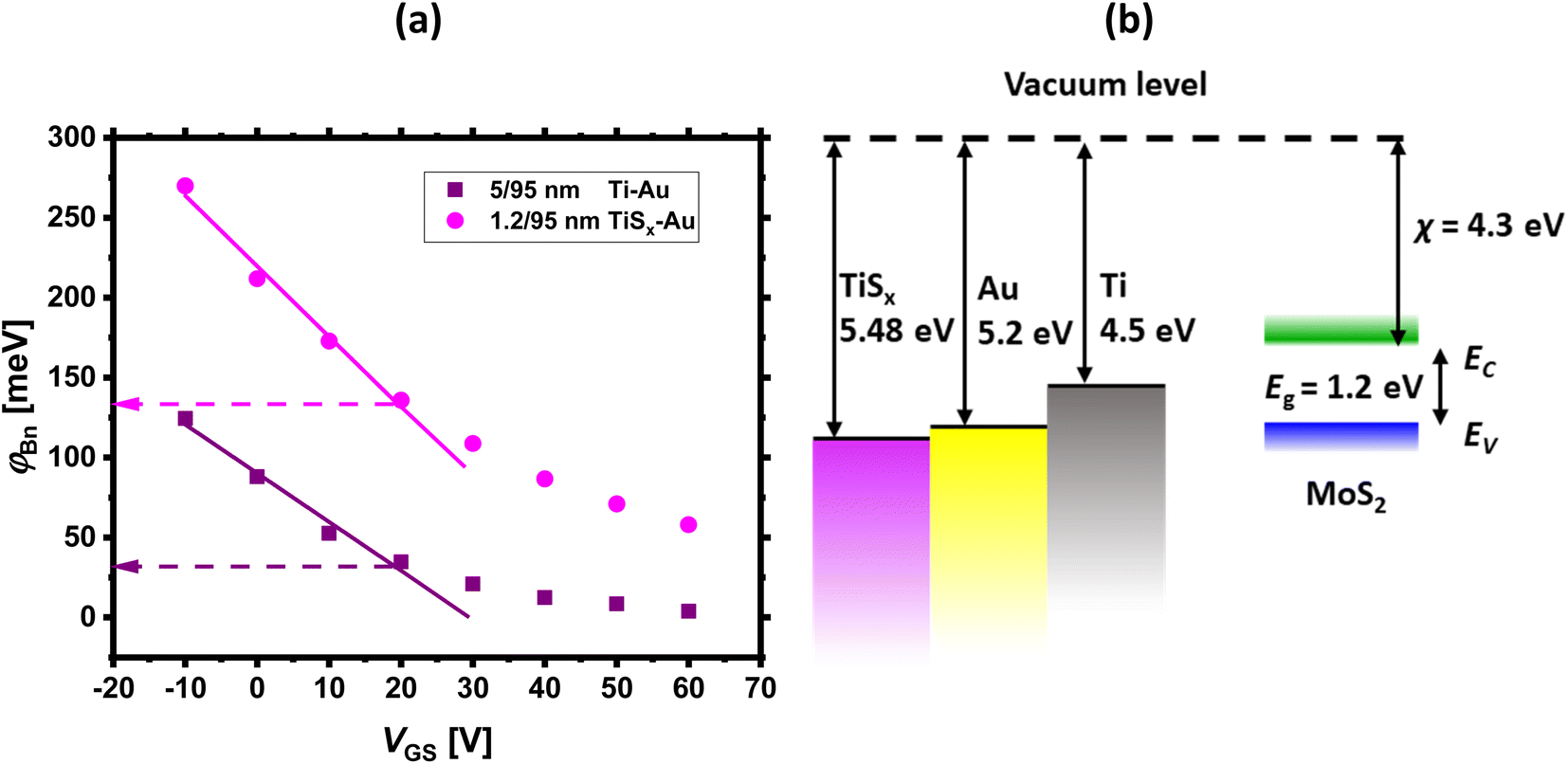
To further understand the discrepancies between the 2D and 3D metals contacting a 2D TMDC semiconductor and to verify our experimental results, TCAD simulations were also performed for the 2D TiS2 and 3D Ti contacts to MoS2. The simulated device had a channel length of 500 nm and consisted of 1.2 nm of MoS2, 5 nm of Ti and 1.2 nm of TiS2. Selection of 1.2 nm TiS2 was because this thickness led to the most optimally performing MoS2 FETs in our experiments. The biasing conditions were VDS = 1 V and VGS = 30 V, to ensure that both device types are fully in their ON-state regime. Further details regarding the simulation parameters are provided in the ESI, Section S.3.† The resultant 2D contour plots of the gate-field-induced charge carrier density and the current density are displayed in Fig. 6(a)–(d), respectively. We note that Au contact pads are not shown in these figures.
 | ||
| Fig. 6 (a and b) 2D contour plots of the induced charge carrier density and (c and d) current density for Ti and TiS2 contacts to MoS2, respectively. Simulations were performed for 1.2 nm of MoS2, 5 nm of Ti and 1.2 nm of TiS2 at VDS = 1 V and VGS = 30 V. | ||
As can be seen from Fig. 6(a) and (b), when TiS2 is in contact with MoS2, more charges are induced into the channel and MoS2 is doped to a higher extent, compared to the Ti case. The increase in the induced charge carrier density close to the contact regions can be distinguished by the dark orange color. As anticipated, the transverse field-induced carrier formation can be observed at the TiS2–MoS2 interface as well. Comparing Fig. 6(c) and (d), an increase in the MoS2 current density can be noted for the case of TiS2. In fact, only a small portion of TiS2 is actively in contact with MoS2, which facilitates the charge transport and subsequently leads to improved current density as well as the overall reduction of Rc. The provided simulation results well confirm the experimental observations and highlight the importance of integrating 2D metallic contacts with 2D semiconductors in 2D-based FETs.
Conclusions
To conclude, in this study, we have investigated the integration of 2D metallic TiSx with semiconducting 2D MoS2 by using atomic layer deposition (ALD). We have shown that ALD grown TiSx (x ∼ 1.8) contacts can improve the overall electrical performance of ALD-based MoS2 FETs, when employed as the contacts to polycrystalline MoS2 films. Based on our analyses, only ∼1.2 nm of ALD grown TiSx is sufficient for unleashing the most from the electrical capabilities of ALD-based MoS2 FETs. Utilization of TiSx contacts improved the average ON-state device characteristics and led to the achievement of ION as high as ∼35 μA μm−1. In addition and despite a higher Schottky barrier height, TiSx contacts reduced the Rc of the fabricated MoS2 FETs down to ∼5.0 MΩ μm, which is nearly a quarter of what was obtained for the bulk Ti contacts (21.4 MΩ μm).Data availability
The data that support the findings of this study are available from the corresponding author upon request.Conflicts of interest
The authors declare no competing financial interest.Acknowledgements
This work is funded by the European research council (ERC) under the grant Agreement No. 648787-ALDof2DTMDs. The authors would like to acknowledge the NanoLab TU/e for the cleanroom facilities as well as the technical support of E. J. Geluk, B. Krishnamoorthy, M. G. Dijstelbloem, P. P. P. Bax, T. de Vries, C. V. Helvoirt, J. J. A. Zeebregts and W. M. Dijkstra. Further, R. M. would like to express her special gratitude to Prof. Dr J. P. Hofmann and Y. Zhang from the laboratory of inorganic materials and catalysis (Department of Chemical Engineering and Chemistry, TU/e) for sulfurizing the MoOx samples in their home-built tube furnace, Dr S. B. Basuvalingam and J. J. P. M. Schulpen for scientific and practical discussions, M. A. Taheri (founder of Cosmointel Inc.) for graciously enabling access to T-consciousness fields used in this work, Molecular Materials and Nano-systems (M2N) research group (Department of Applied Physics, TU/e) for supplying resources to conduct the electrical measurements as well as SMART Photonics to provide access to their glove box for sample storage. A. A. S. would also like to thank NWO, The Netherlands, SERB (SERB/2017/1562) India, and SRMIST for the financial support and research funding.References
- S. Manzeli, D. Ovchinnikov, D. Pasquier, O. V. Yazyev and A. Kis, Nat. Rev. Mater., 2017, 2, 17033 CrossRef CAS.
- M. Chhowalla, D. Jena and H. Zhang, Nat. Rev. Mater., 2016, 1, 16052 CrossRef CAS.
- A. K. Geim and I. V Grigorieva, Nature, 2013, 499, 419–425 CrossRef CAS PubMed.
- R. Ganatra and Q. Zhang, ACS Nano, 2014, 8, 4074–4099 CrossRef CAS PubMed.
- B. Radisavljevic, A. Radenovic, J. Brivio, V. Giacometti and A. Kis, Nat. Nanotechnol., 2011, 6, 147–150 CrossRef CAS PubMed.
- C. J. McClellan, E. Yalon, K. K. H. Smithe, S. V. Suryavanshi and E. Pop, ACS Nano, 2021, 15, 1587–1596 CrossRef CAS PubMed.
- Y. Liu, J. Guo, Y. Wu, E. Zhu, N. O. Weiss, Q. He, H. Wu, H. C. Cheng, Y. Xu, I. Shakir, Y. Huang and X. Duan, Nano Lett., 2016, 16, 6337–6342 CrossRef CAS PubMed.
- P.-C. Shen, C. Su, Y. Lin, A.-S. Chou, C.-C. Cheng, J.-H. Park, M.-H. Chiu, A.-Y. Lu, H.-L. Tang, M. M. Tavakoli, G. Pitner, X. Ji, Z. Cai, N. Mao, J. Wang, V. Tung, J. Li, J. Bokor, A. Zettl, C.-I. Wu, T. Palacios, L.-J. Li and J. Kong, Nature, 2021, 593, 211–217 CrossRef CAS PubMed.
- Y. Y. Illarionov, K. K. H. Smithe, M. Waltl, T. Knobloch, E. Pop and T. Grasser, IEEE Electron Device Lett., 2017, 38, 1763–1766 CAS.
- A. Leonhardt, D. Chiappe, V. V. Afanas’ev, S. El Kazzi, I. Shlyakhov, T. Conard, A. Franquet, C. Huyghebaert and S. de Gendt, ACS Appl. Mater. Interfaces, 2019, 11, 42697–42707 CrossRef CAS PubMed.
- W. Li, J. Zhou, S. Cai, Z. Yu, J. Zhang, N. Fang, T. Li, Y. Wu, T. Chen, X. Xie, H. Ma, K. Yan, N. Dai, X. Wu, H. Zhao, Z. Wang, D. He, L. Pan, Y. Shi, P. Wang, W. Chen, K. Nagashio, X. Duan and X. Wang, Nat. Electron., 2019, 2, 563–571 CrossRef CAS.
- P. Bolshakov, C. M. Smyth, A. Khosravi, P. Zhao, P. K. Hurley, C. L. Hinkle, R. M. Wallace and C. D. Young, ACS Appl. Electron. Mater., 2019, 1, 210–219 CrossRef CAS.
- K. Kang, S. Xie, L. Huang, Y. Han, P. Y. Huang, K. F. Mak, C.-J. Kim, D. Muller and J. Park, Nature, 2015, 520, 656–660 CrossRef CAS PubMed.
- S. Das, H.-Y. Chen, A. V. Penumatcha and J. Appenzeller, Nano Lett., 2013, 13, 100–105 CrossRef CAS PubMed.
- K. K. H. Smithe, S. V. Suryavanshi, M. Muñoz Rojo, A. D. Tedjarati and E. Pop, ACS Nano, 2017, 11, 8456–8463 CrossRef CAS PubMed.
- B. Radisavljevic, M. B. Whitwick and A. Kis, ACS Nano, 2011, 5, 9934–9938 CrossRef CAS PubMed.
- S. Wachter, D. K. Polyushkin, O. Bethge and T. Mueller, Nat. Commun., 2017, 8, 14948 CrossRef CAS PubMed.
- C. Huyghebaert, T. Schram, Q. Smets, T. Kumar Agarwal, D. Verreck, S. Brems, A. Phommahaxay, D. Chiappe, S. El Kazzi, C. Lockhart de la Rosa, G. Arutchelvan, D. Cott, J. Ludwig, A. Gaur, S. Sutar, A. Leonhardt, D. Marinov, D. Lin, M. Caymax, I. Asselberghs, G. Pourtois and I. P. Radu, IEEE International Electron Devices Meeting (IEDM), 2018, DOI:10.1109/IEDM.2018.8614679.
- A. Afzalian, npj 2D Mater. Appl., 2021, 5, 5 CrossRef CAS.
- K. Alam and R. K. Lake, IEEE Trans. Electron Devices, 2012, 59, 3250–3254 CAS.
- A. Allain, J. Kang, K. Banerjee and A. Kis, Nat. Mater., 2015, 14, 1195–1205 CrossRef CAS PubMed.
- IEEE International Roadmap for Devices and Systems - IEEE IRDS™, https://irds.ieee.org Search PubMed.
- S. M. Sze and K. K. Ng, Physics of Semiconductor Devices, John Wiley & Sons, Inc., Hoboken, NJ, USA, 2006 Search PubMed.
- Y. Taur and T. H. Ning, Fundamentals of Modern VLSI Devices, Cambridge University Press, 2009 Search PubMed.
- H.-J. Chuang, B. Chamlagain, M. Koehler, M. M. Perera, J. Yan, D. Mandrus, D. Tománek and Z. Zhou, Nano Lett., 2016, 16, 1896–1902 CrossRef CAS PubMed.
- K. Heo, S.-H. Jo, J. Shim, D.-H. Kang, J.-H. Kim and J.-H. Park, ACS Appl. Mater. Interfaces, 2018, 10, 32765–32772 CrossRef CAS PubMed.
- R. Kappera, D. Voiry, S. E. Yalcin, B. Branch, G. Gupta, A. D. Mohite and M. Chhowalla, Nat. Mater., 2014, 13, 1128–1134 CrossRef CAS PubMed.
- S. Lee, A. Tang, S. Aloni and H.-S. Philip Wong, Nano Lett., 2016, 16, 276–281 CrossRef CAS PubMed.
- W. Park, Y. Kim, S. K. Lee, U. Jung, J. Ho Yang, C. Cho, Y. Ji Kim, S. K. Lim, I. S. Hwang, H.-B.-R. Lee and B. H. Lee, 2014 IEEE International Electron Devices Meeting, 2014, DOI:10.1109/IEDM.2014.7046986.
- A. Alharbi and D. Shahrjerdi, IEEE Trans. Electron Devices, 2018, 65, 4084–4092 CAS.
- K. Parto, A. Pal, T. Chavan, K. Agashiwala, C.-H. Yeh, W. Cao and K. Banerjee, Phys. Rev. Appl., 2021, 15, 1–17 Search PubMed.
- M. H. D. Guimarães, H. Gao, Y. Han, K. Kang, S. Xie, C.-J. Kim, D. A. Muller, D. C. Ralph and J. Park, ACS Nano, 2016, 10, 6392–6399 CrossRef PubMed.
- X. Cui, G.-H. Lee, Y. D. Kim, G. Arefe, P. Y. Huang, C.-H. Lee, D. A. Chenet, X. Zhang, L. Wang, F. Ye, F. Pizzocchero, B. S. Jessen, K. Watanabe, T. Taniguchi, D. A. Muller, T. Low, P. Kim and J. Hone, Nat. Nanotechnol., 2015, 10, 534–540 CrossRef CAS PubMed.
- W. S. Leong, Q. Ji, N. Mao, Y. Han, H. Wang, A. J. Goodman, A. Vignon, C. Su, Y. Guo, P.-C. Shen, Z. Gao, D. A. Muller, W. A. Tisdale and J. Kong, J. Am. Chem. Soc., 2018, 140, 12354–12358 CrossRef CAS PubMed.
- Y. Liu, H. Wu, H. C. Cheng, S. Yang, E. Zhu, Q. He, M. Ding, D. Li, J. Guo, N. O. Weiss, Y. Huang and X. Duan, Nano Lett., 2015, 15, 3030–3034 CrossRef CAS PubMed.
- S. S. Chee, D. Seo, H. Kim, H. Jang, S. Lee, S. P. Moon, K. H. Lee, S. W. Kim, H. Choi and M. H. Ham, Adv. Mater., 2019, 31, 1–7 CrossRef PubMed.
- W. S. Leong, X. Luo, Y. Li, K. H. Khoo, S. Y. Quek and J. T. L. Thong, ACS Nano, 2015, 9, 869–877 CrossRef CAS PubMed.
- Y. Du, L. Yang, J. Zhang, H. Liu, K. Majumdar, P. D. Kirsch and P. D. Ye, IEEE Electron Device Lett., 2014, 35, 599–601 CAS.
- J. Li, X. Yang, Y. Liu, B. Huang, R. Wu, Z. Zhang, B. Zhao, H. Ma, W. Dang, Z. Wei, K. Wang, Z. Lin, X. Yan, M. Sun, B. Li, X. Pan, J. Luo, G. Zhang, Y. Liu, Y. Huang, X. Duan and X. Duan, Nature, 2020, 579, 368–374 CrossRef CAS PubMed.
- H. Bark, Y. Choi, J. Jung, J. H. Kim, H. Kwon, J. Lee, Z. Lee, J. H. Cho and C. Lee, Nanoscale, 2018, 10, 1056–1062 RSC.
- J. Kang, W. Liu, D. Sarkar, D. Jena and K. Banerjee, Phys. Rev. X, 2014, 4, 031005 CAS.
- C. Gong, L. Colombo, R. M. Wallace and K. Cho, Nano Lett., 2014, 14, 1714–1720 CrossRef CAS PubMed.
- C. Kim, I. Moon, D. Lee, M. S. Choi, F. Ahmed, S. Nam, Y. Cho, H.-J. Shin, S. Park and W. J. Yoo, ACS Nano, 2017, 11, 1588–1596 CrossRef CAS PubMed.
- M. Farmanbar and G. Brocks, Adv. Electron. Mater., 2016, 2, 1500405 CrossRef.
- Y. Liu, P. Stradins and S. H. Wei, Sci. Adv., 2016, 2, 1–7 Search PubMed.
- Y. J. Yu, Y. Zhao, S. Ryu, L. E. Brus, K. S. Kim and P. Kim, Nano Lett., 2009, 9, 3430–3434 CrossRef CAS PubMed.
- H. Ago, IEEE International Symposium on VLSI Technology, Systems and Applications (VLSI-TSA), 2020, DOI:10.1109/VLSI-TSA48913.2020.9203747.
- Y.-H. Lee, X.-Q. Zhang, W. Zhang, M.-T. Chang, C.-T. Lin, K.-D. Chang, Y.-C. Yu, J. T.-W. Wang, C.-S. Chang, L.-J. Li and T.-W. Lin, Adv. Mater., 2012, 24, 2320–2325 CrossRef CAS PubMed.
- D. Chiappe, J. Ludwig, A. Leonhardt, S. El Kazzi, A. Nalin Mehta, T. Nuytten, U. Celano, S. Sutar, G. Pourtois, M. Caymax, K. Paredis, W. Vandervorst, D. Lin, S. De Gendt, K. Barla, C. Huyghebaert, I. Asselberghs and I. Radu, Nanotechnology, 2018, 29, 425602 CrossRef PubMed.
- T. Kim, J. Mun, H. Park, D. Joung, M. Diware, C. Won, J. Park, S.-H. Jeong and S.-W. Kang, Nanotechnology, 2017, 28, 18LT01 CrossRef PubMed.
- Y. Zhan, Z. Liu, S. Najmaei, P. M. Ajayan and J. Lou, Small, 2012, 8, 966–971 CrossRef CAS PubMed.
- Z.-L. Tian, D.-H. Zhao, H. Liu, H. Zhu, L. Chen, Q.-Q. Sun and D. W. Zhang, ACS Appl. Nano Mater., 2019, 2, 7810–7818 CrossRef CAS.
- W. Jeon, Y. Cho, S. Jo, J. H. Ahn and S. J. Jeong, Adv. Mater., 2017, 29, 1–8 Search PubMed.
- J. J. Pyeon, I.-H. Baek, W. C. Lim, K. H. Chae, S. H. Han, G. Y. Lee, S.-H. Baek, J.-S. Kim, J.-W. Choi, T.-M. Chung, J. H. Han, C.-Y. Kang and S. K. Kim, Nanoscale, 2018, 10, 17712–17721 RSC.
- J.-G. Song, J. Park, W. Lee, T. Choi, H. Jung, C. W. Lee, S.-H. Hwang, J. M. Myoung, J.-H. Jung, S.-H. Kim, C. Lansalot-Matras and H. Kim, ACS Nano, 2013, 7, 11333–11340 CrossRef CAS PubMed.
- S. B. Basuvalingam, M. A. Bloodgood, M. A. Verheijen, W. M. M. Kessels and A. A. Bol, ACS Appl. Nano Mater., 2021, 4, 514–521 CrossRef CAS PubMed.
- A. Sharma, R. Mahlouji, L. Wu, M. A. Verheijen, V. Vandalon, S. Balasubramanyam, J. P. Hofmann, W. M. M. (Erwin) Kessels and A. A. Bol, Nanotechnology, 2020, 31, 255603 CrossRef CAS PubMed.
- S. M. George, Chem. Rev., 2010, 110, 111–131 CrossRef CAS PubMed.
- H. B. Profijt, S. E. Potts, M. C. M. van de Sanden and W. M. M. Kessels, J. Vac. Sci. Technol., A, 2011, 29, 050801 CrossRef.
- C. S. Cucinotta, K. Dolui, H. Pettersson, Q. M. Ramasse, E. Long, S. E. O'Brian, V. Nicolosi and S. Sanvito, J. Phys. Chem. C, 2015, 119, 15707–15715 CrossRef CAS.
- J. Gao and M. Gupta, npj 2D Mater. Appl., 2020, 4, 1–9 CrossRef.
- T. Das, S. Chakraborty, R. Ahuja and G. P. Das, ChemPhysChem, 2019, 20, 608–617 CrossRef CAS PubMed.
- G. Yin, H. Zhao, J. Feng, J. Sun, J. Yan, Z. Liu, S. Lin and S. (Frank) Liu, J. Mater. Chem. A, 2018, 6, 9132–9138 RSC.
- M. F. J. Vos, B. Macco, N. F. W. Thissen, A. A. Bol and W. M. M. (Erwin) Kessels, J. Vac. Sci. Technol., A, 2016, 34, 01A103 CrossRef.
- R. Mahlouji, M. A. Verheijen, Y. Zhang, J. P. Hofmann, W. M. M. Kessels and A. A. Bol, Adv. Electron. Mater., 2022, 8, 2100781 CrossRef CAS.
- S. B. Basuvalingam, Y. Zhang, M. A. Bloodgood, R. H. Godiksen, A. G. Curto, J. P. Hofmann, M. A. Verheijen, W. M. M. Kessels and A. A. Bol, Chem. Mater., 2019, 31, 9354–9362 CrossRef CAS PubMed.
- R. Mahlouji, Y. Zhang, M. A. Verheijen, J. P. Hofmann, W. M. M. Kessels, A. A. Sagade and A. A. Bol, ACS Appl. Electron. Mater., 2021, 3, 3185–3199 CrossRef CAS PubMed.
- K. B. Jinesh, J. L. van Hemmen, M. C. M. van de Sanden, F. Roozeboom, J. H. Klootwijk, W. F. A. Besling and W. M. M. Kessels, J. Electrochem. Soc., 2011, 158, G21 CrossRef CAS.
- A. Sharma, V. Longo, M. A. Verheijen, A. A. Bol and W. M. M. (Erwin) Kessels, J. Vac. Sci. Technol., A, 2017, 35, 01B130 CrossRef.
- K. Schauble, D. Zakhidov, E. Yalon, S. Deshmukh, R. W. Grady, K. A. Cooley, C. J. McClellan, S. Vaziri, D. Passarello, S. E. Mohney, M. F. Toney, A. K. Sood, A. Salleo and E. Pop, ACS Nano, 2020, 14, 14798–14808 CrossRef CAS PubMed.
- Y. Kim, A. R. Kim, J. H. Yang, K. E. Chang, J.-D. Kwon, S. Y. Choi, J. Park, K. E. Lee, D.-H. Kim, S. M. Choi, K. H. Lee, B. H. Lee, M. G. Hahm and B. Cho, Nano Lett., 2016, 16, 5928–5933 CrossRef CAS PubMed.
- S. Das and J. Appenzeller, Nano Lett., 2013, 13, 3396–3402 CrossRef CAS PubMed.
- S. Das and J. Appenzeller, Phys. Status Solidi RRL, 2013, 7, 268–273 CrossRef CAS.
- D. K. Schroder, Semiconductor Material and Device Characterization, John Wiley & Sons, Inc., Hoboken, NJ, USA, 2005 Search PubMed.
- S. B. Mitta, M. S. Choi, A. Nipane, F. Ali, C. Kim, J. T. Teherani, J. Hone and W. J. Yoo, 2D Mater., 2021, 8, 012002 CrossRef CAS.
- I. Miccoli, F. Edler, H. Pfnür and C. Tegenkamp, J. Phys.: Condens. Matter, 2015, 27, 223201 CrossRef CAS PubMed.
- H. Park, J. Lee, C.-J. Lee, J. Kang, J. Yun, H. Noh, M. Park, J. Lee, Y. Park, J. Park, M. Choi, S. Lee and H. Park, Nanomaterials, 2022, 12, 206 CrossRef CAS PubMed.
- S. Y. Min, C. Cho, G. W. Shim, I.-J. Park, D. Y. Jung, Y. Woo, J.-Y. Lee and S.-Y. Choi, FlatChem, 2018, 7, 19–25 CrossRef CAS.
- A. Anwar, B. Nabet, J. Culp and F. Castro, J. Appl. Phys., 1999, 85, 2663–2666 CrossRef CAS.
- K. Cho, J. Pak, J.-K. Kim, K. Kang, T.-Y. Kim, J. Shin, B. Y. Choi, S. Chung and T. Lee, Adv. Mater., 2018, 30, 1705540 CrossRef PubMed.
- J.-R. Chen, P. M. Odenthal, A. G. Swartz, G. C. Floyd, H. Wen, K. Y. Luo and R. K. Kawakami, Nano Lett., 2013, 13, 3106–3110 CrossRef CAS PubMed.
Footnote |
| † Electronic supplementary information (ESI) available. See DOI: https://doi.org/10.1039/d3na00387f |
| This journal is © The Royal Society of Chemistry 2023 |