
 Open Access Article
 This Open Access Article is licensed under a Creative Commons Attribution-Non Commercial 3.0 Unported Licence
Growth mechanisms of monolayer hexagonal boron nitride (h-BN) on metal surfaces: theoretical perspectives
Md. Sherajul
Islam
 *ad,
Abdullah Al Mamun
Mazumder
b,
Minhaz Uddin
Sohag
a,
Md. Mosarof Hossain
Sarkar
a,
Catherine
Stampfl
c and
Jeongwon
Park
de
*ad,
Abdullah Al Mamun
Mazumder
b,
Minhaz Uddin
Sohag
a,
Md. Mosarof Hossain
Sarkar
a,
Catherine
Stampfl
c and
Jeongwon
Park
de
aDepartment of Electrical and Electronic Engineering, Khulna University of Engineering & Technology, Khulna 9203, Bangladesh. E-mail: sheraj_kuet@eee.kuet.ac.bd
bDepartment of Electrical Engineering, University of South Carolina, Columbia, SC 29208, USA
cSchool of Physics, The University of Sydney, New South Wales 2006, Australia
dDepartment of Electrical and Biomedical Engineering, University of Nevada, Reno, NV 89557, USA
eSchool of Electrical Engineering and Computer Science, University of Ottawa, Ottawa, ON K1N 6N5, Canada
First published on 17th July 2023
Abstract
Two-dimensional hexagonal boron nitride (h-BN) has appeared as a promising material in diverse areas of applications, including as an excellent substrate for graphene devices, deep-ultraviolet emitters, and tunneling barriers, thanks to its outstanding stability, flat surface, and wide-bandgap. However, for achieving such exciting applications, controllable mass synthesis of high-quality and large-scale h-BN is a precondition. The synthesis of h-BN on metal surfaces using chemical vapor deposition (CVD) has been extensively studied, aiming to obtain large-scale and high-quality materials. The atomic-scale growth process, which is a prerequisite for rationally optimizing growth circumstances, is a key topic in these investigations. Although theoretical investigations on h-BN growth mechanisms are expected to reveal numerous new insights and understandings, different growth methods have completely dissimilar mechanisms, making theoretical research extremely challenging. In this article, we have summarized the recent cutting-edge theoretical research on the growth mechanisms of h-BN on different metal substrates. On the frequently utilized Cu substrate, h-BN development was shown to be more challenging than a simple adsorption-dehydrogenation-growth scenario. Controlling the number of surface layers is also an important challenge. Growth on the Ni surface is controlled by precipitation. An unusual reaction-limited aggregation growth behavior has been seen on interfaces having a significant lattice mismatch to h-BN. With intensive theoretical investigations employing advanced simulation approaches, further progress in understanding h-BN growth processes is predicted, paving the way for guided growth protocol design.
1. Introduction
In the last decade, several scientific breakthroughs have been made in two-dimensional (2D) materials,1–5 including graphene,6–19 hexagonal boron nitride (h-BN),20–48 transition-metal dichalcogenides (TMDCs),49–66 layered double hydroxides (LDHs),67–74 metal–organic frameworks (MOFs),75–79 black phosphorus (BP),80–87 and so many others.88–116 In particular, 2D h-BN, a geometrical analogue to graphene, is extensively studied due to its distinctive chemical and physical features. Despite the possibility that the lattice characteristics of h-BN are identical to those of carbon, the distinct constituent components give it highly diverse physical properties. Most notably, h-BN has significantly better chemical and thermal reliabilities (up to 1000 °C in atmosphere and 1400 °C in vacuum),117 improved oxidation resistance,118 and outstanding optical characteristics,119 while also having a similar excellent thermal conductivity (∼484 W m−1 K−1) and exceptional mechanical behavior (Young's modulus ∼1.0 TPa and elastic constant of 220–510 N m−1).42,120,121 In contrast to graphene, h-BN exhibits considerably different electrical characteristics. The wide bandgap of ∼5.9 eV (ref. 122 and 123) makes h-BN an electrical insulator, whereas graphene is a semiconductor with a zero bandgap (or semimetal).124 These characteristics make h-BN particularly appealing for use in a variety of electronic and photonic applications as well as nanocomposites.125–128 Moreover, h-BN has currently been proposed as an auspicious contender for a number of creative applications, such as neutron detectors,129,130 ultraviolet light emitters,131,132 single-photon emitters,133,134 and nano photonics.135,136All of these promising features and novel applications demand a large-size and good quality samples of 2D h-BN. High-quality h-BN can be obtained from mechanical exfoliation technique.137–139 However, the obtained h-BN layers from this technique are irregularly dispersed, with small flake sizes and low yields. Liquid exfoliation, on the other hand, is a cost-effective method for producing vast quantities of h-BN nanosheets.128 Nevertheless, because of the unpredictable number of layers and comparatively tiny flake sizes, along with the possibility of surface defilement from the chemicals used, this process may be difficult to implement on a wide scale. In contrary, bottom-up techniques like chemical vapor deposition (CVD),140,141 metalorganic CVD (MOCVD)142,143 and molecular beam epitaxy (MBE)144 have been extensively utilized to grow large-area and single-crystalline h-BN materials. Particularly, the CVD technique has been frequently employed as a powerful technique for mass production of h-BN.140,142–153 For example, a low-pressure CVD technique was used to synthesize a monolayer of h-BN single-crystal of a size as large as 100-square-centimeters using an ammonia borane (H3B–NH3) precursor.154
A variety of metal substrates, including Cu,145,155–157 Ni,119,144,150,152,158–160 Pt,146 Co (0001),161 Rh (111),162 Ru (0001),163,164 Pd,153 Co film,147 and Cu–Ni alloy have been used for CVD growth of atomically thin h-BN. Nonmetal substrates, including sapphire, Si, SiO2 coated Si, 6H-SiC, quartz, and Si3N4/Si have also been used for CVD growth of h-BN sheets.165–167 Simultaneously, various feedstocks ranging from solid (i.e. ammonia borane),168 liquid (i.e. borazine)169 to gas (i.e., diborane)170,171 and borazane have been employed for CVD growth of h-BN.168–171 Nevertheless, CVD findings revealed a wide variety of perspectives in connection with h-BN structure, scale, growth rate, nucleation density, size distribution, layer numbers, and so on.172–174 However, the precise growth mechanisms of h-BN and the impacts of various key factors such as temperature, pressure, substrates, and the conditions of the precursors on the h-BN performance are yet unknown. The most important challenge for h-BN growth is the formation of high-density grain boundaries (GBs). Challenges that need to be solved include reducing GBs and controlling the formation of a mono- or few-layer h-BN over a vast region of the surface. Therefore, for improving the crystalline quality and scaling the structure of h-BN, knowledge of atomic-scale growth mechanisms is an essential precondition for rational optimization of growth conditions.
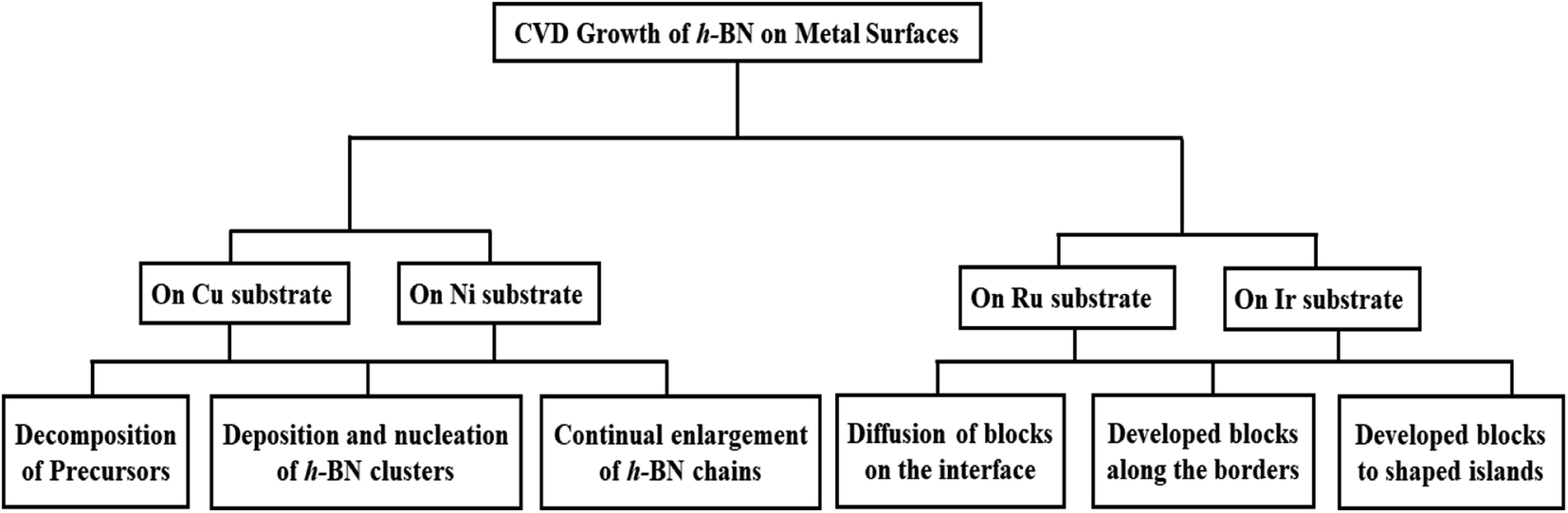
In addition, computer simulations and theoretical calculations can provide an extremely important means of understanding the growth mechanisms of 2D material synthesis.175–178 For example, recent first-principles calculations showed that anisotropic edge energies are important to the evolution of h-BN island morphology.179–184 The mechanisms of chemical reaction, crystal-forming pathways from the precursors and the prediction of growth morphologies have been revealed by the Reactive Force Field (ReaxFF) method.161,185 Moreover, first-principles calculations combined with a kinetic Monte Carlo (kMC) approach, have been used to forecast the morphology of island development as a function of flux and stoichiometry of precursors. Simple thermodynamic and kinetic analyses based on experimental findings can also help to understand growth mechanisms.177,178,186 All of these investigations have been done to learn more about how h-BN grows on metal surfaces. In this study, we will review the present state of research by the CVD technique in this field. We begin with the growth of h-BN, using CVD, on the most significant Cu substrate. Following that, investigations on additional surfaces, such as Ni and Ir/Ru, are discussed briefly. A schematic overview of the main topic discussed in this review is shown in Fig. 1. Finally, we provide a prognosis along with a concise summary.
 | ||
| Fig. 1 An overview of the CVD growth process covered in this manuscript. | ||
2. h-BN growth on the Cu substrate
Due to the widespread availability, cheap price, and ease of processing to transfer onto different substrates, polycrystalline Cu foils have been extensively utilized for the CVD development of h-BN.119,144,148,150,152,155,168,174,187–194 Despite significant success in producing h-BN on Cu and a variety of metal catalysts,119,144–150,152,153,155,168,169,187,194–202 the majority of attention has been on pre-treatment of the surface of the catalyst and adjusting the conditions of the precursors and/or exposure. Further advancement, such as controlling layer thickness, grain size, and layer number, necessitates a more complete knowledge, particularly of the basic interactions between B and N with the catalyst. The development of h-BN on Cu has been shown to be a surface-mediated mechanism.152,203 On the other hand, kidambi et al.194 demonstrated that h-BN grows isothermally on Cu when exposed to borazine at a high temperature, which is not just a result of surface-mediated growth. It is confirmed that B was incorporated into the majority of the catalyst by the expansion of the Cu lattice during high-temperature borazine exposure and the precipitation of elemental B from Cu after cooling. On the basis of this, they propose that B is taken up in the Cu catalyst, but N is not, showing that the catalyst as a whole has element-specific feeding mechanisms. However, additional knowledge about the growth process is largely based on investigations of other standard precursors without verification. The general growth strategy for h-BN consists of three phases:152,153,204–206 (i) precursors (borazane, borazine, etc.) decomposition, (ii) deposition and nucleation of h-BN clusters from the B and N-containing species, and (iii) continual enlargement of h-BN chains from these clusters and attachment to form a large film. All of these steps have recently been theoretically investigated, yielding significant new insights.21–24,28,30,31,34,207–2092.1 Decomposition of precursors
Various precursors, including ammonia borane (BNH6) or borazane, borane (BH3), borazine (B3H6N3), B-trichloroborazine (ClBNH)3, and diborane were thermally decomposed on catalytic metal surfaces to produce single and few-layer h-BN sheets.148,153,210–224 The diverse precursors used in the CVD process to synthesize h-BN are summarized in a recent review.174 Although borazine is isoelectronic with benzene, it is dangerous and decomposes rapidly, even at ambient temperatures. It is not an excellent choice due to its volatility. Borazine can pyrolyze and dehydrogenate to produce h-BN films, however partial dehydrogenation is more typical, leading to oligomeric BN molecules and irregular h-BN GBs.143,146,148,149,153,168,170,225–227 A recent work also supports this partial dehydrogenation of borazine (up to 880 K) and precedes the formation of h-BN. However, at elevated temperatures (>1000 K), a complete dehydrogenation of borazine may occur and an extra structure coexists with h-BN. Both are extremely reliant on the growth circumstances, but at sufficiently high temperatures, they invariably transition into a completely h-BN covered substrate, demonstrating that the latter is the thermodynamically more stable structure.228 B-trichloroborazine, a borazine derivative, has also been utilized to grow h-BN through the CVD technique.159,229 The production of HCl gas, when exposed to moist air, is a major disadvantage of this precursor, as it is erosive to CVD components and equipment. At normal temperatures, highly pure ammonia-borane exhibits no degradation after two months.230 When ammonia-borane is heated, hydrogen and volatile B- and N-containing compounds are formed, allowing h-BN to develop; the three compounds produced are monomeric aminoborane (H2N = BH2), borazine, and minor quantities of diborane.231,232 However, relying on the growth temperatures,233 substrate roughness,187,203 substrate structure,234 growth substrate position relative to the precursor source,155,233,235 and precursor flow, the formation of h-BN from ammonia-borane in the presence of H2 produces varying outcomes.142,152 Despite this, there is limited mechanistic information on the CVD development of h-BN from ammonia-borane, although one study shows that ammonia-borane-derived compounds on Cu are catalyzed near the surface.152In CVD growth, it is generally expected that the decomposition of precursor molecules should occur at the surface of the catalytic substrate. Borazine is produced and adsorbed on the catalytic substrate for precursors such as ammonia borane, B2H6/B10H14, and NH3. By dehydrogenation, borazine decomposes into B and N and produces monomers of B and N, or BN dimers, when it comes into contact with a metal substrate.182 The two most common lattice systems for metals are cubic and hexagonal close-packed (hcp). Face-centered cubic (fcc) (111) and hcp (0001) are two facets that are commonly employed in the CVD development of h-BN. B and N atoms can occupy three probable high symmetry sites on these surfaces: top (t), hcp (h), and fcc (f), as depicted in Fig. 2a–c.180 The binary composition of BN on metal surfaces allows for six different configurations: BhNf, BfNt, BtNh, BfNh, BhNt, and BtNf. These topologies are divided into two series, each having two local minima aligned in opposite directions. The difference in energy between two local minima is fairly small. The energy differences between BfNt and BhNt are just 9.2 meV (ref. 144) and 40 meV, respectively per unit cell on Ni (111) and Ru (0001), for example, and these differences are independent of cluster size.146 It is difficult to conceive that such minor changes in formation energy could confine h-BN domains in a well-aligned orientation, particularly when BN clusters are small. In this regard, Liu et al.182 used density functional theory (DFT) computations to investigate the formation energy and stabilization of BN structures of various geometries on Cu (111). They found that both B and N monomers prefer to be placed at each of the fcc positions on the Cu (111) substrate. On the other hand, the BN dimer seems to favor a BhcpNfcc structure, as shown in Fig. 2d.182 The formation energies of B and N monomers are 5.25 and 0.92 eV, correspondingly; however, the formation energy of a BN dimer is 3.08 eV, that is, lower than the total formation energies of two distinct B and N monomers. According to this evidence, the stability of a BN dimer is better than that of two B and N monomers. Moreover, the bond distance of the supported B–N dimer is 1.33 Å, which is smaller than that of the distance (1.45 Å) of a stand-alone h-BN film. To clearly understand the early stages of h-BN construction, the formation energy of h-BN domains with increasing population of atoms on the Cu (111) surface was measured.134,182 Although earlier works134,182 reveal that the B–N dimer is more energetically favorable than the pair of B and N monomers, the monomer and dimer formation energies are referenced to the energy of the metallic substrate. Moreover, the chemical potential of freestanding monolayer h-BN as well as the B and N in the reactor, the exact adsorbed species sourced from the feedstock were not taken into account in those works, indicating the absence of specific kinetics. There seems to be a shortage of information on the chemistry of the precursors.
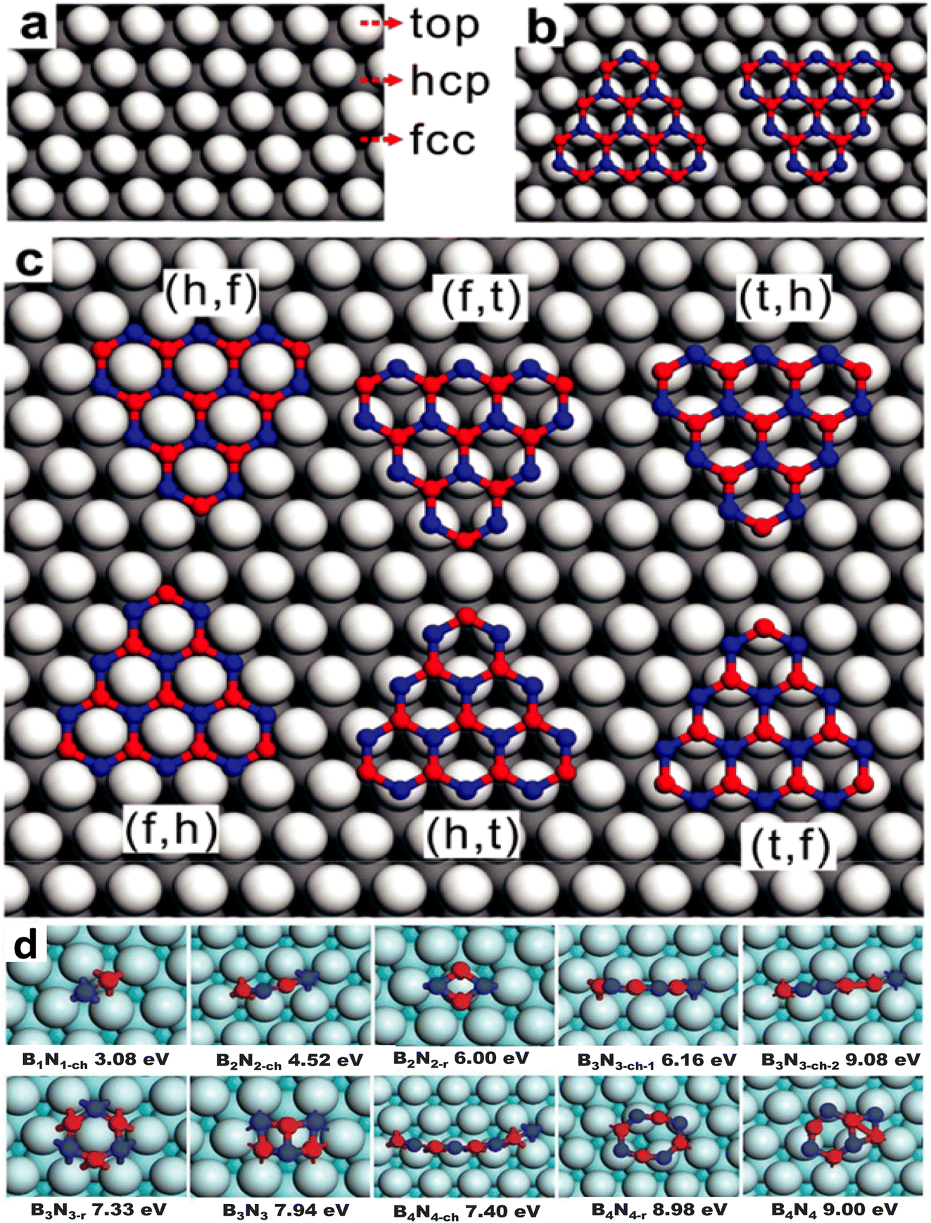 | ||
| Fig. 2 Atomistic model and formation energies of BN clusters on Cu with different lattice systems. (a) Three high symmetric points in face centered cubic (fcc) facet for the adsorption of B and N, (b) B and N-terminated triangular BN cluster alignments with identical adsorption sites (i.e., B at the hcp and N at the top position), and (c) adsorption sites of B and N are identified by their first letters in six potential configurations.180 (d) Formation energies of BnNn chains, rings, and sp2 networks on the Cu (111) surface.182 | ||
2.2 h-BN clusters on the Cu surface
It is vital to evaluate the possible BN species shape and evolution dynamics on the surface before proceeding to the nucleation step. Although BxNy is likely to be present on Cu surfaces, as mentioned in the previous section, the key parameters governing the BN cluster alignments are still unknown. However, the mechanism controlling the BN cluster orientations during initial growth offers techniques for building a high-quality h-BN film. It is possible to eliminate GBs by controlling the orientation of BN clusters on an appropriate metal surface. For example, the fcc Rh (111) metal surface was proposed to control the BN cluster and successfully used to create a single domain monolayer of h-BN.236 Zhao et al.180 checked the stabilities of various BN clusters on diverse metal catalysts such as Ni, Ag, Cu, Au, Pt, Ir, Pd, Rh, Co, and Ru with the two different facets, fcc (111) and hcp (0001). They identified that among the six topologies adopting the high symmetry sites, BhNt and BfNt are two local minima in almost all topologies, and the most energy-stable global minimum is found for the BhNt cluster, except in certain cases (for instance, the most energy-stable N-terminated BN clusters are found for BhNf on Cu (111)). Apart from that, the deviation in energy among BhNt and BfNt is just a few hundred meV, as depicted in Fig. 3c and d.180 The tiny difference in formation energy between the two local minima is consistent with other theoretical investigations.146 With the simultaneous creation of two local minima or a 60° rotation (or multiples of 60°) from the energetically-favored configurations, a global anti-parallel arrangement of BN clusters can be achieved on the identical metal terrace. High-resolution scanning tunneling microscopy (STM) images, on the other hand, revealed that nearly no BN clusters are positioned inversely (anti-parallel) on the same Ru terrace (0001).146 As a result, BN clusters must adopt a low energy shape, which will be conserved during future growth. It can be argued from these theoretical calculations that BN clusters prefer the lowest-energy conformation during early formation, and this conformation is largely conserved in forthcoming development.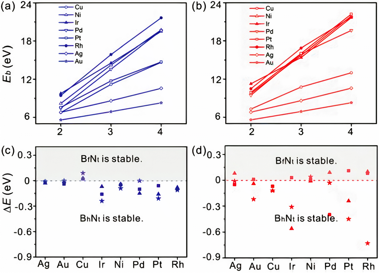 | ||
| Fig. 3 Binding energies as a function of BN clusters terminated with (a) N and (b) B atoms. The difference in formation energy between BhNt and BfNt of (c) N and (d) B terminated BN clusters. Squares, stars, and triangles represent the cluster size of 2, 3, and 4, respectively.180 | ||
It is widely believed that during the early stages of BN cluster development, edge atoms contribute a considerable proportion of the cluster. BN clusters are parallel on the fcc (111) interface, whereas they are anti-parallel on adjacent terraces and parallel on the same terrace on the hcp (0001) surface. As well as the underlying metal substrates' stacking arrangements, the alignment is also determined by the strong bond among the edge atoms and the substrates. Prior investigations also demonstrated that graphene edge atoms interact strongly with the underlying substrates.237,238 The binding energies (Eb) of distinct BN clusters can be used to intuitively investigate the impact of such an interaction. If this interaction is important for attaching BN clusters, Eb must progressively grow as the size of domain increases. The calculated Eb of the BN clusters on Cu (111) revealed that the Eb is very high and increases approximately linearly with increasing BN cluster size (Fig. 3a and b), regardless of whether they are terminated with N or B atoms. This finding verifies that the edge atom's interaction with the underlying substrate is the key factor in BN cluster docking. Furthermore, it is revealed that zigzag edges containing atoms with dangling bonds are the most stable BN cluster on metal substrates.179 If this is true, rotating the BN cluster will be more challenging because of strong contacts and increased charge transfer among the underlying metal atoms and the edge atoms.
Song et al. demonstrated by both experiment and DFT calculations that the crystallographic orientations of Cu substrates and the orientations of as-grown h-BN monolayers are closely related, with Cu (111) serving as the finest substrate for the formation of single-crystalline monolayers and aligned h-BN domains. However, opposing alignments of triangular BN have recently been found on Cu (111).239 According to the symmetry analysis, fcc (111) is a preferable choice for producing high-quality h-BN. Besides, experimental study revealed that large-area single-crystal monolayer h-BN can be grown on other orientations such as Cu (001) and vicinal Cu (110), the low symmetry of which eliminates twinning. However, which one is superior, given the abundance of possible catalysts in the fcc form? BhNt and BfNt are the local minima for BN clusters on most metal surfaces. A bigger difference between their formation energies is preferable to avoid the production of two local minima at the same time. The calculated energy difference between BN clusters on fcc (111) is limited to a range of 0–200 meV for N-terminated clusters, whereas it is much greater for B-terminated clusters. After complete relaxation, dome-like geometries emerge, producing larger position deviations from the initial ones, which may explain the substantially higher distribution seen in B-terminated clusters.
2.3 Nucleation of h-BN
Although the actual mechanism of hexagonal pattern generation and nucleation process is unknown, the following is one possible explanation. Aminoborane (BH2NH2) and borazine (B3H6N3) molecules break down into BN radicals at temperatures over 1050 °C and spread along the Cu surface as BN radicals.203 Surface mobility of free BN radicals is increased due to the decreased kinetic diffusion barrier provided by the smooth Cu surface. As a result, they can have larger diffusion lengths and can easily move ahead active borders. Earlier experiments have shown that electropolishing creates a smooth surface that increases the amount of oxygen on the Cu surface. The enhanced oxidation upon the Cu surface promotes the breakdown of the precursor gas and speeds up the dehydrogenation process around the domain edges.240 Lattice integration, like edge attachment, requires dehydrogenation at the domain boundaries, reducing the edge-connecting restriction. Due to the greater Gibbs free energy restriction and higher interface diffusion, nucleation is restricted, resulting in larger domains of h-BN. Furthermore, BN radicals can link for both the N and B terminated boundary, resulting in hexagonal-formed domains, because the energy barrier for edge-attachment reduces as the amount of surface oxygen increases. The roughness of an unprocessed Cu substrate, on the other hand, restricts surface diffusivity through trapping BN radicals owing to surface imperfections, constraining development, and only N-terminated corners are potentially advantageous owing to the absence of surface oxygen upon the Cu. As a result, a triangular-shaped h-BN domain is formed. The theoretical study by Liu et al.183 infers the energetically favored N-terminated zigzag edges over B-terminated ones, resulting in a triangular-shaped h-BN domain. And a hexagonal domain can only be formed if there are interchanging N and B terminated edges. Moreover, the growth of mono-orientated h-BN on a Cu substrate is largely influenced by the edge interfacial coupling. The edge-coupling-guided growth was confirmed by performing DFT calculations by Wang et al.154 The coupling of the h-BN nucleus (along the zigzag edges (Fig. 4a)) with the Cu 〈211〉 step edges produce a minimum formation energy at γ = 0° (Fig. 4b), indicating that γ = 0° is the preferred alignment between the h-BN films and Cu (110), where γ is the angle formed by the h-BN nucleus's zigzag direction and the Cu 〈211〉 direction (Fig. 4a). Hence, the nuclei of single-crystal h-BN domains can be formed by utilizing the interfacial coupling of the step edges of Cu 〈211〉 with the zigzag edges of h-BN.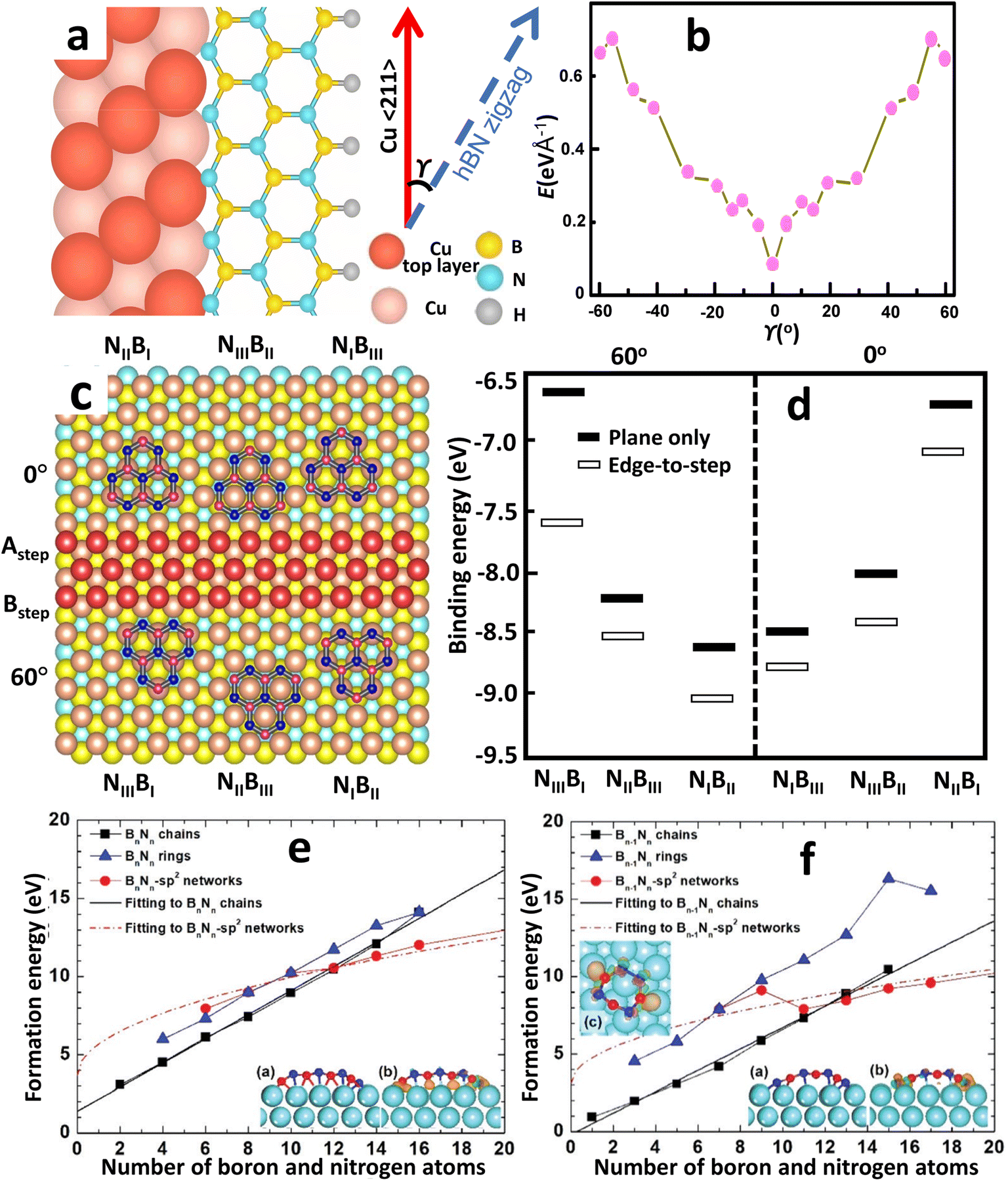 | ||
| Fig. 4 The process and dynamics of h-BN nucleation on a Cu substrate produced by CVD. (a) Schematic representations of the h-BN lattice on the Cu (110) atomic step. (b) Formation energies of different h-BN edges bonded to the Cu (110) substrate from DFT calculations.154 (c) Atomic arrangements with the lowest possible energy for six different atomic stacking configurations. (d) Calculated binding energies for the six configurations by DFT. (e and f) First-principles calculations of formation energies of Bn−1Nn and BnNn−1 chains, rings, and sp2 networks on Cu (111) surface versus the number of boron and nitrogen atoms in an h-BN cluster.182 | ||
DFT simulations were performed by Chen et al.241 for demonstrating the nucleation of epitaxial h-BN on Cu (111). A small and rigid B6N7 molecule has been considered as the probe seed to explain the preferred positioning of h-BN upon Cu (111). The effect of step edge and plane-to-plane epitaxy has been examined by calculating the binding energies of six typical atomic patterns, namely NIBIII, NIIIBII, NIIBI, NIBII, NIIBIII, and NIIIBI, where the first three configurations are defined as 0° orientation and the rest as 60° (inverted) orientation, as shown in Fig. 4c. The calculations on plane-to-plane epitaxy exhibit that clustering with N atoms upon surface of the first-layer Cu atoms (NIBIII (0°) and NIBII (60°)) has the minimum energy, whereas stacking with B atoms on the pinnacle of the first-layer Cu atoms (NIIBI (0°) and NIIIBI (60°)) are potentially unfavorable. The lowest-energy frameworks for 0° (NIBIII) and 60° (NIBII) configurations have an energy deviation of around 0.05 eV, which is far less than the thermal energy kBT at the growth temperature (approximately 0.1 eV), implying that such plane-to-plane registration is unlikely to attain mono-oriented development, in agreement with calculations.180 However, the presence of Cu step edges changes the binding energy of each arrangement in a minor but significant manner (Fig. 4d). The nearly degenerate (during plane-to-plane epitaxy) NIBIII (0°) and NIBII (60°) configurations are now separated by δE values of ∼0.23 eV. The Boltzmann selectivity factor eE/kBT is significantly amplified as this value increases in proportion to the docking length (just five to six hexagons in contact length improves the Boltzmann selectivity factor by more than 103). The mono-oriented growth appears to be ensured by such an energy difference.
The atomistic nucleation mechanism for 2D h-BN sheets on Cu surfaces has already been investigated by combining crystal growth theory with thorough atomistic simulations. In contrast to earlier beliefs that regularly generated BN triangles are thermodynamically specified, Zhang et al.179 show that the optimum form of BN islands is substantially influenced by the chemical state of the feedstock but generally varies from hexagon shapes or an experimental triangle. As a result, they looked at the non-equilibrium kinetics at the boundaries. Growth near the margins is marked by a very strong kinetic anisotropy, with a marked decrease in the formation of defects. It is possible to revise the kinetics of h-BN formation by regulating the chemical balance between B and N, which is a benefit. When N is abundant, the zigzag N-edge must surmount a significant nucleation obstacle and grow at the slowest rate of all edge directions, resulting in the production of N-terminated triangles mostly on the h-BN islands. Under B-rich conditions, BN geometries on Cu can grow towards shortened triangles as well as hexagons with extra B-terminated contour, similar to those observed in various studies, whereas h-BN islands on Ni can also be B-terminated triangles, implying that the boundary alignment for synthesizing h-BN triangles needs to be clarified.
The nucleation process in h-BN growth on a pristine Cu (111) can be understood more thoroughly from DFT analysis.182 Unlike carbon clusters, Liu et al.182 discovered that at a threshold size of 13, h-BN clusters on Cu supports can experience two different minimum-energy structural transitions. For cluster sizes below the critical limit, h-BN rings govern the minimum-energy structure because they are more stable on a Cu (111) surface than freestanding h-BN domains. Whenever the size of the cluster is fewer than 13 atoms, h-BN chains have the smallest formation energy and are much more stable than sp2 networks or h-BN rings, as demonstrated in Fig. 4e and f. When the cluster size exceeds 13, however, the h-BN chains are replaced by sp2 networks, which have the lowest formation energy. Based on the experimental circumstances of CVD growth, one-dimensional BnNn−1 (B-rich surroundings) or Bn−1Nn (N-rich) chains are generated initially, and then they transition to two-dimensional h-BN islands or sp2 networks; however, a BnNn chain does not transform to a two-dimensional sp2 network for an h-BN island. In h-BN islands, odd-membered rings seem extremely rare, as the most balanced structure is achieved by a mixture of hexagons and trapeziums at the edges, which preclude B–B as well as N–N bonding. Furthermore, trapeziums on a Cu (111) surface collapse whenever the four edges are linked to additional hexagons due to higher deformation energy, allowing planar nuclei to grow.
2.4 Lateral growth of h-BN islands
In order to obtain atomic data regarding the lateral expansion of h-BN islands, first one must determine which surface species are active and will be attached to an h-BN edge. Even though the formula is BxNy (x, y = 1, 2) to make the B–N bond, the dominant species are B–N dimers on the formation of h-BN island. During the growth process, one should also be aware of the structure of the h-BN edge. The growth conditions, such as pressure and temperature, may have an impact on two critical processes: hydrogen saturation and edge reconstruction. Using first-principles calculations, the energetics of the attachment process may be determined when both the edge structure and the surface species are known. A kinetic or thermodynamic (Wulff construction) analysis can then be used to predict the form of the h-BN island.242 On the other hand, a coarse-grained phase-field model may be utilized to represent the many growing geometries seen in the experiment.177,178,186,243,244Edge energies of the h-BN flakes are calculated to learn more about their morphologies. A number of theoretical investigations on the h-BN island edge structure and stability have been conducted.179,184,245 The zigzag (ZZ) and armchair (AC) edges, similar to graphene, are present on the h-BN sheet. To avoid inversion symmetry, the ZZ edge is divided into two distinct forms, the B-terminated (ZZ-B) and N-terminated (ZZ-N). The atomic structure of the crystal edge is difficult to determine experimentally. A crucial function for hydrogen in h-BN development is yet unknown, however it is thought to reduce active sites at the edges, boosting atomic diffusion down the edge and so altering the growth rate, as seen in graphene growth on Cu.246 In the CVD fabrication of h-BN sheets, BN precursors including ammonia borane (NH3–BH3),152,184 and borazine (N3B3H6)184,211,247 are commonly utilized. Experiments show that in such a situation, hydrogenation of the active BN edges is unavoidable.146,181,184,248 At elevated temperatures, the precursor (borazine) molecules undergo thermal decomposition, leading to the liberation of hydrogen and potential rupture of B–N bonds. This process facilitates the formation of highly reactive precursors, which exhibit strong adhesion to the surface and function as the fundamental building blocks for growth.248h-BN edges should be hydrogen saturated in an H-rich environment. The formation energies for different edges, such as ZZ-N, ZZ-N + B, ZZ-B, ZZ-B + N, AC, AC + N, and AC + B, without the H-termination are 10.87 eV nm−1, 19.30 eV nm−1, 12.96 eV nm−1, 9.87 eV nm−1, 7.57 eV nm−1, 13.14 eV nm−1, and 15.20 eV nm−1, respectively.184 The edge is found to be the most durable along the AC direction owing to the development of a BN bond, but the reconstructed edges, ZZ-B + N and ZZ-N, are more stable along with the zigzag ZZ directions.184 The formation energies of the same edges but terminated with H atom are −1.12 eV nm−1, 9.86 eV nm−1, 3.39 eV nm−1, 3.50 eV nm−1, 1.18 eV nm−1, 4.96 eV nm−1, and 11.60 eV nm−1, respectively.184 In the H-terminated edges, regardless of whether they are B-terminated, N-terminated, or armchair types, the pure (unreconstructed) edges are stable. In the H-terminated edges, regardless of whether they are B-terminated, N-terminated, or armchair types, the pure (unreconstructed) edges are stable.
On the Cu surface, the situation is different; theoretical calculations imply that h-BN triangular nanocrystals formed on the Cu surface must be terminated by nitrogen zigzag edges (ZZ-N).179 In contrast to earlier ideas that typically generated BN triangles are thermodynamically specified, the equilibrium form of BN islands is mostly determined by the chemical state of the feedstock, and it varies significantly from experimental triangle or hexagon forms.144,147,159,179,187,188,193,200,203,249,250 As a result, nonequilibrium kinetics near the edges need to be investigated. The nucleation sites of atomic arrays, which show significant kinetic anisotropy of growth, shape the BN islands into N-terminated triangles, which have since been discovered in experimental measurements,146,179,250 may be used to assess the growth rates for various edge orientations. Aside from edge hydrogenation, metal substrates may also play a role in stabilizing BN edges, as reported in graphene CVD development,184,237,251 which alters the equilibrium morphologies of BN islands and merits further extensive research in the future to imitate realistic scenarios in experiments.
For unconstructed edges, the edge energy for any given direction may be estimated by adding the energy of fundamental directions as follows:179,183,252
γ(χ) = |γ|![[thin space (1/6-em)]](https://www.rsc.org/images/entities/char_2009.gif) cos(χ + C) cos(χ + C) | (1) |
In contrast, the energies of conventional and regenerated edges on Cu, exhibit different results.179 Unlike graphene, the difference in chemical potential between B (μB) and N (μN) determines edge energies for h-BN, notably for the Klein (K) and ZZ edges, that have always been compositionally imbalanced. With the exception of the AC, all edges have a linear slope with μB, proportionate to the abundance of B atoms along the edge, as illustrated in Fig. 5a, b, and d. In N-rich circumstances, the ZZ-N is energetically preferred, while under B-rich situations, the ZZ-B is favored. At extremely high μN (i.e., low μB), additional N atoms may be added to rebuild the ZZ-B border into a more stable KB border. Similarly, at low μN, B attachment positively transforms the ZZ-N border into a KN border and the AC border into an AC-B border. Furthermore, since all of the edge atoms are securely attached to the fcc sites, there is no dimerization at the Klein edges on Cu. The thermodynamic Wulff construction on Cu substrate demonstrates that the equilibrium shape of h-BN is substantially influenced by μB, as shown in Fig. 5c and e. The BN form on Cu is a triangle with only ZZ-N edges in N-rich conditions. The structure develops into a nonagon with dominating ZZ-N edges and a minor piece of AC as B increases, and finally into a dodecagon with extra ZZ-B. The dodecagon shape is maintained as μB is increased, but the ZZ-N and AC edges are replaced with KN and AC-B edges, respectively. The form reverts to a nonagon encircled by the KN and AC-B edges at very high μB. These equilibrium morphologies on Cu usually deviate from the triangular143,152 and hexagonal119,203 h-BN islands that have been seen in experiments.179
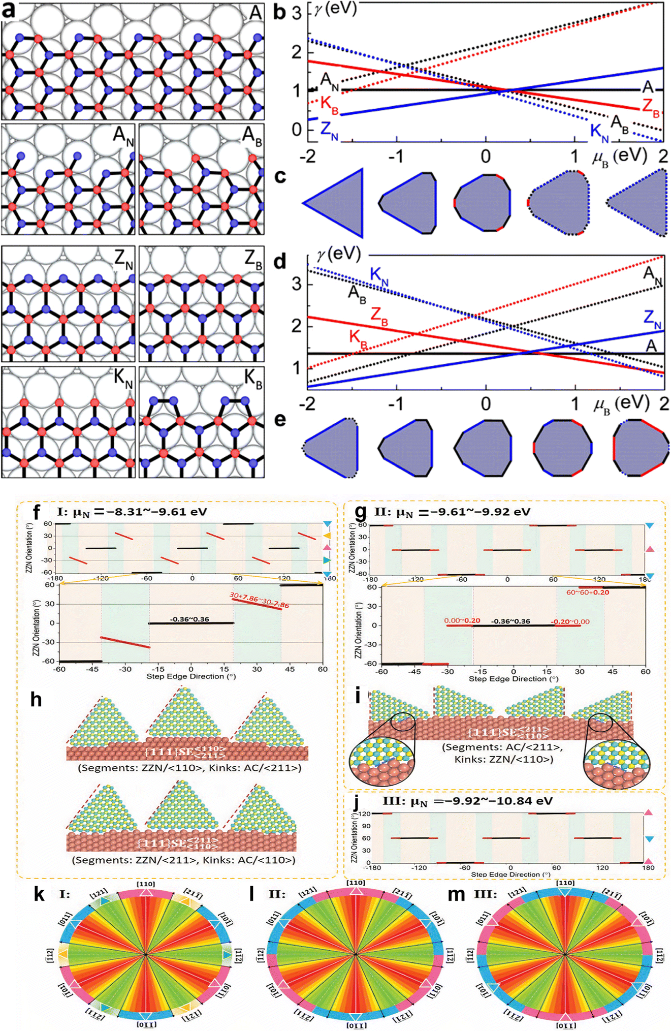 | ||
| Fig. 5 Various types of alignment, edges, and equilibrium structures of h-BN (a) reconstructed and conventional h-BN sheet edges on Ni, including armchair (A) and B- and N-terminated zigzag (ZB and ZN) edges. (b and d) h-BN edge energy on Ni (b) and Cu (d). (c and e) h-BN equilibrium forms on Ni (c) and Cu (e).179 (f–j) Alignment of h-BN along distinct Cu (111) serial high-index surface step edges at different chemical potential (μN). (k–m) h-BN islands' perimeter colors reflect orientation, with uniform colors indicating modest orientation changes and gradients indicating greater orientation changes.256 | ||
Zhang et al.255 demonstrated that the binding energies across h-BN edges and Cu step edges are significant for the high stability of the pure h-BN edge–step edge interfaces, and step edge type has no effect. The low edge formation energy of the pristine structure allows it to play a dominant role near a step edge for the AC edge, whilst the strong binding energies of the ZZ-N and ZZ-B edges allow for stable surfaces between pristine edges and Cu step edges, as revealed in Fig. 5f–m. The stability of interfaces between ZZ-N- and ZZ-B-serial edges, as well as step edges of Cu surfaces, is affected by the ambient environment due to their inequivalent binary composition. Furthermore, near the step edge of a Cu interface, the transition from reconstructed zigzag edges that are stable in a vacuum to the corresponding pristine structures is quite easy, confirming the importance of pristine zigzag edge–step edge interfaces in h-BN chemical vapor deposition formation on Cu substrates.
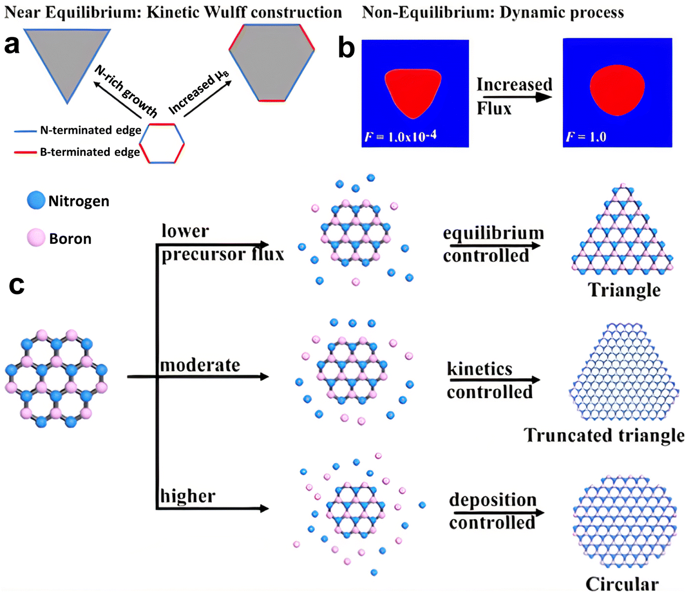
The thermodynamic balance postulated in the Wulff structure will not be disturbed at the slow growth limit. A kinetic expansion to the Wulff structure must be applied when the development process is out of equilibrium.257 The development of h-BN is influenced more by the dynamics at the borders than the border at equilibrium, according to previous research.179 The edge development velocity, which is anisotropic and dependent on the relative composition of the B and N, is determined by the energy barrier predicted by kinetic Wulff architecture. In B-rich environments, h-BN crystallization on Cu develops from triangles with N-terminated edges to shortened triangles having extra B-terminated edges. The dynamic Wulff construction hypothesis, as illustrated in Fig. 6a, convincingly describes the equilibrium shape of h-BN crystals as well as the progression from triangle to reduced triangle geometries at low precursor flux. Nevertheless, the projected designs dominated by kinetic Wulff building, such as triangles, truncated triangles, or hexagons, are only suitable for lower precursor flow, where consecutive insertion of atoms towards the kink points is preferred owing to the smaller energy threshold.179h-BN islands may experience a dynamic procedure including precursor breakdown, surface diffusion and, deposition when precursor flows are high enough to enable reactive regions, even with larger energy barriers to interact with inflow reactants quicker than edge structures relax. Therefore, the phase-field approach can be used to investigate the effect of precursor flux to qualitatively replicate these processes.258 Under a larger flux F, an evolution from triangular to circular shapes was discovered, with all other parameters remaining unchanged, according to phase-field simulation results (Fig. 6b). From this result, the authors presented a hypothesis of h-BN shape evolution as shown in Fig. 6c. At higher F, there is enough free reactant to promote h-BN growth, with inflow decomposition/deposition rates faster than absorption throughout every catalytic area along the growth line, resulting in isotropic circular shapes. The growth dynamics far from equilibrium are shown by phase-field modeling, where circular shapes are expected at greater reactant fluxes and are in agreement with experimental results.257
 | ||
| Fig. 6 (a) Kinetic Wulff model of h-BN evolution, exhibiting the preferred progression from triangle to truncated triangle with increasing boron chemical potential. (b) Nonequilibrium dynamics of h-BN development calculated from a phase field simulation, representing the triangle and circular shapes under low and high precursor flux, respectively. (c) Schematic representation of the progression of the h-BN pattern.257 | ||
Several parameters control the growth morphology and kinetics of h-BN. These include adatom deposition and desorption, substrate and edge diffusivities, precursor saturation, and anisotropies in edge energy, diffusivity, and mobility. To account for these factors, a multiscale phase-field model186 has been developed to foretell the morphology of h-BN growth by CVD. For h-BN growth on Cu (111), various alternative anisotropy combinations are taken into account, such as (i) just edge energy anisotropy, (ii) only edge mobility anisotropy, and (iii) both edge energy and mobility anisotropies. An island with only edge energy anisotropy is progressively transformed from being circular to being equilaterally triangular with rounded convex corners, with the long edge being the ZZ-N edge, which is consistent with the Wulff structures prediction. Due to the ZZ-N edge having much lower mobility than other edges, the island's shape is mostly triangular when just edge mobility anisotropy is considered, which is also compatible with the kinetic Wulff design. The island is developed into an equilateral triangle with sharper corners when both anisotropies are present, which is consistent with experimental findings,259 proving that the triangular h-BN islands under intermediate B:N ratio are the result of the interaction between edge energy and mobility anisotropies.
Defects are expected to be actively produced and healed during h-BN nonequilibrium development.174,260 Because of the undesirable homo-elemental binding forms (B–B bonds or N–N bonds), the Stone Wales defect, which is highly frequent in graphene, was expected to be energetically more favorable than the square octagonal pair (4|8) line imperfections in h-BN.261,262 Based on the tilt angle of the domain borders, DFT simulations reveal that both 5|7 (polar, B-rich, or N-rich) and 4|8 (unpolar) defects are energetically feasible in h-BN.263 Recent articles employed STM264 and high-resolution transmission electron microscopy (TEM)143,265 have detected both 4|8 and 5|7 type domain borders. Continuous h-BN films on Cu (111) with aligned 8|4 and 7|5 defects have also been reported.264 The domain borders of type 4|8 and 5|7 have been proposed as potential atomic configurations.264 4|8 type polar domain boundaries have been discovered among these configurations,265 while the others have yet to be empirically confirmed. Point defects are another type of disorder found in 2D materials. The point defects in h-BN can be either B/N-rich point defects or B/N vacancies because of the heteroatoms.266 Boron monovacancies are the most common defects in h-BN, according to Jin et al.267 During high-resolution TEM (HRTEM) imaging, boron monovacancies have been frequently produced with high-energy electron beams.188,267–269 The presence of boron vacancy defects is also observed through the utilization of annular dark-field-scanning transmission electron microscopy (ADF-STEM), as demonstrated by Wang et al.270 However, the formation of point defects in reduced types is typically induced by ion/electron irradiation of h-BN nanosheets.267,271,272 Alem et al. employed the reactive ion etching method to fabricate h-BN nanosheets featuring triangle-shaped boron vacancies of varying sizes.269 The predominant formation of B-typed vacancies with an N-terminated zigzag configuration has been observed in the atomic-layer h-BN. By aiming a high-energy electron beam on the boron monovacancy areas for several minutes, more B and N atoms can be pushed out from that layer, resulting in a triangular hole.188,267–269
The earlier theoretical research (and actual investigations) claimed that the formation energy of a single B vacancy (VB) is greater than that of a single N vacancy (VN), and hence nitrogen monovacancy formation should be preferred.273 Additionally, X-ray absorption near edge structure (XANES) spectroscopy in conjunction with ab initio calculations are used to find defects that are energetically advantageous.274 This research showed that the formation energy of the VB is greatly reduced by H passivation, stabilizing this defect and increasing the possibility that it would be found experimentally. Some experimental results may be contradicted by these theoretical suggestions. It's worth noting that the majority of these simulations were run under thermodynamic equilibrium settings, which aren't the same as the current experimental conditions. Because the vacancies were largely produced by high-energy charged electrons, the defect configurations could not be exactly the same as those predicted by thermodynamics. Although one of the previous investigations brought out the possibility of a paired vacancy generation during electron beam irradiation by considering the charge compensation of boron and nitrogen,275 no persistent divacancy (VBN) has been reported in h-BN. Due to the additional elimination of doubly coordinated boron atoms, the VBN should soon change to the multivacancy V3B+N, where three B and one N atoms are removed. However, Zobelli et al. demonstrated that B vacancies may migrate to generate more stable BN divacancies after being first thermally activated.276 At elevated temperatures, the divacancies may undergo additional activation. On the other hand, it is difficult to accurately define the intricacy of defects due to the non-equilibrium characteristics of material development and evolution processes.
The inversion symmetry of the binary h-BN lattice is broken, allowing for a far wider range of GB topologies to be discovered. Phase-field crystal (PFC) simulations have been extensively used to explore defect generation and the atomic structure of interfaces, GBs, and triple junctions.277 Taha et al.244 developed a phase-field crystal (PFC) model for binary 2D materials that can resolve crystalline microstructures while simultaneously addressing mesoscopic structural characteristics at diffusive time scales. The distinctive GB structure and collective domain dynamics of h-BN were studied using this PFC model, as shown in Fig. 7a–i.244 This study uncovers defect-mediated inversion domain development dynamics regulated by collectively atomic migration as well as defect core modification near grain borders and junctions, a mechanism linked to binary lattice inversion symmetry breaking. However, additional investigation is essential to fully comprehend the growth and repair processes of defects in h-BN on Cu substrates.
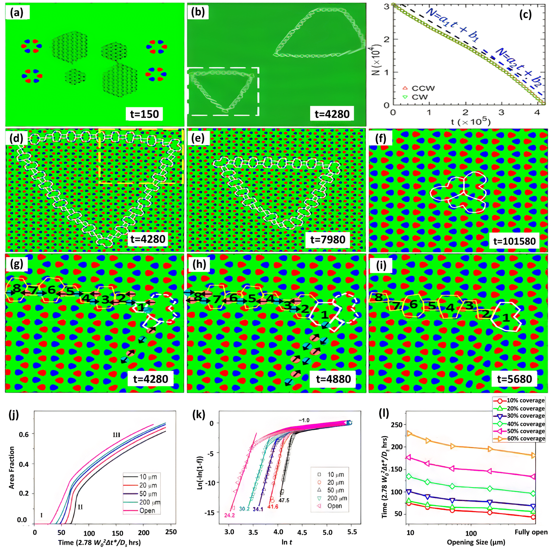 | ||
| Fig. 7 (a–i) Grain cohesion and inversion dynamics in the grain domain using phase field simulations.244 (j–l) Johnson–Mehl–Avrami–Kolmogorov (JMAK) investigation of the growth kinetics for varied opening sizes and substrate coverage development as a function of time.186 | ||
Another intriguing topic about h-BN growth at the island extension phase is whether it eventually leads to complete h-BN coverage on the Cu surface. The experimentally observed h-BN geometries have been explained in terms of the competition between deposition and edge diffusion186,278,279 using phase-field simulations.178,186,243,280,281 The phase-field model can be a useful tool for predicting h-BN nucleation and growth across the entire substrate. Using a phase-field model, the coverage of the Cu (111) surface with various sizes was recently examined.186 The entire growth kinetics may be evaluated using the Johnson–Mehl–Avrami–Kolmogorov (JMAK) formula, i.e. f = 1 − exp(−ktn); by linear modeling of ln(−ln(1 − f)) versus lnt (where k is a prefactor, f is the area fraction, and t is time) the fitted slope is the growth index n, as shown in Fig. 7j–l. The greatest h-BN island size develops with various entrance diameters are measured for different substrate coverages and growth timeframes. For a certain substrate opening size, the maximum island size grows with increasing time (or substrate coverage). For a certain growth period (or substrate coverage), the largest island size increases in proportion to the increase in substrate opening size, with the highest island size occurring at the fastest growth rate. This pattern is compatible with the previously mentioned island growth kinetics, where nucleation dominates the early phase of development (low growth time and coverage), while growth and coarsening dominate the later stages.
Even though the precise mechanism of the merging process and the modification of grain shape is still unclear, it is possible that the collisions of Cu atoms in the vapor with precursor molecules in the carrier gas, as well as with the Cu surface and edge of h-BN flakes, will have an impact. Theoretical investigations of the edge energy of h-BN have revealed that both the edge energies of ZN and ZB significantly depend on the chemical potential difference between B and N atoms, which is in turn dependent on the growth situation.183 Since the observed grain pattern cannot be predicted using the Wulff construction, the alteration in edge energies could not be the primary cause.183 Other elements, including the kinetic energy barrier, may also be responsible for variations in the concentration of copper vapor and are crucial to the development of h-BN. In fact, hexagonal defects with alternating ZN and ZB edges caused by electron irradiation have also been discovered before in the top layer of multilayer h-BN,282 suggesting that the alternating ZN and ZB edges are frequently seen in h-BN. The CVD growth also results in the production of interwoven polycrystalline aggregates in addition to isolated single-crystal domains. Yin et al. carried out a DFT calculations to investigate the adsorption of hydrogen atoms on the h-BN sheet with GBs in order to uncover the mechanism underlying the merging borders of these polycrystalline aggregates in h-BN.283 The hydrogen adsorption on the B atom is consistently found to be substantially more favorable than the N atom, which is in excellent agreement with other calculations.284–286 The adsorption energy typically rises as the adsorption site gets nearer to the GB and reaches a maximum at the intermediate neighborhood of the GBs. This outcome unequivocally demonstrates that the GB is more active after hydrogen etching. The B atom is chemically bound to the hydrogen adsorbed at the GBs, which causes the boron to be lifted out of the h-BN plane. Thus, the bonds connected to the boron that has been hydrogen-adsorbed locally break, and the nearby N atoms become into radical sites for more hydrogen adsorption. Particularly for those homo elemental bonds, the entire H chemisorption along the GBs make them structurally vulnerable to additional hydrogen attack. As a result, a structural disruption will occur mostly along the GB. In addition to the GB, the edges also show chemical activity that is comparable to hydrogen adsorption and offer additional locations to maintain the hydrogen etching.
3. Synthesis of h-BN on other metal substrates
Despite the fact that Cu is presently the most attractive substrate material for the CVD development of h-BN, h-BN has already been grown on a number of surfaces.287 Because Ni has been extensively employed in the CVD development of carbon compounds in the past, it is a favored choice among them. Some transition metals with large lattice constants have also been employed to produce h-BN, in addition to substrates like Cu and Ni with tiny lattice mismatches. The significant lattice distortion between h-BN and many large transition metals may form the non-commensurate corrugated nanomesh structures.288–292 The Moiré symmetry caused by the substrate's lattice mismatch with h-BN may be exploited to build a periodic nanoparticle crystalline structure with a variety of applications. Mechanisms of h-BN development have also been examined on substrates other than Cu, and this will be briefly discussed below.3.1 h-BN growth on Ni substrate
Besides Cu, Ni is one of the metal surfaces that has been investigated extensively for producing a pristine h-BN monolayer. Because of their potential to catalyze, Ni substrates can be used to make well-crystallized mono-, few-, and multilayer h-BN.144,293,294 Following exposure to B and N precursors at high-temperature, large areas of superior quality multilayer BN films can be formed on polycrystalline Ni substrates if a slow cooling rate is used. The ability of Ni to solubilize B and N at high temperatures allows for this procedure. At high temperatures, B and N diffuse into Ni films, then segregate at the surface during cooling, allowing BN domains to nucleate and develop. By saturating the Ni substrate with nitrogen by NH3 exposure ahead of the growth process, this precipitation-driven growth during cooling may be regulated and confined to a monolayer.293,295 Besides, by forming an intermediate boron oxide phase and then reducing it with carbon on the interior surface of a Ni enclosure, the film thickness can be confined to one or two layers with a lateral domain size of up to 100 μm, limiting the diffusion of B and N atoms into the bulk.293,296 Furthermore, Ma et al.160 recently observed that uniform aligned h-BN islands are formed at the initial stage on the single-crystal Ni (111) substrate. Eventually, these islands merge together to form a continuous film with a single crystal structure. The findings from cross-sectional transmission electron microscopy (TEM) indicate the presence of a Ni23B6 interlayer that is generated during the cooling process between the single-crystal h-BN film and Ni substrate. This interlayer is formed through the precipitation of boron atoms that were previously dissolved.Despite the fact that previous studies on CVD synthesized large area few layered h-BN on polycrystalline Cu and Ni foils using ammonia borane or borazine precursors149,150,187 at ambient pressure is demonstrated to be surface mediated, the control of layer thickness from a few layers to ∼100 layers using diborane and ammonia precursors144 is explained as neither surface-limited nor by segregation, but rather dependent on the surface chemistry of Ni having both Ni–B and Ni–N species present. There has not been a clear explanation offered that unifies these contradictory experimental data. In actuality, a segregation mechanism may have been the primary factor in the multilayer development process. Also, most studies outside of ultra-high vacuum (UHV) CVD growth168,199,297–299 have not been able to figure out why h-BN growth doesn't stop at a single layer and how multilayer h-BN films are made.
Although the major development mechanism is different, Ni may be studied using the same theoretical tools as Cu, as presented by Khan et al.174 Because the Ni dz2 orbital is substantially hybridized with the B-pz and N-pz orbitals, h-BN is claimed to be strongly chemisorbed on Ni (111).168,300,301 On the Ni (111) surface, theoretical investigations have been carried out to determine the positions of B and N atoms.302 The stable h-BN structure is formed by B atoms occupying the hollow sites of fcc or hcp Ni (111) sites, with N atoms occupying on top of each Ni atom.300,302 For B atoms, the fcc location is somewhat more energetically favorable than the hcp hollow sites (the energy difference between the two sites is 9 ± 2 meV/B atom).302 Ni (111) has a lattice mismatch of only 0.4% with h-BN (lattice spacing of Ni (111) = 0.249 nm and h-BN = 0.250 nm), which promotes comparable epitaxial development of h-BN on this surface. Based on a low energy electron diffraction (LEED) intensity study, Gamou et al. provided the first quantitative structural characterization of the h-BN/Ni (111) interface in 1997.303 On Ni (111), the h-BN generates a comparable 1 × 1 single-layer with a BfccNtop registry. The h-BN film is regular overall, but the B and N atoms are not stacked at the same height owing to the dissimilar binding of the two samples and the lattice mismatch, resulting in an atomic-scale corrugation. Adsorption heights of 2.0 Å and 2.9 Å were calculated using DFT calculations for the epitaxial and non-epitaxial structures, respectively. The low growth temperature could explain the formation of non-epitaxial h-BN domains not seen in earlier investigations.304 Theoretical analysis suggested both a chemisorbed (energy lowest) and a physisorbed (local energy minimum) state for h-BN/Ni (111),305–307 which is comparable to the graphene/Ni (111) system.308 Grad et al. published the first theoretical analysis on h-BN/Ni(111) in 2003, which found the BfccNtop registry to be favourable.302 Since then, a succession of DFT studies have concentrated on this interface.300,305,306,309–317 However, although the optimal adsorption configuration is widely agreed upon, adsorption energies, distances, hybridization levels, and charge redistribution are all affected by the degree of theory employed. These studies conclude that h-BN on Ni (111) is a geometrically planar, chemisorbed, commensurate overlayer with a common BfccNtop registry that differs slightly in height between the B and N atoms.
Furthermore, DFT-based reactive molecular dynamics (rMD) simulations are able to accurately describe the nucleation and evolution of h-BN/Ni (111).185 According to this rMD simulation, the first stage in the synthesis of the h-BN is to decompose the B and N-containing precursors (e.g., diborane and ammonia)144,193 into elemental B and N, followed by adsorption on Ni. The B and N atoms were then randomly placed on the Ni substrate, forming BN dimers, trimers (e.g., BNB), and short chains (e.g., BNBN). Long linear and branched BN chains up to 10 atoms have formed as the number of deposited B and N atoms has increased, and the core atoms (B or N) of each Y junction resemble an sp2-type hybridization. From the reaction energetics standpoint, DFT calculations confirmed the linear–branch–ring mode h-BN formation on the Ni substrate. To quantitatively analyze the nucleation process and formation of h-BN on the Ni surface, a stoichiometric B–N pair was used by calculating the adsorption energy as:
| AE = (EBxNx* − ENi − xEBN)/x | (2) |
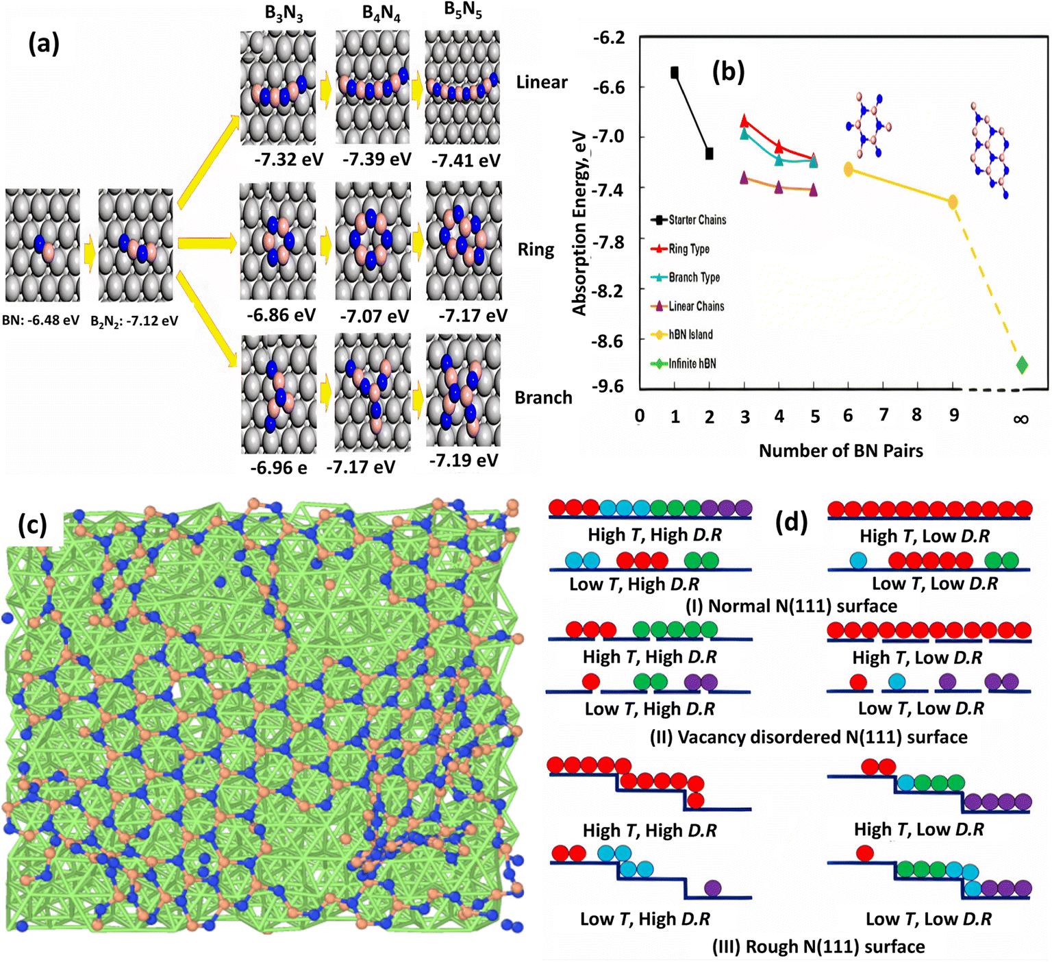 | ||
| Fig. 8 (a) Adsorption energies for optimized topologies of BN linear, ring, and branched configurations on Ni (111) surface. (b) Adsorption energy profile as a function of the number of BN pairs.185 (c) Surface structure at 1500 K and high deposition rate and (d) optimized growth conditions for h-BN growth on normal, vacancy-disordered, and step-terrace Ni (111) surfaces.206 | ||
The impacts of substrate architecture on the CVD development of h-BN have recently been investigated using rMD simulation.206 A low precursor deposition rate favors large single-domain h-BN growth on normal and vacancy-disordered Ni (111) substrates at high temperature (1500 K), but a greater deposition rate provides a single domain on rough (terrace and step structure) Ni (111) surfaces, as shown in Fig. 8c and d. For single-domain h-BN development, it is also discovered that the initial development rate of h-BN is higher on the rough surface and lower on the vacancy-disordered substrate. On a normal Ni surface, the creation of continuous h-BN islands is larger than on the other two substrates. Although a small vacancy concentration (1.25%) in the Ni (111) substrate has a minor influence on h-BN layer development, the rough surface has a distinct impact. The distribution and diffusion of B and N atoms in the substrate sublayers corroborated these conclusions, which were also supported by previous DFT calculations and experimental measurements.
3.2. Non-equilibrium growth on other metal surfaces
The Ru (0001) substrate has been studied extensively both experimentally and theoretically to grow the h-BN layer.319–321 Characteristic Moiré patterns are developed after the deposition of pure h-BN on Ru (0001) due to the production of a superstructure by the adsorbate and metal atom alignment.211 However, an unusual reaction-limited aggregation (RLA) growth kinetics has been revealed in h-BN on the Ru (0001) substrate. Usually, the growth kinetics of most 2D materials obeys the diffusion-limited aggregation (DLA) process, which exhibits a “fractal-to-compact” morphological change when growth temperature increases or deposition flux decreases. In situ scanning of h-BN development on a clean Ru (0001) surface and the Ru (0001) substrate containing subsurface Ar atoms revealed an atypical “compact-to-fractal” morphological shift with increasing growth temperature.322The aberrant growth mechanism of h-BN on Ru was investigated utilizing DFT calculations, with the BN dimers considered as the h-BN development blocks.323 Convolutions with “hills” (poor contact and energetically undesirable sites) and “pores” (intense contact and energetically desirable sites) emerge on the h-BN islands owing to the lattice mismatch among h-BN and Ru (0001).324 The reaction barrier (ER) for BN dimer attachment with produced h-BN islands on the clean Ru (0001) surface becomes 0.87 eV, whereas the diffusion barrier (ED) of BN dimers on the substrate becomes 0.60 eV, showing that the RLA methodology is followed during formation of h-BN islands on the clean Ru (0001) surface.325 Graphene development on Ru (0001)326 and Ir (111)327 substrates has been demonstrated to also follow the same RLA methodology. Due to the poor interaction of 2D material overlayers with metal surfaces, distances between them and the substrate surfaces are usually more than 3 Å.300,326,328 Different heights make it more challenging for growth blocks to connect to the island borders if they interact significantly with the surface. For h-BN growth on Ru (0001), it is claimed that h-BN growth blocks must jump this space in order to respond with the produced h-BN island edges (Fig. 9a), resulting in an increased interaction barrier. In weak interaction systems, such as h-BN on Cu, growth blocks interact with the surface weakly, enabling the hopping process to be easily overcome for the DLA mechanism to be active.300,329 As a result, the RLA process can only be observed in systems with strong interactions, including h-BN on Rh (111).330
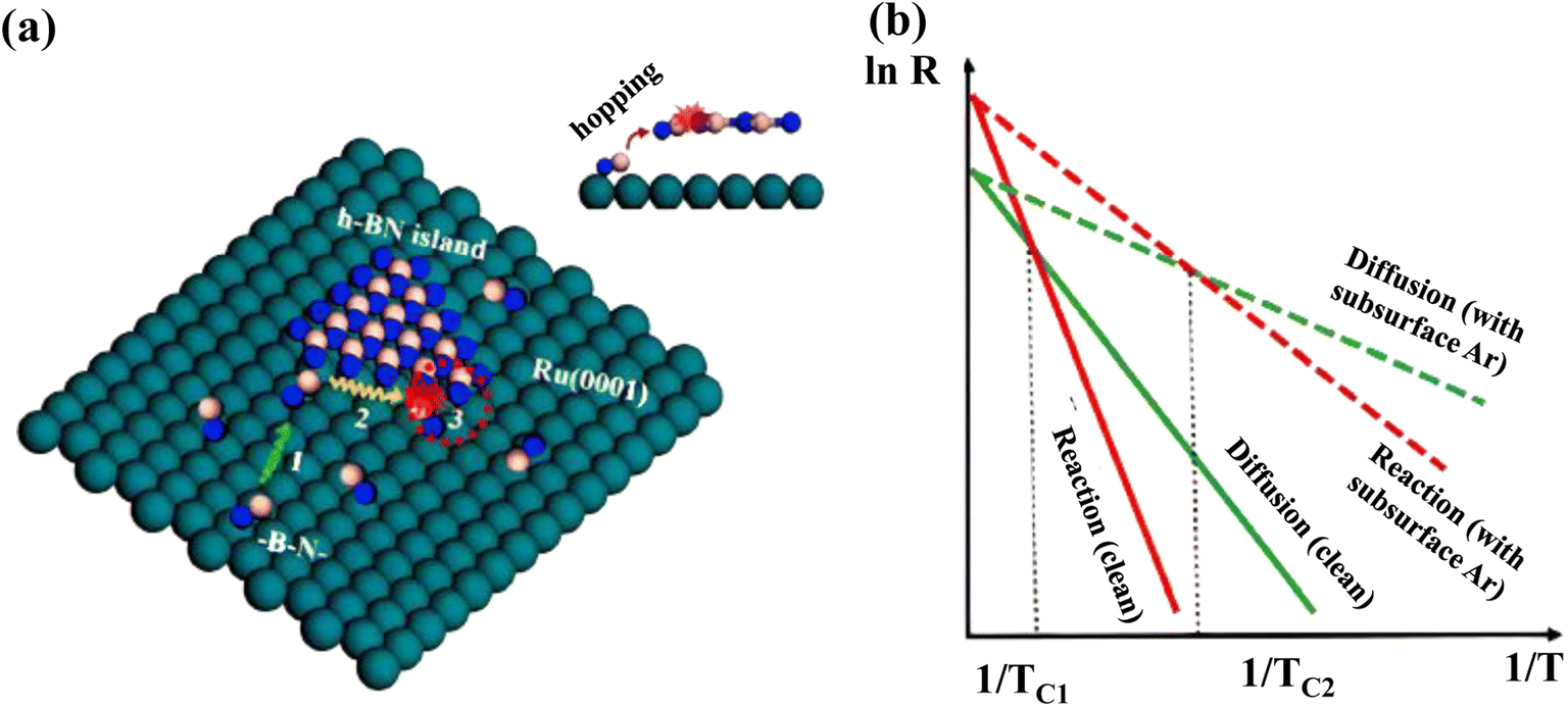 | ||
| Fig. 9 (a) Different phases of RLA process for h-BN development on Ru (0001): (1) growth blocks diffuse over the surface; (2) they relax around the margins of islands; and (3) they respond to the newly formed islands by doing things like hopping and attaching. A red dotted circle indicates step 3 in the inset's side perspective of the procedure. B, N, and Ru atoms are represented as pink, blue, and green balls, respectively. (b) Arrhenius plots for diffusing and reacting at the surface, with and without subsurface Ar atoms. The temperatures TC1 and TC2 denote the transition temperatures from a compact to a fractal morphology on the clean surface and the surface with subsurface Ar atoms, respectively.322 | ||
The surface development process is thought to still have three basic steps according to this discussion: (1) diffusion of developed blocks on the interface, (2) relaxing of developed blocks all along the borders of generated h-BN islands, and (3) reactivity of developed blocks to shaped islands, such as hopping and attachment. The final form of h-BN islands is resolved by the interplay between diffusion and reaction processes. When ER > ED, i.e., towards the RLA scenario, the reaction rate is inferior to the diffusion rate at low temperatures (Fig. 9b), and pre-arrived development blocks operate as shields to hinder arriving growth blocks from reaching island borders and causing yet another response, which is also known as the shielding effect.325 Compact h-BN islands emerge as a result of the “shielding effect”.325 The increased growth temperature aids in breaking down the reaction barrier, resulting in additional island edge locations available for interactions. The “shielding effect” is negligible in this situation, because pre-arrived development blocks don't have adequate time to relax around the borders, resulting in irregular h-BN islands forming at high temperatures. As a result, there must be a crossover point among the qualitative Arrhenius plots including both diffusion and reaction approaches, where the “compact-to-fractal” morphological conversion emerges and the temperature is specified as TC. In addition, the Wulff construction predicts the production of a hexagonal or triangular h-BN islands, but circular h-BN islands are relatively rare. The significant “shielding effect” at low temperatures and the fragile step limitation impact is thought to be responsible for the creation of spherical h-BN islands. The isotropic formation of h-BN islands is the result of a significant percentage of incoming development blocks (BN dimers) being localized along the established island boundaries.
The stepped morphology of the substrate employed in the CVD development of h-BN is mostly found to be a critical element in determining the most energetically stable shape of synthesized h-BN islands. The overall energy of the system is reduced by attaching h-BN edges to the Ir step edges during h-BN development. This is accomplished by rearranging Ir steps and forming trapezoids (rather than triangles). The relative orientation of h-BN island edges and Ir steps, as well as the chemical aspirations of B and N atoms throughout h-BN synthesis, determine the degree of Ir step rearrangement and the viability of the trapezoidal form.331
Large-scale continuous h-BN growth has also been accomplished on Ir substrate. The Moiré patterns are typically produced by the h-BN sheet grown on an Ir (111) surface as h-BN surface is well aligned with the substrate. Schulz et al. and Liu et al. examined the Moiré pattern of h-BN/Ir (111) in real space employing a combination of STM and DFT and found superstructure periodicities of 2.9 nm (ref. 332) and 3.2 nm,333 respectively. Both investigations also found considerably different geometric corrugation values, namely 0.4 Å (ref. 332) and 1.4 Å.333 Farwick Zum Hagen et al. recently published a study using multi-methods to characterize h-BN/Ir (111), namely by using X-ray standing wave (XSW), X-ray photoelectron spectroscopy (XPS), STM, LEED and DFT, which resolved the issue. A height variation of 1.55 Å was calculated between the strongly bound species (mean adsorption height 2.2 Å) and the weakly bound species (mean adsorption height 3.7 Å), using XSW and confirmed with DFT, categorizing h-BN/Ir (111) as a geometrically strongly corrugated structure.334 In addition, atomically detailed STM images revealed a Moiré regularity of 11.7 ± 0.3 times that of h-BN or 2.91 nm, which is only consistent with a 12-on-11 superstructure.334 As previously discussed,335 the geometry of h-BN and Ir (111) critically relies on the interplay between van der Waals (vdW) interactions and wave function hybridization, which makes them suitable test cases for vdW-treated DFT. In this regard, Seitsonen, Schulz, and Liljeroth recently obtained a mean corrugation value of 1.65 ± 0.23 Å from f(z) curves collected by nc-AFM at various places across the Moiré superstructure and utilized this value, in combination with the XSW findings stated above to calibrate vdW-treated DFT.335 Different approximations for the h-BN/Ir (111) system (such as vdW-DF2-C09, vdW-DF-rB86, vdW-DF2-rB86) produced good agreement with experimental results, whereas others (such as vdW-DF-optB88) failed, although appropriately describing comparable surfaces like graphene/Ir (111).335
Conclusions
Due to active studies from several experimental and theoretical groups over the last few years, our understanding of the mechanisms of h-BN development on metal substrates has greatly improved. The substrate plays a significant role in h-BN development. Some details about gas-phase processes, B and N source dehydrogenation, surface nucleation, and h-BN island growth have been revealed for the most interesting Cu substrate. In contrast to Cu, precipitation processes dominate h-BN development on the Ni surface. In the particular circumstance of h-BN growth, lattice mismatch is crucial, and the epitaxial pattern that results might influence growth kinetics.Despite the advances made thus far, there are still numerous unsolved difficulties in the realm of h-BN development. On one hand, the majority of theoretical investigations of h-BN development concentrate on a specific issue, and a unified atomic-scale growth process still remains elusive. CVD development of h-BN, on the contrary, is influenced by a variety of parameters, including substrate, temperature, feedstock, pressure, and so on. As a result, distinct development approaches may have completely dissimilar mechanisms, making theoretical research extremely challenging.
For instance, hydrogen has a significant impact on h-BN development, particularly on the Cu substrate. Its performance has already been proven in a laboratory setting. The necessary atomic processes, on the other hand, are almost entirely unknown. Nucleation on the Cu surface should be extremely difficult with BxNy on the surface. Second, controlling the number of surface layers is a crucial, but largely unexplored topic. Experimental evidence has been reported for both on-top and underlayer formation of multilayer h-BN, implying the possibility of several processes. Third, as nonlinear h-BN development on Ru and Ir substrates has shown, quantitative growth kinetics may be utilized to narrow the search for the growth process. Another intriguing finding is that h-BN formation on the Cu (100) surface appears attachment limited, but diffusion-limited on the Cu (111) surface. Such a perplexing outcome calls for a thorough theoretical investigation. Similar to graphene, it is important to explore whether BHx and NHx clusters, or even mixed BxNyHz clusters, may play a role in the development process of h-BN. Finally, with a greater understanding of growth mechanisms, the theoretical growth protocol design is progressively becoming realistic. Proposals to grow high-quality h-BN samples on an alloyed surface is one recent example.
Theoretical investigations of h-BN growth now rely primarily on first-principles computations and semi-empirical/empirical molecular dynamics simulations. Despite being widely used to investigate the development process of h-BN, the DFT approach has certain drawbacks. For instance, it can only mimic a system that generally has dimensions of less than a few nanometers and includes just a few hundred atoms. The DFT approach is often exclusively utilized for energy calculations and static structural relaxation. Recently, the dynamic development behavior of 2D materials has also been examined using ab initio molecular dynamics (AIMD). The whole simulation period, however, is often just a few tens of picoseconds. As compared to experiments, MD simulations are also still restricted in terms of tiny time and size scales. Evidently, a sizable comprehension gap still exists between MD models and actual experiments, preventing further research into these complicated systems. On the other hand, the lack of correlation between the model parameters and the experimentally controlled CVD processing parameters is a major barrier to the use of phase-field models for the computational synthesis of h-BN, and this is partly because of the disparity in the size scales of interest. The majority of current phase-field models only include the development of a small number of 2D islands (up to the micrometer scale), which scarcely adequately captures the influence of the macroscale CVD factors.
In prior investigations, additional methodologies including phenomenological analysis and kMC simulations have already been applied. Future kMC, reactive MD simulations, and phase-field modeling might provide important insights into the chemical development process of h-BN. The progress of many more advanced multiscale theoretical approaches seems likely to boost research in this sector greatly. The development of a trustworthy semi-empirical or empirical force field for Cu–B–N–H structures is likewise a pressing need. Advanced potential energy surface (PES) exploration techniques, including forward flux sampling, might become effective in determining the major nucleation route simultaneously and independently. The understanding of h-BN formation on metal substrates will continue to be deepened through the development of cutting-edge theoretical models, as well as experimental investigations.
Data availability
The data that support the findings of this study are available from the corresponding author upon reasonable request.Author contributions
M. S. I. conceived the work, A. A. M. M., M. U. S., and M. H. S. performed the data curation under the supervision of C. S. and J. P. All authors discussed and analyzed the data and interpretation and contributed during the writing of the manuscript.Conflicts of interest
The authors declare no competing financial or non-financial interests.Acknowledgements
This work is partially funded by the NV NASA EPSCoR RID Seed Grant (Grant Number 80NSSC19M0056).References
- S. H. Choi, S. J. Yun, Y. S. Won, C. S. Oh, S. M. Kim, K. K. Kim and Y. H. Lee, Nat. Commun., 2022, 13, 1484 CrossRef CAS PubMed.
- M. C. Lemme, D. Akinwande, C. Huyghebaert and C. Stampfer, Nat. Commun., 2022, 13, 1392 CrossRef CAS PubMed.
- O. Bubnova, Nat. Nanotechnol., 2021, 16, 1179 CrossRef CAS PubMed.
- K. V. Bets, N. Gupta and B. I. Yakobson, Nano Lett., 2019, 19, 2027–2031 CrossRef CAS PubMed.
- J. Dong, L. Zhang, X. Dai and F. Ding, Nat. Commun., 2020, 11(1), 1–8 CrossRef PubMed.
- K. S. Novoselov, A. K. Geim, S. V. Morozov, D. Jiang, Y. Zhang, S. V. Dubonos, I. v Grigorieva and A. A. Firsov, Science, 2004, 306, 666–669 CrossRef CAS PubMed.
- A. K. Geim and K. S. Novoselov, The Rise of Graphene Search PubMed.
- C. Zhang, S. Zhao, C. Jin, A. L. Koh, Y. Zhou, W. Xu, Q. Li, Q. Xiong, H. Peng and Z. Liu, Nat. Commun., 2015, 61(6), 1–8 Search PubMed.
- J. Li, M. Chen, A. Samad, H. Dong, A. Ray, J. Zhang, X. Jiang, U. Schwingenschlögl, J. Domke, C. Chen, Y. Han, T. Fritz, R. S. Ruoff, B. Tian and X. Zhang, Nat. Mater., 2022, 21(7), 740–747 CrossRef CAS PubMed.
- Z. Liu, L. H. G. Tizei, Y. Sato, Y. C. Lin, C. H. Yeh, P. W. Chiu, M. Terauchi, S. Iijima and K. Suenaga, Small, 2016, 12, 252–259 CrossRef CAS PubMed.
- Z. Han, M. Li, L. Li, F. Jiao, Z. Wei, D. Geng and W. Hu, Nanoscale, 2021, 13, 13174–13194 RSC.
- A. G. Bhuiyan, Y. Kamada, M. S. Islam, R. Syamoto, D. Ishimaru and A. Hashimoto, Results Phys., 2021, 20, 103714 CrossRef.
- M. S. Islam, I. Mia, S. Ahammed, C. Stampfl and J. Park, Sci. Rep., 2020, 10(1), 1–16 CrossRef PubMed.
- K. N. Anindya, M. S. Islam, A. Hashimoto and J. Park, Carbon, 2020, 168, 22–31 CrossRef CAS.
- M. S. Islam, K. N. Anindya, A. G. Bhuiyan and A. Hashimoto, Bull. Mater. Sci., 2019, 42, 1–5 CrossRef CAS.
- M. S. Islam, M. T. Rahaman, A. G. Bhuiyan and A. Hashimoto, J. Circuits Syst. Comput., 2015, 24(02), 1540002 CrossRef.
- M. S. Islam, A. G. Bhuiyan, S. Tanaka, T. Makino and A. Hashimoto, Appl. Phys. Lett., 2014, 105, 243103 CrossRef.
- M. S. Islam, K. Ushida, S. Tanaka, T. Makino and A. Hashimoto, Comput. Mater. Sci., 2014, 94, 35–43 CrossRef CAS.
- M. S. Islam, K. Ushida, S. Tanaka and A. Hashimoto, Comput. Mater. Sci., 2013, 79, 356–361 CrossRef CAS.
- S. R. Naqvi, G. S. Rao, W. Luo, R. Ahuja and T. Hussain, ChemPhysChem, 2017, 18, 513–518 CrossRef CAS PubMed.
- N. Kostoglou, K. Polychronopoulou and C. Rebholz, Vacuum, 2015, 112, 42–45 CrossRef CAS.
- X. Wang, M. Hossain, Z. Wei and L. Xie, Nanotechnology, 2018, 30, 034003 CrossRef PubMed.
- M. Cui, S. Ren, J. Chen, S. Liu, G. Zhang, H. Zhao, L. Wang and Q. Xue, Appl. Surf. Sci., 2017, 397, 77–86 CrossRef CAS.
- D. Gonzalez Ortiz, C. Pochat-Bohatier, J. Cambedouzou, M. Bechelany and P. Miele, Nanomaterials, 2018, 8, 716 CrossRef PubMed.
- B. Podgornik, T. Kosec, A. Kocijan and Č. Donik, Tribol. Int., 2015, 81, 267–275 CrossRef CAS.
- Z. Pawlak, T. Kaldonski, R. Pai, E. Bayraktar and A. Oloyede, Wear, 2009, 267, 1198–1202 CrossRef CAS.
- R. Laskowski, P. Blaha, T. Gallauner and K. Schwarz, Phys. Rev. Lett., 2007, 98, 106802 CrossRef PubMed.
- Y. J. Liu, B. Gao, D. Xu, H. M. Wang and J. X. Zhao, Phys. Lett. A, 2014, 378, 2989–2994 CrossRef CAS.
- R. Naresh Muthu, S. Rajashabala and R. Kannan, Renewable Energy, 2016, 85, 387–394 CrossRef CAS.
- B. Chettri, P. K. Patra, N. N. Hieu and D. P. Rai, Surf. Interfaces, 2021, 24, 101043 CrossRef CAS.
- G. Giovannetti, P. A. Khomyakov, G. Brocks, P. J. Kelly and J. van den Brink, Phys. Rev. B: Condens. Matter Mater. Phys., 2007, 76, 073103 CrossRef.
- B. Podgornik, F. Kafexhiu, T. Kosec, J. Jerina and M. Kalin, Wear, 2017, 388–389, 2–8 CrossRef CAS.
- F. Cataldo and S. Iglesias-Groth, J. Radioanal. Nucl. Chem., 2017, 313(1), 261–271 CrossRef CAS.
- A. S. Nazarov, V. N. Demin, E. D. Grayfer, A. I. Bulavchenko, A. T. Arymbaeva, H. J. Shin, J. Y. Choi and V. E. Fedorov, Chem. – Asian J., 2012, 7, 554–560 CrossRef CAS PubMed.
- H. Cho, S. Park, D. il Won, S. O. Kang, S. S. Pyo, D. I. Kim, S. M. Kim, H. C. Kim and M. J. Kim, Sci. Rep., 2015, 5(1), 1–10 Search PubMed.
- Y. Song, C. Zhang, B. Li, D. Jiang, G. Ding, H. Wang and X. Xie, Appl. Surf. Sci., 2014, 313, 647–653 CrossRef CAS.
- A. Pakdel, Y. Bando and D. Golberg, Chem. Soc. Rev., 2014, 43, 934–959 RSC.
- Z. J. Qi, S. J. Hong, J. A. Rodríguez-Manzo, N. J. Kybert, R. Gudibande, M. Drndic, Y. W. Park and A. T. C. Johnson, Small, 2015, 11, 1402–1408 CrossRef CAS PubMed.
- H. X. Jiang and J. Y. Lin, ECS J. Solid State Sci. Technol., 2017, 6, Q3012–Q3021 CrossRef CAS.
- S. K. Jang, J. Youn, Y. J. Song and S. Lee, Sci. Rep., 2016, 6(1), 1–9 CrossRef PubMed.
- M. S. Islam, K. N. Anindya, A. G. Bhuiyan, S. Tanaka, T. Makino and A. Hashimoto, Jpn. J. Appl. Phys., 2018, 57, 02CB04 CrossRef.
- M. S. Islam, K. Ushida, S. Tanaka, T. Makino and A. Hashimoto, Comput. Mater. Sci., 2014, 94, 225–233 CrossRef CAS.
- D. Gonzalez-Ortiz, C. Salameh, M. Bechelany and P. Miele, Mater. Today Adv., 2020, 8, 100107 CrossRef.
- S. Jia, W. Chen, J. Zhang, C. Y. Lin, H. Guo, G. Lu, K. Li, T. Zhai, Q. Ai and J. Lou, Mater. Today Nano, 2021, 16, 100135 CrossRef CAS.
- A. M. Satawara, G. A. Shaikh, S. K. Gupta and P. N. Gajjar, Mater. Today: Proc., 2021, 47, 529–532 CrossRef CAS.
- C. Jiao, T. Cai, H. Chen, X. Ruan, Y. Wang, P. Gong, H. Li, R. Atkin, F. Yang, H. Zhao, K. Nishimura, N. Jiang and J. Yu, Nanoscale Adv., 2023, 5, 711–724 RSC.
- S. Back and S. Siahrostami, Nanoscale Adv., 2019, 1, 132–139 RSC.
- M. S. Islam, A. H. Howlader, R. Zheng, C. Stampfl, J. Park and A. Hashimoto, ACS Omega, 2022, 7, 26591–26600 CrossRef CAS PubMed.
- S. Manzeli, D. Ovchinnikov, D. Pasquier, O. V. Yazyev and A. Kis, Nat. Rev. Mater., 2017, 2(8), 1–15 CrossRef.
- Q. H. Wang, K. Kalantar-Zadeh, A. Kis, J. N. Coleman and M. S. Strano, Nat. Nanotechnol., 2012, 7(11), 699–712 CrossRef CAS PubMed.
- Z. Hu, Z. Wu, C. Han, J. He, Z. Ni and W. Chen, Chem. Soc. Rev., 2018, 47, 3100–3128 RSC.
- A. A. Tedstone, D. J. Lewis and P. O'Brien, Chem. Mater., 2016, 28, 1965–1974 CrossRef CAS.
- Y. H. Wang, K. J. Huang and X. Wu, Biosens. Bioelectron., 2017, 97, 305–316 CrossRef CAS PubMed.
- A. Kuc, T. Heine and A. Kis, MRS Bull., 2015, 40, 577–584 CrossRef CAS.
- M. W. Iqbal, E. Elahi, A. Amin, G. Hussain and S. Aftab, Superlattices Microstruct., 2020, 137, 106350 CrossRef CAS.
- J. Ribeiro-Soares, R. M. Almeida, E. B. Barros, P. T. Araujo, M. S. Dresselhaus, L. G. Cançado and A. Jorio, Phys. Rev. B: Condens. Matter Mater. Phys., 2014, 90, 115438 CrossRef.
- X. Gu and R. Yang, Appl. Phys. Lett., 2014, 105, 131903 CrossRef.
- J. S. You, S. Fang, S. Y. Xu, E. Kaxiras and T. Low, Phys. Rev. B, 2018, 98, 121109 CrossRef CAS.
- H. Tian, M. L. Chin, S. Najmaei, Q. Guo, F. Xia, H. Wang and M. Dubey, Nano Res., 2016, 9(6), 1543–1560 CrossRef CAS.
- J. Choi, H. Zhang, H. Du and J. H. Choi, ACS Appl. Mater. Interfaces, 2016, 8, 8864–8869 CrossRef CAS PubMed.
- M. Gmitra and J. Fabian, Phys. Rev. B: Condens. Matter Mater. Phys., 2015, 92, 155403 CrossRef.
- L. Xiong, K. Wang, D. Li, X. Luo, J. Weng, Z. Liu and H. Zhang, FlatChem, 2020, 21, 100161 CrossRef CAS.
- Q. Wang, R. Shi, Y. Zhao, R. Huang, Z. Wang, A. Amini and C. Cheng, Nanoscale Adv., 2021, 3, 3430–3440 RSC.
- C. Wang, F. Yang and Y. Gao, Nanoscale Adv., 2020, 2, 4323–4340 RSC.
- A. Kagkoura, M. Pelaez-Fernandez, R. Arenal and N. Tagmatarchis, Nanoscale Adv., 2019, 1, 1489–1496 RSC.
- I. Z. Hlova, P. Singh, S. Z. Malynych, R. V. Gamernyk, O. Dolotko, V. K. Pecharsky, D. D. Johnson, R. Arroyave, A. K. Pathak and V. P. Balema, Nanoscale Adv., 2021, 3, 4065–4071 RSC.
- Q. Wang and D. Ohare, Chem. Rev., 2012, 112, 4124–4155 CrossRef CAS PubMed.
- K. H. Goh, T. T. Lim and Z. Dong, Water Res., 2008, 42, 1343–1368 CrossRef CAS PubMed.
- F. Li and X. Duan, Struct. Bonding, 2005, 119, 193–223 CrossRef.
- P. X. Zhi and Q. L. Guo, Chem. Mater., 2005, 17, 1055–1062 CrossRef.
- D. G. Evans and R. C. T. Slade, Struct. Bonding, 2005, 119, 1–87 CrossRef.
- A. Tyagi, M. Chandra Joshi, K. Agarwal, B. Balasubramaniam and R. K. Gupta, Nanoscale Adv., 2019, 1, 2400–2407 RSC.
- Z. Chen, H. Deng, M. Zhang, Z. Yang, D. Hu, Y. Wang and K. Yan, Nanoscale Adv., 2020, 2, 2099–2105 RSC.
- B. W. Xue, C. H. Zhang, Y. Z. Wang, W. W. Xie, N. W. Li and L. Yu, Nanoscale Adv., 2020, 2, 5555–5566 RSC.
- Y. Peng, Y. Li, Y. Ban, H. Jin, W. Jiao, X. Liu and W. Yang, Science, 2014, 346, 1356–1359 CrossRef CAS PubMed.
- C. Dey, T. Kundu, B. P. Biswal, A. Mallick and R. Banerjee, Acta Crystallogr., Sect. B: Struct. Sci., Cryst. Eng. Mater., 2013, 70, 3–10 CrossRef PubMed.
- R. Das, P. Pachfule, R. Banerjee and P. Poddar, Nanoscale, 2012, 4, 591–599 RSC.
- Q. Wang and D. Astruc, Chem. Rev., 2020, 120, 1438–1511 CrossRef CAS PubMed.
- N. Stock and S. Biswas, Chem. Rev., 2011, 112, 933–969 CrossRef PubMed.
- P. Yasaei, B. Kumar, T. Foroozan, C. Wang, M. Asadi, D. Tuschel, J. E. Indacochea, R. F. Klie and A. Salehi-Khojin, Adv. Mater., 2015, 27, 1887 CrossRef CAS PubMed.
- Y. Xu, Z. Shi, X. Shi, K. Zhang and H. Zhang, Nanoscale, 2019, 11, 14491–14527 RSC.
- Y. Du, C. Ouyang, S. Shi and M. Lei, J. Appl. Phys., 2010, 107, 093718 CrossRef.
- Y. Maruyama, S. Suzuki, K. Kobayashi and S. Tanuma, Physica B+C, 1981, 105, 99–102 CrossRef CAS.
- Y. Zhao, H. Wang, H. Huang, Q. Xiao, Y. Xu, Z. Guo, H. Xie, J. Shao, Z. Sun, W. Han, X. F. Yu, P. Li and P. K. Chu, Angew. Chem., Int. Ed., 2016, 55, 5003–5007 CrossRef CAS PubMed.
- G. Zhou, Z. Li, Y. Ge, H. Zhang and Z. Sun, Nanoscale Adv., 2020, 2, 1059–1065 RSC.
- T. Wang, X. Jin, J. Yang, J. Wu, Q. Yu, Z. Pan, H. Wu, J. Li, R. Su, J. Xu, K. Zhang, T. He and P. Zhou, Nanoscale Adv., 2019, 1, 195–202 RSC.
- Y. Miao, X. Wang, J. Sun and Z. Yan, Nanoscale Adv., 2021, 3, 1532–1550 RSC.
- P. Vogt, P. de Padova, C. Quaresima, J. Avila, E. Frantzeskakis, M. C. Asensio, A. Resta, B. Ealet and G. le Lay, Phys. Rev. Lett., 2012, 108, 155501 CrossRef PubMed.
- L. Li, S. Z. Lu, J. Pan, Z. Qin, Y. Q. Wang, Y. Wang, G. Y. Cao, S. Du and H. J. Gao, Adv. Mater., 2014, 26, 4820 CrossRef CAS PubMed.
- B. Feng, J. Zhang, Q. Zhong, W. Li, S. Li, H. Li, P. Cheng, S. Meng, L. Chen and K. Wu, Nat. Chem., 2016, 8(6), 563–568 CrossRef CAS PubMed.
- J. Meng, D. Wang, L. Cheng, M. Gao and X. Zhang, Nanotechnology, 2018, 30, 074003 CrossRef PubMed.
- M. R. H. Mojumder, M. S. Islam and J. Park, AIP Adv., 2021, 11, 015126 CrossRef CAS.
- J. D. Sarker, M. S. Islam, N. Ferdous, P. P. Sarker, A. G. Bhuiyan, T. Makino and A. Hashimoto, Jpn. J. Appl. Phys., 2019, 59, SCCC03 CrossRef.
- A. S. M. J. Islam, M. S. Islam, M. R. Islam, C. Stampfl and J. Park, Nanotechnology, 2021, 32, 435703 CrossRef CAS PubMed.
- A. S. M. J. Islam, M. S. Hasan, M. S. Islam and J. Park, Comput. Mater. Sci., 2021, 200, 110824 CrossRef CAS.
- M. R. Islam, M. S. Islam, A. F. Mitul, M. R. H. Mojumder, A. S. M. J. Islam, C. Stampfl and J. Park, Sci. Rep., 2021, 11(1), 1–14 CrossRef PubMed.
- M. S. Islam, I. Mia, A. S. M. J. Islam, C. Stampfl and J. Park, Sci. Rep., 2022, 12(1), 1–15 CrossRef PubMed.
- A. S. M. J. Islam, M. S. Islam, N. Ferdous, J. Park and A. Hashimoto, Phys. Chem. Chem. Phys., 2020, 22, 13592–13602 RSC.
- A. S. M. J. Islam, M. S. Islam, N. Ferdous, J. Park, A. G. Bhuiyan and A. Hashimoto, Nanotechnology, 2019, 30, 445707 CrossRef CAS PubMed.
- M. S. Islam, A. S. M. J. Islam, O. Mahamud, A. Saha, N. Ferdous, J. Park and A. Hashimoto, AIP Adv., 2020, 10, 15117 CrossRef CAS.
- A. S. M. Jannatul Islam, Md. Sherajul Islam, N. Zannat Mim, Md. Shahadat Akbar, M. Sayed Hasan, M. Rasidul Islam, C. Stampfl and J. Park, ACS Omega, 2022, 7, 4525–4537 CrossRef PubMed.
- M. S. Islam, S. Tanaka and A. Hashimoto, Carbon, 2014, 80, 146–154 CrossRef CAS.
- S. Ahammed, M. S. Islam, I. Mia and J. Park, Nanotechnology, 2020, 31, 505702 CrossRef CAS PubMed.
- M. S. Islam, M. Y. Zamil, M. R. H. Mojumder, C. Stampfl and J. Park, Sci. Rep., 2021, 11(1), 1–12 CrossRef PubMed.
- A. Arafat, M. S. Islam, N. Ferdous, A. S. M. J. Islam, M. M. H. Sarkar, C. Stampfl and J. Park, Sci. Rep., 2022, 12(1), 1–12 CrossRef PubMed.
- N. Ferdous, M. S. Islam, J. Biney, C. Stampfl and J. Park, Sci. Rep., 2022, 12(1), 1–13 CrossRef PubMed.
- A. S. M. J. Islam, M. S. Akbar, M. S. Islam and J. Park, ACS Omega, 2021, 6, 21861–21871 CrossRef CAS PubMed.
- A. H. Howlader, M. S. Islam and N. Ferdous, Optoelectron. Lett., 2021, 17, 454–458 CrossRef.
- M. S. Islam, M. R. H. Mojumder, N. Ferdous and J. Park, Mater. Today Commun., 2021, 26, 101718 CrossRef CAS.
- A. S. Rashid, M. S. Islam, N. Ferdous, K. N. Anindya, J. Park and A. Hashimoto, J. Comput. Electron., 2019, 18, 836–845 CrossRef CAS.
- N. Ferdous, M. S. Islam, J. Park and A. Hashimoto, AIP Adv., 2019, 9, 25120 CrossRef.
- M. Fahim-Al-Fattah, M. T. Rahman, M. S. Islam and A. G. Bhuiyan, Int. J. Nanosci., 2016, 15(03), 1640001 CrossRef CAS.
- A. H. Howlader, M. S. Islam, S. Tanaka, T. Makino and A. Hashimoto, Jpn. J. Appl. Phys., 2018, 57, 02CB08 CrossRef.
- M. R. Islam, M. S. Islam, N. Ferdous, K. N. Anindya and A. Hashimoto, J. Comput. Electron., 2019, 18, 407–414 CrossRef CAS.
- K. N. Anindya, M. S. Islam, J. Park, A. G. Bhuiyan and A. Hashimoto, Curr. Appl. Phys., 2020, 20, 572–581 CrossRef.
- M. S. Islam, A. H. Howlader, K. N. Anindya, R. Zheng, J. Park and A. Hashimoto, J. Appl. Phys., 2020, 128, 045108 CrossRef CAS.
- L. H. Li, J. Cervenka, K. Watanabe, T. Taniguchi and Y. Chen, ACS Nano, 2014, 8, 1457–1462 CrossRef CAS PubMed.
- A. Nagashima, N. Tejima, Y. Gamou, T. Kawai and C. Oshima, Phys. Rev. Lett., 1995, 75, 3918 CrossRef CAS PubMed.
- S. Chatterjee, Z. Luo, M. Acerce, D. M. Yates, A. T. C. Johnson and L. G. Sneddon, Chem. Mater., 2011, 23, 4414–4416 CrossRef CAS.
- H. Zhou, J. Zhu, Z. Liu, Z. Yan, X. Fan, J. Lin, G. Wang, Q. Yan, T. Yu, P. M. Ajayan and J. M. Tour, Nano Res., 7, 1232–1240 CrossRef CAS.
- R. Kumar, G. Rajasekaran and A. Parashar, Nanotechnology, 2016, 27, 085706 CrossRef PubMed.
- K. Watanabe, T. Taniguchi and H. Kanda, Nat. Mater., 2004, 3, 404–409 CrossRef CAS PubMed.
- D. Golberg, Y. Bando, Y. Huang, T. Terao, M. Mitome, C. Tang and C. Zhi, ACS Nano, 2010, 4, 2979–2993 CrossRef CAS PubMed.
- G. Lu, K. Yu, Z. Wen and J. Chen, Nanoscale, 2013, 5, 1353–1368 RSC.
- C. R. Dean, A. F. Young, I. Meric, C. Lee, L. Wang, S. Sorgenfrei, K. Watanabe, T. Taniguchi, P. Kim, K. L. Shepard and J. Hone, Nat. Nanotechnol., 2010, 5, 722–726 CrossRef CAS PubMed.
- R. v. Gorbachev, A. K. Geim, M. I. Katsnelson, K. S. Novoselov, T. Tudorovskiy, I. V. Grigorieva, A. H. MacDonald, S. V. Morozov, K. Watanabe, T. Taniguchi and L. A. Ponomarenko, Nat. Phys., 2012, 8, 896–901 Search PubMed.
- J. Yu, L. Qin, Y. Hao, S. Kuang, X. Bai, Y. M. Chong, W. Zhang and E. Wang, ACS Nano, 2010, 4, 414–422 CrossRef CAS PubMed.
- C. Zhi, Y. Bando, C. Tang, H. Kuwahara and D. Golberg, Adv. Mater., 2009, 21, 2889–2893 CrossRef CAS.
- K. Ahmed, R. Dahal, A. Weltz, J. Q. Lu, Y. Danon and I. B. Bhat, Appl. Phys. Lett., 2016, 109, 113501 CrossRef.
- A. Maity, T. C. Doan, J. Li, J. Y. Lin and H. X. Jiang, Appl. Phys. Lett., 2016, 109, 072101 CrossRef.
- K. Watanabe, T. Taniguchi, T. Niiyama, K. Miya, M. Taniguchi, K. Watanabe, T. Taniguchi, T. Niiyama, K. Miya and M. Taniguchi, Nat. Photonics, 2009, 3, 591–594 CrossRef CAS.
- H. X. Jiang and J. Y. Lin, Semicond. Sci. Technol., 2014, 29, 084003 CrossRef CAS.
- T. T. Tran, C. Zachreson, A. M. Berhane, K. Bray, R. G. Sandstrom, L. H. Li, T. Taniguchi, K. Watanabe, I. Aharonovich and M. Toth, Phys. Rev. Appl., 2016, 5, 034005 CrossRef.
- H. Liu, C. Y. You, J. Li, P. R. Galligan, J. You, Z. Liu, Y. Cai and Z. Luo, Nano Mater. Sci., 2021, 3, 291–312 CrossRef CAS.
- K. M. Taylor, Ind. Eng. Chem., 2002, 47, 2506–2509 CrossRef.
- J. D. Caldwell, A. v. Kretinin, Y. Chen, V. Giannini, M. M. Fogler, Y. Francescato, C. T. Ellis, J. G. Tischler, C. R. Woods, A. J. Giles, M. Hong, K. Watanabe, T. Taniguchi, S. A. Maier and K. S. Novoselov, Nat. Commun., 2014, 5, 1–9 Search PubMed.
- D. Paciĺ, J. C. Meyer, Ç. Girit and A. Zettl, Appl. Phys. Lett., 2008, 92, 133107 CrossRef.
- G. R. Bhimanapati, N. R. Glavin and J. A. Robinson, in Semiconductors and Semimetals, Academic Press Inc., 2016, vol. 95, pp. 101–147 Search PubMed.
- K. Zhang, Y. Feng, F. Wang, Z. Yang and J. Wang, J. Mater. Chem. C, 2017, 5, 11992–12022 RSC.
- S. Bernard and P. Miele, Mater. Today, 2014, 17, 443–450 CrossRef CAS.
- L. Li, Y. Zhang, R. Zhang, Z. Han, H. Dong, G. Yu, D. Geng and H. Y. Yang, Nanoscale, 2021, 13, 17310–17317 RSC.
- Y. Gao, W. Ren, T. Ma, Z. Liu, Y. Zhang, W. bin Liu, L. P. Ma, X. Ma and H. M. Cheng, ACS Nano, 2013, 7, 5199–5206 CrossRef CAS PubMed.
- A. L. Gibb, N. Alem, J. H. Chen, K. J. Erickson, J. Ciston, A. Gautam, M. Linck and A. Zettl, J. Am. Chem. Soc., 2013, 135, 6758–6761 CrossRef CAS PubMed.
- A. Ismach, H. Chou, D. A. Ferrer, Y. Wu, S. McDonnell, H. C. Floresca, A. Covacevich, C. Pope, R. Piner, M. J. Kim, R. M. Wallace, L. Colombo and R. S. Ruoff, ACS Nano, 2012, 6, 6378–6385 CrossRef CAS PubMed.
- G. Kim, A. R. Jang, H. Y. Jeong, Z. Lee, D. J. Kang and H. S. Shin, Nano Lett., 2013, 13, 1834–1839 CrossRef CAS PubMed.
- J. Lu, P. S. E. Yeo, Y. Zheng, H. Xu, C. K. Gan, M. B. Sullivan, A. H. Castro Neto and K. P. Loh, J. Am. Chem. Soc., 2013, 135, 2368–2373 CrossRef CAS PubMed.
- C. M. Orofeo, S. Suzuki, H. Kageshima and H. Hibino, Nano Res., 2013, 6(5), 335–347 CrossRef CAS.
- S. Roth, F. Matsui, T. Greber and J. Osterwalder, Nano Lett., 2013, 13, 2668–2675 CrossRef CAS PubMed.
- Y. Shi, C. Hamsen, X. Jia, K. K. Kim, A. Reina, M. Hofmann, A. L. Hsu, K. Zhang, H. Li, Z. Y. Juang, M. S. Dresselhaus, L. J. Li and J. Kong, Nano Lett., 2010, 10, 4134–4139 CrossRef CAS PubMed.
- L. Song, L. Ci, H. Lu, P. B. Sorokin, C. Jin, J. Ni, A. G. Kvashnin, D. G. Kvashnin, J. Lou, B. I. Yakobson and P. M. Ajayan, Nano Lett., 2010, 10, 3209–3215 CrossRef CAS PubMed.
- L. Li, Y. Zhang, R. Zhang, Z. Han, H. Dong, G. Yu, D. Geng and H. Y. Yang, Nanoscale, 2021, 13, 17310–17317 RSC.
- K. K. Kim, A. Hsu, X. Jia, S. M. Kim, Y. Shi, M. Hofmann, D. Nezich, J. F. Rodriguez-Nieva, M. Dresselhaus, T. Palacios and J. Kong, Nano Lett., 2012, 12, 161–166 CrossRef PubMed.
- P. Sutter, J. Lahiri, P. Albrecht and E. Sutter, ACS Nano, 2011, 5, 7303–7309 CrossRef CAS PubMed.
- L. Wang, X. Xu, L. Zhang, R. Qiao, M. Wu, Z. Wang, S. Zhang, J. Liang, Z. Zhang, Z. Zhang, W. Chen, X. Xie, J. Zong, Y. Shan, Y. Guo, M. Willinger, H. Wu, Q. Li, W. Wang, P. Gao, S. Wu, Y. Zhang, Y. Jiang, D. Yu, E. Wang, X. Bai, Z. J. Wang, F. Ding and K. Liu, Nature, 2019, 570, 91–95 CrossRef CAS PubMed.
- N. Guo, J. Wei, L. Fan, Y. Jia, D. Liang, H. Zhu, K. Wang and D. Wu, Nanotechnology, 2012, 23, 415605 CrossRef PubMed.
- A. Gibb, N. Alem and A. Zettl, Phys. Status Solidi B, 2013, 250, 2727–2731 CrossRef CAS.
- Z. Cheng, M. Xia, S. Liu, R. Hu, G. Liang and S. Zhang, Appl. Surf. Sci., 2019, 476, 1008–1015 CrossRef CAS.
- Y. Kobayashi, T. Nakamura, T. Akasaka, T. Makimoto and N. Matsumoto, J. Cryst. Growth, 2007, 298, 325–327 CrossRef CAS.
- W. Auwärter, H. U. Suter, H. Sachdev and T. Greber, Chem. Mater., 2003, 16, 343–345 CrossRef.
- K. Y. Ma, L. Zhang, S. Jin, Y. Wang, S. I. Yoon, H. Hwang, J. Oh, D. S. Jeong, M. Wang, S. Chatterjee, G. Kim, A. R. Jang, J. Yang, S. Ryu, H. Y. Jeong, R. S. Ruoff, M. Chhowalla, F. Ding and H. S. Shin, Nature, 2022, 606, 88–93 CrossRef CAS PubMed.
- S. Liu, J. Comer, A. C. T. van Duin, D. M. van Duin, B. Liu and J. H. Edgar, Nanoscale, 2019, 11, 5607–5616 RSC.
- C. Kowanda and M. O. Speidel, Scr. Mater., 2003, 48, 1073–1078 CrossRef CAS.
- Y. Kubota, K. Watanabe, O. Tsuda and T. Taniguchi, Science, 2007, 317, 932–934 CrossRef CAS PubMed.
- T. G. Senthamaraikannan, C. W. Yoon and D. H. Lim, Nanoscale Adv., 2023, 5, 2422–2426 RSC.
- J. D. Caldwell, I. Aharonovich, G. Cassabois, J. H. Edgar, B. Gil and D. N. Basov, Nat. Rev. Mater., 2019, 4(8), 552–567 CrossRef CAS.
- G. Zhao, A. Wang, W. He, Y. Xing and X. Xu, Adv. Mater. Interfaces, 2019, 6(7), 1900062 CrossRef CAS.
- S. Roy, X. Zhang, A. B. Puthirath, A. Meiyazhagan, S. Bhattacharyya, M. M. Rahman, G. Babu, S. Susarla, S. K. Saju, M. K. Tran, L. M. Sassi, M. A. S. R. Saadi, J. Lai, O. Sahin, S. M. Sajadi, B. Dharmarajan, D. Salpekar, N. Chakingal, A. Baburaj, X. Shuai, A. Adumbumkulath, K. A. Miller, J. M. Gayle, A. Ajnsztajn, T. Prasankumar, V. V. J. Harikrishnan, V. Ojha, H. Kannan, A. Z. Khater, Z. Zhu, S. A. Iyengar, P. A. da S. Autreto, E. F. Oliveira, G. Gao, A. G. Birdwell, M. R. Neupane, T. G. Ivanov, J. Taha-Tijerina, R. M. Yadav, S. Arepalli, R. Vajtai and P. M. Ajayan, Adv. Mater., 2021, 33, 2101589 CrossRef CAS PubMed.
- A. B. Preobrajenski, A. S. Vinogradov and N. Mårtensson, Surf. Sci., 2005, 582, 21–30 CrossRef CAS.
- N. A. Vinogradov, A. A. Zakharov, M. L. Ng, A. Mikkelsen, E. Lundgren, N. Mårtensson and A. B. Preobrajenski, Langmuir, 2012, 28, 1775–1781 CrossRef CAS PubMed.
- M. T. Paffett, R. J. Simonson, P. Papin and R. T. Paine, Surf. Sci., 1990, 232, 286–296 CrossRef CAS.
- N. Blaquiere, S. Diallo-Garcia, S. I. Gorelsky, D. A. Black and K. Fagnou, J. Am. Chem. Soc., 2008, 130, 14034–14035 CrossRef CAS PubMed.
- L. Wang, B. Wu, H. Liu, L. Huang, Y. Li, W. Guo, X. Chen, P. Peng, L. Fu, Y. Yang, P. Hu and Y. Liu, Mater. Chem. Front., 2017, 1, 1836–1840 RSC.
- X. Yang, S. Nitta, M. Pristovsek, Y. Liu, Y. Liao, M. Kushimoto, Y. Honda and H. Amano, 2D Mater., 2019, 7, 015004 CrossRef.
- M. H. Khan, H. K. Liu, X. Sun, Y. Yamauchi, Y. Bando, D. Golberg and Z. Huang, Mater. Today, 2017, 20, 611–628 CrossRef CAS.
- S. Bhowmik and A. Govind Rajan, iScience, 2022, 25, 22103832 CrossRef PubMed.
- H. Ye, J. Zhou, D. Er, C. C. Price, Z. Yu, Y. Liu, J. Lowengrub, J. Lou, Z. Liu and V. B. Shenoy, ACS Nano, 2017, 11, 12780–12788 CrossRef CAS PubMed.
- K. Momeni, Y. Ji, Y. Wang, S. Paul, S. Neshani, D. E. Yilmaz, Y. K. Shin, D. Zhang, J. W. Jiang, H. S. Park, S. Sinnott, A. van Duin, V. Crespi and L. Q. Chen, npj Comput. Mater., 2020, 6(1), 1–18 CrossRef.
- K. Momeni, Y. Ji, K. Zhang, J. A. Robinson and L. Q. Chen, npj 2D Mater. Appl., 2018, 2(1), 1–7 CrossRef CAS.
- Z. Zhang, Y. Liu, Y. Yang and B. I. Yakobson, Nano Lett., 2016, 16, 1398–1403 CrossRef CAS PubMed.
- R. Zhao, X. Zhao, Z. Liu, F. Ding and Z. Liu, Nanoscale, 2017, 9, 3561–3567 RSC.
- R. Zhao, F. Li, Z. Liu, Z. Liu and F. Ding, Phys. Chem. Chem. Phys., 2015, 17, 29327–29334 RSC.
- Z. Q. Liu, J. Dong and F. Ding, Nanoscale, 2019, 11, 13366–13376 RSC.
- Y. Liu, S. Bhowmick and B. I. Yakobson, Nano Lett., 2011, 11, 3113–3116 CrossRef CAS PubMed.
- R. Zhao, J. Gao, Z. Liu and F. Ding, Nanoscale, 2015, 7, 9723–9730 RSC.
- S. Liu, A. C. T. van Duin, D. M. van Duin, B. Liu and J. H. Edgar, ACS Nano, 2017, 11, 3585–3596 CrossRef CAS PubMed.
- Y. Ji, K. Momeni and L. Q. Chen, 2D Mater., 2021, 8, 035033 CrossRef CAS.
- K. H. Lee, H. J. Shin, J. Lee, I. Y. Lee, G. H. Kim, J. Y. Choi and S. W. Kim, Nano Lett., 2012, 12, 714–718 CrossRef CAS PubMed.
- M. H. Khan, Z. Huang, F. Xiao, G. Casillas, Z. Chen, P. J. Molino and H. K. Liu, Sci. Rep., 2015, 5(1), 7743 CrossRef CAS PubMed.
- K. K. Kim, A. Hsu, X. Jia, S. M. Kim, Y. Shi, M. Dresselhaus, T. Palacios and J. Kong, ACS Nano, 2012, 6, 8583–8590 CrossRef CAS PubMed.
- Y. Stehle, H. M. Meyer, R. R. Unocic, M. Kidder, G. Polizos, P. G. Datskos, R. Jackson, S. N. Smirnov and I. v. Vlassiouk, Chem. Mater., 2015, 27, 8041–8047 CrossRef CAS.
- R. Y. Tay, H. J. Park, G. H. Ryu, D. Tan, S. H. Tsang, H. Li, W. Liu, E. H. T. Teo, Z. Lee, Y. Lifshitz and R. S. Ruoff, Nanoscale, 2016, 8, 2434–2444 RSC.
- M. S. Bresnehan, G. R. Bhimanapati, K. Wang, D. W. Snyder and J. A. Robinson, ACS Appl. Mater. Interfaces, 2014, 6, 16755–16762 CrossRef CAS PubMed.
- G. Lu, T. Wu, Q. Yuan, H. Wang, H. Wang, F. Ding, X. Xie and M. Jiang, Nat. Commun., 2015, 6(1), 1–7 Search PubMed.
- P. R. Kidambi, R. Blume, J. Kling, J. B. Wagner, C. Baehtz, R. S. Weatherup, R. Schloegl, B. C. Bayer and S. Hofmann, Chem. Mater., 2014, 26, 6380–6392 CrossRef CAS PubMed.
- P. Sutter, R. Cortes, J. Lahiri and E. Sutter, Nano Lett., 2012, 12, 4869–4874 CrossRef CAS PubMed.
- S. Suzuki, R. M. Pallares and H. Hibino, J. Phys. D: Appl. Phys., 2012, 45, 385304 CrossRef.
- M. Xu, D. Fujita, H. Chen and N. Hanagata, Nanoscale, 2011, 3, 2854–2858 RSC.
- C. Zhang, L. Fu, S. Zhao, Y. Zhou, H. Peng and Z. Liu, Adv. Mater., 2014, 26, 1776–1781 CrossRef CAS PubMed.
- M. Morscher, M. Corso, T. Greber and J. Osterwalder, Surf. Sci., 2006, 600, 3280–3284 CrossRef CAS.
- E. Ćavar, R. Westerström, A. Mikkelsen, E. Lundgren, A. S. Vinogradov, M. L. Ng, A. B. Preobrajenski, A. A. Zakharov and N. Mårtensson, Surf. Sci., 2008, 602, 1722–1726 CrossRef.
- P. Sutter, J. Lahiri, P. Zahl, B. Wang and E. Sutter, Nano Lett., 2013, 13, 276–281 CrossRef CAS PubMed.
- J. H. Park, J. C. Park, S. J. Yun, H. Kim, D. H. Luong, S. M. Kim, S. H. Choi, W. Yang, J. Kong, K. K. Kim and Y. H. Lee, ACS Nano, 2014, 8, 8520–8528 CrossRef CAS PubMed.
- R. Y. Tay, M. H. Griep, G. Mallick, S. H. Tsang, R. S. Singh, T. Tumlin, E. H. T. Teo and S. P. Karna, Nano Lett., 2014, 14, 839–846 CrossRef CAS PubMed.
- J. H. Son, S. J. Baeck, M. H. Park, J. B. Lee, C. W. Yang, J. K. Song, W. C. Zin and J. H. Ahn, Nat. Commun., 2014, 5(1), 1–7 Search PubMed.
- V. Babenko, G. Lane, A. A. Koos, A. T. Murdock, K. So, J. Britton, S. S. Meysami, J. Moffat and N. Grobert, Sci. Rep., 2017, 7(1), 1–12 CrossRef PubMed.
- M. M. Hossain Sarkar, M. S. Islam, A. Arafat, A. S. M. J. Islam, N. Ferdous, M. T. Rahman, M. U. Sohag, M. al Imran Fahim, C. Stampfl and J. Park, J. Phys. Chem. C, 2022, 126, 6373–6384 CrossRef CAS.
- J. Wang, F. Ma, W. Liang and M. Sun, Mater. Today Phys., 2017, 2, 6–34 CrossRef.
- D. Martoccia, T. Brugger, M. Björck, C. M. Schlepütz, S. A. Pauli, T. Greber, B. D. Patterson and P. R. Willmott, Surf. Sci., 2010, 604, L16–L19 CrossRef CAS.
- F. Müller, S. Hüfner, H. Sachdev, R. Laskowski, P. Blaha and K. Schwarz, Phys. Rev. B: Condens. Matter Mater. Phys., 2010, 82, 113406 CrossRef.
- R. Kumar, S. Sahoo, E. Joanni, R. K. Singh, R. M. Yadav, R. K. Verma, D. P. Singh, W. K. Tan, A. Pérez del Pino, S. A. Moshkalev and A. Matsuda, Nano Res., 2019, 12, 2655–2694 CrossRef CAS.
- M. Corso, W. Auwärter, M. Muntwiler, A. Tamai, T. Greber and J. Osterwalder, Science, 2004, 303, 217–220 CrossRef CAS PubMed.
- Y. Zhang, X. Weng, H. Li, H. Li, M. Wei, J. Xiao, Z. Liu, M. Chen, Q. Fu and X. Bao, Nano Lett., 2015, 15, 3616–3623 CrossRef CAS PubMed.
- C. Morchutt, J. Björk, S. Krotzky, R. Gutzler and K. Kern, Chem. Commun., 2015, 51, 2440–2443 RSC.
- J. Ren, N. Zhang, H. Zhang and X. Peng, Struct. Chem., 2014, 26(3), 731–738 CrossRef.
- A. Kuang, T. Zhou, G. Wang, Y. Li, G. Wu, H. Yuan, H. Chen and X. Yang, Appl. Surf. Sci., 2016, 362, 562–571 CrossRef CAS.
- X. J. Yang, L. L. Li, W. L. Sang, J. L. Zhao, X. X. Wang, C. Yu, X. H. Zhang and C. C. Tang, J. Alloys Compd., 2017, 693, 642–649 CrossRef CAS.
- Y. Zhang, M. Wei, Q. Fu and X. Bao, Sci. Bull., 2015, 60, 1572–1579 CrossRef CAS.
- F. Cao, Y. Ding, L. Chen, C. Chen and Z. Fang, Mater. Des., 2014, 54, 610–615 CrossRef CAS.
- V. Deshmukh, M. Nagnathappa, B. Kharat and A. Chaudhari, J. Mol. Liq., 2014, 193, 13–22 CrossRef CAS.
- S. Duperrier, R. Chiriac, C. Sigala, C. Gervais, S. Bernard, D. Cornu and P. Miele, J. Eur. Ceram. Soc., 2009, 29, 851–855 CrossRef CAS.
- C. Duriez, E. Framery, B. Toury, P. Toutois, P. Miele, M. Vaultier and B. Bonnetot, J. Organomet. Chem., 2002, 657, 107–114 CrossRef CAS.
- S. Gao, B. Li, D. Li, C. Zhang, R. Liu and S. Wang, Ceram. Int., 2018, 44, 11424–11430 CrossRef CAS.
- J. S. Li, C. R. Zhang and B. Li, Appl. Surf. Sci., 2011, 257, 7752–7757 CrossRef CAS.
- S. Joshi, D. Ecija, R. Koitz, M. Iannuzzi, A. P. Seitsonen, J. Hutter, H. Sachdev, S. Vijayaraghavan, F. Bischoff, K. Seufert, J. V. Barth and W. Auwärter, Nano Lett., 2012, 12, 5821–5828 CrossRef CAS PubMed.
- J. C. Koepke, J. D. Wood, Y. Chen, S. W. Schmucker, X. Liu, N. N. Chang, L. Nienhaus, J. W. Do, E. A. Carrion, J. Hewaparakrama, A. Rangarajan, I. Datye, R. Mehta, R. T. Haasch, M. Gruebele, G. S. Girolami, E. Pop and J. W. Lyding, Chem. Mater., 2016, 28, 4169–4179 CrossRef CAS.
- S.-L. Hirano, T. Yogo, S. Asada and S. Nakat, J. Am. Ceram. Soc., 1989, 72, 66–70 CrossRef CAS.
- A. W. Laubengayer, P. C. Moews and R. F. Porter, J. Am. Chem. Soc., 2002, 83, 1337–1342 CrossRef.
- A. Ruckhofer, M. Sacchi, A. Payne, A. P. Jardine, W. E. Ernst, N. Avidor and A. Tamtögl, Nanoscale Horiz., 2022, 7, 1388–1396 RSC.
- F. Müller, K. Stöwe and H. Sachdev, Chem. Mater., 2005, 17, 3464–3467 CrossRef.
- E. Mayer, Inorg. Chem., 2002, 11, 866–869 CrossRef.
- F. Baitalow, J. Baumann, G. Wolf, K. Jaenicke-Roöβler and G. Leitner, Thermochim. Acta, 2002, 391, 159–168 CrossRef CAS.
- S. Frueh, R. Kellett, C. Mallery, T. Molter, W. S. Willis, C. King'Ondu and S. L. Suib, Inorg. Chem., 2010, 50, 783–792 CrossRef PubMed.
- R. Y. Tay, X. Wang, S. H. Tsang, G. C. Loh, R. S. Singh, H. Li, G. Mallick and E. H. Tong Teo, J. Mater. Chem. C, 2014, 2, 1650–1657 RSC.
- K. Uosaki, G. Elumalai, H. Noguchi, E. Chusong, P. Kansuwan, R. Khosakul, A. Cai, W. Yu, G. Zhang, J. Dias, P. R. Kidambi, S. Hofmann and C. Ducati, J. Phys.: Conf. Ser., 2014, 522, 012070 CrossRef.
- J. Han, J. Y. Lee, H. Kwon and J. S. Yeo, Nanotechnology, 2014, 25, 145604 CrossRef PubMed.
- F. Orlando, P. Lacovig, L. Omiciuolo, N. G. Apostol, R. Larciprete, A. Baraldi and S. Lizzit, ACS Nano, 2014, 8, 12063–12070 CrossRef CAS PubMed.
- J. Gao, J. Zhao and F. Ding, J. Am. Chem. Soc., 2012, 134, 6204–6209 CrossRef CAS PubMed.
- X. Zhang, Z. Xu, L. Hui, J. Xin and F. Ding, J. Phys. Chem. Lett., 2012, 3, 2822–2827 CrossRef CAS.
- X. Song, J. Gao, Y. Nie, T. Gao, J. Sun, D. Ma, Q. Li, Y. Chen, C. Jin, A. Bachmatiuk, M. H. Rümmeli, F. Ding, Y. Zhang and Z. Liu, Nano Res., 2015, 8(10), 3164–3176 CrossRef CAS.
- Y. Hao, M. S. Bharathi, L. Wang, Y. Liu, H. Chen, S. Nie, X. Wang, H. Chou, C. Tan, B. Fallahazad, H. Ramanarayan, C. W. Magnuson, E. Tutuc, B. I. Yakobson, K. F. McCarty, Y. W. Zhang, P. Kim, J. Hone, L. Colombo and R. S. Ruoff, Science, 2013, 342, 720–723 CrossRef CAS PubMed.
- T. A. Chen, C. P. Chuu, C. C. Tseng, C. K. Wen, H. S. P. Wong, S. Pan, R. Li, T. A. Chao, W. C. Chueh, Y. Zhang, Q. Fu, B. I. Yakobson, W. H. Chang and L. J. Li, Nature, 2020, 579(7798), 219–223 CrossRef CAS PubMed.
- I. V. Markov, Crystal Growth for Beginners, DOI:10.1142/5172.
- E. Meca, J. Lowengrub, H. Kim, C. Mattevi and V. B. Shenoy, Nano Lett., 2013, 13, 5692–5697 CrossRef CAS PubMed.
- D. Taha, S. K. Mkhonta, K. R. Elder and Z. F. Huang, Phys. Rev. Lett., 2017, 118, 255501 CrossRef PubMed.
- Y. Y. Stehle, X. Sang, R. R. Unocic, D. Voylov, R. K. Jackson, S. Smirnov and I. Vlassiouk, Nano Lett., 2017, 17, 7306–7314 CrossRef CAS PubMed.
- I. Vlassiouk, M. Regmi, P. Fulvio, S. Dai, P. Datskos, G. Eres and S. Smirnov, ACS Nano, 2011, 5, 6069–6076 CrossRef CAS PubMed.
- S. Berner, M. Corso, R. Widmer, O. Groening, R. Laskowski, P. Blaha, K. Schwarz, A. Goriachko, H. Over, S. Gsell, M. Schreck, H. Sachdev, T. Greber and J. Osterwalder, Angew. Chem., Int. Ed., 2007, 46, 5115–5119 CrossRef CAS PubMed.
- G. Dong, E. B. Fourré, F. C. Tabak and J. W. M. Frenken, Phys. Rev. Lett., 2010, 104, 096102 CrossRef PubMed.
- L. Wang, B. Wu, J. Chen, H. Liu, P. Hu and Y. Liu, Adv. Mater., 2014, 26, 1559–1564 CrossRef CAS PubMed.
- W. Auwärter, M. Muntwiler, J. Osterwalder and T. Greber, Surf. Sci., 2003, 545, L735–L740 CrossRef.
- H. Shu, X. Chen and F. Ding, Chem. Sci., 2014, 5, 4639–4645 RSC.
- Y. Liu, A. Dobrinsky and B. I. Yakobson, Phys. Rev. Lett., 2010, 105, 235502 CrossRef PubMed.
- C. Herring, Phys. Rev., 1951, 82, 87 CrossRef CAS.
- J. Kotakoski, C. H. Jin, O. Lehtinen, K. Suenaga and A. V. Krasheninnikov, Phys. Rev. B: Condens. Matter Mater. Phys., 2010, 82, 113404 CrossRef.
- L. Zhang and F. Ding, 2D Mater., 2021, 8, 034004 CrossRef CAS.
- L. Zhang, P. Peng and F. Ding, Adv. Funct. Mater., 2021, 31, 2100503 CrossRef CAS.
- H. Liu, W. He, Z. Liu, I. H. Abidi, Y. Ding, P. R. Galligan, M. Tamtaji, J. Li, Y. Cai, T. Kang, H. Wong, Z. Li, P. Zhao, Z. Gao, Y. Mi, Z. Xu and Z. Luo, 2D Mater., 2021, 9, 015004 CrossRef.
- W. He, D. Geng and Z. Xu, Carbon, 2019, 141, 316–322 CrossRef CAS.
- A. Azizi, M. A. AlSaud and N. Alem, J. Cryst. Growth, 2018, 496–497, 51–56 CrossRef CAS.
- H. Cun, M. Iannuzzi, A. Hemmi, J. Osterwalder and T. Greber, ACS Nano, 2014, 8, 7423–7431 CrossRef CAS PubMed.
- H. Nozaki and S. Itoh, J. Phys. Chem. Solids, 1996, 57, 41–49 CrossRef CAS.
- V. V. Pokropivny, V. V. Skorokhod, G. S. Oleinik, A. V. Kurdyumov, T. S. Bartnitskaya, A. V. Pokropivny, A. G. Sisonyuk and D. M. Sheichenko, J. Solid State Chem., 2000, 154, 214–222 CrossRef CAS.
- Y. Liu, X. Zou and B. I. Yakobson, ACS Nano, 2012, 6, 7053–7058 CrossRef CAS PubMed.
- Q. Li, X. Zou, M. Liu, J. Sun, Y. Gao, Y. Qi, X. Zhou, B. I. Yakobson, Y. Zhang and Z. Liu, Nano Lett., 2015, 15, 5804–5810 CrossRef CAS PubMed.
- O. Cretu, Y. C. Lin and K. Suenaga, Nano Lett., 2014, 14, 1064–1068 CrossRef CAS PubMed.
- A. Lyalin, A. Nakayama, K. Uosaki and T. Taketsugu, Phys. Chem. Chem. Phys., 2013, 15, 2809–2820 RSC.
- C. Jin, F. Lin, K. Suenaga and S. Iijima, Phys. Rev. Lett., 2009, 102, 195505 CrossRef PubMed.
- J. C. Meyer, A. Chuvilin, G. Algara-Siller, J. Biskupek and U. Kaiser, Nano Lett., 2009, 9, 2683–2689 CrossRef CAS PubMed.
- N. Alem, R. Erni, C. Kisielowski, M. D. Rossell, W. Gannett and A. Zettl, Phys. Rev. B: Condens. Matter Mater. Phys., 2009, 80, 155425 CrossRef.
- Q. Wang, Q. Zhang, X. Zhao, X. Luo, C. P. Y. Wong, J. Wang, D. Wan, T. Venkatesan, S. J. Pennycook, K. P. Loh, G. Eda and A. T. S. Wee, Nano Lett., 2018, 18, 6898–6905 CrossRef CAS PubMed.
- N. Chejanovsky, M. Rezai, F. Paolucci, Y. Kim, T. Rendler, W. Rouabeh, F. Fávaro De Oliveira, P. Herlinger, A. Denisenko, S. Yang, I. Gerhardt, A. Finkler, J. H. Smet and J. Wrachtrup, Nano Lett., 2016, 16, 7037–7045 CrossRef CAS PubMed.
- T. T. Tran, C. Elbadawi, D. Totonjian, C. J. Lobo, G. Grosso, H. Moon, D. R. Englund, M. J. Ford, I. Aharonovich and M. Toth, Conference on Lasers and Electro-Optics, CLEO 2017 – Proceedings, 2017, pp. 7331–7338 Search PubMed.
- I. Jiménez, A. Jankowski, L. J. Terminello, J. A. Carlisle, D. G. J. Sutherland, G. L. Doll, J. v. Mantese, W. M. Tong, D. K. Shuh and F. J. Himpsel, Appl. Phys. Lett., 1998, 68, 2816 CrossRef.
- N. L. McDougall, J. G. Partridge, R. J. Nicholls, S. P. Russo and D. G. McCulloch, Phys. Rev. B, 2017, 96, 144106 CrossRef.
- A. Zobelli, C. P. Ewels, A. Gloter, G. Seifert, O. Stephan, S. Csillag and C. Colliex, Nano Lett., 2006, 6, 1955–1960 CrossRef CAS PubMed.
- A. Zobelli, C. P. Ewels, A. Gloter and G. Seifert, Phys. Rev. B: Condens. Matter Mater. Phys., 2007, 75, 094104 CrossRef.
- K. L. M. Elder, M. Seymour, M. Lee, M. Hilke and N. Provatas, Philos. Trans. R. Soc., A, 2018, 376, 20170211 CrossRef PubMed.
- D. Geng, J. Dong, L. Kee Ang, F. Ding and H. Y. Yang, NPG Asia Mater., 2019, 11(1), 1–8 CrossRef.
- J. Li, Z. Hu, Y. Yi, M. Yu, X. Li, J. Zhou, J. Yin, S. Wu and W. Guo, Small, 2019, 15, 1805188 CrossRef PubMed.
- K. Zhang, S. Feng, J. Wang, A. Azcatl, N. Lu, R. Addou, N. Wang, C. Zhou, J. Lerach, V. Bojan, M. J. Kim, L. Q. Chen, R. M. Wallace, M. Terrones, J. Zhu and J. A. Robinson, Nano Lett., 2015, 15, 6586–6591 CrossRef CAS PubMed.
- V. I. Artyukhov, Y. Liu and B. I. Yakobson, Proc. Natl. Acad. Sci. U. S. A., 2012, 109, 15136–15140 CrossRef CAS PubMed.
- J. H. Warner, M. H. Rümmeli, A. Bachmatiuk and B. Büchner, ACS Nano, 2010, 4, 1299–1304 CrossRef CAS PubMed.
- J. Yin, J. Yu, X. Li, J. Li, J. Zhou, Z. Zhang and W. Guo, Small, 2015, 11, 4497–4502 CrossRef CAS PubMed.
- X. Wu, J. Yang, J. G. Hou and Q. Zhu, J. Chem. Phys., 2004, 121, 8481 CrossRef CAS PubMed.
- Z. Priska, S. Hidayati, S. Sholihun, W. Amalia and P. Nurwantoro, Key Eng. Mater., 2021, 884, 387–393 Search PubMed.
- S. A. Shevlin and Z. X. Guo, Phys. Rev. B: Condens. Matter Mater. Phys., 2007, 76, 024104 CrossRef.
- W. Auwärter, Surf. Sci. Rep., 2019, 74, 1–95 CrossRef.
- K. Hermann, J. Phys.: Condens. Matter, 2012, 24, 314210 CrossRef PubMed.
- P. Zeller and S. Günther, New J. Phys., 2014, 16, 083028 CrossRef.
- A. Artaud, L. Magaud, T. le Quang, V. Guisset, P. David, C. Chapelier and J. Coraux, Sci. Rep., 2016, 6(1), 1–12 CrossRef PubMed.
- S. Günther and P. Zeller, Encycl. Interfacial Chem., 2018, 295–307 Search PubMed.
- B. N. Feigelson, V. M. Bermudez, J. K. Hite, Z. R. Robinson, V. D. Wheeler, K. Sridhara and S. C. Hernández, Nanoscale, 2015, 7, 3694–3702 RSC.
- H. Prevost, A. Andrieux-Ledier, N. Dorval, F. Fossard, J. S. Mérot, L. Schué, A. Plaud, E. Héripré, J. Barjon and A. Loiseau, 2D Mater., 2020, 7, 045018 CrossRef CAS.
- S. Suzuki and H. Hibino, e-J. Surf. Sci. Nanotechnol., 2012, 10, 133–138 CrossRef CAS.
- S. Sonde, A. Dolocan, N. Lu, C. Corbet, M. J. Kim, E. Tutuc, S. K. Banerjee and L. Colombo, 2D Mater., 2017, 4, 025052 CrossRef.
- A. Ismach, H. Chou, P. Mende, A. Dolocan, R. Addou, S. Aloni, R. Wallace, R. Feenstra, R. S. Ruoff and L. Colombo, 2D Mater., 2017, 4, 025117 CrossRef.
- F. Müller and S. Grandthyll, Surf. Sci., 2013, 617, 207–210 CrossRef.
- A. B. Preobrajenski, A. S. Vinogradov, M. L. Ng, E. Ćavar, R. Westerström, A. Mikkelsen, E. Lundgren and N. Mårtensson, Phys. Rev. B: Condens. Matter Mater. Phys., 2007, 75, 245412 CrossRef.
- A. Nagashima, N. Tejima, Y. Gamou, T. Kawai and C. Oshima, Phys. Rev. B: Condens. Matter Mater. Phys., 1995, 51, 4606 CrossRef CAS PubMed.
- R. Laskowski, P. Blaha and K. Schwarz, Phys. Rev. B: Condens. Matter Mater. Phys., 2008, 78, 045409 CrossRef.
- M. Bokdam, G. Brocks, M. I. Katsnelson and P. J. Kelly, Phys. Rev. B: Condens. Matter Mater. Phys., 2014, 90, 085415 CrossRef CAS.
- B. Grad, P. Blaha, K. Schwarz, W. Auwärter and T. Greber, Phys. Rev. B: Condens. Matter Mater. Phys., 2003, 68, 085404 CrossRef.
- Y. Gamou, T. Masayuki, N. Ayato and O. Chuhei, Sci. Rep. Res. Inst., Tohoku Univ., Ser. A, 1997, 44, 211–214 CAS.
- Y. Yang, Q. Fu, H. Li, M. Wei, J. Xiao, W. Wei and X. Bao, ACS Nano, 2015, 9, 11589–11598 CrossRef CAS PubMed.
- F. Späth, J. Gebhardt, F. Düll, U. Bauer, P. Bachmann, C. Gleichweit, A. Görling, H. P. Steinrück and C. Papp, 2D Mater., 2017, 4, 035026 CrossRef.
- R. Koitz, J. K. Nørskov and F. Studt, Phys. Chem. Chem. Phys., 2015, 17, 12722–12727 RSC.
- A. Ebnonnasir, S. Kodambaka and C. v. Ciobanu, Surf. Rev. Lett., 2015, 22(06), 1550078 CrossRef CAS.
- S. M. Kozlov, F. Viñes and A. Görling, J. Phys. Chem. C, 2012, 116, 7360–7366 CrossRef CAS.
- A. A. Tonkikh, E. N. Voloshina, P. Werner, H. Blumtritt, B. Senkovskiy, G. Güntherodt, S. S. P. Parkin and Y. S. Dedkov, Sci. Rep., 2016, 6(1), 1–8 CrossRef PubMed.
- R. Laskowski, T. Gallauner, P. Blaha and K. Schwarz, J. Phys.: Condens. Matter, 2009, 21, 104210 CrossRef CAS PubMed.
- M. N. Huda and L. Kleinman, Phys. Rev. B: Condens. Matter Mater. Phys., 2006, 74, 195407 CrossRef.
- J. G. Che and H. P. Cheng, Phys. Rev. B: Condens. Matter Mater. Phys., 2005, 72, 115436 CrossRef.
- X. Sun, A. Pratt, Z. Y. Li, M. Ohtomo, S. Sakai and Y. Yamauchi, J. Appl. Phys., 2014, 115, 17C117 CrossRef.
- A. Lyalin, A. Nakayama, K. Uosaki and T. Taketsugu, J. Phys. Chem. C, 2013, 117, 21359–21370 CrossRef CAS.
- P. v. Avramov, A. A. Kuzubov, S. Sakai, M. Ohtomo, S. Entani, Y. Matsumoto, H. Naramoto and N. S. Eleseeva, J. Appl. Phys., 2012, 112, 114303 CrossRef.
- A. H. M. A. Wasey, S. Chakrabarty, G. P. Das and C. Majumder, ACS Appl. Mater. Interfaces, 2013, 5, 10404–10408 CrossRef CAS PubMed.
- X. Gao, S. Wang and S. Lin, ACS Appl. Mater. Interfaces, 2016, 8, 24238–24247 CrossRef PubMed.
- Y. Li, M. Li, T. Wang, F. Bai and Y.-X. Yu, Phys. Chem. Chem. Phys., 2014, 16, 5213 RSC.
- A. Kutana, A. Goriachko, Z. Hu, H. Sachdev, H. Over and B. I. Yakobson, Adv. Mater. Interfaces, 2015, 2, 1500322 CrossRef.
- A. Goriachko, Y. He, M. Knapp, H. Over, M. Corso, T. Brugger, S. Berner, J. Osterwalder and T. Greber, Langmuir, 2007, 23, 2928–2931 CrossRef CAS PubMed.
- T. Brugger, S. Günther, B. Wang, J. H. Dil, M. L. Bocquet, J. Osterwalder, J. Wintterlin and T. Greber, Phys. Rev. B: Condens. Matter Mater. Phys., 2009, 79, 045407 CrossRef.
- W. Wei, J. Meng, C. Meng, Y. Ning, Q. Li, Q. Fu and X. Bao, Appl. Phys. Lett., 2018, 112, 171601 CrossRef.
- D.-P. Kim, K.-T. Moon, J.-G. Kho, J. Economy, C. Gervais and F. Babonneau, Polym. Adv. Technol., 1999, 10(12), 702–712 CrossRef CAS.
- Q. Zhang, Y. Chen, C. Zhang, C. R. Pan, M. Y. Chou, C. Zeng and C. K. Shih, Nat. Commun., 2016, 7(1), 1–7 CrossRef.
- B. G. Liu, J. Wu, E. G. Wang and Z. Zhang, Phys. Rev. Lett., 1999, 83, 1195 CrossRef CAS.
- Y. Zhao, G. Li, S. Zhang, S. Assali, J. Nicolas, E. Loginova, N. C. Bartelt, P. J. Feibelman and K. F. McCarty, New J. Phys., 2008, 10, 093026 CrossRef.
- J. Coraux, A. T. N'Diaye, M. Engler, C. Busse, D. Wall, N. Buckanie, F.-J. M. zu Heringdorf, R. van Gastel, B. Poelsema and T. Michely, New J. Phys., 2009, 11, 039801 CrossRef.
- M. Vanin, J. J. Mortensen, A. K. Kelkkanen, J. M. Garcia-Lastra, K. S. Thygesen and K. W. Jacobsen, Phys. Rev. B: Condens. Matter Mater. Phys., 2010, 81, 081408 CrossRef.
- L. Wang, B. Wu, L. Jiang, J. Chen, Y. Li, W. Guo, P. Hu and Y. Liu, Adv. Mater., 2015, 27, 4858–4864 CrossRef CAS PubMed.
- A. B. Preobrajenski, M. A. Nesterov, M. L. Ng, A. S. Vinogradov and N. Mårtensson, Chem. Phys. Lett., 2007, 446, 119–123 CrossRef CAS.
- M. Petrović, M. H. von Hoegen and F. J. Meyer zu Heringdorf, Sci. Rep., 2019, 9(1), 1–6 CrossRef PubMed.
- F. Schulz, R. Drost, S. K. Hämäläinen, T. Demonchaux, A. P. Seitsonen and P. Liljeroth, Phys. Rev. B: Condens. Matter Mater. Phys., 2014, 89, 235429 CrossRef.
- M. Liu, Y. Li, P. Chen, J. Sun, D. Ma, Q. Li, T. Gao, Y. Gao, Z. Cheng, X. Qiu, Y. Fang, Y. Zhang and Z. Liu, Nano Lett., 2014, 14, 6342–6347 CrossRef CAS PubMed.
- F. H. Farwick Zum Hagen, D. M. Zimmermann, C. C. Silva, C. Schlueter, N. Atodiresei, W. Jolie, A. J. Martínez-Galera, D. Dombrowski, U. A. Schröder, M. Will, P. Lazić, V. Caciuc, S. Blügel, T. L. Lee, T. Michely and C. Busse, ACS Nano, 2016, 10, 11012–11026 CrossRef CAS PubMed.
- F. Schulz, P. Liljeroth and A. P. Seitsonen, Phys. Rev. Mater., 2019, 3, 084001 CrossRef CAS.
| This journal is © The Royal Society of Chemistry 2023 |