
 Open Access Article
 This Open Access Article is licensed under a Creative Commons Attribution-Non Commercial 3.0 Unported Licence
Functionalization of an ionic honeycomb KF monolayer via doping
Huynh Anh
Huy
a,
Duy Khanh
Nguyen
b,
Chu Viet
Ha
c,
Dang Duc
Toan
d,
Hang Nga
Nguyen
e,
J. Guerrero
Sanchez
f and
D. M.
Hoat
 *gh
*gh
aDepartment of Physics, School of Education, Can Tho University, Can Tho City, Vietnam
bHigh-Performance Computing Lab (HPC Lab), Information Technology Center, Thu Dau Mot University, Binh Duong Province, Vietnam
cFaculty of Physics, TNU-University of Education, Thai Nguyen, 250000, Vietnam
dIris Primary, Lower, Upper-Secondary School, 586 CMT8 Street, Gia Sang Ward, Thai Nguyen 250000, Vietnam
eDao Duy Tu High School, Lane 26, Chu Van An Street, Hoang Van Thu Ward, Thai Nguyen 250000, Vietnam
fUniversidad Nacional Autónoma de México, Centro de Nanociencias y Nanotecnología, Apartado Postal 14, Ensenada, Baja California Código 22800, Mexico
gInstitute of Theoretical and Applied Research, Duy Tan University, Ha Noi 100000, Vietnam. E-mail: dominhhoat@duytan.edu.vn
hFaculty of Natural Sciences, Duy Tan University, Da Nang 550000, Vietnam
First published on 21st July 2023
Abstract
Doping has been widely employed to functionalize two-dimensional (2D) materials because of its effectiveness and simplicity. In this work, the electronic and magnetic properties of pristine and doped KF monolayers are investigated using first-principles calculations based on density functional theory (DFT). Phonon dispersion curves and ab initio molecular dynamics (AIMD) snapshots indicate good stability of the pristine material. The band structure shows an insulating behavior of the KF monolayer, with indirect gaps of 4.80 (6.53) eV as determined using the PBE (HSE06) functional. Its ionic character is also confirmed by the valence charge distribution and Bader charge analysis, and is generated by charge transfer from the K-4s orbital to the F-2p orbital. Doping at both anion and cation sites is explored using N/O and Ca/Sr as dopants, respectively, due to their dissimilar valence electronic configuration in comparison with that of the host atoms. It is found that the KF monolayer is significantly magnetized, where total magnetic moments of 2.00 and 1.00 μB are obtained via N and O/Ca/Sr doping, respectively. Moreover, the appearance of new middle-gap energy states leads to the development of a magnetic semiconductor nature, which is regulated by N-2p, O-2p, Ca-3d, Ca-4s, Sr-4d, and Sr-5s orbitals. Further investigation of codoping indicates that a magnetic-semiconductor nature is preserved, where the synergistic effects of dopants play a key role in the electronic and magnetic properties of the codoped systems. The results presented herein introduce doping as an efficient approach to functionalize the ionic KF monolayer to obtain prospective d0 spintronic materials, a functionality that is not accounted for by the pristine monolayer.
I. Introduction
Amongst two-dimensional (2D) structures, carbon nanosheets with particular sp2 hybridization exhibit unique physical and chemical properties, including the quantum Hall effect at room temperature,1 high thermal conductivity,2 high carrier mobility,3 ambipolar field effects,4 and the ability to adsorb single molecules,5 among others. These novel features attract an enormous amount of attention to exploring graphene and its derivatives for diverse applications, such as in electronics,6,7 photonics and optoelectronics,8,9 gas sensing,10,11 spintronics,12,13 batteries,14,15 catalysis,16,17 and so on. The success of graphene has opened the door to the development of new 2D materials, which exhibit significant differences in electronic and optical properties compared with the bulk conformations due to quantum size effects.18,19 Experimentally, 2D materials can be prepared via the following two techniques:• Top-down approach: the 2D materials are fabricated by carving their layered bulk counterparts (whose layers are interconnected by weak van der Waals interactions), using mechanical, electrochemical, ultrasonic, and atom-intercalated exfoliation. For example, Li et al.20 have prepared clean monolayer and multilayer MoS2 and WSe2 with high-quality structures by means of mechanical exfoliation, where Raman characterization could be used to accurately identify the number of layers. The as-prepared materials were further explored for use in gas sensors and phototransistors. Two-step gas exfoliation of bulk hexagonal (h) BN in liquid N2 has been realized by Zhu et al.,21 including thermal expansion of the bulk material followed by further gasification. The single and few-layer h-BN materials exhibit high specific surface area, which opens potential for wide applications. Black phosphorus flakes with thicknesses down to a monolayer have been fabricated by Wild et al.22 using wet-chemical surface oxidation, which is proven to be an efficient method to effectively control the number of layers. Despite its effectiveness, producing 2D materials on a large-scale and in massive amounts remains the main challenge of top-down methods. This shortcoming can be solved by bottom-up methods.
• Bottom-up approach: the 2D materials are grown from atomic or molecular precursors by means of either chemical reactions or self-assembly, using methods such as chemical vapor deposition (CVD), epitaxial growth, and pulsed laser deposition. This method has been widely employed to fabricate graphene,23,24 transition metal dichalcogenides (TMDs),25–28 boron nitride,29,30 and black and blue phosphorene.31,32 Interestingly, some 2D nanosheets have been prepared despite their bulk counterparts not existing as layered structures in nature, providing the ability to fabricate single-crystalline nanosheets without bulk layered counterparts. For instance, large-scale synthesis of epitaxial monolayer honeycomb silicon carbide (h-SiC) has been realized successfully by Polley et al.33 Characterization indicates an almost planar and stable phase at high temperatures of up to 1200 °C. Although bulk beryllium oxide (BeO) has a wurtzite structure, insulating monolayer hexagonal BeO has been grown on Ag(111) thin films by Zhang et al.34 using the molecular beam epitaxy (MBE) method. The as-grown monolayer was further identified as an attractive candidate for technological applications.
On the other hand, a large variety of 2D materials have been predicted using theoretical calculations. Monolayer honeycomb structures based on group IV and group III–V atoms have been predicted by Şahin et al.35 Results of first-principles calculations identify 22 stable materials, including both elemental and binary compounds, which adopt either planar or buckled hexagonal structures. Except graphene, silicene, and germanene, which exhibit semimetal character with a well-known Dirac cone, the remaining materials are semiconductors or insulators. Similarly, Zheng et al.36 have carried out a systematic study of 32 honeycomb monolayers based on group II–V atoms. Between them, BeO, MgO, CaO, ZnO, CdO, CaS, SrS, SrSe, BaTe, and HgTe possess good stability, and all of them have band gaps mostly in the ultraviolet region. Along with alkaline earth oxides, LiCl and NaCl monolayers with large band gaps have been also investigated by Luo et al.37 To the best of our knowledge, very few results related to 2D alkali halides have been reported,38 despite their technological importance.39,40
In this work, the graphene-like potassium fluoride (KF) monolayer is investigated using first-principles calculations. It is anticipated that this monolayer is an insulating 2D material and has no intrinsic magnetism. Reviewing the literature, we realized that different methods have been investigated to achieve efficient functionalization of 2D materials in order to make them more suitable for practical applications, including surface modification with atoms41–45 and molecules,46,47 creation of point defects,48,49 and doping.50,51 Herein, the doping approach is explored to further induce magnetic properties and functionalize the KF monolayer for spintronic applications, due to its simplicity and effectiveness. For such a goal, nitrogen (N) and oxygen (O) atoms are selected for doping at F sites, while calcium (Ca) and strontium (Sr) are incorporated at K sites. Results suggest the generation of a magnetic-semiconductor nature, such that the doped systems can be used to generate a spin current by spin filtering.
II. Computational details
All theoretical calculations are based on density functional theory (DFT)52 utilizing the VASP (Vienna Ab Initio Simulation Package) program.53,54 The standard GGA-PBE (Perdew–Burke–Ernzerhof parameterized Generalized Gradient Approximation) functional55 is employed for the exchange-correlation potential, while the interactions between valence electrons and ions are treated using the projector augmented wave (PAW) method. In addition, electronic calculations based on the HSE06 hybrid functional56 are also performed to get more accurate electronic band gaps. Brillouin zones are integrated under the Monkhorst–Pack scheme57 using k-grids of 20 × 20 × 1, 10 × 10 × 1, 8 × 8 × 1, and 4 × 4 × 1 for the unit cells, 2 × 2 × 1 supercell, 3 × 3 × 1 supercell, and 4 × 4 × 1 supercell, respectively. The energy convergence criterion is set to 10−6 eV for self-consistent iterations. A plane wave basis set with cutoff energy of 500 eV is applied for the valence electrons. Structural relaxation is performed with a Hellman–Feynman force criterion of 0.01 eV Å−1. A wide vacuum gap of at least 14 Å is inserted in the structure models to avoid interactions between periodic conjugate layers.III. Results and discussion
A. Pristine KF monolayer
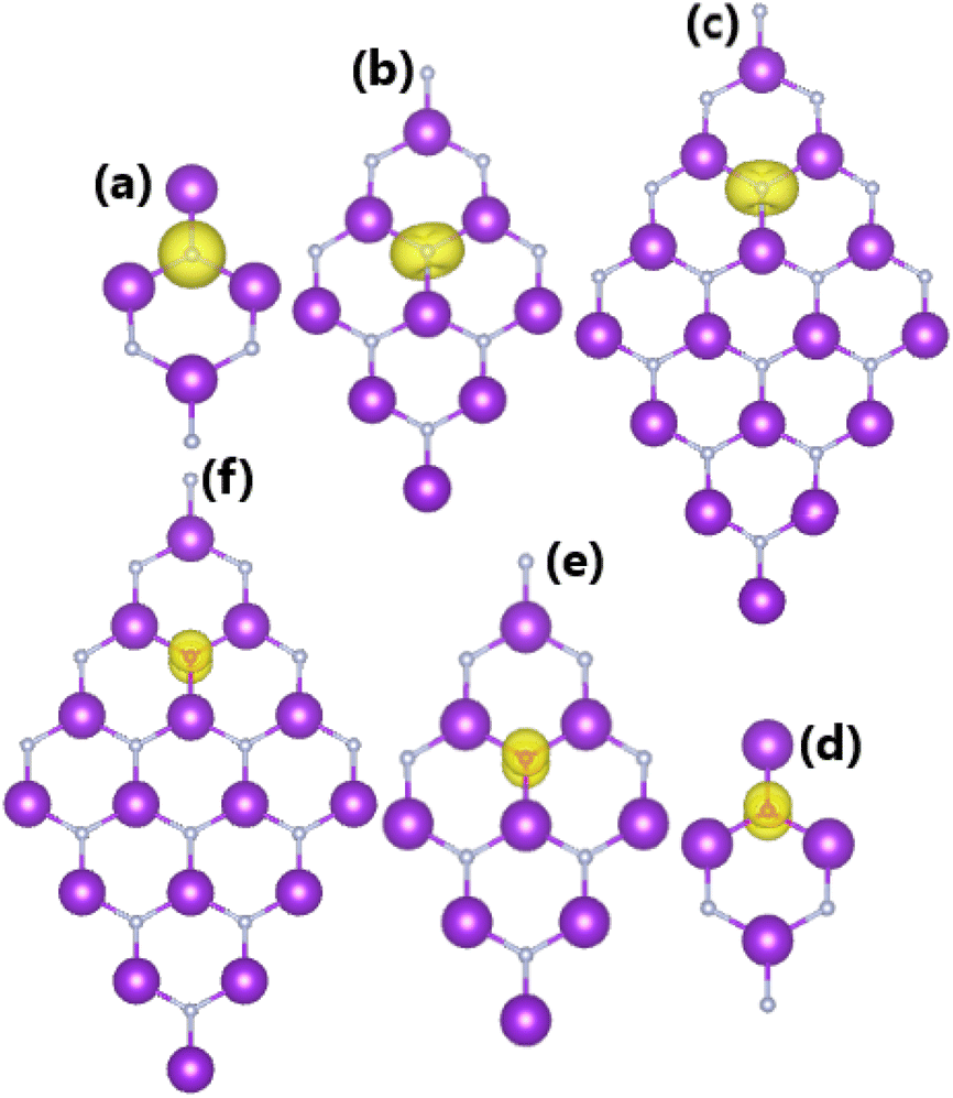
Using the graphene structure as a prototype, a KF monolayer in a planar honeycomb arrangement is predicted. Fig. 1a shows a unit cell that contains two (K and F) inequivalent atoms and belongs to the P![[6 with combining macron]](https://www.rsc.org/images/entities/char_0036_0304.gif) m2 space group (no. 187). After full relaxation, the optimized lattice constant and chemical bond length are a = 4.33 Å and dK−F = 2.50 Å, respectively. Further analysis of stability is based on phonon dispersion curves and ab initio molecular dynamics (AIMD). The phonon spectra displayed in Fig. 1b suggest good dynamical stability of the KF monolayer due to the absence of an imaginary phonon frequency. In addition, its thermal stability is confirmed by AIMD simulations, which indicate structural stability at 300 K over a large time range of up to 3000 fs, without any structural destruction (see Fig. 1c).
m2 space group (no. 187). After full relaxation, the optimized lattice constant and chemical bond length are a = 4.33 Å and dK−F = 2.50 Å, respectively. Further analysis of stability is based on phonon dispersion curves and ab initio molecular dynamics (AIMD). The phonon spectra displayed in Fig. 1b suggest good dynamical stability of the KF monolayer due to the absence of an imaginary phonon frequency. In addition, its thermal stability is confirmed by AIMD simulations, which indicate structural stability at 300 K over a large time range of up to 3000 fs, without any structural destruction (see Fig. 1c).
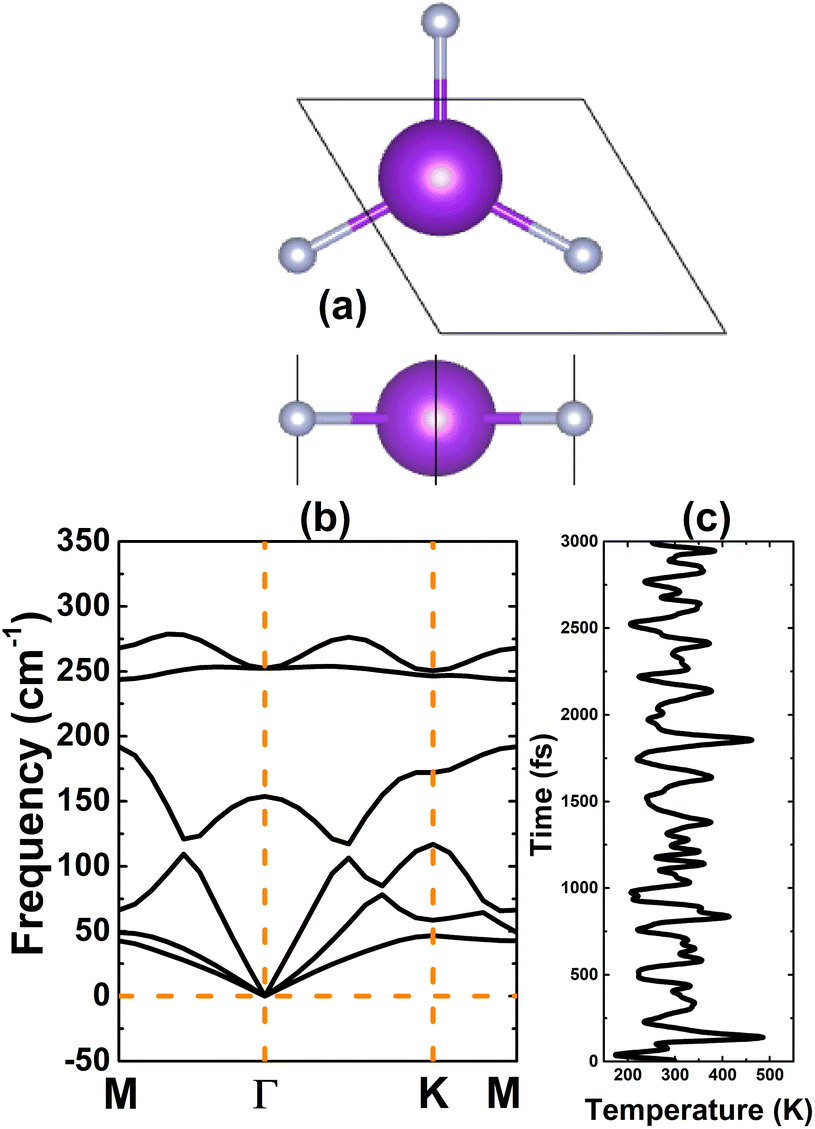 | ||
| Fig. 1 (a) A unit cell (K: violet ball; F: grey ball), (b) phonon dispersion curves, and (c) AIMD simulations of the KF monolayer at 300 K. | ||
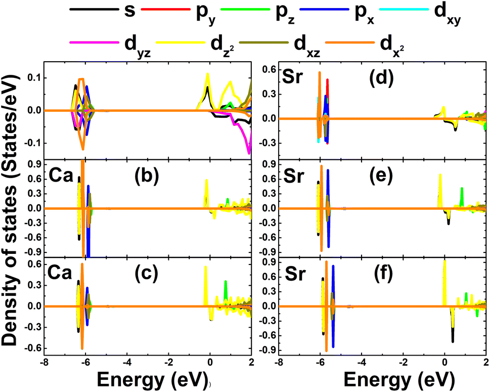
Fig. 2a shows the electronic band structure of the KF monolayer. Having the valence band maximum at the K point and conduction band minimum at the Γ point, the KF monolayer is an indirect-gap insulator with large band gaps of 4.80 and 6.53 eV, as calculated using the PBE and HSE06 functionals, respectively. The contribution of each constituent atom to the band structure formation is analyzed through the projected density of states (PDOS) in Fig. 2b. Note that in the energy range from −2 to 8 eV, the valence band originates mainly from the occupied F-2p orbital with a key role from the pz state, while the unoccupied K-4s orbital dominates the conduction band. These PDOS profiles are characteristic of ionic materials, where the ionic character of the KF monolayer is produced by the charge transfer from the K-4s orbital to the F-2p orbital. This feature is also confirmed by the distribution of valence charge, as illustrated in Fig. 2c, where one can see a large charge accumulation at the F site. From the Bader charge analysis, it is found that a charge amount of 1.12e is involved in the charge-transfer process.
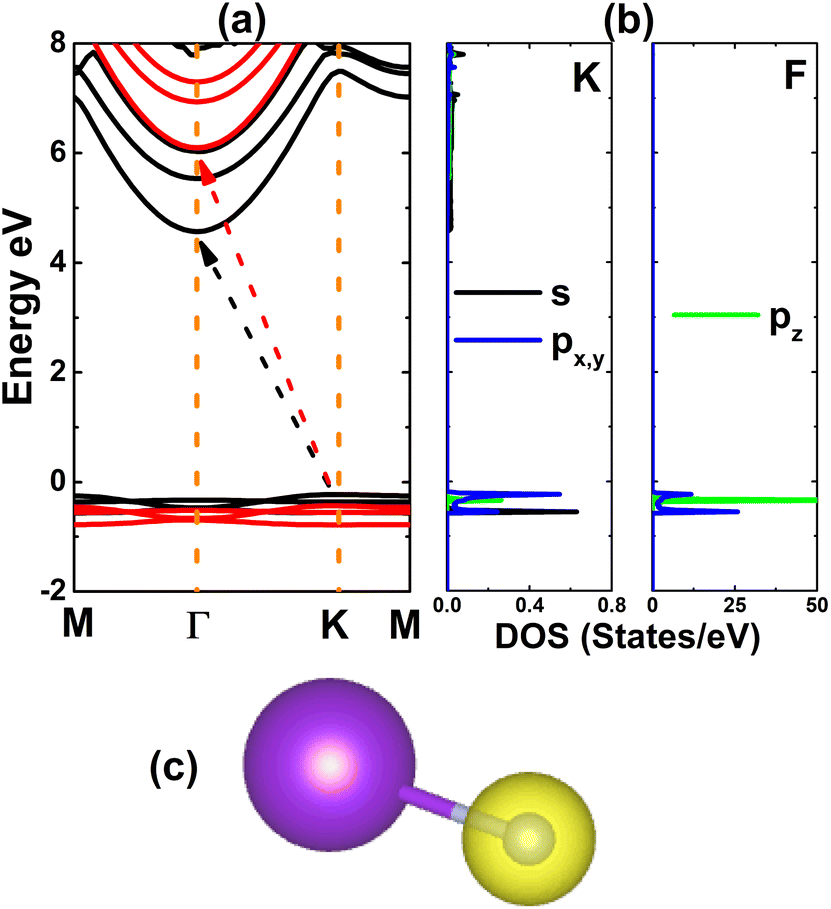 | ||
| Fig. 2 (a) Electronic band structure calculated with the PBE (black curve) and HSE06 (red curve) functionals, (b) projected density of states, and (c) charge distribution (iso-surface value: 0.15 e Å−3) of the KF monolayer. | ||
To investigate the effects of doping, one host atom is replaced with one dopant atom in 2 × 2 × 1, 3 × 3 × 1, and 4 × 4 × 1 supercells to get doping levels of 25%, 11.11%, and 6.25%, respectively. The doping energy, Ed, is calculated as follows:
 | (1) |
| E d | E g | ΔQ | M t | |
|---|---|---|---|---|
| N- | ||||
| 25% | 8.49 | 3.50/M | −0.78 | 2.00 |
| 11.11% | 8.28 | 2.70/0.86 | −0.80 | 2.00 |
| 6.25% | 8.26 | 2.70/0.86 | −0.80 | 2.00 |
![[thin space (1/6-em)]](https://www.rsc.org/images/entities/char_2009.gif) |
||||
| O- | ||||
| 25% | 3.65 | 3.87/0.79 | −0.84 | 1.00 |
| 11.11% | 3.64 | 3.89/0.81 | −0.83 | 1.00 |
| 6.25% | 3.61 | 3.89/0.81 | −0.83 | 1.00 |
|
||||
| Ca- | ||||
| 25% | −0.26 | 0.44/5.16 | +1.22 | 1.06 |
| 11.11% | −0.42 | 0.55/4.70 | +1.17 | 1.00 |
| 6.25% | −0.45 | 0.55/4.64 | +1.16 | 1.00 |
|
||||
| Sr- | ||||
| 25% | 0.04 | 0.08/5.05 | +1.14 | 1.05 |
| 11.11% | −0.35 | 0.65/4.69 | +1.15 | 1.00 |
| 6.25% | −0.36 | 0.63/4.64 | +1.14 | 1.00 |
| E d | E g | ΔQ | M t | |
|---|---|---|---|---|
| N/O- | 12.02 | 3.22/0.56 | −0.66/−0.98 | 3.00 |
| Ca/N- | 7.74 | 0.80/0.33 | +1.31/−1.05 | 2.19 |
| Ca/O- | 2.51 | 0.30/0.23 | +1.46/−1.32 | 0.61 |
| Sr/N- | 7.93 | 0.90/0.31 | +1.32/−1.05 | 2.18 |
| Sr/O- | 2.68 | 0.32/0.27 | +1.47/−1.30 | 0.70 |
| Ca/Sr- | 0.66 | 0.41/4.67 | +1.18/+1.15 | 2.00 |
B. Effects of doping with N and O at anion sites
Table 1 gives the calculated doping energy of N and O in the KF monolayer. It can be noted that this parameter decreases slightly with a reduction in the doping level. Despite their similar atomic size, doping with O is energetically more favorable than doping with N, which may be a result of the electronegativity difference in the O–F pair being smaller than that of the N–F pair.58 However, all the doped systems are thermally stable, without any temperature-induced chemical bond breaking, as confirmed by the AIMD results displayed in Fig. 3. It appears that the thermal stability may be higher at low doping levels, which is reflected in the smaller temperature fluctuations.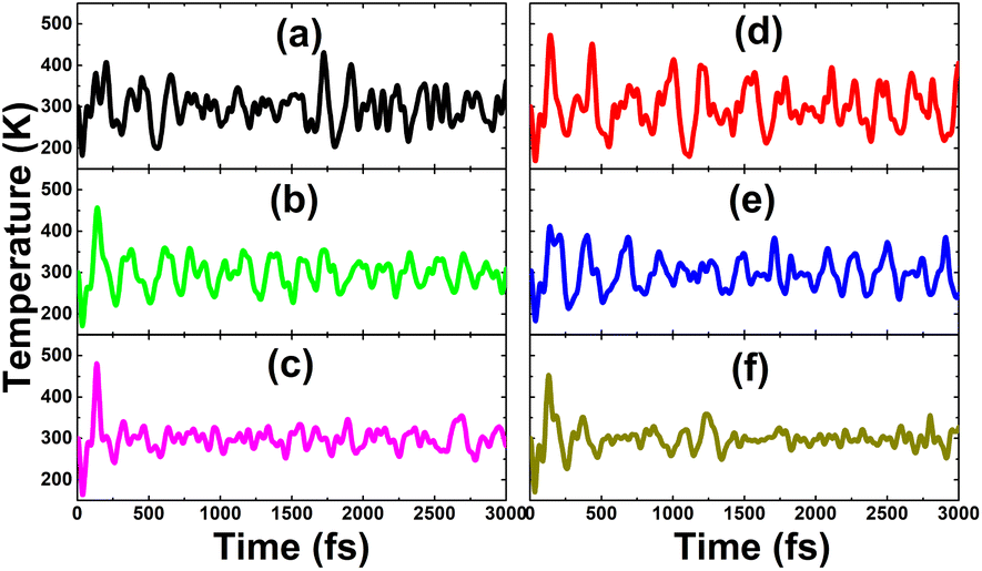 | ||
| Fig. 3 AIMD simulations (at 300 K) of KF monolayers doped with (a) 25%, (b) 11.11%, and (c) 6.25% N; and (d) 25%, (e) 11.11%, and (f) 6.25% O. | ||
The spin-polarized band structures of the N- and O-doped KF monolayers are displayed in Fig. 4. An effective doping-induced modification of the KF monolayer can be noted, with the generation of new middle-gap energy states in both the valence band and conduction band. Half-metallicity is obtained by doping with 25% N, formed by the semiconductor spin-up state and metallic spin-down state (due to the overlap of the new energy branches and the Fermi level). Meanwhile, a magnetic-semiconductor nature emerges in the remaining cases. The spin-dependent energy gaps are listed in Table 1. New energy states in the lower part of the conduction band and upper part of the valence band give rise to smaller band gaps of the spin-down configuration than those of the spin-up counterpart. These doping-induced feature-rich electronic properties suggest the doped systems to be prospective 2D spintronic materials, which can be used to generate spin current.59 Due to their considerably large electronegativity (as compared to K atoms), N and O dopants may receive the charge transferred from the host K-neighbor atoms. This process is quantified through Bader charge analysis. The results (given in Table 1) indicate that the N dopant gains between 0.78 and 0.80e, while a charge quantity of between 0.83 and 0.84e is transferred to the O dopant.
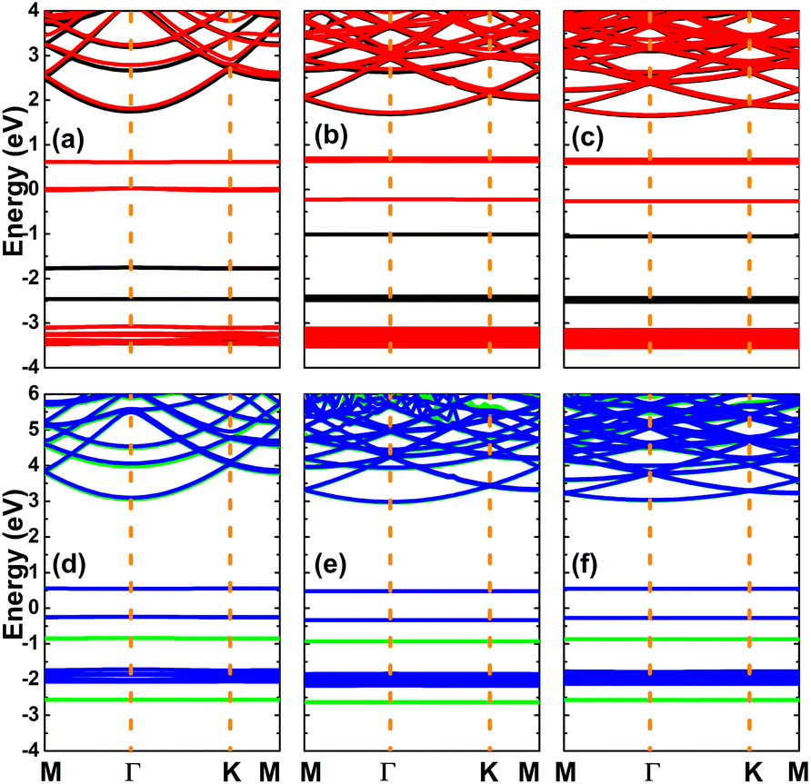 | ||
| Fig. 4 Spin-polarized band structure (spin-up: black and green curves; spin-down: red and blue curves) of KF monolayers doped with (a) 25%, (b) 11.11%, and (c) 6.25% N; and (d) 25%, (e) 11.11%, and (f) 6.25% O. | ||
The analyzed spin-asymmetry of the band structures gives evidence of doping-induced magnetization. The emergence of magnetism is confirmed by total magnetic moments of 2.00 and 1.00 μB in the N- and O-doped KF monolayers, respectively. To get insights into the origin of the magnetism in these systems, the spin density and PDOS spectra of the magnetizing atoms are calculated. Specifically:
• The spin density diagram in Fig. 5 indicates the key role of the dopants in producing magnetic properties, considering a large spin accumulation generated by the difference in charge distribution between the spin channels at their sites.
 | ||
| Fig. 5 Spin density (iso-surface value: 0.004 e Å−3) in (a–c) N- and (d–f) O-doped KF monolayer with doping level of 25%, 11.11%, and 6.25%. | ||
• The PDOS spectra of N and O atoms given in Fig. 6 confirm that the magnetism originates mainly from their 2p orbitals. Remember that N and O atoms have 2s22p3 and 2p22p4 valence electron configurations, respectively. Therefore, after receiving about 1e from the host monolayer, the N atom has 2 unoccupied states, leading to a total magnetic moment of 2 μB. Meanwhile, this number is 1 μB in the case of O doping.
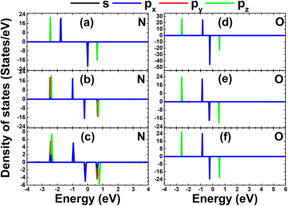 | ||
| Fig. 6 Projected density of states of dopants in KF monolayers doped with (a) 25%, (b) 11.11%, and (c) 6.25% N; and (d) 25%, (e) 11.11%, and (f) 6.25% O. | ||
C. Effects of doping with Ca and Sr at cation sites
Herein, doping at the cation sites of the KF monolayer is considered. The doping energies of Ca and Sr atoms are listed in Table 1. Except for 25% N, the doping processes are exothermic as suggested by the negative doping energies. Ca doping may be easier to realize than Sr doping due to its more negative doping energy. For both cases, a high doping level requires more energy, since the doping energy becomes more positive with the increase in the dopant concentration. Further AIMD simulations indicate good thermal stability of the Ca- and Sr-doped KF monolayers, exhibiting no temperature-induced structural destruction up to 3000 fs (see Fig. 7). Similar to previous cases, low-doping systems may be thermally more stable than highly doped ones, considering the smaller temperature fluctuations shown by AIMD simulations. The calculated spin-polarized band structures of the Ca- and Sr-doped KF monolayers are displayed in Fig. 8. Both spin states exhibit semiconductor character; however, the spin asymmetry induced by new middle-gap flat energy branches gives rise to the development of a magnetic-semiconductor nature. The spin-dependent band gaps are listed in Table 1. In contrast to the previous cases of doping with N and O, the spin-up energy gaps are smaller than the spin-down energy gaps due to the appearance of energy states around the Fermi level (below the Fermi level for the spin-up channel and above the Fermi level for the spin-down channel). In addition, acting as cations in the doped systems, Ca and Sr dopants may transfer a certain amount of charge to their nearest host F atoms due to their considerably lower electronegativity. A study based on Bader charge analysis indicates the transfer of 0.16–0.22e and 0.14–0.15e from the Ca and Sr atoms to the host monolayer once they are substitutionally incorporated (see Table 1).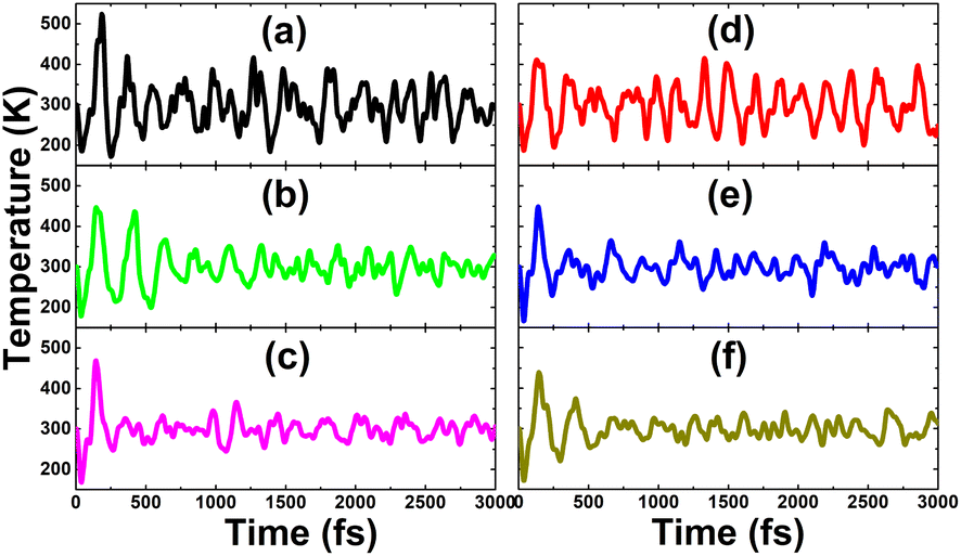 | ||
| Fig. 7 AIMD simulations (at 300 K) of KF monolayers doped with (a) 25%, (b) 11.11%, and (c) 6.25% Ca; and (d) 25%, (e) 11.11%, and (f) 6.25% Sr. | ||
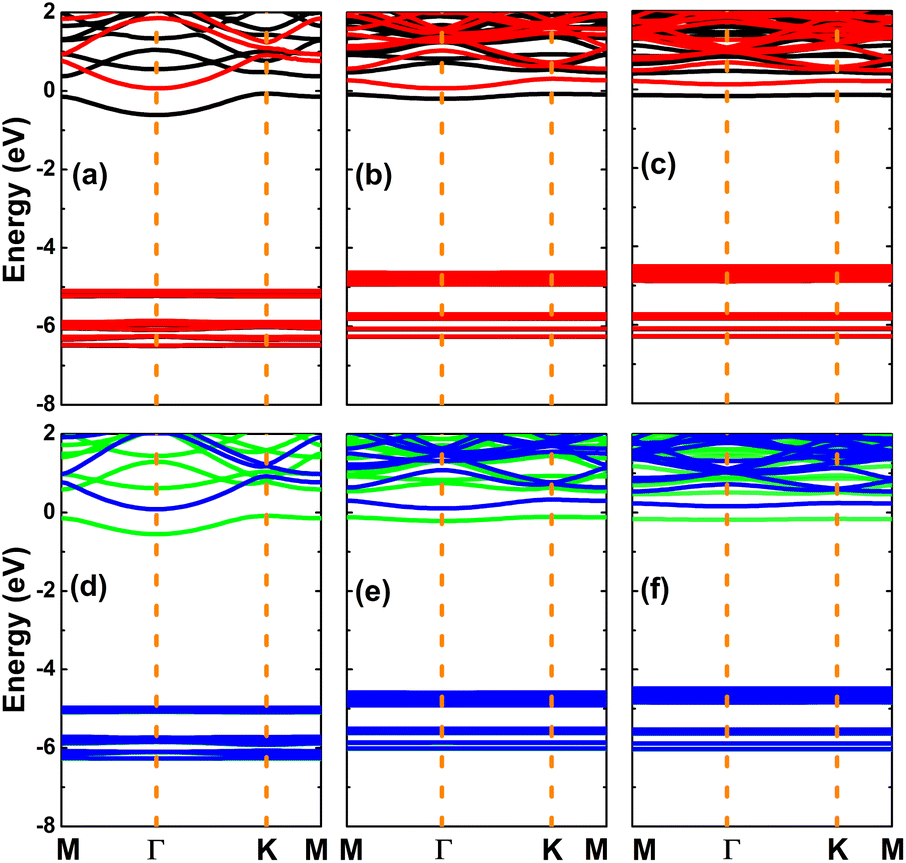 | ||
| Fig. 8 Spin-polarized band structure (spin-up: black and green curves; spin-down: red and blue curves) of KF monolayers doped with (a) 25%, (b) 11.11%, and (c) 6.25% Ca; and (d) 25%, (e) 11.11%, and (f) 6.25% Sr. | ||
Despite their similar quantities of transferred charge, Ca/Sr and K atoms have different valence electron configurations (3d04s2/4d05s2 and 3d04s1, respectively). Therefore, the replacement of K atoms by Ca and Sr atoms may significantly magnetize the KF monolayer, which has been evidenced by the spin-asymmetric band structures. Moreover, our calculations yield total magnetic moments of 1 μB, and this parameter increases slightly at a high doping level of 25% for Ca and Sr, to 1.06 and 1.05 μB, respectively. The results for the spin density in Fig. 9 and PDOS in Fig. 10 provide a deeper understanding of the origin of the magnetism. Precisely:
• The spin density has been calculated as the difference between the spin-up and spin-down charge distributions. The illustration of the spin density in Fig. 9 indicates that the difference occurs mainly at the Ca and Sr sites, confirming their role as magnetizing agents.
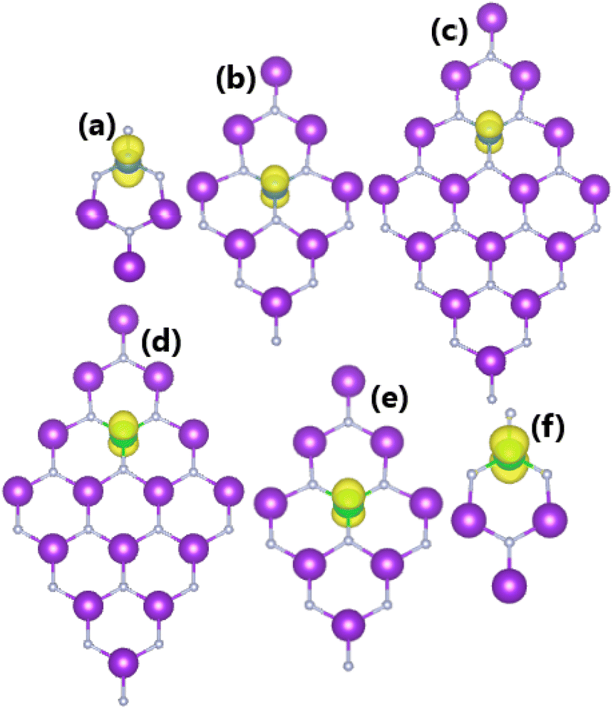 | ||
| Fig. 9 Spin density (iso-surface value: 0.002 e Å−3) in (a–c) Ca- and (d–f) Sr-doped KF monolayers with doping level of 25%, 11.11%, and 6.25%. | ||
• The PDOS spectra of the Ca and Sr dopants in Fig. 10 indicate that, in the considered energy range, they contribute to both the valence band and conduction band. Most importantly, the energy states around the Fermi level are formed mainly from Ca-3dz2, Ca-4s, Sr-4dz2, and Sr-5s states with a clear spin asymmetry. Therefore, one can conclude that these mentioned electronic states are the main origin of the magnetism in the Ca- and Sr-doped KF monolayers.
 | ||
| Fig. 10 Projected density of states of dopants in KF monolayers doped with (a) 25%, (b) 11.11%, and (c) 6.25% Ca; and (d) 25%, (e) 11.11%, and (f) 6.25% Sr. | ||
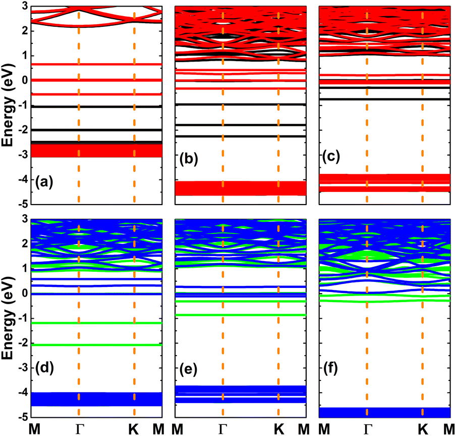
D. Effects of codoping
In this part, the effects of codoping with N/O, Ca/N, Ca/O, Sr/N, Sr/O, and Sr/Ca on the electronic and magnetic properties of the KF monolayer are investigated. Firstly, the doping energies are calculated, and these results are given in Table 2. As expected, charge donors Ca and Sr will significantly decrease this parameter, such that the smallest value of 0.66 eV is obtained for Ca/Sr codoping. Meanwhile, simultaneous substitution of two F atoms by N and O charge acceptors requires the largest doping energy of 12.02 eV.Fig. 11 shows the spin-polarized band structures of the codoped systems. It can be clearly noted that there is spin asymmetry as a consequence of new energy states, which are developed in the forbidden energy range of the host KF monolayer. As such, a magnetic-semiconductor nature is obtained in all six cases, and is generated by semiconductor character in both spin states. Table 2 gives the spin-dependent band gaps. Note that the N/O-codoped monolayer has a large spin-up energy gap and small spin-down energy gap, and the opposite feature is obtained via Ca/Sr codoping (similar to the previous cases of single-atom doping). However, the synergistic effects of codoping at both cation and anion sites leads to small (less than 1 eV) band gaps in both spin configurations. With the exception of the N dopant in the case of the N/O-codoped KF monolayer, the involvement of two dopants induces an increase in the transferred charge, as shown by the Bader charge analysis, whose numerical results are given in Table 2.
 | ||
| Fig. 11 Spin-polarized band structure (spin-up: black and green curves; spin-down: red and blue curves) of KF monolayers codoped with (a) N/O, (b) Ca/N, (c) Ca/O, (d) Sr/N, (e) Sr/O, and (f) Ca/Sr. | ||
Codoping with N/O and Ca/Sr magnetizes the KF monolayer, with total magnetic moments of 3.00 and 2.00 μB, respectively. Herein, all dopant atoms play a key role in producing magnetic properties, as confirmed by the spin density illustrated in Fig. 12a and f. Furthermore, magnetism also emerges in Ca/N-, Ca/O-, Sr/N-, and Sr/O-codoped systems, with total magnetic moments of 2.19, 0.61, 2.18, and 0.70 μB, respectively. Fig. 12b–e show that in these cases, magnetism originates mainly from N and O atoms, while Ca and Sr atoms exhibit weaker influences on the magnetic properties. Undoubtedly, the electronic and magnetic properties of the codoped systems are regulated mainly by the N-2p, O-2p, Ca-3d, Ca-4s, Sr-4d, and Sr-5s orbitals, similar to the previous cases of separate dopings.
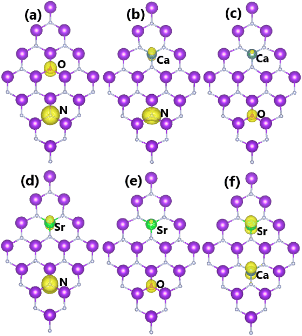 | ||
| Fig. 12 Spin density (iso-surface value: 0.002 e Å−3) in KF monolayers codoped with (a) N/O, (b) Ca/N, (c) Ca/O, (d) Sr/N, (e) Sr/O, and (f) Ca/Sr. | ||
IV. Conclusions
In summary, first-principles calculations have been performed to predict the KF monolayer as well as investigate the effects of doping on its electronic and magnetic properties. The KF monolayer is predicted to have good stability, adopting a planar graphene-like honeycomb structure. Electronic calculations indicate insulating and ionic characters without intrinsic magnetism, where the valence band and conduction band are formed mainly by F-2p and K-4s orbitals, respectively. Doping with N/O at anion sites and Ca/Sr at cation sites is considered in order to induce magnetic properties. The calculations of doping energy indicate that replacing a K atom is energetically more favorable than replacing an F atom. Bader charge analysis indicates a charge gain of N and O dopants from the host monolayer, while Ca and Sr dopants act as charge donors, transferring significant amounts of charge to the host monolayer. The modified electronic interactions lead to the appearance of new middle-gap energy states, which originate from the N-2p, O-2p, Ca-3d, Ca-4s, Sr-4d and Sr-5s orbitals due to their partial occupancy. Consequently, they produce mainly magnetic properties in the doped systems. The codoped KF monolayers have also been investigated, and exhibit magnetic semiconductor behavior, similar to the cases of single-atom doping. In the cases of the N/O- and Ca/Sr-codoped systems, all dopants act as magnetizing agents. Meanwhile, only N and O atoms play a dominant role in the origin of the magnetism in the Ca/N-, Ca/O-, Sr/N-, and Sr/O-codoped systems, where Ca and Sr exhibit weak influences. In addition, AIMD simulations confirm good thermal stability of the doped and codoped systems at room temperature. The results presented herein pave a solid path, based on doping, to functionalize new ionic KF monolayers for spintronic applications; this is not accounted for by the pristine monolayer, which has no intrinsic magnetism or suitable electronic structures.Conflicts of interest
The authors declare that they have no known competing financial interests or personal relationships that could have appeared to influence the work reported in this paper.Acknowledgements
Calculations were performed at the DGCTIC-UNAM Supercomputing Center (project LANCAD-UNAM-DGTIC-368).References
- K. S. Novoselov, Z. Jiang, Y. Zhang, S. Morozov, H. L. Stormer, U. Zeitler, J. Maan, G. Boebinger, P. Kim and A. K. Geim, Room-temperature quantum hall effect in graphene, Science, 2007, 315(5817), 1379 CrossRef CAS PubMed.
- A. A. Balandin, S. Ghosh, W. Bao, I. Calizo, D. Teweldebrhan, F. Miao and C. N. Lau, Superior thermal conductivity of single-layer graphene, Nano Lett., 2008, 8(3), 902–907 CrossRef CAS PubMed.
- M. A. Brown, M. S. Crosser, M. R. Leyden, Y. Qi and E. D. Minot, Measurement of high carrier mobility in graphene in an aqueous electrolyte environment, Appl. Phys. Lett., 2016, 109(9), 093104 CrossRef.
- K. S. Novoselov, A. K. Geim, S. V. Morozov, D.-e. Jiang, Y. Zhang, S. V. Dubonos, I. V. Grigorieva and A. A. Firsov, Electric field effect in atomically thin carbon films, Science, 2004, 306(5696), 666–669 CrossRef CAS PubMed.
- L. Kong, A. Enders, T. S. Rahman and P. A. Dowben, Molecular adsorption on graphene, J. Phys.: Condens. Matter, 2014, 26(44), 443001 CrossRef PubMed.
- J. Yang, P. Hu and G. Yu, Perspective of graphene-based electronic devices: Graphene synthesis and diverse applications, APL Mater., 2019, 7(2), 020901 CrossRef.
- J. M. Tour, Top-down versus bottom-up fabrication of graphene-based electronics, Chem. Mater., 2014, 26(1), 163–171 CrossRef CAS.
- F. Bonaccorso, Z. Sun, T. Hasan and A. Ferrari, Graphene photonics and optoelectronics, Nat. Photonics, 2010, 4(9), 611–622 CrossRef CAS.
- P. Avouris and M. Freitag, Graphene photonics, plasmonics, and optoelectronics, IEEE J. Sel. Top. Quantum Electron., 2014, 20(1), 72–83 Search PubMed.
- S. S. Varghese, S. Lonkar, K. Singh, S. Swaminathan and A. Abdala, Recent advances in graphene based gas sensors, Sens. Actuators, B, 2015, 218, 160–183 CrossRef CAS.
- W. Yuan and G. Shi, Graphene-based gas sensors, J. Mater. Chem. A, 2013, 1(35), 10078–10091 RSC.
- W. Han, R. K. Kawakami, M. Gmitra and J. Fabian, Graphene spintronics, Nat. Nanotechnol., 2014, 9(10), 794–807 CrossRef CAS PubMed.
- P. Seneor, B. Dlubak, M.-B. Martin, A. Anane, H. Jaffres and A. Fert, Spintronics with graphene, MRS Bull., 2012, 37(12), 1245–1254 CrossRef CAS.
- M. F. El-Kady, Y. Shao and R. B. Kaner, Graphene for batteries, supercapacitors and beyond, Nat. Rev. Mater., 2016, 1(7), 16033 CrossRef CAS.
- M. Yu, R. Li, M. Wu and G. Shi, Graphene materials for lithium–sulfur batteries, Energy Storage Mater., 2015, 1, 51–73 CrossRef.
- C. Huang, C. Li and G. Shi, Graphene based catalysts, Energy Environ. Sci., 2012, 5(10), 8848–8868 RSC.
- B. F. Machado and P. Serp, Graphene-based materials for catalysis, Catal. Sci. Technol., 2012, 2(1), 54–75 RSC.
- A. Gupta, T. Sakthivel and S. Seal, Recent development in 2D materials beyond graphene, Prog. Mater. Sci., 2015, 73, 44–126 CrossRef CAS.
- R. Mas-Balleste, C. Gomez-Navarro, J. Gomez-Herrero and F. Zamora, 2D materials: to graphene and beyond, Nanoscale, 2011, 3(1), 20–30 RSC.
- H. Li, J. Wu, Z. Yin and H. Zhang, Preparation and applications of mechanically exfoliated single-layer and multilayer MoS2 and WSe2 nanosheets, Acc. Chem. Res., 2014, 47(4), 1067–1075 CrossRef CAS PubMed.
- W. Zhu, X. Gao, Q. Li, H. Li, Y. Chao, M. Li, S. M. Mahurin, H. Li, H. Zhu and S. Dai, Controlled gas exfoliation of boron nitride into few-layered nanosheets, Angew. Chem., 2016, 128(36), 10924–10928 CrossRef.
- S. Wild, V. Lloret, V. Vega-Mayoral, D. Vella, E. Nuin, M. Siebert, M. Koleśnik-Gray, M. Löffler, K. J. Mayrhofer and C. Gadermaier, et al., Monolayer black phosphorus by sequential wet-chemical surface oxidation, RSC Adv., 2019, 9(7), 3570–3576 RSC.
- J. M. Garcia, U. Wurstbauer, A. Levy, L. N. Pfeiffer, A. Pinczuk, A. S. Plaut, L. Wang, C. R. Dean, R. Buizza and A. M. Van Der Zande, et al., Graphene growth on h-BN by molecular beam epitaxy, Solid State Commun., 2012, 152(12), 975–978 CrossRef CAS.
- X. Chen, L. Zhang and S. Chen, Large area CVD growth of graphene, Synth. Met., 2015, 210, 95–108 CrossRef CAS.
- W. Zhang, J.-K. Huang, C.-H. Chen, Y.-H. Chang, Y.-J. Cheng and L.-J. Li, High-gain phototransistors based on a CVD MoS2 monolayer, Adv. Mater., 2013, 25(25), 3456–3461 CrossRef CAS PubMed.
- B. Liu, M. Fathi, L. Chen, A. Abbas, Y. Ma and C. Zhou, Chemical vapor deposition growth of monolayer WSe2 with tunable device characteristics and growth mechanism study, ACS Nano, 2015, 9(6), 6119–6127 CrossRef CAS PubMed.
- L. Jiao, H. J. Liu, J. Chen, Y. Yi, W. Chen, Y. Cai, J. Wang, X. Dai, N. Wang and W. K. Ho, et al., Molecular-beam epitaxy of monolayer MoSe2: growth characteristics and domain boundary formation, New J. Phys., 2015, 17(5), 053023 CrossRef.
- F. Ullah, T. K. Nguyen, C. T. Le and Y. S. Kim, Pulsed laser deposition assisted grown continuous monolayer MoSe2, CrystEngComm, 2016, 18(37), 6992–6996 RSC.
- K. K. Kim, A. Hsu, X. Jia, S. M. Kim, Y. Shi, M. Hofmann, D. Nezich, J. F. Rodriguez-Nieva, M. Dresselhaus and T. Palacios, et al., Synthesis of monolayer hexagonal boron nitride on Cu foil using chemical vapor deposition, Nano Lett., 2012, 12(1), 161–166 CrossRef PubMed.
- D. Velázquez, R. Seibert, H. Man, L. Spentzouris and J. Terry, Pulsed laser deposition of single layer, hexagonal boron nitride (white graphene, h-BN) on fiber-oriented Ag (111)/SrTiO3(001), J. Appl. Phys., 2016, 119(9), 095306 CrossRef.
- W. Zhang, H. Enriquez, Y. Tong, A. Bendounan, A. Kara, A. P. Seitsonen, A. J. Mayne, G. Dujardin and H. Oughaddou, Epitaxial synthesis of blue phosphorene, Small, 2018, 14(51), 1804066 CrossRef PubMed.
- J. B. Smith, D. Hagaman and H.-F. Ji, Growth of 2D black phosphorus film from chemical vapor deposition, Nanotechnology, 2016, 27(21), 215602 CrossRef PubMed.
- C. M. Polley, H. Fedderwitz, T. Balasubramanian, A. A. Zakharov, R. Yakimova, O. Bäcke, J. Ekman, S. P. Dash, S. Kubatkin and S. Lara-Avila, Bottom-upgrowth of monolayer honeycomb SiC, Phys. Rev. Lett., 2023, 130, 076203 CrossRef CAS PubMed.
- H. Zhang, M. Holbrook, F. Cheng, H. Nam, M. Liu, C.-R. Pan, D. West, S. Zhang, M.-Y. Chou and C.-K. Shih, Epitaxial growth of two-dimensional insulator monolayer honeycomb BeO, ACS Nano, 2021, 15(2), 2497–2505 CrossRef CAS PubMed.
- H. Şahin, S. Cahangirov, M. Topsakal, E. Bekaroglu, E. Akturk, R. T. Senger and S. Ciraci, Monolayer honeycomb structures of group-IV elements and III–V binary compounds: First-principles calculations, Phys. Rev. B: Condens. Matter Mater. Phys., 2009, 80(15), 155453 CrossRef.
- H. Zheng, X.-B. Li, N.-K. Chen, S.-Y. Xie, W. Q. Tian, Y. Chen, H. Xia, S. Zhang and H.-B. Sun, Monolayer II–VI semiconductors: A first-principles prediction, Phys. Rev. B: Condens. Matter Mater. Phys., 2015, 92(11), 115307 CrossRef.
- B. Luo, Y. Yao, E. Tian, H. Song, X. Wang, G. Li, K. Xi, B. Li, H. Song and L. Li, Graphene-like monolayer monoxides and monochlorides, Proc. Natl. Acad. Sci., 2019, 116(35), 17213–17218 CrossRef CAS PubMed.
- D. Hoat, M. Naseri, N. T. Binh, J. Rivas-Silva, T. V. Vu and G. H. Cocoletzi, LiCl monolayer for UV detection: first principles prediction, Phys. E, 2020, 123, 114168 CrossRef CAS.
- M. Flórez, J. Recio, E. Francisco, M. Blanco and A. M. Pendás, First-principles study of the rocksalt–cesium chloride relative phase stability in alkali halides, Phys. Rev. B: Condens. Matter Mater. Phys., 2002, 66(14), 144112 CrossRef.
- A. M. Pendás, V. Luana, J. Recio, M. Flórez, E. Francisco, M. Blanco and L. Kantorovich, Pressure-induced B1-B2 phase transition in alkali halides: General aspects from first-principles calculations, Phys. Rev. B: Condens. Matter Mater. Phys., 1994, 49(5), 3066 CrossRef PubMed.
- Z. Cui, K. Yang, K. Ren, S. Zhang and L. Wang, Adsorption of metal atoms on MoSi2N4 monolayer: A first principles study, Mater. Sci. Semicond. Process., 2022, 152, 107072 CrossRef CAS.
- K. Yang, Z. Cui, E. Li, Y. Shen, L. Zhang, D. Ma, Z. Yuan, Y. Dong and S. Zhang, Modulation of the magnetic, electronic, and optical behaviors of WS2 after metals adsorption: a first-principles study, Chem. Phys., 2023, 571, 111903 CrossRef CAS.
- Z. Cui and H. Wu, Metal atoms adsorbed Ga2O3 monolayer: as a potential application in optoelectronic devices, Micro Nanostruct., 2023, 180, 207613 CrossRef CAS.
- R. Caglayan, Y. Mogulkoc, A. Mogulkoc, M. Modarresi and A. Rudenko, Easy-axis rotation in ferromagnetic monolayer CrN induced by fluorine and chlorine functionalization, Phys. Chem. Chem. Phys., 2022, 24(41), 25426–25433 RSC.
- A. Mogulkoc, Y. Mogulkoc, D. Keçik and E. Durgun, The effect of strain and functionalization on the optical properties of borophene, Phys. Chem. Chem. Phys., 2018, 20(32), 21043–21050 RSC.
- Z. Cui, K. Yang, Y. Shen, Z. Yuan, Y. Dong, P. Yuan and E. Li, Toxic gas molecules adsorbed on intrinsic and defective WS2: gas sensing and detection, Appl. Surf. Sci., 2023, 613, 155978 CrossRef CAS.
- Y. Zengin, R. Caglayan and Y. Mogulkoc, Adsorption of Small Gas Molecules onto the Two-Dimensional Janus SnSSe Monolayer, Computational Condensed Matter ( 2023) e00815 Search PubMed.
- M. Pizzochero and O. V. Yazyev, Point defectsin the 1T′ and 2H phases of single-layer MoS2: a comparative first-principles study, Phys. Rev. B, 2017, 96(24), 245402 CrossRef.
- V. Van On, J. Guerrero-Sanchez, R. Ponce-Pérez, T. V. Vu, J. Rivas-Silva, G. H. Cocoletzi and D. Hoat, Defective and doped MgO monolayer as promising 2D materials for optoelectronic and spintronic applications, Mater. Sci. Semicond. Process., 2022, 149, 106876 CrossRef CAS.
- D. Ma, H. Wei, Y. Shen, Z. Cui, E. Li and L. Zhang, Effect of alkaline earth metals doping on the electronic structure, magnetic and optical properties of g-SiC monolayer system by first principles calculation, in Journal of Physics: Conference Series, IOP Publishing, 2022, vol. 2329, p. 012046 Search PubMed.
- D. Hoat, D. K. Nguyen, J. Guerrero-Sanchez, R. Ponce-Pérez, V. Van On, J. Rivas-Silva and G. H. Cocoletzi, Engineering the electronic and magnetic properties of nitrogen monolayer and bilayer by doping: a first-principles study, Appl. Surf. Sci., 2021, 566, 150711 CrossRef CAS.
- W. Kohn and L. J. Sham, Self-consistent equations including exchange and correlation effects, Phys. Rev., 1965, 140(4A), A1133 CrossRef.
- G. Kresse and J. Furthmüller, Efficiency of ab-initio total energy calculations for metals and semiconductors using a plane-wave basis set, Comput. Mater. Sci., 1996, 6(1), 15–50 CrossRef CAS.
- G. Kresse and J. Furthmüller, Efficient iterative schemes for ab initio total-energy calculations using a plane-wave basis set, Phys. Rev. B: Condens. Matter Mater. Phys., 1996, 54(16), 11169 CrossRef CAS PubMed.
- J. P. Perdew, K. Burke and M. Ernzerhof, Generalized gradient approximation made simple, Phys. Rev. Lett., 1996, 77(18), 3865 CrossRef CAS PubMed.
- A. V. Krukau, O. A. Vydrov, A. F. Izmaylov and G. E. Scuseria, Influence of the exchange screening parameter on the performance of screened hybrid functionals, J. Chem. Phys., 2006, 125(22), 224106 CrossRef PubMed.
- H. J. Monkhorst and J. D. Pack, Special points for Brillouin-zone integrations, Phys. Rev. B: Solid State, 1976, 13(12), 5188 CrossRef.
- R. T. Sanderson, Electronegativity and bond energy, J. Am. Chem. Soc., 1983, 105(8), 2259–2261 CrossRef CAS.
- X. Li and J. Yang, First-principles design of spintronics materials, Natl. Sci. Rev., 2016, 3(3), 365–381 CrossRef CAS.
| This journal is © The Royal Society of Chemistry 2023 |