
 Open Access Article
 This Open Access Article is licensed under a Creative Commons Attribution-Non Commercial 3.0 Unported Licence
A comprehensive review of the current progresses and material advances in perovskite solar cells
Rabia
Sharif
 a,
Arshi
Khalid
b,
Syed Waqas
Ahmad
a,
Abdul
Rehman
a,
Haji Ghulam
Qutab
a,
Hafiz Husnain
Akhtar
a,
Khalid
Mahmood
*a,
Shabana
Afzal
c and
Faisal
Saleem
a
a,
Arshi
Khalid
b,
Syed Waqas
Ahmad
a,
Abdul
Rehman
a,
Haji Ghulam
Qutab
a,
Hafiz Husnain
Akhtar
a,
Khalid
Mahmood
*a,
Shabana
Afzal
c and
Faisal
Saleem
a
aDepartment of Chemical & Polymer Engineering, University of Engineering & Technology Lahore, Faisalabad Campus, 3½ Km. Khurrianwala – Makkuana By-Pass, Faisalabad, Pakistan. E-mail: khalid@uet.edu.pk
bDepartment of Humanities & Basic Sciences, University of Engineering & Technology Lahore, Faisalabad Campus, 3½ Km. Khurrianwala – Makkuana By-Pass, Faisalabad, Pakistan
cDepartment of Basic Sciences, Humanities Muhammad Nawaz Shareef University of Engineering and Technology Multan, Pakistan
First published on 23rd June 2023
Abstract
Recently, perovskite solar cells (PSCs) have attracted ample consideration from the photovoltaic community owing to their continually-increasing power conversion efficiency (PCE), viable solution-processed methods, and inexpensive materials ingredients. Over the past few years, the performance of perovskite-based devices has exceeded 25% due to superior perovskite films achieved using low-temperature synthesis procedures along with evolving appropriate interface and electrode-materials. The current review provides comprehensive knowledge to enhance the performance and materials advances for perovskite solar cells. The latest progress in terms of perovskite crystal structure, device construction, fabrication procedures, and challenges are thoroughly discussed. Also discussed are the different layers such as ETLs and buffer-layers employed in perovskite solar-cells, seeing their transmittance, carrier mobility, and band gap potentials in commercialization. Generally, this review delivers a critical assessment of the improvements, prospects, and trials of PSCs.
1. Introduction
Energy deficiencies have caused a worldwide issue in the 21st century. At present, most of the biosphere's energy is produced from petroleum derivatives such as coal, oil, and natural gas; as per the US Energy Information Organization (EIA), in 2016, ∼65% of power was produced from petroleum derivatives and ∼20% was using thermal power, while just ∼15% was from environmentally-friendly power pathways. The inclination to foster sustainable power innovations (such as wind, sun, hydroelectric and geothermal) to supplant the fossil fuel-based energy age has inspired significant logical studies. Among the diverse sustainable sources, sun-powered energy is one of the greatest encouraging advancements to fulfill the developing worldwide energy demands and to determine or moderate the ever-rising energy emergency because of the consumption of petroleum derivatives.1Just 1% of energy creation was accounted for by the sun-based source as determined in 2013; sun-oriented power is probable to turn into the most critical wellspring of energy by 2050.2 Sunlight-based energy enjoys a few critical upper hands over other sustainable technologies, in particular, the worldwide dispersion of daylight (conversely to wind, hydroelectric and geothermal assets that are contained to specific regions), the absence of unsafe waste generation (rather than thermal power), and the decentralized nature of sun-oriented energy age.3
Tackling renewable energy is obviously the arrangement to the world's taking off energy requests and the current worldwide environment emergency. Sun-oriented energy is the most bountiful renewable asset accessible on the earth.4 Also, it is along these lines broadly contemplated by analysts across the globe. Photovoltaics have radically improved among the first and third ages, diminishing the cost of assembling, while at the same time keeping up with power effectiveness.5
Solar cells are viewed as a significant method for tackling environmental contamination issues and using sustainable power, so different kinds of solar cells have been created. Among them, the slight film solar cells, for example, perovskite solar cells (PSCs) and organic solar cells (OSCs) have drawn extraordinary consideration from analysts because of the benefits of basic assembly, lightweight, and arrangement handling. The certified most noteworthy PCE of single-junction PSCs and OSCs has reached 25.2 and 17.4%, respectively.6
Perovskite, named after the Russian mineralogist L. A. Perovski, has an explicit valuable stone construction with the ABX3 formula (X = oxygen, halogen). The larger A cation occupies a cubo octahedral place common with twelve X anions, though the extra modest B cation is balanced out in an octahedral site imparted to six X anions. The most careful perovskites are oxides owing to their electrical characteristics of superconductivity or ferroelectricity. Halide perovskites attained less attention till coated organometal halide perovskites were testified to display semiconductor-to-metal development with growing dimensionality.7
The critical material for the PSCs as of late generating incredible consideration is the organometal halide CH3NH3MX3 (M = Pb or Sn, X = Cl, Br or I), whose construction and actual characteristics were primarily announced by Weber in 1978.8 For CH3NH3PbX3, there is an increment for the unit cell boundary from 5.68 to 5.92 and to 6.27 Å as the size of the halide goes from X = Cl to Br and to I. Lattice parameters in the cubic stage can be basically tuned by blending halides; for example, CH3NH3PbBr2.3Cl0.7 presented a = 5.98 Å, CH3NH3PbBr2.07I0.93 displayed a = 6.03 Å, and CH3NH3PbBr0.45I2.55 exhibited a = 6.25 Å. CH3NH3SnBrxl3−x (x = 0–3) crystalized to the cubic perovskite assembly with the unit cell parameters a = 5.89 Å (x = 3), a = 6.01 Å (x = 2) and a = 6.24 Å (x = 0). In spite of Pb-based perovskite materials, some Sn-based perovskite materials showed conducting characteristics.9
Organic–inorganic hybrid lead halide perovskites pulled in scientists' considerations during the 1970s and 1990s,8,10 particularly for their remarkable conducting and semiconducting characteristics.11 In 2009, the exploration endeavors to use lead perovskite as a light absorber in solar cells were reported by Miyasaka et al. consolidating CH3NH3PbI3 (MAPbI3) and CH3NH3PbBr3 (MAPbBr3) as sensitizers into color sharpened solar cells (DSSCs), demonstrating 3.8 and 3.1% PCE, respectively.12
Considering the significant source of perfect and feasible energy on the planet, solar flux has for some time been looked to change over into power over the photovoltaic impact of light-retaining semiconductors. Prior age photovoltaics used inorganic translucent semiconductors such as cadmium telluride (CdTe), silicon, and copper indium gallium selenide/sulfide (CIGS) as safeguards; these can be productive and steady, however, generally need high energy-input make, including and high-vacuum high-temperature methods.
The arising natural PSCs address one of the groundbreaking advancements since they are similar to OSCs;13 furthermore, DSSCs, possibly can be fabricated into lightweight, adaptable, and minimal expense power causes through the high-throughput solution construction.14 PSCs have subsequently obtained concentrated exploration endeavors from both the scholarly world and industry. The PCEs of PSCs have quickly improved from 3.8% to 22.1% in only seven years, showing the contention in productivity to that of silicon solar cells. It basically profits from the excellent optoelectrical characteristics of semiconducting natural inorganic hybrid perovskites, for example, the solid optical retention coefficient, an immediate band hole, long transporter life time and dispersion length,15 and better electron/hole mobility in the crystalline stage.15,16 More significantly, natural inorganic lead halide perovskites produce approximately reinforced exciton with minuscule holding energy, which works with the age of the free charge transporters inside the perovskite at the expense of insignificant driving force.17 Subsequently, the fast headway of single intersection PSC has reached the level near its hypothetical effectiveness roof, through the consolidated advancements in the essential organization, glasslike film development, connection point and gadget engineering, and so forth.18
Although wonderful advances have been made for PSCs, various boundaries going from major to practical have actually remained, which should be further overcome to approve their business importance, as those of conventional silicon solar cells. For example, concerns on the functional steadiness of the PSC and naturally harmless perovskite organization should be additionally tended to for pushing PSC innovation for an enormous scope.19,20 It is recognized that the MAPbI3 perovskite can degrade under heat, moisture, and continued lighting in the air.21 Along these lines, the model PSC has a generally short functional lifetime upon openness to dampness, hotness, and light. One essential for market thought is to broaden the life expectancy of PSCs prone to a very long time in open-air conditions. Then again, toxic perovskites comprise water-dissolvable Pb salt as a corruption item, which is poisonous upon human openness. Albeit these moves present obstructions to PSC progression, the reassuring disclosures have been accomplished in the new 2–3 years for PSCs. It presumably indicates that managing high-productivity and stable gadgets, as well as earth-harmless perovskites, are the basic, yet testing parts of PSC investigations. In this review, we center around the new developments of PSCs in the connected topics. In the accompanying pieces of this audit article, we initially present the methodologies that empower high-productivity PSCs through perovskite film handling, organization designing, interfacial layer, and pair engineering. Then, at that point, the material and gadget's secure qualities, and the improvement of perovskite without lead will be examined. In the last segment, we summarize along with brief viewpoints on further progressing PSC toward proficient and stable solar-to-power innovations.22,23
1.1. Arrangement of the perovskite crystal
Perovskites are called the most talented light-capturing solar cell materials for future photovoltaics. It was revealed in 1839 in the Ural Massifs in Russia and called after Russian mineralogist L. A. Perovski24 for a perovskite with a chemical formula of CaTiO3 (calcium titanium oxide). Complexes with analogous construction to CaTiO3 (ABX3) are named perovskites. Usually, in the ABX3 construction (Fig. 1a), A is a huge monovalent cation with the cuboctahedral spots in a cubic site, B is a minor divalent metal cation lodging the octahedral positions, and X is an anion (characteristically a halogen; though, X may also be nitrogen, oxygen or carbon). However, when a halogen is located on anion sites in a perovskite assembly, as a consequence, there are monovalent and divalent cations in A and B positions, respectively.25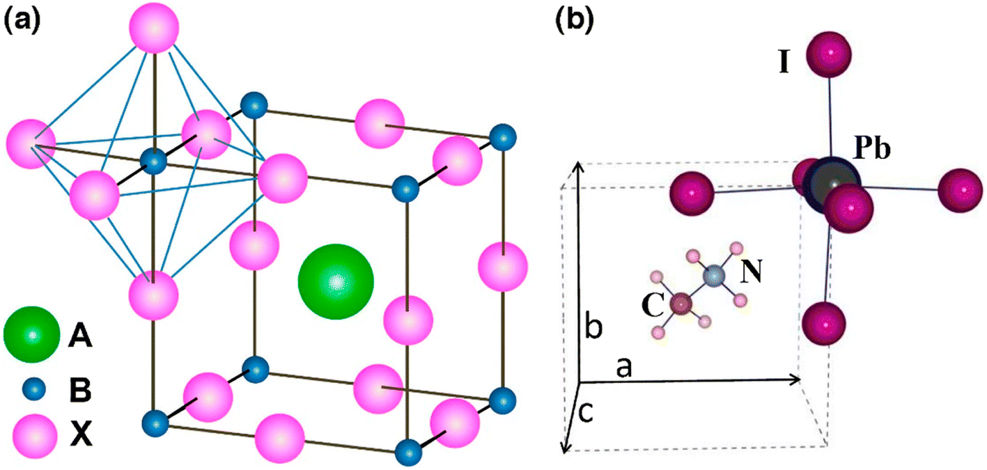 | ||
| Fig. 1 (a) ABX3 perovskite construction presenting BX6 octahedral and bigger A cations engaged in the cuboctahedral place. (b) The element cell of cubic MAPbI3 perovskite (reproduced with permission from ref. 25, copyright 2015 Elsevier). | ||
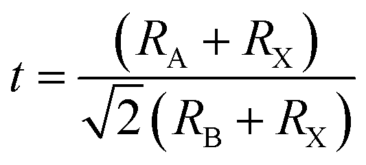
In order to enumerate the stability and structure of perovskites, two vital constraints are the octahedral factor (μ) and tolerance factor (t)26 The tolerance factor is defined as a ratio of the bond lengths of A–X and B–X in a perfect solid-sphere model. Scientifically, it can be written as:
 | ||
| Fig. 2 Tolerance factor (t) and octahedral factor (μ) calculated values for perovskites (reproduced with permission from ref. 28, copyright 2014 NPG). | ||
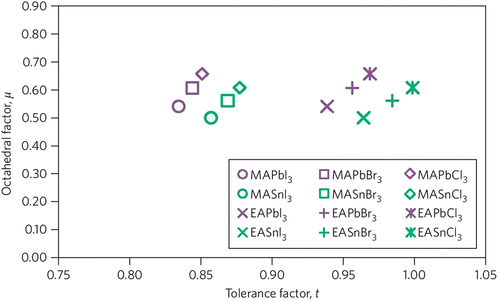
1.2. Working mechanism of PSCS
The working principles of OSCs and dye-sensitized solar cells (DSSCs) help in knowing the operation of PSCs. A representative diagram of the working mechanism of PSCs is shown in (Fig. 3). PSCs employ perovskite-structured light absorbers for photovoltaic motion; similarly, DSSCs use the dye/semiconductor boundary for light gathering. The photovoltaic structure has three key operative stages: | ||
| Fig. 3 Band plan and working mechanism of PSCs (reproduced with permission from ref. 32, copyright 2017 Elsevier). | ||
(1) Photon absorption trailed by the generation of free charge
(2) Transport of charge
(3) Extraction of charge
When sunlight strikes a PSC, the perovskite material grips light, excitons are formed, and charge transporters (electrons and holes) are formed upon exciton parting. Exciton parting occurs at the boundary between the charge-transporting layer and perovskite film. After the electron is detached from the hole and inserted into the electron transporting layer (ETL), it travels to the anode usually made of fluorine-doped tin oxide (FTO) glass. Instantaneously, the hole is inserted into the HTL and afterward travels to the cathode (typically a metal).29 The holes and electrons are collected by counter and working electrodes, separately and moved to the outward circuit to generate current.30,31
1.3. Physical design of PSCs
Cell formation is a basic feature for assessing the complete role of solar cells. PSCs can be organized as usual (n–i–p) and inverted (p–i–n) constructions relying on which carrier (electron/hole) material is existing on the external side of the cell and that is met by incident light first. Further, these two assemblies can be categories as mesoscopic and planar cells. The perovskite devices based on mesoscopic construction include a mesoporous layer while the planar structure contains all planar films. Perovskite devices without holes and electron transporting layers have also been verified. In short, six categories of PSCs have been considered by several researchers so far: the mesoscopic n–i–p arrangement, planar n–i–p arrangement, planar p–i–n arrangement, mesoscopic p–i–n conformation, ETL-free structure, and HTL-free structure.1.4. Classical n–i–p and inverted p–i–n formations
The regular n–i–p mesostructured construction was the first ever plan of perovskite devices to be verified, where the light-capturing dye was substituted with lead halide perovskite semiconductor materials in old-style DSSC-type cells.32 The cells start with a transparent glass cathode trailed by the electron-transporting material (ETM).33 The assembly is then covered using a mesostructured metal oxide comprising a perovskite absorber, trailed by the hole transport material (HTM), and topped with a metallic anode (Fig. 4a). This early progress for perovskite devices formed a significant area of research for the photovoltaic community and therefore directed to the growth of other perovskite device arrangements (Fig. 4b–d). It is imaginable to attain better performance in the absence of mesoporous film by wisely monitoring the boundaries between the various layers that construct the planner PSC.34,35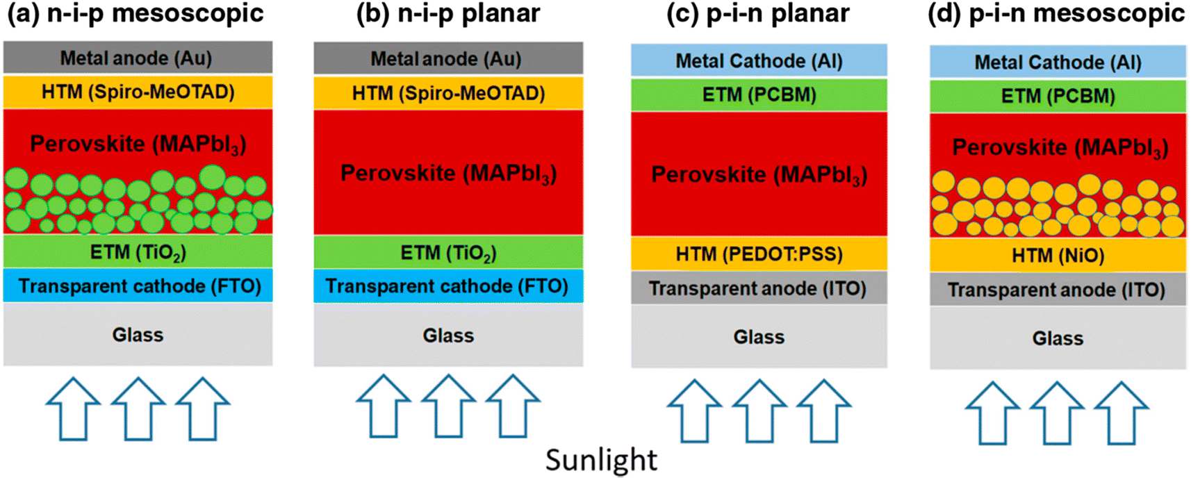 | ||
| Fig. 4 Diagram displaying the four-layered assemblies of PSCs (a) n–i–p mesoscopic, (b) n–i–p planar, (c) p–i–n planar, and (d) p–i–n mesostructured (reproduced with permission from ref. 36, copyright 2016 SPIE). | ||
Using the identical materials and method, a planar n–i–p PSC displays improved open-circuit voltage (VOC) and short-circuit current density (JSC) compared to mesostructured PSCs, but, the planar devices showed more J–V hysteresis, which was a big question about the testified efficiencies.36 The depth and grain of this buffer film mainly affect the J–V hysteresis curves.37 Kim et al. detected that the negligible hysteresis in J–V curves was found by reducing the capacitance, which was accomplished by substituting Spiro-OMeTAD with poly(3,4-ethylenedioxythiophene)-poly(styrene sulfonate) (PEDOT:PSS).38 Though, the behavior of J–V hysteresis also relies on the scan direction of voltage, scan range, and rate.39 In order to overcome this issue, a slim mesoporous buffer coating was combined inside the planar n–i–p PSC assembly. Though mesoporous PSC displayed improved performance compared to planar devices, it is essential to produce a slim mesoporous film (less than 300 nm). Moreover, the planar device could be made-up using a low-temperature method in contrast with the mesostructured cells. However, the improved formation of the perovskite-absorbing film is essential.40,41
The p–i–n structured-based perovskite devices are based on organic solar cells.42 In this case, the HTM layer is first coated before the ETL is formed. It was revealed that perovskites are proficient enough to transfer the holes themselves,43 which was helpful to introduce the initial planar hetero-junction PSC having an inverted operational assembly.36 With this development, the inverted p–i–n conformation has extended the possibilities to discover further selective layers from organic to inorganic materials. Planar p–i–n PSC facilitates their processing at low-temperature, slight J–V hysteresis having a high PCE of 18%.44,45 The device arrangement of the inverted mesoscopic and planar p–i–n PSCs is revealed in Fig. 4c and d.
In addition, inexpensive HTM-free carbon-based PSCs (C-PSCs) have attracted significant attention because of their superior stability, and ease of fabrication, which make them highly suitable to replace HTL and metal electrodes. Zhiliang et al., first described high-temperature treated mesostructured support designed (TiO2/ZrO2/C) HTL-free C-PSCs,226 which confirmed effectual charge transference at perovskite/carbon and TiO2/perovskite boundaries. With the hard work of scientists, the PCE of these devices has surpassed 17%.227 In the recent past, planar-designed HTL-free C-PSCs utilized low-temperature treated tin oxide (SnO2) (150 °C) to substitute TiO2 as an ETL and have been established as an alternate cell assembly,228 though, the inadequate interfacial charge transfer strictly bounds the performance of these devices. Thus, interfacial charge transfer strengthening is vital for high-performance planar-organized HTL-free C-PSCs. Many efforts have been put into advancing the interaction at the perovskite/carbon boundary using either inserting carbon nanotubes as bonds or presenting nanosized carbon materials to block the openings at the perovskite/carbon border.229,230
1.5. ETL-free perovskite devices
A dense layer of metal oxide on the surface of transparent conductive oxide (TCO) is constantly essential for classical planar PSCs since it aids to attain high VOC and overall device performance. However, Huang et al. established a surface amendment method by applying a cesium salt solution to amend the surface of indium-tin-oxide (ITO) or to adjust the energy level arrangement at the interface, which directed to a PCE of 15.1%.46 Further, compact layer-free perovskite devices were developed by the researchers, which showed 13.5% PCE by straight coating the perovskite absorber layer onto the ITO with the help of a sequential layer deposition technique, indicating that the presence of ETL is not essential to gain better device performances.47 Ke et al. also recommended that a TiO2 ETL may not be a perfect interfacial material after producing an effective ETL-free PSC producing a PCE of 14.14% rightly coated on an FTO glass substrate using a one-step method with no hole-blocking films.48 The dense ETM layer-free planar PSC construction is displayed in Fig. 5. Other researchers have also shown that the compact layer-free style can produce admirable cell efficiency when made using various layer-processing procedures.49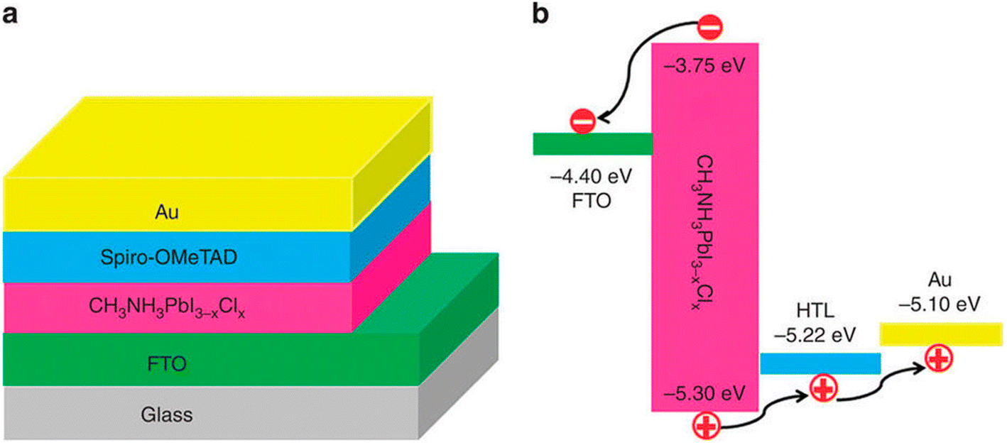 | ||
| Fig. 5 (a) Symbolic representation of the ETL-free planar PSC arrangement and (b) energy level illustration of the planar PSC presenting gathering and parting of photo-generated electrons and holes in the absence of ETL (reproduced with permission from ref. 48, copyright 2015 NPG). | ||
1.6. HTL-free PSCs
Though numerous hole transport materials (HTMs) were introduced with decent consequences (namely inorganic compounds, polymers, and small molecules), HTM-free PSC designs are a modest cell arrangement. This increasing importance is due to the testified highly effective PSCs comprising exclusive HTMs such as fullerenes, which meaningfully surge the manufacturing cost of these cells. As previously stated, perovskite materials expressed excellent semiconducting characteristics such as ambipolar behavior and longer lifetimes of charge transport, which eliminated the use of HTL.50 For the first time ever, Etgar et al. suggested the fruitful manufacturing of HTL-free mesoscopic PSCs, demonstrating that MAPbI3 itself worked both as a hole conductor and a light harvester.44,51,52 The value of the perovskite absorber layer and the additional care of the performance of HTM-free PSCs. The simplest HTL-free PSC assembly is displayed in Fig. 6. The diverse cell conformations enlighten the choice of charge-transport (HTM and ETM) and charge-gathering materials (anode and cathode).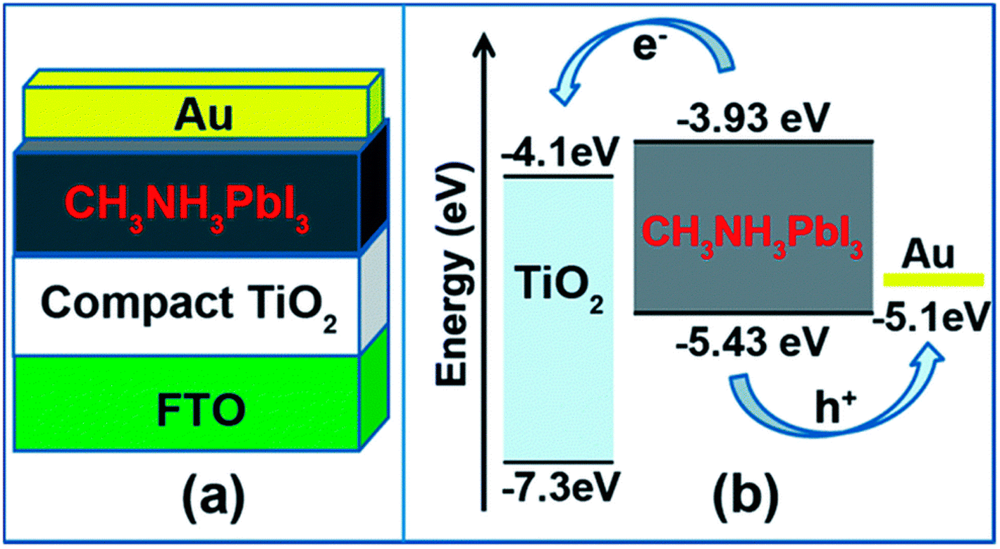 | ||
| Fig. 6 Simplified model of the (a) construction and (b) energy level arrangement of the planar HTL-free PSCs (reproduced with permission from ref. 53, copyright 2016 Elsevier). | ||
2. Types of materials for PSCs
2.1. Monovalent cation mixing/substitution
The alteration of monovalent cations can expand the efficiency of PSCs in a particular way. Though methylammonium lead iodide (MAPbI3) is typically used as a light-absorbing material in perovskite devices; there is a continuing quest for other novel materials to substitute methylammonium (MA) in MAPbI3 owing to their poor stability and insignificant band gap.54 The optimum band gap in the case of single junction solar cells lies between 1.1 and 1.4 eV though the published band gaps of MAPbI3 are between 1.50 and 1.61 eV.55 Replacing the MA ion with a little bigger organic formamidinium (FA) ion consequences in a cubic assembly with a rather larger lattice and therefore a minor reduction in the band gap from 1.59 eV for MAPbI3 to 1.45–1.52 eV for FAPbI3 that permits collection of more light.56 Similarly, Hanusch et al. disclosed that FAPbI3 is thermally steadier than both MAPbI3 and methylammonium lead bromide (MAPbBr3), which sturdily proves the results that a bigger cation at the A site in ABX3 assembly might support the perovskite structure in a better way.57 Nevertheless, FAPbI3 also has stability due to its sensitivity towards the contamination of solvent and humidity, since it results in photo-inactive, non-perovskite hexagonal δ-phase (yellow phase) or photoactive perovskite α-phase (black phase).58,59Fig. 7 displays the tolerance factor of steady alkali metals A = Rb, K, Li, Cs, and Na and two extra mutual monovalent cations MA and FA. The graphs of the tolerance factor represent that MAPbI3, FAPbI3, and CsPbI3 lie in the range of 0.8 to 1.0 having a black phase. It was also observed that on heating CsPbI3, the layer goes black while RbPbI3 stays yellow. Therefore, in spite of its outstanding oxidation constancy, alone Rb may not be utilized in perovskite devices.60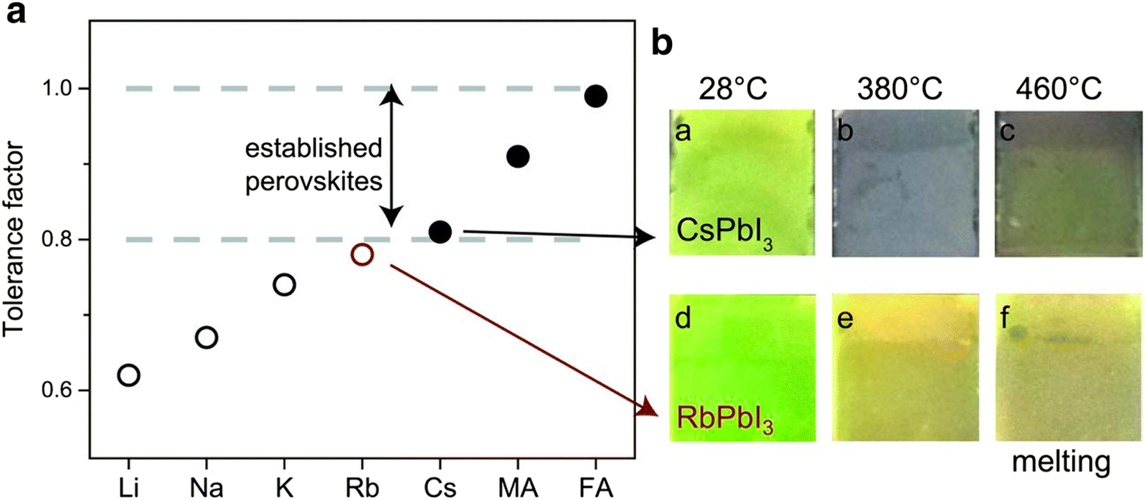 | ||
| Fig. 7 Tolerance factor and perovskite pictures at diverse temperatures. The tolerance factor of perovskite between 0.8 to 1.0 displays a photoactive black stage (solid circles) whereas a tolerance factor below 0.8 shows a non-photoactive stage (open circles). Reproduced with permission from ref. 61. Copyright 2016 AAAS. | ||
In the recent past, Prochowicz et al. verified that the inclusion of 25 molar% of MAI to the reaction blend may steady the black stage of FAPbI3, and they achieved a PCE of 14.98% having a JSC of 23.7 mA cm−2.49,62 Choi et al. described that doping the MAPbI3 structure with 10% Cs gave rise to a 40% improvement in device productivity due to better morphology and enhanced light absorption.63 Lee et al. established that moisture and photo-stability of FA0.9Cs0.1PbI3 were considerably enhanced compared to pristine FAPbI3.54,64 Keeping in mind the target of high device performance and long-term stability, Cs was adopted to explore more complex cation combinations, i.e., Cs/MA/FA. The triple-cation (Cs/MA/FA)-based PSCs have duplicability and thermal constancy than MA/FA double-cation perovskites.60 The addition of Cs into MA/FA cation blends aids to disintegrate the cubic PbI2 and photo-sluggish hexagonal δ-phase of FAPbI3 totally. Additionally, the addition of Cs in different quantities (5%, 10%, 15%) caused a blue shift of 10 nm for the photoluminescence (PL) and absorption spectra along with a smaller cationic radius, creating the black perovskite stage extra intrinsically steady even at room temperature.60 These findings are displayed in Fig. 8.
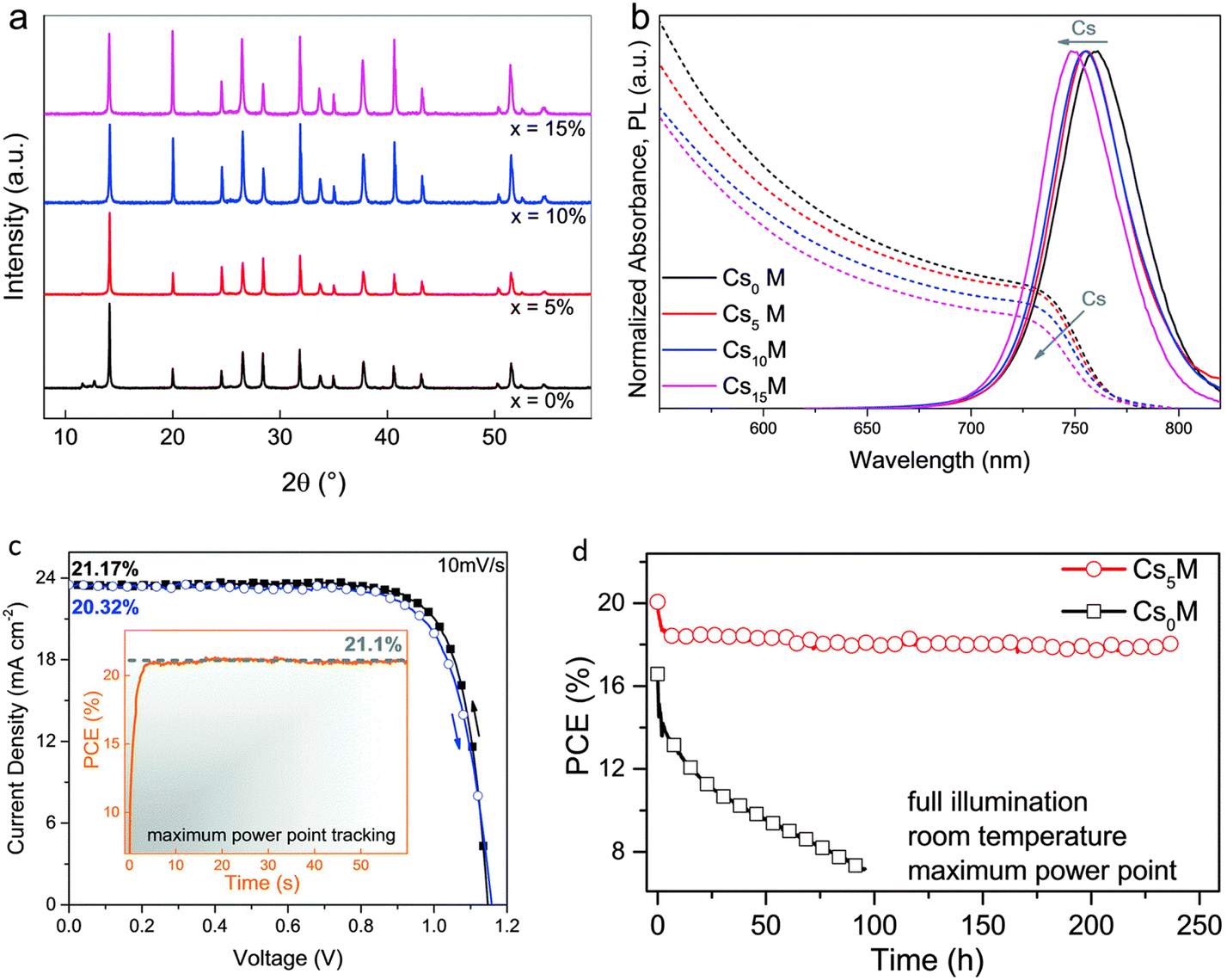 | ||
| Fig. 8 Consequences of Cs accumulation in MA/FA cation blends; (a) XRD and (b) optical findings (c) current–voltage (J–V) and (d) stability properties of CsxMAFA complexes (reproduced with permission from ref. 60. Copyright 2017 RSC). | ||
In order to discover other monovalent cations, Saliba et al. fused Rb into a photoactive perovskite phase by introducing various cation (RbCsMAFA) designs. Alkali metals were chosen as the monovalent cations owing to their intrinsic stability in the oxidation environment. They also recognized various combinations of cationic perovskites such as RbCsFA, RbCsMAFA, RbFA, and RbMAFA producing reliable device efficiency as compared to formerly discovered cationic mixture-based perovskites such as CsMAFA and CsFA. These findings unlocked the access to utilize other organic–inorganic cation mixtures together with further inorganic cations in perovskite devices.61
2.2. Halide substitution
The substitution or replacement of halogen ions may adjust the optoelectronic characteristics of perovskite materials. In the MAPbI3 assembly, iodine(I) can be replaced with both bromine and chlorine, and huge single crystals were formed using all three lead halide perovskites; MAPbI3, MAPbCl3, and MAPbBr3 (Fig. 9). Liu et al. evaluated the optical characteristics (PL spectra, band gap, and absorption spectra) of MAPbX3 (X = Cl, Br, I) as a function of the halogen anions, as displayed in Fig. 10. A sudden change in the absorbance was observed after the halide was replaced with Br, Cl, and I. As the ionic radius of the halide increases, the band gap energy reduces, such as for a single crystal, the band gap is 2.97, 2.24, and 1.53 eV for the Cl, Br, and I perovskite, respectively. Furthermore, the reduced PL peak intensities compared to the absorption onsets make it ideal for them to be used in solar cells.64,65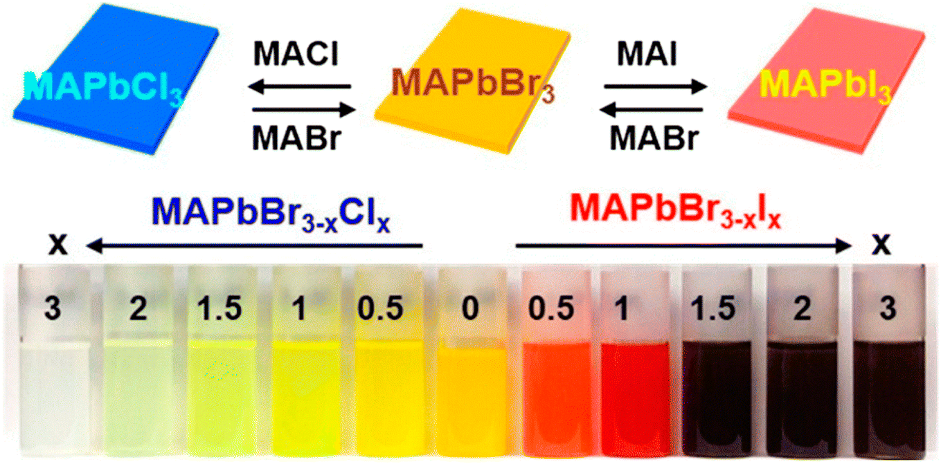 | ||
| Fig. 9 Snapshots of halide replacement/mixing in the perovskite assembly (reproduced with permission from ref. 66, copyright 2014 ACS). | ||
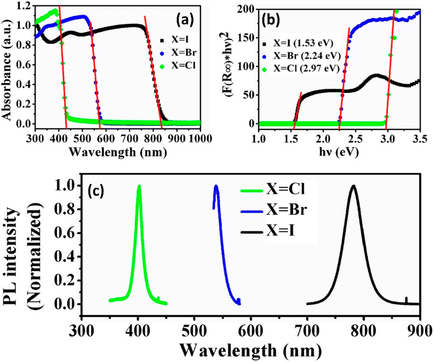 | ||
| Fig. 10 Influence of halide replacement on the optoelectronic characteristics of perovskites: (a) absorption spectrum, (b) band gap, and (c) photoluminescence spectrum (reproduced with permission from ref. 70, copyright 2014 Elsevier). | ||
MAPbBr3 and MAPbI3 are appropriate for tandem devices as well as for single-band gap absorbers, while MAPbCl3 is more beneficial for light-emitting applications.67 Though, for the perovskite devices the halide mixing offers extra benefits in terms of stability, band gap adjustment, and improved carrier transport. Lee et al. reported that the blend of halide perovskite MAPb(I1−xClx)3 offers stability benefits over MAPbI3 while synthesizing in the air.68 Noh et al. established that mingling 20–29% Br into MAPbI3 meaningfully improved the stability of the perovskite devices while sustaining the cell's performance.69
Additionally, greater electron–hole diffusion lengths were observed for MAPb(I1−xClx)3 compared to MAPbI3, whereas the MAPb(I1−xBrx)3 and MAPb(Br1−xClx)3 showed fewer rates of carrier recombination and improved carrier movement.70–82 Though, it is difficult to produce mixed (I, Cl) perovskite less than 625 K, whereas it is easy to synthesize mixed (Br, Cl) and (I, Br) perovskites at room temperature.83–90 Jeon et al. showed that (FAPbI3)0.85 (MAPbBr3)0.15 has numerous benefits compared to blends such as FAPbI3, MAPbI3, and MAPb(I0.85Br0.15)3.58 Jacobsson et al. exhibited that a minor change in the chemical structure will have a prominent effect on the perovskite materials characteristics and eventually enhance the cell performance in case of a double-cation double halide mixed PSCs.71,91–98 Moreover, as discussed already in the previous segments, scholars are combining more cations (triple, quadruple) with the mixed halide to obtain enhanced stability and performance.61,99–112
3. Electron-transporting materials
ETL, is occasionally called an electron collection or extraction layer, where electrons are inserted from the perovskite absorber layer, moved over the electron transporting materials (ETM), and lastly together with the metal electrode. ETL can be substituted with a fused photoelectrode to enhance the charge-gathering productivity by dropping the series resistance.113,114 Furthermore, ETLs composed of one-dimensional nanostructures can provide rapid charge transport in solar cells.A schematic illustration of PSC architecture is shown in Fig. 11. The universal arrangement of PSCs classically comprises a light-absorbing layer that is reversed between ETL, along with FTO, and metal electrodes are assisted as a glass substrate and back electrode, separately.115–117 The detailed working and charge transport mechanisms are defined in Fig. 11a–c. The hole and electron shadowing in the device construction causes a more recombination rate. In a planar heterojunction PSC, the performance can be prominently enhanced by creating suitable pathways for both holes and electrons.118,119.
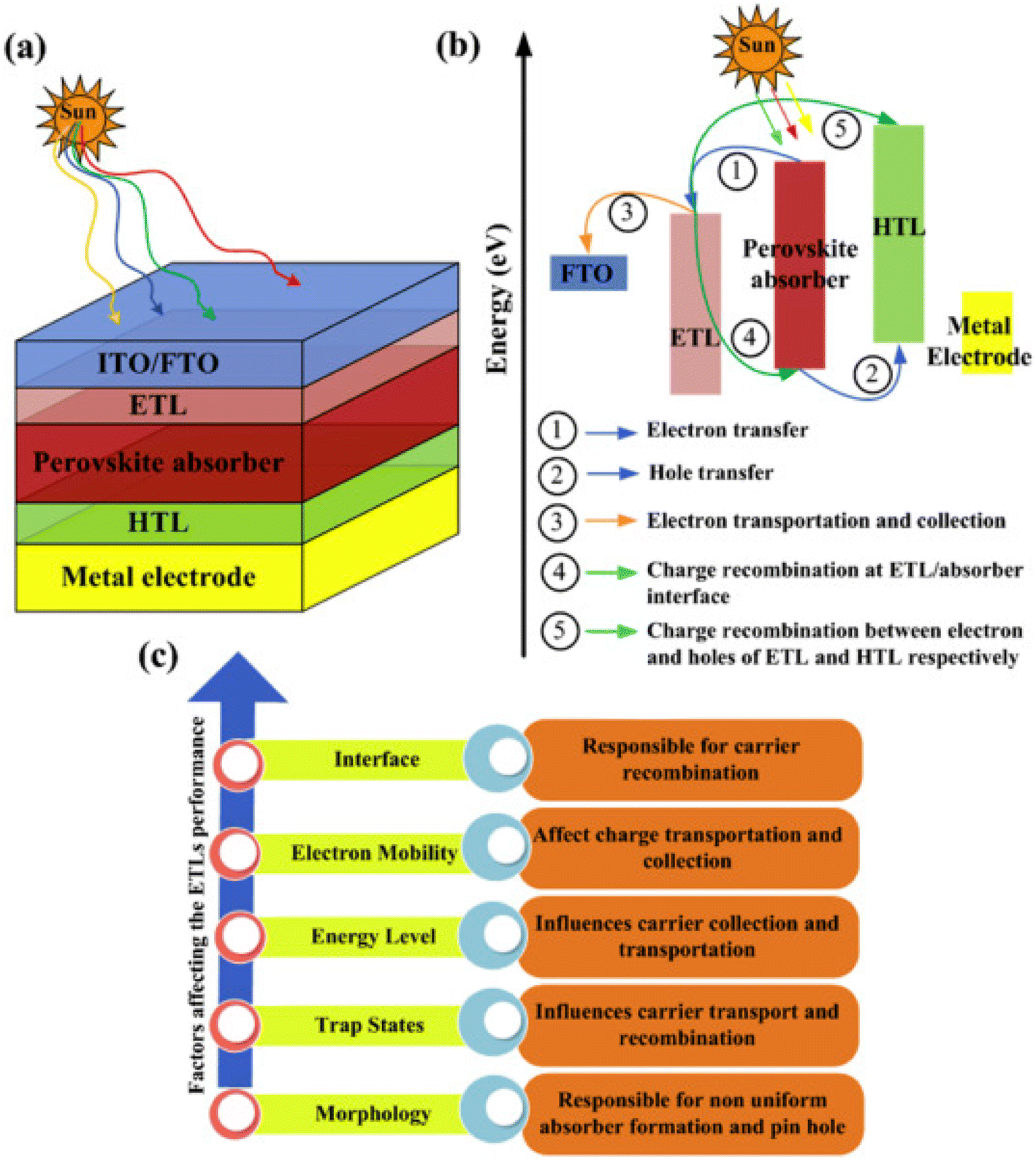 | ||
| Fig. 11 (a) PSC assembly. (b) Graphic depiction of working and charge transference routes in ETLs of PSCs. (c) Factors influencing the ETL efficiency in PSCs (reproduced with permission from ref. 114. Copyright 2022 Elsevier). | ||
ETLs are films having a conduction band minimum (CBM) that must be inferior to that of a perovskite light absorber.120–122 The perovskite devices investigations initiated with TiO2 as an ETL back in 2009, when a solar device was considered using a Pt-covered FTO as a glass substrate and CH3NH3PbBr3 as a light absorber, respectively.12 Exploration in PSCs explicitly emphasizes low-temperature layers deposition, which introduces various better other ETLs, such as CdS, In2O3, Fe2O3, In2S3, Nb2O5, Zn2SO4, and IGZO have also been extensively used in PSCs.123–125 Indeed, organic ETLs have also revealed their occurrence in PSCs with lesser recombination rates and hysteresis.126,127 Additionally, diverse approaches such as multilayer research of ETL, thickness variation and alteration in dopant concentration, and growth of novel nanostructures, along with surface and interfacial engineering methods were approved for highly stable and high-performance PSCs.128,129 In order to select a proper ETL, the following things should be considered. The material should avoid the chemical reaction with adjacent light-absorbing material and electrodes. Better and dense morphology of the films is needed to restrict the drip from the films and pinhole. The widely used ETLs in PSCs are TiO2, SnO2, and CdS.130–132
3.1 Inorganic electron transporting layers
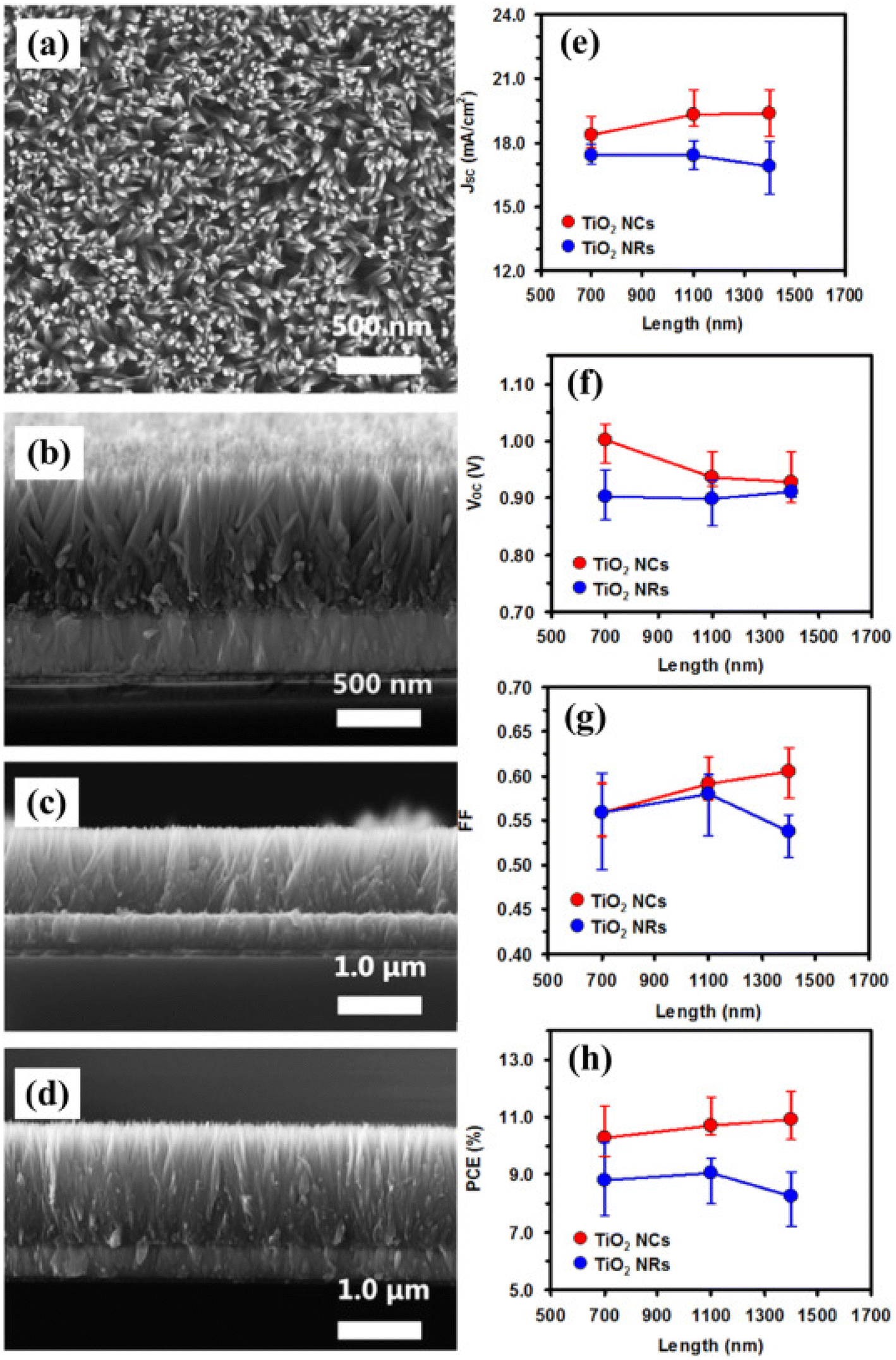 | ||
| Fig. 12 (a) Top view of nanocones and (b) side view of SEM image of TiO2 nanocones grown over FTO glass substrate (a and b) with 700 nm, (c) 1100 nm, (d) 1400 nm, TiO2 nanocones. Comparative works of both TiO2 nanocones and nanorods for 16 devices having various physical parameters (e) JSC, (f) VOC, (g) FF, and (h) PCE of PSCs with respect to length (reproduced with permission from ref. 139. Copyright 2015 Elsevier). | ||
Many studies also showed that the device efficiency can be enhanced after doping metal cations in TiO2 ETL, which improves the charge collection and light-capturing ability.136 To decrease the carrier buildup at boundaries and improve the charge transport in current years 2D materials and graphene have been also explored. The architecture is fabricated of four devices with the following ETLs.140
• graphene mesostructured TiO2 (ETL1) + mesostructured TiO2 (ETL2)
• mesostructured TiO2 + graphene oxide (GO) having Li interlayer (ETL3)
• graphene + mesostructured TiO2 + GO as Li interlayer (ETL4)
For the ETL4 sample, the crystalline quality is much superior compared to other ETLs.
The enhancement in electron gathering and transport can be attained by:
• interaction between the ETL and light-gathering film should be proper
• choice of TCO
• metal cations should be tailoring ETLs
• By introducing nanostructured electron transfer material
Furthermore, to improve the performance and reduce the recombination losses Mahmood et al. introduced a concept of double-layer ZnO nano-structured.145 The hydrothermal method by which a double-layer ZnO nanostructure is formed causes the growth of nanorods on ZnO sheets. The density of ZnO nanorods was controlled by varying ZnO solution concentration from 0.02 M to 0.06 M. For 0.02 M to 0.06 M J–V curve and EQE spectra are revealed in Fig. 13a and b. As the concentration increased to 0.06 M, the JSC value increased. Similarly, the PCE enhanced from 6.98% to 10.35% and VOC improved from 0.83 V to 0.928 V.
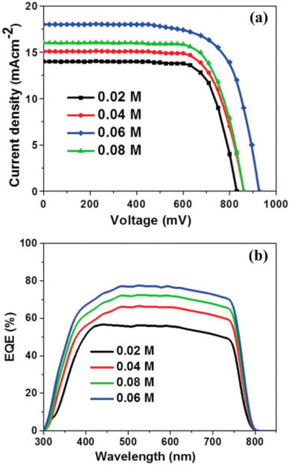 | ||
| Fig. 13 (a) J–V, and (b) EQE properties of PSCs as a function of precursor concentration 0.02 M, 0.04 M, 0.08 M, 0.06 M (reproduced with permission from ref. 145. Copyright 2014 RSC). | ||
Wang et al. using indium zinc oxide (IZO) as ETL achieved a PCE of 16.25% with insignificant hysteresis.146 Cao et al. fabricated the hysteresis-less and constant PSC by depositing a thin film of MgO over the ZnO surface (Fig. 14).147
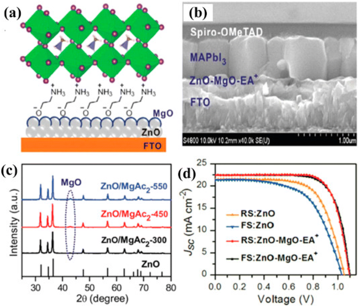 | ||
| Fig. 14 (a) Graphic depiction of altered planar perovskite thin-film assembly with ZnO-MgO-EA+. (b) SEM image exhibiting the side view of the device. (c) XRD arrangement of the precursor solution having diverse temperature environments. (d) JSC–V curves. (Reproduced with permission from ref. 147, Copyright 2018 Wiley-VCH). | ||
The interfacial approach was adopted to improve the stability and photovoltaic characteristics of PSCs.
To date, the main concern for PSCs is long-term stability. This aspect was not explained much for SnO2 ETL-based PSC devices. Choi et al. for the construction of thermally steady PSCs, fused 3-(1-pyridinio)-1-propanesulfonate zwitterionic composite in SnO2 ETL. The zwitterions compound has some advantages150
• It enhances the transportation ability to ETL from the perovskite absorber and also the electron collection ability
• Back transport of electrons from the collection film to the perovskite light absorber prevents the formation of an interfacial dipole
• Charge extraction improvement and enhancement of built-in potential is by the incorporation of zwitterion
• The positively charged atoms of zwitterion enrich the device's stability
Yoo et al. for managing the charge transport in PSCs reported an innovative approach. Initially, they established SnO2 as ETL.151 Then, between the interfaces, and bulk passivation method was implemented that enhanced the film quality. They divided the growth variation into stage B and stage A. Stage A is further divided into three parts A-i having pH 1 with acidic nature, A-ii having pH 1.5, and stage A-iii having pH 3. Stage B showed the ultimate response with diverse morphology at extreme pH 6, Fig. 15 represents the growth device with the presentation of various stages.
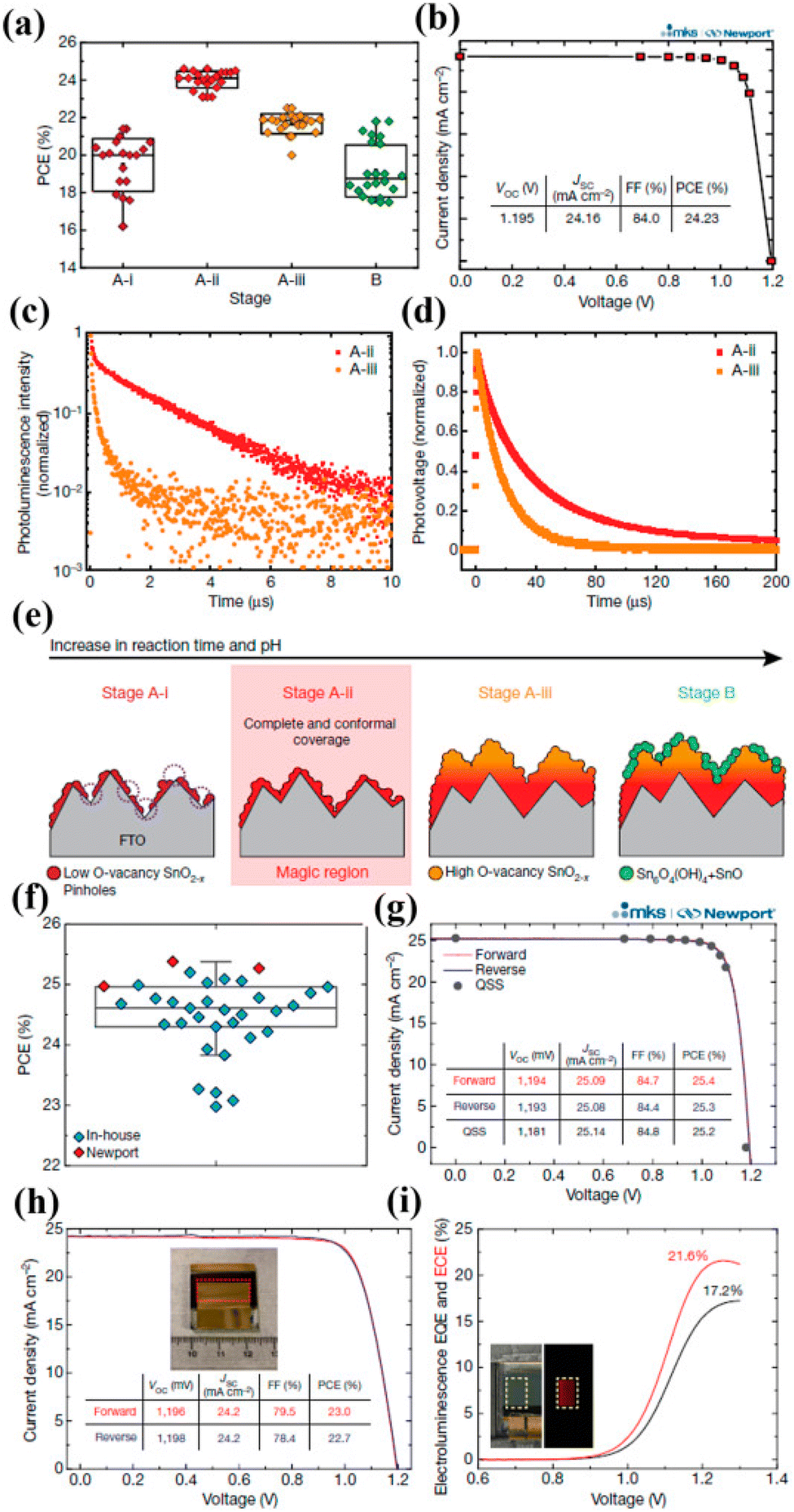 | ||
| Fig. 15 (a) The difference in PCE of PSCs together with alteration in SnO2 preparation phases. (b) Quasi-steady-state current density vs. voltage characteristic for stages A-ii. (c) Time-resolved photoluminescence study for perovskite absorber set for the stage A-ii (red trace), stage A-iii (orange trace) of SnO2 ETL. (d) Transient photovoltage study for stage A-ii and stage A-iii, SnO2-based PSCs. (e) The development stage of SnO2 ETL. (f) Statistical spreading depiction in box-and-whisker plots for established PSCs. (g) J–V curves of the produced PSCs obtained at Newport. (h) J–V curve displaying supreme PCE of 23% under the active area of 0.984 cm2. (i) Electroluminescence EQE and ECE findings of PSC under forwarding bias (reproduced with permission from ref. 151. Copyright 2021 NPG). | ||
3.2. Organic ETLs
Intense care is needed for the processing of layer development at low-temperature especially in PSCs. Yoon et al. produced vacuum-formed C60 electron selective film, treated at room temperature. Variation in device performance was observed as a function of bathocuproine (BCP) addition. The devices with BCP interlayer showed enhanced output due to the significant electron extraction characteristics. Hysteresis-less devices were also fabricated by using C60 ETL on polyethylene naphthalate (PEN) substrates showing high device performance.153
The developed device under 1-sun illumination showed a PCE of 18.2% with a small hysteresis current. The commercialization of these ETLs hindered due to the higher cost of the fullerenes derivative. Xu et al. studied the mixture of C60 and C70 as the pristine fullerene mixture (FM). The solubility was improved due to enhanced configurational entropy up to 52.9 g L−1, which through the spin-coating technique showed a reduction in the crystallization rate of FM.154 The PEC of the developed device with FM ETL was 16.9%. Pascual et al. deposited a C70 layer on an FTO glass substrate. The device delivered a PCE of 13.6% made-up of cell arrangement of FTO/MAPbI3:C70/Spiro-OMeTAD/Au.155
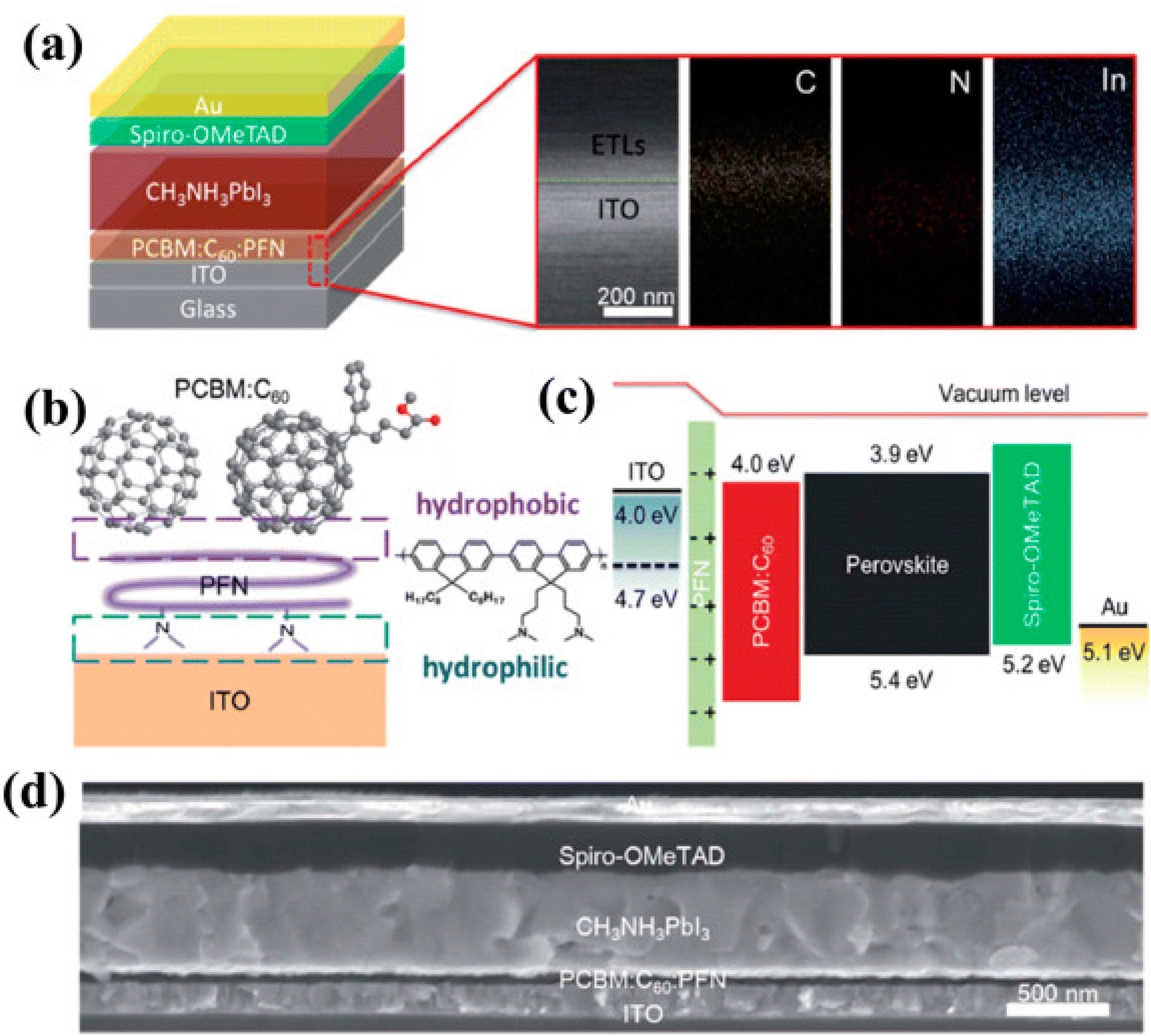 | ||
| Fig. 16 (a) Illustrative depiction of the produced thin-film assembly and SEM image with EDS plotting of the cross-section of ITO/PCBM:C60:PFN (approx 120 nm). (b) Symbolic drawing of vertical phase parting in the ternary PCBM:C60:PFN and molecular structure of PFN. (c) Energy figure, and (d) SEM image showing the side view of the established device (reproduced with permission from ref. 159. Copyright 2018 RSC). | ||
PSCs having decent transparency has also gained much attraction. Keeping this in mind, Li et al. fabricated a PSC via a low-temperature-based film formation technique with PCBM ETLs.161 The PSCs construction using classical PCBM is revealed in Fig. 17a–c displays the device construction explaining the absorber grain boundaries and the development of PCBM dispersed inside the ETL film. Top view of SEM and cross-sectional TEM image Fig. 19d and e show the development of PCBM-fused PSCs. Afterward, it was melted in chlorobenzene the evolution of PCBM-supported ETL, produced an even and pinhole-free surface.
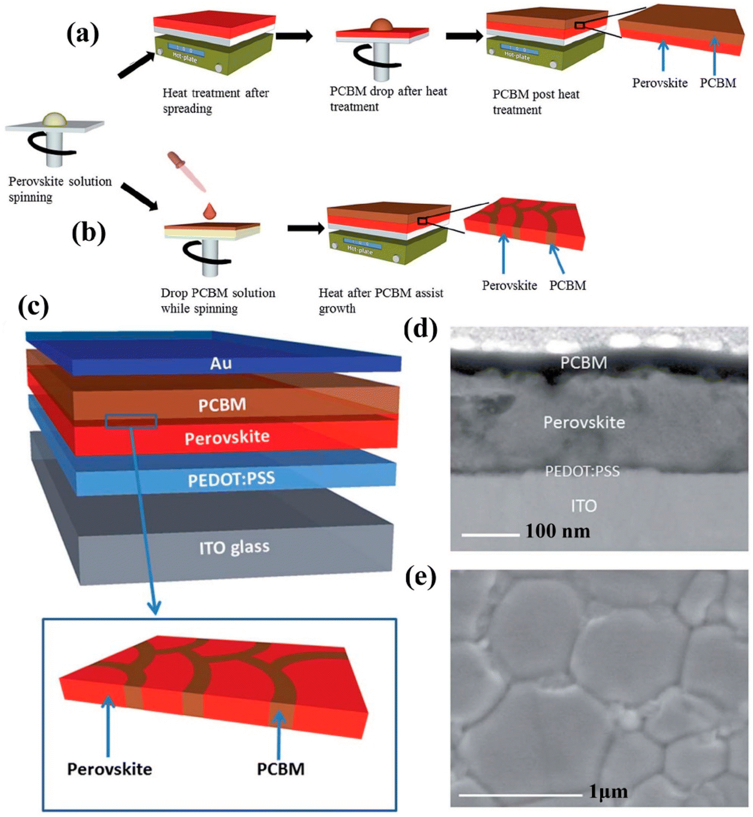 | ||
| Fig. 17 Symbolic depiction of the development of PSCs, (a) using classic PCBM preparation route, (b) PCBM-supported preparation route. (c) Device construction of PSC using hybrid PCBM – absorber film, (d) cross-section TEM image of established PSC, and (e) top-view SEM figure of as-prepared perovskite absorber produced using chlorobenzene (CB)-supported method.160 Three different PSCs comprising of single perovskite layer, perovskite/PCBM bilayer, and polymerized formula designed by Zhong et al. using temperature-based chronoamperometric examination and by dropping ionic motion the enhanced activation energy was noticed (reproduced with permission from ref. 161. Copyright 2020 Wiley-VCH). | ||
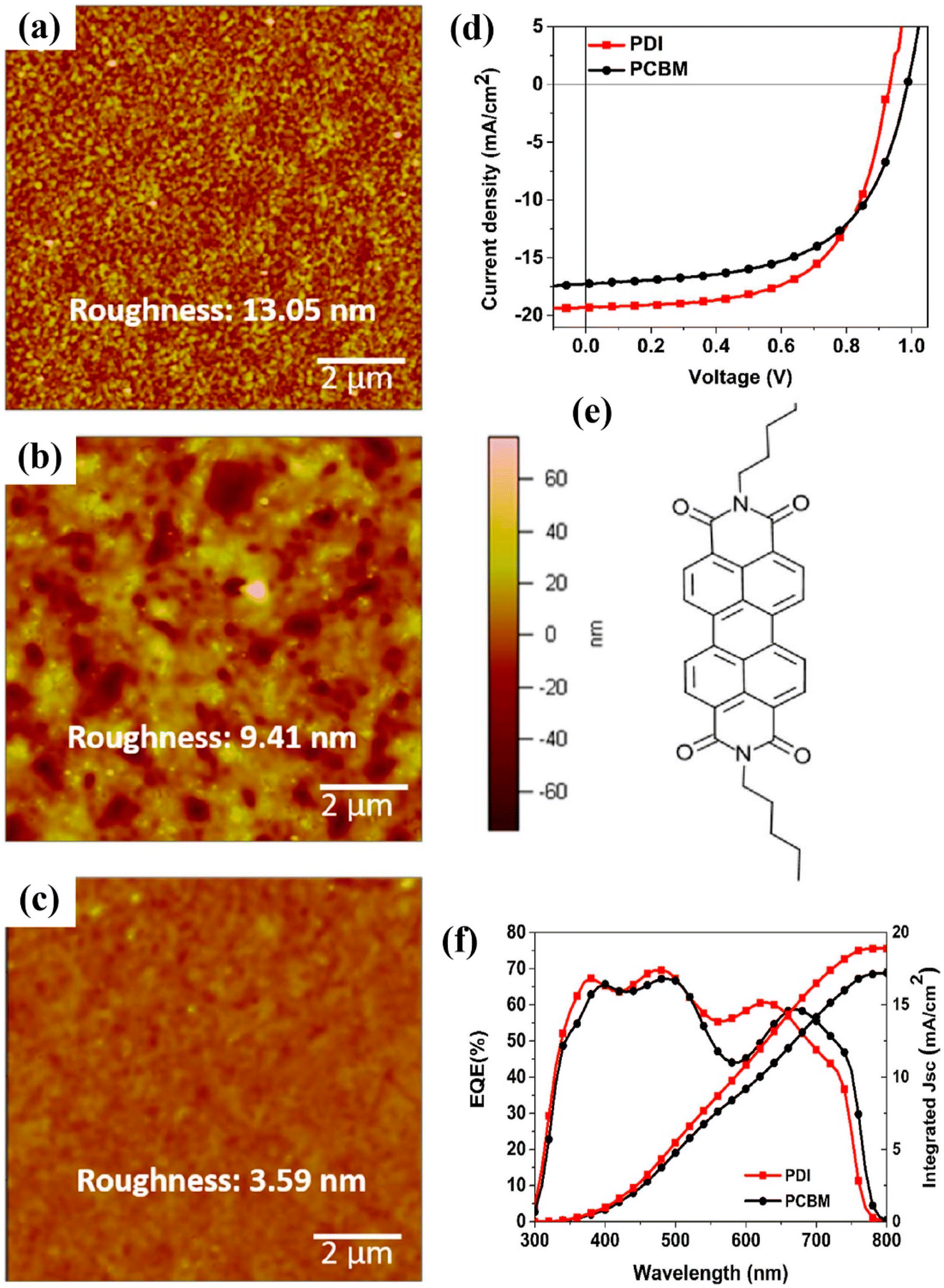 | ||
| Fig. 18 AFM pictures of perovskite absorber (CH3NH3PbI3−xBrx) (a) prepared on PEDOT:PSS film, (b) after fabrication of PCBM, and (c) PDI film on PEDOT:PSS/perovskite thin layer. (d) J–V curves, (e) PDI molecular assembly, and (f) EQE-wavelength findings for both PCBM and PDI ETL-based PSCs (reproduced with permission from ref. 164. Copyright 2017 Elsevier). | ||
The development of ETM is vital for refining the performance of PSCs. Both inorganic and organic material-based ETMs can be utilized in PSCs; characteristically, inorganic ETLs are widely used in conventional cell construction while organic materials are utilized in inverted devices.165 The energy stages of the most commonly used inorganic and organic ETLs utilized in PSCs are shown in Fig. 19 and 20, respectively.166
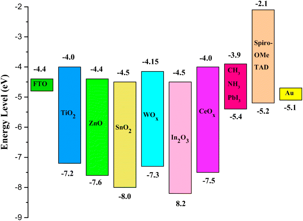 | ||
| Fig. 19 Energy zones of diverse materials used as inorganic ETM in different films of PSCs (reproduced with permission from ref. 166. Copyright 2018 Springer). | ||
 | ||
| Fig. 20 Energy zones of diverse materials used as organic ETM in different films of PSCs (reproduced with permission from ref. 166. Copyright 2018 Springer). | ||
Currently, owing to prominent electron-transport characteristics, TiO2 is the widely used ETL in the classical n–i–p PSC construction.167 However, the high sintering temperature is needed to attain the desired crystallinity, which makes it unsuitable to use in PSCs in order to achieve high performance.168–173 Therefore, the need for a low-temperature method for the fabrication of TiO2 film is dynamic these days. Coning et al. established a sol–gel procedure to prepare TiO2 nanoparticulate ETL and obtain a PCE of 13.6%.169 Yella et al. also recognized a low-temperature production method employing nanocrystalline rutile TiO2 formed using a chemical bath deposition technique, and they achieved a PCE of 13.7%.174 Wu et al. established the utilization of low-temperature (<100 °C) solution-based TiOx ETL in PSCs and achieved a high PCE of 17.6%.172 In the case of UV light, it has been initiated that TiO2 ETL-based devices have low stability, which could be a test towards the industrialization of TiO2-based PSCs.
Jiang et al. introduced a clear luminescent down-converting film of Eu-complex (Eu-4,7-diphenyl-1, 10-phenanthroline) to improve the light employment and initiate that integrating an Eu-complex film aided to improve 11.8% JSC and 15.3% PCE caused by re-emitting UV light (300–380 nm) in the visible region unlike the uncovered any down alteration film.175,176 Furthermore, the electron injection amount from the photoactive perovskite absorber film to the TiO2 ETL is very rapid, this is balanced rather by high electron recombination rates due to low electron movement.177 Therefore, there is much attention on discovering other inorganic ETLs to improve the stability and performance of PSCs.178 As compared to TiO2, ZnO possesses much electron movement and can be simply deposited using a low-temperature method without sintering179–181 Researchers have also reported ZnO ETLs, which efficiently improve the charge collection productivity and performance of perovskite devices.231–234 In recent times, SnO2 has been assessed as an alternative and superior ETL owing to its exceptional properties such as high optical transmittance, high electron movement, and varied band gap. Li et al. effectively introduced SnO2 ETL and they accomplished PCE above 10%.182 Mohamadkhani et al. established that by means of low-temperature-method SnO2 ETL in a straightforward planar PSC construction could produce PCEs of as high as 13.0%, with extraordinary stability.183 although SnO2 possesses outstanding electrical and optical properties and can be synthesized using a low-temperature solution-processed method, the prominent hysteresis detected in the cells using SnO2 ETL is interrupted for these PSCs. In order to reduce this issue, Baena et al. fabricated a 15 nm-thick SnO2 electron-selective layer (ESL) using a low-temperature atomic layer deposition (ALD) method and attained a barrier-less band configuration between the mixed perovskite ((FAPbI3)0.85(MAPbI3)0.15) material and SnO2 and thus producing a effective/hysteresis-less planar PSCs (Fig. 21).184 By combining the film deposition techniques such as spin-coating (Fig. 22a) and chemical bath deposition (Fig. 22b), the bumpiness and consistency of the ETL were enhanced, and subsequently, the blocking abilities of the SnO2 film were enhanced (Fig. 22e).185
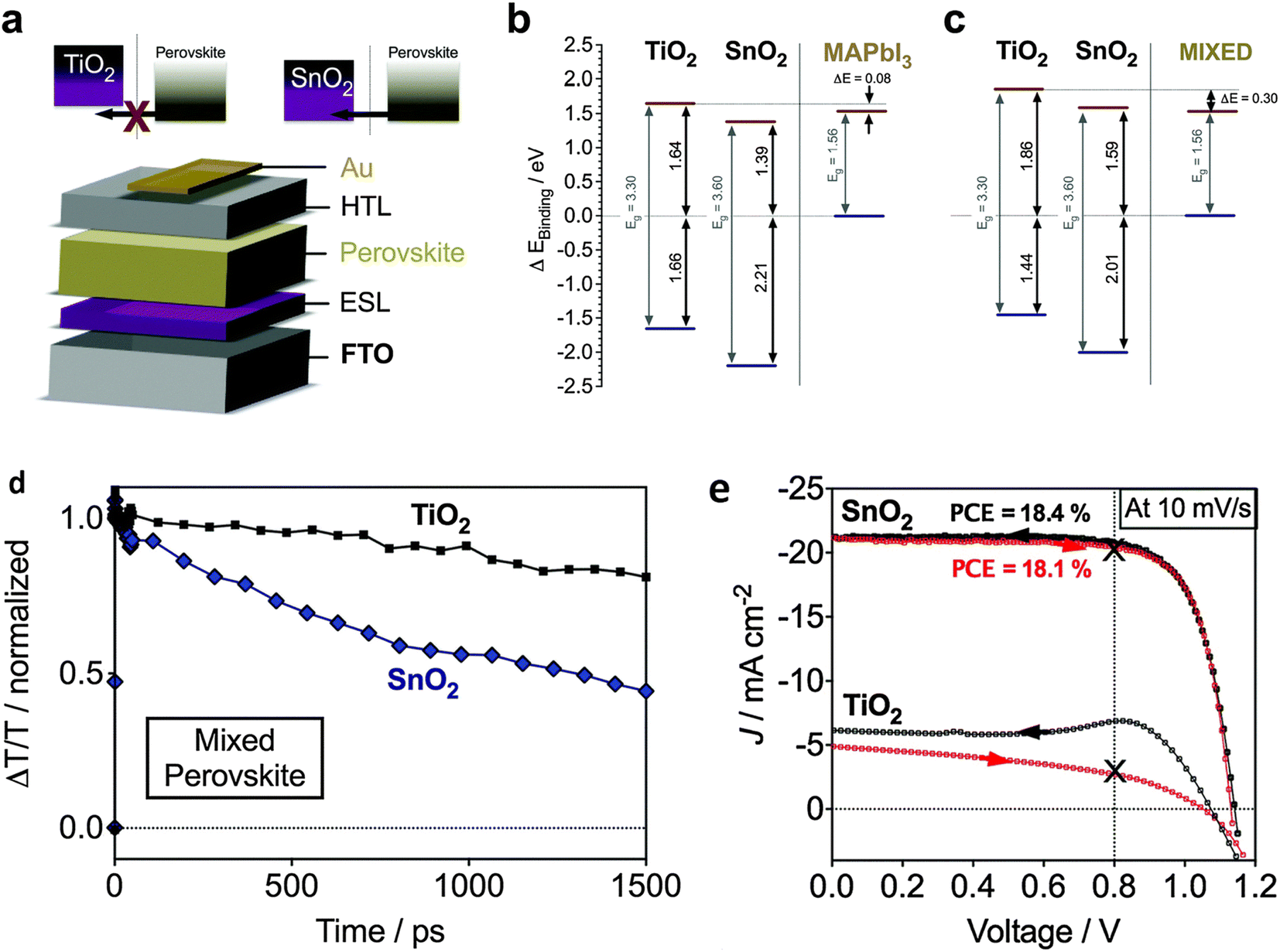 | ||
| Fig. 21 (a–c). Diagram of energy level plans and electron inoculation properties of SnO2- and TiO2-based planar PSCs, (d) transient absorption findings, (e) current–voltage (J–V) curves of TiO2- and SnO2-based planar mixed halide-mixed cation PSCs (reproduced with permission from ref. 184. Copyright 2015 RSC). | ||
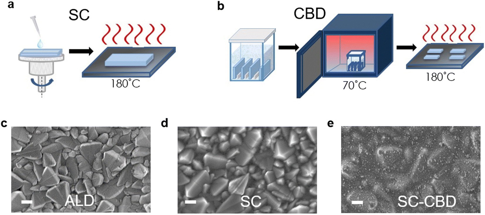 | ||
| Fig. 22 Symbolic diagram showing the preparation of SnO2 thin layers using (a) spin coating (SC) and (b) chemical bath deposition (CBD). (c) Top-view SEM pictures of SnO2 films prepared by atomic layer deposition (ALD), (d) spin coating (SC), and (e) spin coating and chemical bath deposition (SC-CBD). All scale bars are 200 nm (reproduced with permission from ref. 74. Copyright 2016 RSC). | ||
Indium oxide (In2O3) is also an alternative talented ETL that shows outstanding electrical and optical and electrical characteristics, namely better light transmission, fast electron movement, and wide band gap. Employing these benefits, Zhang et al. synthesized a solution-based In2O3 nanocrystalline film ETL for PSCs and attained a PCE above 13%.186 Tungsten oxide (WOx) is alternative, likely, latent n-type material for ETLs that has decent chemical steadiness, a wide band gap, and high electron movement. Chen et al. used WOx as an ESL in PSCs via a facile and solution-processed method, which showed equivalent light transmission and PCE to TiO2, although, they gained an inferior VOC.187
Owing to some outstanding properties such as better chemical and thermal stability and wide band gap, CeOx is also being employed as a talented material for ETLs. However, CeOx has already been utilized in diverse solar cells for its excellent properties, and Wang et al. stated used that CeOx as an ETL material for PSCs.185–190 They established that CeOx-based PSCs could be fabricated using a simplistic sol–gel technique at a low temperature (150 °C). CeOx-based planar PSCs attained PCE of as high as 14.32% with decent stability.191–196
4. High-efficiency PSCs fabrication approaches
4.1. Solution-based methods: one-step versus two-step coatings
In order to fabricate the perovskite absorber layer, usually two approaches are existed, namely, one-stage and two-stage coating approaches. In a one-stage method, a perovskite film was formed via spin-coating a blend of PbI2 and CH3NH3I solution (one-step layer formation) and by spin-coating CH3NH3I later covered with PbI2 (two-stage process). In the case of one-stage layer formation, PbI2 and CH3NH3I CH3NH3I are completely melted using a suitable solvent such as dimethyl sulfoxide (DMSO), N,N-dimethylformamide (DMF), and gamma-butyrolactone (GBL) utilized as a layer formation solution. After spin-coating, drying, and annealing are performed. While, in a two-stage film formation process, a layer of PbI2 was formed by dropping a solution of PbI2 over the substrate surface and after that a solution of CH3NH3I in 2-propanol was webbed over the PbI2 layer (as exhibited in Fig. 23). Two-stage film formation approaches demonstrate better film morphology as compared to one-stage film formation method and resulted in a better cell efficiency,197–199 which specifies that the control of perovskite absorber layer nanostructure is vital in attaining high-performance PSCs.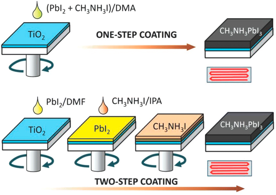 | ||
| Fig. 23 One-stage and two-stage coating methods to prepare CH3NH3PbI3 perovskite layers. DMA, DMF, and IPA signify dimethyl acetamide, dimethyl formamide, and isopropyl alcohol, respectively (reproduced with permission from ref. 197. Copyright 2014 AIP). | ||
In a two-stage film formation approach, the dimensions of CH3NH3PbI3 were pointedly reformed by the concentration of CH3NH3I.200 As the concentration of the CH3NH3I in a 2-propanol solution reduced from 0.063 M to 0.038 M, the typical CH3NH3PbI3 crystal dimensions improved from about 90 nm to about 700 nm, as revealed in Fig. 24.
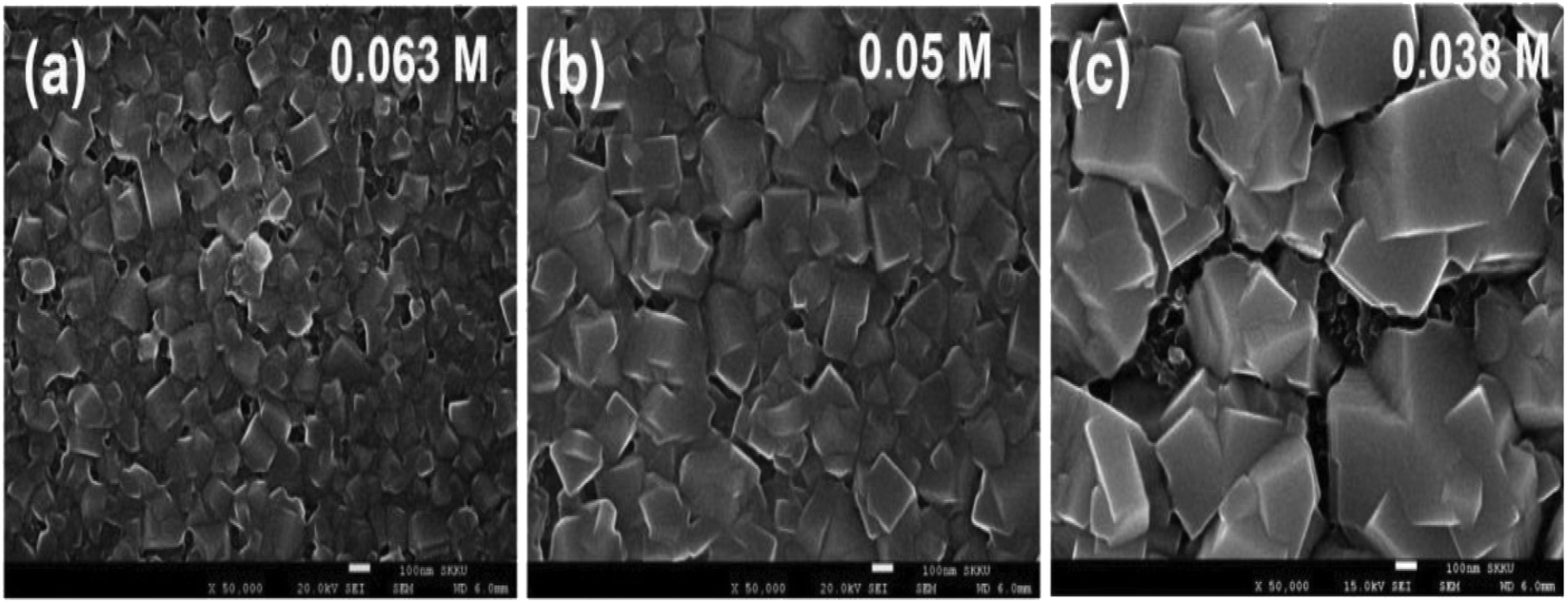 | ||
| Fig. 24 SEM images for CH3NH3PbI3 produced via two-step spin-coating with (a) 0.063 M, (b) 0.05 M, and (c) 0.038 M CH3NH3I solution. Scale bars signify 100 nm (reproduced with permission from ref. 200. Copyright 2014 NPG). | ||
Recently, a two-stage approach was comprehended via a blend of PbI2 and PbCl2. The solubility of PbCl2 can be prominently improved using PbI2 through common ion response. Wand et al. effectively melted PbCl2 salt in DMF by adding PbI2 and then deposited the blend over the mesoporous TiO2 film.201,202 After exposing it to the CH3NH3I mixture, eventually a CH3NH3PbI3−xClx perovskite film with precise morphology was fruitfully attained.203 In Fig. 25, photovoltaic limits are shown as a function of CH3NH3I concentration. For the 0.038 and 0.05 M samples, the average PCE was about 16.3%, while at much concentration of 0.063 M an inferior PCE of 13.4% was gained caused by lower FF and JSC.
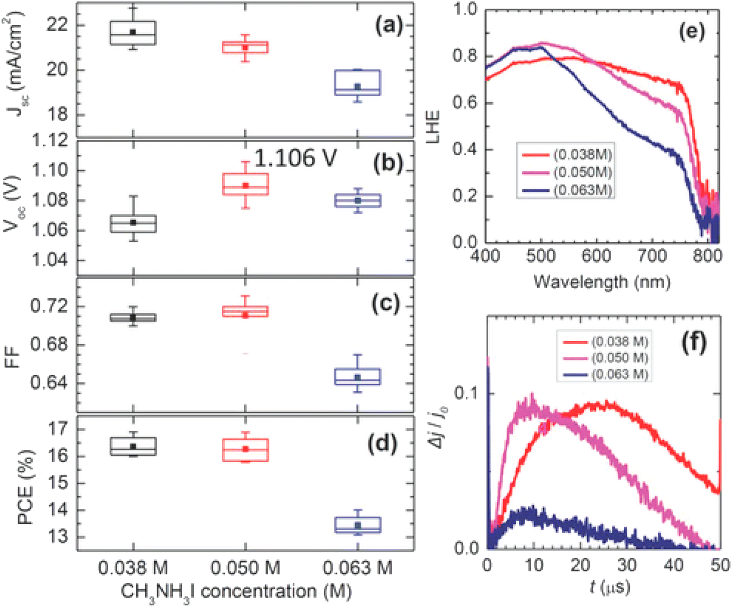 | ||
| Fig. 25 (a–d). JSC, VOC, FF, and PCE, dependent on the CH3NH3I concentration. Error bars in each box denote minimum and maximum values and the middle line in the box signifies the median value. Filled squares in the box denote mean values. (e) Light-capturing efficiency spectra of the CH3NH3PbI3 layers laying on CH3NH3I concentration. (f) Photo-CELIV transients noted for the cells containing FTO/bl-Al2O3/mp-TiO2/MAPbI3/Spiro-MeOTAD/Au, subject to CH3NH3I concentration (reproduced with permission from ref. 200. Copyright 2014 NPG). | ||
It was also observed that bulky crystals formed at lower solution concentrations resulted in superior JSC compared to smaller ones produced using the highly concentrated solution as can be seen in Fig. 25e, and an improved charge-drawing aptitude, as recorded by using photo-CELIV.200,204 It can be clarified in conjunction with the photo-CELIV findings, that an alteration in VOC relates to the rates of charge-drawing and rumination.201,205 In recent years, solvent manufacturing allowed better control over the perovskite film morphology via solution-based methods, unlike vacuum approaches. Liu et al. described that a single-stage film formation approach was superior enough to fabricate even and smooth perovskite layers after it was exposed to chlorobenzene, which brought wild crystallization.206–208 Seok's also introduced an ideal perovskite film formation method via the engineering of a solvent. They utilized a blend of solvents composed of dimethylsulphoxide (DMSO) and γ-butyrolactone trailed by toluene drop-covering, which resulted in the form of smooth perovskite film.202,209,210 The droplet of toluene rapidly detached the extra DMSO solvent present in the wet layer, which directly satisfied the ingredients. To conclude, a regular smooth perovskite film was obtained after heating at 100 °C. Fig. 26 displays an X-ray diffraction (XRD) form of the middle and an SEM figure of the subsequent perovskite film displaying tightly-packed huge grains.
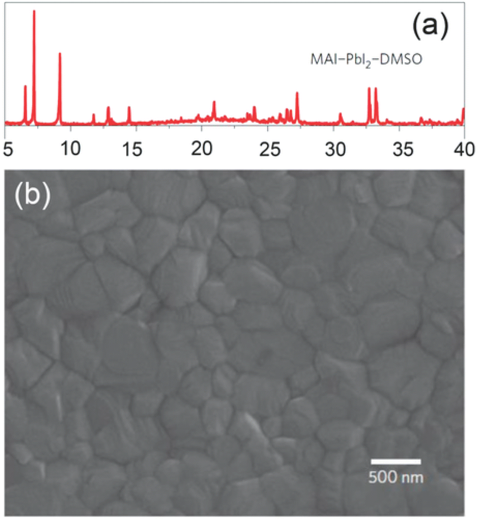 | ||
| Fig. 26 (a) X-ray diffraction shape of an MAI-PbI2-DMSO intermediate stage produced by toluene treatment on the layer deposited by spin-coating of MAI-PbI2-DMSO-GBL solution. (b) SEM image of the subsequent perovskite layer using the middle stage (reproduced with permission from ref. 209 Copyright 2014 NPG). | ||
Additives such as NH4Cl influence the perovskite film was also considered. Ding and Zuo noted an 80.11% FF by adding an NH4Cl additive, which was initiated to improve the morphology and crystallinity of the perovskite film.211
4.2. Perovskite layer formation using the vacuum method
Perovskite layers can also be fabricated via the thermal decomposition of chemicals. Co-evaporation of PbCl2 and CH3NH3I results in a CH3NH3PbI3 stage, and the film smoothness was much improved unlike the solution-based layers,212 as shown in Fig. 27.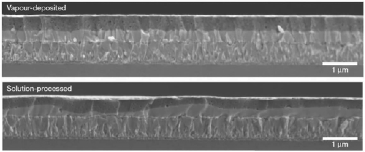 | ||
| Fig. 27 Assessment of the perovskite layer consistency between vapor-deposition and solution-process approaches (reproduced with permission from ref. 212. Copyright 2013 NPG). | ||
A two-source evaporation scheme with ceramic pots was fitted inside the nitrogen-filled glovebox. PbCl2 and CH3NH3I were co-evaporated using distinct containers with a molar ratio of 1![[thin space (1/6-em)]](https://www.rsc.org/images/entities/char_2009.gif) :4. A dusky reddish-brown color was detected, instantly after the evaporation process. The crystallization of perovskite crystals was achieved by annealing.212 Thermal evaporation needs an intense vacuum, which is an expensive way and limited the large-scale fabrication of devices. To overcome this issue, a vapor-supported solution method (VASP), which produces perovskite layers using onsite reactions of deposited layers of PbI2 with CH3NH3I vapor, was established.213 The perovskite layer deposited with the help of this technique presented a better grain assembly with complete surface coverage.
:4. A dusky reddish-brown color was detected, instantly after the evaporation process. The crystallization of perovskite crystals was achieved by annealing.212 Thermal evaporation needs an intense vacuum, which is an expensive way and limited the large-scale fabrication of devices. To overcome this issue, a vapor-supported solution method (VASP), which produces perovskite layers using onsite reactions of deposited layers of PbI2 with CH3NH3I vapor, was established.213 The perovskite layer deposited with the help of this technique presented a better grain assembly with complete surface coverage.
4.3. Manipulation of perovskite absorber morphology
The morphology of perovskite has altered thoroughly since the development of new manufacturing ways and numerous mixed configurations. In this context, the prime task is the creation of high-performance perovskite layers with improved morphology, pinholes-free surface, and better surface coverage. The previous perovskite layers established a dot-like morphology using a one-step spin-coating method that twisted into a three-dimensional nanostructure after using a two-stage sequential deposition method. Furthermore, diverse knowledge has also been established, which is well-suited to the huge-area construction of the perovskite films to avoid the spin-coating method that was mostly utilized for lab-scale cells.4.4. Effect of annealing environment perovskite absorber layer formation
The formation of the perovskite layer using a hot casting of a precursor solution over a heated surface requires extra handling with the heat of the perovskite layer, which is crucial. The circumstances of optimal annealing can also differ by changing the substrate type, layer thickness, and deposition method.214–217 Dualeh et al. established the character of the annealing temperature on the formation of the perovskite layer.215 The consequence of the diverse annealing temperatures was examined in the formation of perovskite films after spin-casting. Scanning electron microscopy (SEM) was used to study the effect of the annealing temperature on the perovskite layer (Fig. 28a–h). An extreme modification was detected in the morphology of the perovskite film at 80 °C (annealing temperature). When the annealing temperature was 100 °C, the perovskite layer was reasonably similar to that molded at 80 °C (Fig. 28b and c), in spite of the duration needed for the conversion was longer at 80 °C. Additionally, after the annealing temperature reached 120 °C, the perovskite layer assumed a bigger separate size (Fig. 28d). It was detected that with the enrichment in the annealing temperature, perovskite crystals converted to a larger shape (Fig. 28e–g). Henceforth, Fig. 28a–g obviously proved that perovskite formation is meaningfully inclined towards annealing temperature. W. Nie et al. described a solution-processed hot-casting method to attain ∼18% PCE with one millimeter-scale crystal grains.218 It was noticed that grain size presented an exclusive leaf-like design glowing from the center of the grain (Fig. 28i). Though, Y. Deng et al. clarified a comparable type of design using Rayleigh–Benard convection, which springs a promising approach on millimeter-scale crystalline grains.219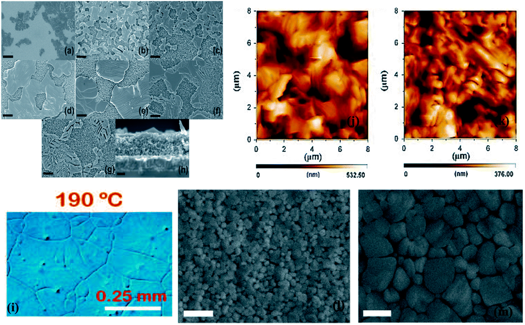 | ||
| Fig. 28 Scanning electron microscope pictures of m-TiO2 layers with the prepared perovskite solution heat-treated at various temperatures (a) 60 °C, (b) 80 °C, (c) 100 °C, (d) 120 °C, (e) 150 °C, (f) 175 °C, and (g) 200 °C. (h) Side view SEM image of the sample annealed at 150 °C. Black scale bars parallel to (a) 5 μm, (b–g) 1 μm, and (h) 200 nm102 Optical micrographs of the CH3NH3PbI3−xClx perovskite layer (i).215 AFM pictures of perovskite layer toughened with the one-step technique (j), multi-step way (k) (reproduced with permission from ref. 218. Copyright 2015 AAAS). Scanning electron microscope picture of an unannealed hot-cast layer (l) and an annealed hot-cast layer (m), displaying that the perovskite crystals produce while annealing (reproduced with permission from 217 Copyright 2015 Elsevier). | ||
Muscarella et al. also established a novel, air-stable method for CH3NH3PbI3 perovskites.220 In Fig. 28l and m SEM micrographs of unannealed and annealed hot-deposited materials, respectively, are revealed, which discloses that the size of perovskite crystals rises throughout the post-formation annealing. Wu et al. stated the low-pressure supported method together with thermal heating in the film formation of double perovskite Cs2AgBiBr6.221 Because of low-pressure dealing before annealing, double perovskite film presented dense and smooth morphology, unlike that in the conservative thermal annealing technique.
4.5. Formation of perovskite absorber layer as a function of precursor aging
It was detected that the aging of precursor has an prominent consequence on the formation of thin film, the density of the trap state, and uniformity.222 P. Boonmongkolras et al. established the connection between the perovskite precursor solution aging period and the triple cation perovskite Cs0.05(FA0.83MA0.17)0.95Pb(I0.83Br0.17)3 cell efficiency.223 It was detected that cells that are made up using 6 hours old solution display the supreme average efficiency with the finest delivery and improved duplicability (Fig. 29a).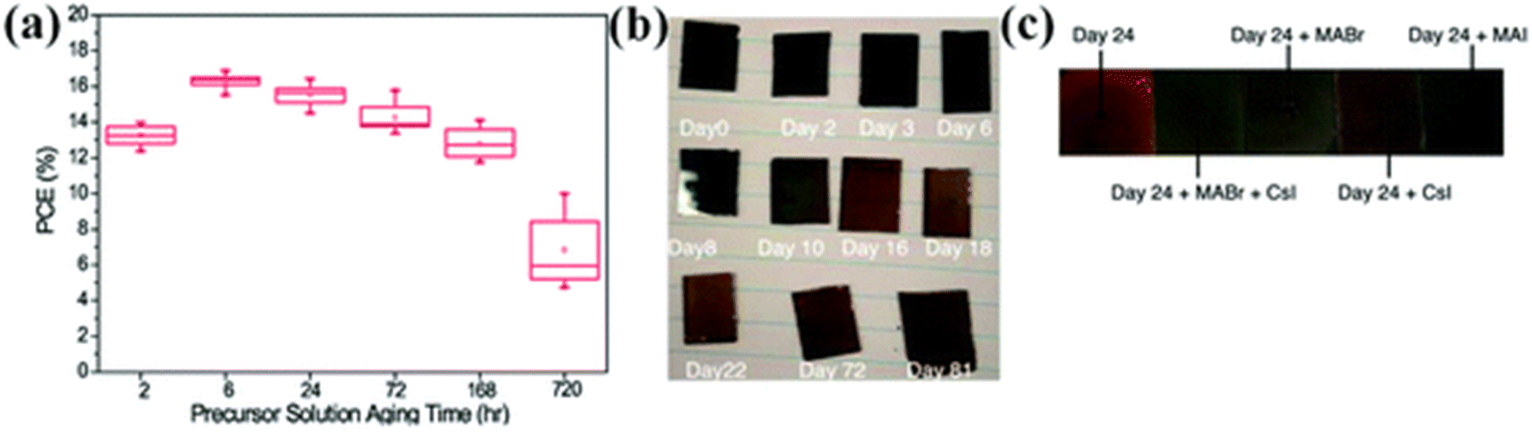 | ||
| Fig. 29 (a) PCE distribution with precursor solution aging time (hours) of the triple-cation lead halide PSCs.223 (b) Photographs of triple-cation (FA, MA, Cs) films produced from fresh ink (viz., 0 days of storage, labeled as “Day 0”) and the same ink is utilized for the 2–81 days storage. (c) Snapshots of layers made up from 24 days old ink. (Reproduced with permission from ref. 224. Copyright 2020 ACS). | ||
The deprivation structure in triple cation perovskite films was clarified by B. Dou et al.224 The snaps of perovskite layers with loading days are revealed in Fig. 29b and the photographs of perovskite layers made-up from 24 days aged ink are exposed in Fig. 29c. It was detected that the perovskite film grows lighter with bigger storage days. The perovskite layer roughness and thickness were also influenced by solution aging.
4.6. Formation of perovskite absorber layer as a function of precursor temperature
PSCs are typically fabricated using preheated perovskite mixtures. G. Namkoong et al. discover the fundamental reason for the effect of temperature on PSCs. Perovskite (MAPbI3−xClx) solution was cast-off after heating using numerous temperatures of 40 °C, 70 °C, and 90 °C for 24 h, and thin layers were spin-coated in a nitrogen gas-filled glove box.225Fig. 30 displays the formation of CH3NH3PbI3−xClx layers spin-casted over preheated glass substrate at 180 °C with dissimilar temperatures. The normal grain size at 70 °C is far greater compared to the solution heated at 40 °C, nevertheless, at 90 °C, there is a fall in grain size. The layer thickness was also affected by the solution temperature. Thickness was found as 210 ± 8 nm, 252 ± 7 nm, and 270 ± 6 nm using different solution temperatures of 40 °C, 70 °C, and 90 °C, respectively.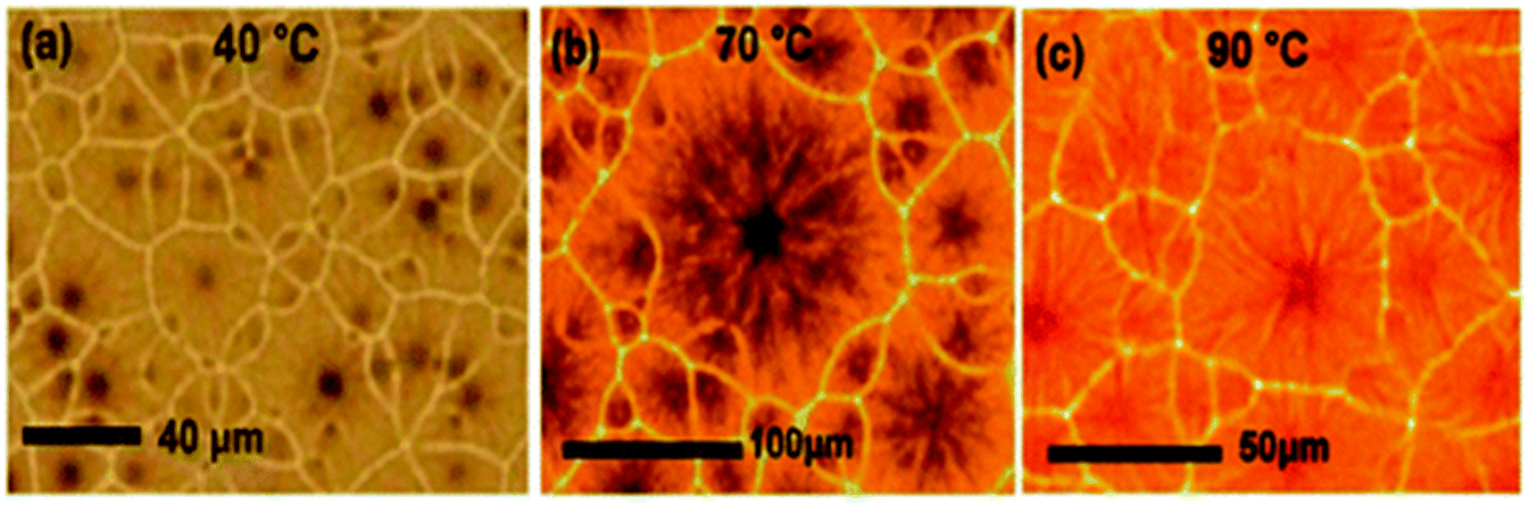 | ||
| Fig. 30 Optical microscopic images of the perovskite thin layer by varying perovskite solution temperatures of (a) 40 °C, (b) 70 °C, and (c) 90 °C (reproduced with permission from ref. 225. Copyright 2018 Elsevier). | ||
4.7. Effect of post-device ligand (PDL) treatment on the morphology of the perovskite absorber layer
H. Zhang et al. offered the elementary post-device ligand (PDL) behavior to meaningfully improve the stability and performance of PSCs.225 In the report, diethylenetriamine (DETA) with three amine groups was used as a ligand to modify PSCs. In Fig. 31a and b top view SEM image is revealed and no big alteration in the grain size was detected after PDL treatment. The histograms of the cell efficiencies are shown in Fig. 31c.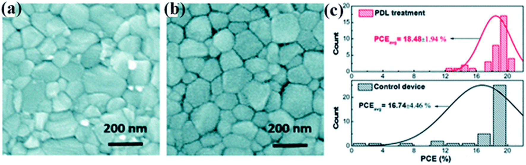 | ||
| Fig. 31 SEM top view pictures of perovskite thin layers (a) without any treatment and (b) with post-device ligand treatment. (c) Histograms of the device efficiencies with PDL treatment and without any treatment (37 cells were made-up and verified, reproduced with permission from ref. 225. Copyright 2018 Elsevier). | ||
The PDL treatment significantly improves the device duplicability with a standard deviation of just 1.94%. In the short-term, the steadiness of the treated cells without any illustration astonishingly improves, with 70% efficiency reserved at ambient environments after a 500 hours maximum-power-point trailing trial, while the control device will totally break down within 100 hours.225
5. Role of interface engineering in perovskite devices
The development of interfaces in PSCs has been a real means to improve stability and photovoltaic performance. M. M. Tavakoli et al. established a perovskite device adopting an improved ETL with a PCE of 20.94% (Fig. 32a and b). A single layer of graphene was inserted at the boundary of ZnO ETL and perovskite light absorber. Amazingly, the author found that the insertion of a graphene monolayer at the ETL/perovskite border improves the carrier withdrawal and photovoltaic characteristics. Cell stability was further improved by passivating the perovskite layer using another modulator, i.e., 3-(pentafluorophenyl)-propionamide (PFPA) to decrease the superficial trap states of the perovskite.235 The stability findings display that the passivated device on MLG/ZnO retained 93% of its early PCE rate even after 300 h under constant radiance (Fig. 32c). X. X. Gao et al. proved that by means of the conjugated polymers (PD-10-DTTE-7) with both the acceptor and donor alkylated as an interlayer between MAPbI3 and doped Spiro-OMeTAD can meaningfully improve the efficiency of solar cells.235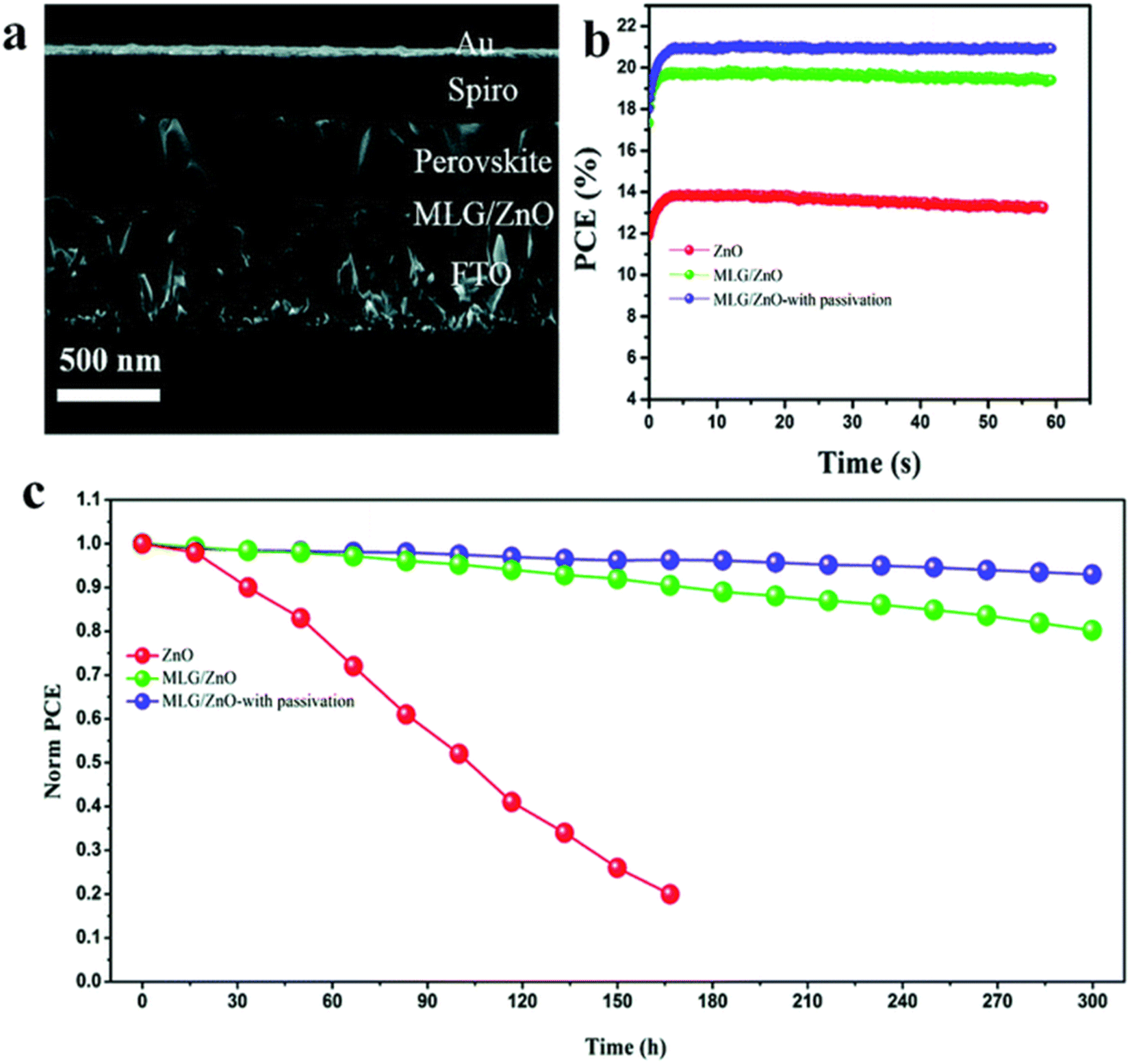 | ||
| Fig. 32 (a) Side view SEM image of the PSC fabricated using MLG/ZnO. (b) PCE curve with time under maximum power point tracking. (c) Stability test of PSCs based on ZnO, MLG/ZnO, and MLG/ZnO with passivation under constant illumination for 300 hours at room temperature and under nitrogen flow (reproduced with permission from ref. 235. Copyright 2019 RSC). | ||
Atomic-force microscopy (AFM) examination discloses that the roughness value was 24.6 nm for the MAPbI3 layer and 16.3 nm for the PD-10-DTTE-7/MAPbI3 film. Using the custom-made boundary, the MAPbI3 devices with the PD-10-DTTE-7 interlayer displayed the best PCE of 18.83%. The surface nanostructure of dissimilar films was examined using a top-view SEM using various magnifications. Fig. 33a–c displays that tetracene and perovskite films are dense polycrystalline with micrometer grain size while Spiro accepts a conformal layer Fig. 33d, confirming total surface treatment of the mutual HTLs.236 J. Lu et al. introduced a simple method to expand the PCE and elevated the PSCs stability by modifying the interface between the HTL and light-harvester. Using replicated solar cell working environments (1 sun AM1.5G irradiation, 50% RH, 50 °C device temperature), such cells engaged more than 80% of their early photovoltaic performance after 50 h and worked stably for the next 135 h.236
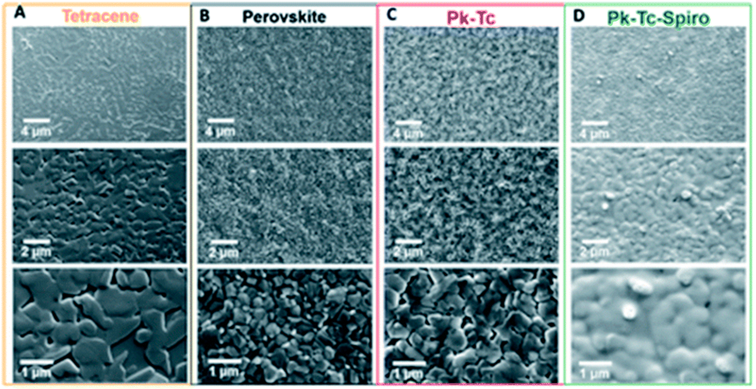 | ||
| Fig. 33 Top-view scanning electron microscopy of (A) tetracene (Tc) single coat, (B) perovskite (Pk), (C) perovskite–tetracene (Pk–Tc), and (D) perovskite–tetracene–Spiro (Pk–Tc–Spiro) layers at three diverse magnifications (reproduced with permission from ref. 236. Copyright 2019 AAAS). | ||
A two-sided border alteration to perovskites by doping with CsPbBr3 nanocrystals (CN) was also described. It was found that CN efficiently overcomes the flaw at the SnO2/perovskite border and improves the interfacial electron transfer.237 Furthermore, by introducing the hybrid density functional theory (DFT) based simulations, an interface was created between the fluorinated Zn-phthalocyanine (FnZnPc) and MAPbI3 surface. It was observed that FnZnPc procedures a steady boundary with the MAPbI3 surface with obligatory energies compared to the unsubstituted case.238
6. Conclusions
Since the progress of solid-state perovskite solar cells in 2012, the efficiency of these devices has offered an extraordinarily swift improvement from 9.7% to 25.2% in less than 10 years. Initiated by the advancement of the perovskite solar cell in 2012, profound development in structure scheme, materials understanding, method engineering, and device physics has paid to the innovatory advancement of the perovskite solar cell to be a robust contestant for a next-generation solar energy mower. The superior efficiency together with the inexpensive materials and procedures are the trade points of these devices over profit-making silicon or other inorganic and organic solar cells. Since an extraordinary performance is directly connected to the device arrangement, understanding the device dynamics and device construction engineering is of dire significance, although, the interfaces and materials used in the perovskite devices are similarly vital for attaining maximum device performance. On the other hand, an optimum fabrication procedure must be established, precisely for excellent perovskite films, since the perovskite light absorber is the crucial component in the perovskite devices. Moreover, the growth of low-bandgap perovskite materials built on a Sn/Pb diverse composition has made it conceivable to construct perovskite/perovskite tandem solar cells. Modifying the bandgap of these materials, while reducing the possible damage, will ease extra improvements in the efficiency to >30%. Investigations on perovskite devices are continuing, and it is predictable that they will show an important part in the upcoming solar energy. It is vital to (1) produce effective and stable perovskite materials, (2) participate in emerging suitable tools and procedures for making mini-modules, (3) launch close partnerships between companies and academia to report the persistent matters in emerging large-sized cells, and (4) introduce vigorous testing measures to precisely measure the long-term steadiness of perovskites.Conflicts of interest
There are no conflicts to declare.Acknowledgements
The authors gratefully acknowledge the financial support from the Higher Education Commission (HEC) of Pakistan.References
- Q. Wang, et al., Progress in emerging solution-processed thin film solar cells–Part I: Polymer solar cells, Renewable Sustainable Energy Rev., 2016, 56, 347–361 CrossRef CAS.
- J. Jaksik, et al., Nanostructured functional materials for advanced three-dimensional (3D) solar cells, Sol. Energy Mater. Sol. Cells, 2017, 167, 121–132 CrossRef CAS.
- J. Mohtasham, Renewable energies, Energy Procedia, 2015, 74, 1289–1297 CrossRef.
- O. Ellabban, H. Abu-Rub and F. Blaabjerg, Renewable energy resources: Current status, future prospects and their enabling technology, Renewable Sustainable Energy Rev., 2014, 39, 748–764 CrossRef.
- N. S. Lewis, Toward cost-effective solar energy use, science, 2007, 315(5813), 798–801 CrossRef CAS PubMed.
- M. Green, et al., Solar cell efficiency tables (version 57), Prog. Photovolt.: Res. Appl., 2021, 29(1), 3–15 CrossRef.
- J. Euvrard, Y. Yan and D. B. Mitzi, Electrical doping in halide perovskites, Nat. Rev. Mater., 2021, 6(6), 531–549 CrossRef CAS.
- D. Weber, CH3NH3PbX3, ein Pb (II)-system mit kubischer perowskitstruktur/CH3NH3PbX3, a Pb (II)-system with cubic perovskite structure, Z. Naturforsch. B, 1978, 33(12), 1443–1445 CrossRef.
- D. Weber, CH3NH3SnBrxI3−x (x = 0–3), ein Sn (II)-System mit kubischer Perowskitstruktur/CH3NH3SnBrxI3−x (x= 0–3), a Sn (II)-system with cubic perovskite structure, Z. Naturforsch. B, 1978, 33(8), 862–865 CrossRef.
- L. Li and M. Yan, Recent progress in the development of RE2TMTM′O6 double perovskite oxides for cryogenic magnetic refrigeration, J. Mater. Sci. Technol., 2023, 136, 1–12 CrossRef.
- D. Mitzi, et al., Conducting layered organic-inorganic halides containing 〈110〉-oriented perovskite sheets, Science, 1995, 267(5203), 1473–1476 CrossRef CAS PubMed.
- A. Kojima, et al., Organometal halide perovskites as visible-light sensitizers for photovoltaic cells, J. Am. Chem. Soc., 2009, 131(17), 6050–6051 CrossRef CAS PubMed.
- G. Yu, et al., Polymer photovoltaic cells: enhanced efficiencies via a network of internal donor–acceptor heterojunctions, Science, 1995, 270(5243), 1789–1791 CrossRef CAS.
- J. Xu, et al., Efficiently photo-charging lithium-ion battery by perovskite solar cell, Nat. Commun., 2015, 6(1), 1–7 Search PubMed.
- Q. Dong, et al., Electron-hole diffusion lengths >175 μm in solution-grown CH3NH3PbI3 single crystals, Science, 2015, 347(6225), 967–970 CrossRef CAS PubMed.
- L. P. Lekesi, et al., Developments on Perovskite Solar Cells (PSCs): A Critical Review, Appl. Sci., 2022, 12(2), 672 CrossRef CAS.
- V. D'innocenzo, et al., Excitons versus free charges in organo-lead tri-halide perovskites, Nat. Commun., 2014, 5(1), 1–6 Search PubMed.
- M. Saba, et al., Excited state properties of hybrid perovskites, Acc. Chem. Res., 2016, 49(1), 166–173 CrossRef CAS PubMed.
- F. Giustino and H. J. Snaith, Toward lead-free perovskite solar cells, ACS Energy Lett., 2016, 1(6), 1233–1240 CrossRef CAS.
- L. De Marco, et al., Perovskite Single-Crystal Solar Cells: Advances and Challenges, Sol. RRL, 2022, 6(7), 2101085 CrossRef CAS.
- T. A. Berhe, et al., Organometal halide perovskite solar cells: degradation and stability, Energy Environ. Sci., 2016, 9(2), 323–356 RSC.
- S. Yang, et al., Recent advances in perovskite solar cells: efficiency, stability and lead-free perovskite, J. Mater. Chem. A, 2017, 5(23), 11462–11482 RSC.
- Z. Chchiyai, et al., Effect of cobalt doping on the crystal structure, magnetic, dielectric, electrical and optical properties of PbTi1−xCoxO3−δ perovskite materials, J. Alloys Compd., 2022, 927, 166979 CrossRef CAS.
- M. Habibi, et al., Progress in emerging solution-processed thin film solar cells–Part II: Perovskite solar cells, Renewable Sustainable Energy Rev., 2016, 62, 1012–1031 CrossRef CAS.
- N.-G. Park, Perovskite solar cells: an emerging photovoltaic technology, Mater. Today, 2015, 18(2), 65–72 CrossRef CAS.
- C. Li, et al., Formability of abx3 (x= f, cl, br, i) halide perovskites, Acta Crystallogr., Sect. B: Struct. Sci., 2008, 64(6), 702–707 CrossRef CAS PubMed.
- V. M. Goldschmidt, Die gesetze der krystallochemie, Naturwissenschaften, 1926, 14(21), 477–485 CrossRef CAS.
- M. A. Green, A. Ho-Baillie and H. J. Snaith, The emergence of perovskite solar cells, Nat. Photonics, 2014, 8(7), 506–514 CrossRef CAS.
- M. Asghar, et al., Device stability of perovskite solar cells–A review, Renewable Sustainable Energy Rev., 2017, 77, 131–146 CrossRef CAS.
- J. Chen and N.-G. Park, Inorganic hole transporting materials for stable and high efficiency perovskite solar cells, J. Phys. Chem. C, 2018, 122(25), 14039–14063 CrossRef CAS.
- H. Fujiwara, Hybrid Perovskite Solar Cells: Characteristics and Operation, John Wiley & Sons, 2022 Search PubMed.
- N. Marinova, S. Valero and J. L. Delgado, Organic and perovskite solar cells: Working principles, materials and interfaces, J. Colloid Interface Sci., 2017, 488, 373–389 CrossRef CAS PubMed.
- H.-S. Kim, et al., Lead iodide perovskite sensitized all-solid-state submicron thin film mesoscopic solar cell with efficiency exceeding 9%, Sci. Rep., 2012, 2(1), 1–7 CrossRef PubMed.
- H. Zhou, et al., Interface engineering of highly efficient perovskite solar cells, Science, 2014, 345(6196), 542–546 CrossRef CAS PubMed.
- Z. Song, et al., Perovskite solar cells go bifacial—mutual benefits for efficiency and durability, Adv. Mater., 2022, 34(4), 2106805 CrossRef CAS PubMed.
- Z. Song, et al., Pathways toward high-performance perovskite solar cells: review of recent advances in organo-metal halide perovskites for photovoltaic applications, J. Photonics Energy, 2016, 6(2), 022001 CrossRef.
- J. Wei, et al., Hysteresis analysis based on the ferroelectric effect in hybrid perovskite solar cells, J. Phys. Chem. Lett., 2014, 5(21), 3937–3945 CrossRef CAS PubMed.
- H.-S. Kim, et al., Control of I–V hysteresis in CH3NH3PbI3 perovskite solar cell, J. Phys. Chem. Lett., 2015, 6(22), 4633–4639 CrossRef CAS PubMed.
- B. Chen, et al., Origin of J–V hysteresis in perovskite solar cells, J. Phys. Chem. Lett., 2016, 7(5), 905–917 CrossRef CAS PubMed.
- Z. Shi and A. H. Jayatissa, Perovskites-based solar cells: A review of recent progress, materials and processing methods, Materials, 2018, 11(5), 729 CrossRef PubMed.
- L. Yin, et al., Functionalized-MXene-nanosheet-doped tin oxide enhances the electrical properties in perovskite solar cells, Cell Rep. Phys. Sci., 2022, 3(6), 100905 CrossRef CAS.
- L. Meng, et al., Recent advances in the inverted planar structure of perovskite solar cells, Acc. Chem. Res., 2016, 49(1), 155–165 CrossRef CAS PubMed.
- J. Y. Jeng, et al., CH3NH3PbI3 perovskite/fullerene planar-heterojunction hybrid solar cells, Adv. Mater., 2013, 25(27), 3727–3732 CrossRef CAS PubMed.
- L. Etgar, et al., Mesoscopic CH3NH3PbI3/TiO2 heterojunction solar cells, J. Am. Chem. Soc., 2012, 134(42), 17396–17399 CrossRef CAS PubMed.
- Y. Yang, et al., Perovskite Solar Cells Based Self-Charging Power Packs Fundamentals, Applications and Challenges, Nano Energy, 2022, 106910 CrossRef CAS.
- L. Huang, et al., Toward revealing the critical role of perovskite coverage in highly efficient electron-transport layer-free perovskite solar cells: an energy band and equivalent circuit model perspective, ACS Appl. Mater. Interfaces, 2016, 8(15), 9811–9820 CrossRef CAS PubMed.
- Q. Hu, et al., Engineering of electron-selective contact for perovskite solar cells with efficiency exceeding 15, ACS Nano, 2014, 8(10), 10161–10167 CrossRef CAS PubMed.
- W. Ke, et al., Efficient hole-blocking layer-free planar halide perovskite thin-film solar cells, Nat. Commun., 2015, 6(1), 1–7 Search PubMed.
- D. Prochowicz, et al., Mechanosynthesis of pure phase mixed-cation MAxFA1−x PbI3 hybrid perovskites: photovoltaic performance and electrochemical properties, Sustainable Energy Fuels, 2017, 1(4), 689–693 RSC.
- W. S. Yang, et al., High-performance photovoltaic perovskite layers fabricated through intramolecular exchange, Science, 2015, 348(6240), 1234–1237 CrossRef CAS PubMed.
- D. M. Jang, et al., Reversible halide exchange reaction of organometal trihalide perovskite colloidal nanocrystals for full-range band gap tuning, Nano Lett., 2015, 15(8), 5191–5199 CrossRef CAS PubMed.
- W.-J. Yin, et al., Halide perovskite materials for solar cells: a theoretical review, J. Mater. Chem. A, 2015, 3(17), 8926–8942 RSC.
- L. Huang, et al., Efficient planar perovskite solar cells without a high temperature processed titanium dioxide electron transport layer, Sol. Energy Mater. Sol. Cells, 2016, 149, 1–8 CrossRef CAS.
- J. W. Lee, et al., High-efficiency perovskite solar cells based on the black polymorph of HC(NH2)2PbI3, Adv. Mater., 2014, 26(29), 4991–4998 CrossRef CAS PubMed.
- Q. Zhu, et al., Compact layer free perovskite solar cells with a high-mobility hole-transporting layer, ACS Appl. Mater. Interfaces, 2016, 8(4), 2652–2657 CrossRef CAS PubMed.
- S. Aharon, et al., Depletion region effect of highly efficient hole conductor free CH3 NH3 PbI3 perovskite solar cells, Phys. Chem. Chem. Phys., 2014, 16(22), 10512–10518 RSC.
- F. C. Hanusch, et al., Efficient planar heterojunction perovskite solar cells based on formamidinium lead bromide, J. Phys. Chem. Lett., 2014, 5, 2791–2795 CrossRef CAS PubMed.
- N. J. Jeon, et al., Compositional engineering of perovskite materials for high-performance solar cells, Nature, 2015, 517(7535), 476–480 CrossRef CAS PubMed.
- N. Pellet, et al., Mixed-organic-cation Perovskite photovoltaics for enhanced solar-light harvesting, Angew. Chem., 2014, 126(12), 3215–3221 CrossRef.
- J.-P. Correa-Baena, et al., The rapid evolution of highly efficient perovskite solar cells, Energy Environ. Sci., 2017, 10(3), 710–727 RSC.
- M. Saliba, et al., Incorporation of rubidium cations into perovskite solar cells improves photovoltaic performance, Science, 2016, 354(6309), 206–209 CrossRef CAS PubMed.
- M. Saliba, et al., Cesium-containing triple cation perovskite solar cells: improved stability, reproducibility and high efficiency, Energy Environ. Sci., 2016, 9(6), 1989–1997 RSC.
- H. Choi, et al., Cesium-doped methylammonium lead iodide perovskite light absorber for hybrid solar cells, Nano Energy, 2014, 7, 80–85 CrossRef CAS.
- Y. Liu, et al., Two-inch-sized perovskite CH3NH3PbX3 (X = Cl, Br, I) crystals: growth and characterization, Adv. Mater., 2015, 27(35), 5176–5183 CrossRef CAS PubMed.
- B. Suarez, et al., Recombination study of combined halides (Cl, Br, I) perovskite solar cells, J. Phys. Chem. Lett., 2014, 5(10), 1628–1635 CrossRef CAS PubMed.
- E. Edri, et al., Chloride inclusion and hole transport material doping to improve methyl ammonium lead bromide perovskite-based high open-circuit voltage solar cells, J. Phys. Chem. Lett., 2014, 5(3), 429–433 CrossRef CAS PubMed.
- S. Seo, et al., An ultra-thin, un-doped NiO hole transporting layer of highly efficient (16.4%) organic–inorganic hybrid perovskite solar cells, Nanoscale, 2016, 8(22), 11403–11412 RSC.
- M. M. Lee, et al., Efficient hybrid solar cells based on meso-superstructured organometal halide perovskites, Science, 2012, 338(6107), 643–647 CrossRef CAS PubMed.
- J. H. Noh, et al., Chemical management for colorful, efficient, and stable inorganic–organic hybrid nanostructured solar cells, Nano Lett., 2013, 13(4), 1764–1769 CrossRef CAS PubMed.
- H. Choi, et al., Cesium-doped methylammonium lead iodide perovskite light absorber for hybrid solar cells, Nano Energy, 2014, 7, 80–85 CrossRef CAS.
- T. J. Jacobsson, et al., Exploration of the compositional space for mixed lead halogen perovskites for high efficiency solar cells, Energy Environ. Sci., 2016, 9(5), 1706–1724 RSC.
- N. K. Noel, et al., Lead-free organic–inorganic tin halide perovskites for photovoltaic applications, Energy Environ. Sci., 2014, 7(9), 3061–3068 RSC.
- W.-J. Yin, Y. Yan and S.-H. Wei, Anomalous alloy properties in mixed halide perovskites, J. Phys. Chem. Lett., 2014, 5(21), 3625–3631 CrossRef CAS PubMed.
- E. H. Anaraki, et al., Highly efficient and stable planar perovskite solar cells by solution-processed tin oxide, Energy Environ. Sci., 2016, 9(10), 3128–3134 RSC.
- A. Sharma, A comprehensive study of solar power in India and World, Renewable Sustainable Energy Rev., 2011, 15(4), 1767–1776 CrossRef.
- N. Kannan and D. Vakeesan, Solar energy for future world:-A review, Renewable Sustainable Energy Rev., 2016, 62, 1092–1105 CrossRef.
- B. W. Park, et al., Bismuth based hybrid perovskites A3Bi2I9 (A: methylammonium or cesium) for solar cell application, Adv. 2D Mater., 2015, 27(43), 6806–6813 CrossRef CAS PubMed.
- S. Sen, et al., Renewable energy scenario in India: Opportunities and challenges, J. Afr. Earth Sci., 2016, 122, 25–31 CrossRef.
- A. Kumar, et al., Renewable energy in India: current status and future potentials, Renewable Sustainable Energy Rev., 2010, 14(8), 2434–2442 CrossRef.
- H. Tang, S. He and C. Peng, A short progress report on high-efficiency perovskite solar cells, Nanoscale Res. Lett., 2017, 12(1), 1–8 CrossRef CAS PubMed.
- K. Kaygusuz, Energy for sustainable development: key issues and challenges, Energy Sources, Part B, 2007, 2(1), 73–83 CrossRef CAS.
- Z. Wang, et al., Stability of perovskite solar cells: a prospective on the substitution of the A cation and X anion, Angew. Chem., Int. Ed., 2017, 56(5), 1190–1212 CrossRef CAS PubMed.
- J. Gong, C. Li and M. R. Wasielewski, Advances in solar energy conversion, Chem. Soc. Rev., 2019, 48(7), 1862–1864 RSC.
- M. B. Hayat, et al., Solar energy—A look into power generation, challenges, and a solar-powered future, Int. J. Energy Res., 2019, 43(3), 1049–1067 CrossRef.
- E. Kabir, et al., Solar energy: Potential and future prospects, Renewable Sustainable Energy Rev., 2018, 82, 894–900 CrossRef.
- H. J. Snaith, Perovskites: the emergence of a new era for low-cost, high-efficiency solar cells, J. Phys. Chem. Lett., 2013, 4(21), 3623–3630 CrossRef CAS.
- R. Wang, et al., A review of perovskites solar cell stability, Adv. Funct. Mater., 2019, 29(47), 1808843 CrossRef CAS.
- S. K. Hau, H.-L. Yip and A. K.-Y. Jen, A review on the development of the inverted polymer solar cell architecture, Polym. Rev., 2010, 50(4), 474–510 CrossRef CAS.
- A. M. Humada, et al., Solar cell parameters extraction based on single and double-diode models: A review, Renewable Sustainable Energy Rev., 2016, 56, 494–509 CrossRef.
- P. K. Nayak, et al., Photovoltaic solar cell technologies: analysing the state of the art, Nat. Rev. Mater., 2019, 4(4), 269–285 CrossRef CAS.
- A. Kumar, et al., Efficient and stable perovskite solar cells by interface engineering at the interface of electron transport layer/perovskite, Opt. Mater., 2022, 132, 112846 CrossRef CAS.
- J. Gong, et al., Review on dye-sensitized solar cells (DSSCs): Advanced techniques and research trends, Renewable Sustainable Energy Rev., 2017, 68, 234–246 CrossRef CAS.
- N. A. Ludin, et al., Review on the development of natural dye photosensitizer for dye-sensitized solar cells, Renewable Sustainable Energy Rev., 2014, 31, 386–396 CrossRef CAS.
- Z. Hu, et al., A critical review on semitransparent organic solar cells, Nano Energy, 2020, 78, 105376 CrossRef CAS.
- J. Yan and B. R. Saunders, Third-generation solar cells: a review and comparison of polymer: fullerene, hybrid polymer and perovskite solar cells, RSC Adv., 2014, 4(82), 43286–43314 RSC.
- P. Zhao, B. J. Kim and H. S. Jung, Passivation in perovskite solar cells: A review, Mater. Today Energy, 2018, 7, 267–286 CrossRef.
- A. Raj, et al., Evidence of improved power conversion efficiency in lead-free CsGeI3 based perovskite solar cell heterostructure via scaps simulation, J. Vac. Sci. Technol. B:Nanotechnol. Microelectron., 2021, 39(1), 012401 CrossRef CAS.
- M. Kumar, et al., Theoretical evidence of high power conversion efficiency in double perovskite solar cell device, Opt. Mater., 2021, 111, 110565 CrossRef CAS.
- L. Chu, Pseudohalide anion engineering for highly efficient and stable perovskite solar cells, Matter, 2021, 4(6), 1762–1764 CrossRef CAS.
- S. Bai, et al., Planar perovskite solar cells with long-term stability using ionic liquid additives, Nature, 2019, 571(7764), 245–250 CrossRef CAS PubMed.
- V. Zardetto, et al., Atomic layer deposition for perovskite solar cells: research status, opportunities and challenges, Sustainable Energy Fuels, 2017, 1(1), 30–55 RSC.
- M. I. H. Ansari, A. Qurashi and M. K. Nazeeruddin, Frontiers, opportunities, and challenges in perovskite solar cells: A critical review, J. Photochem. Photobiol., 2018, 35, 1–24 CrossRef CAS.
- S. Ravishankar, et al., Influence of Charge Transport Layers on Open-Circuit Voltage and Hysteresis in Perovskite Solar Cells, Joule, 2018, 2(4), 788–798 CrossRef CAS.
- A. K. Al-Mousoi, et al., Simulation and analysis of lead-free perovskite solar cells incorporating cerium oxide as electron transporting layer, RSC Adv., 2022, 12(50), 32365–32373 RSC.
- P. Docampo, et al., Efficient organometal trihalide perovskite planar-heterojunction solar cells on flexible polymer substrates, Nat. Commun., 2013, 4(1), 1–6 CrossRef PubMed.
- Y.-F. Chiang, et al., High voltage and efficient bilayer heterojunction solar cells based on an organic–inorganic hybrid perovskite absorber with a low-cost flexible substrate, Phys. Chem. Chem. Phys., 2014, 16(13), 6033–6040 RSC.
- N. Akhtar, et al., Self-Assembly of Ferromagnetic Organic–Inorganic Perovskite-Like Films, Small, 2014, 10(23), 4912–4919 CrossRef CAS PubMed.
- (a) J. Heo, et al. , Nat. Photonics, 2013, 7, 486 CrossRef CAS; (b) N. J. Jeon, J. H. Noh, Y. C. Kim, W. S. Yang and S. Ryu, Nat. Mater, 2014, 13, 897 CrossRef CAS PubMed.
- (a) S. Bai, et al. , Nano Res., 2014, 7, 1749 CrossRef CAS; (b) J. Jeng, Y. Chiang, M. Lee, S. Peng, T. Guo, P. Chen and T. Wen, Adv. Mater., 2013, 25, 3727 CrossRef CAS PubMed.
- G. Giorgi, et al., Small photocarrier effective masses featuring ambipolar transport in methylammonium lead iodide perovskite: a density functional analysis, J. Phys. Chem. Lett., 2013, 4(24), 4213–4216 CrossRef CAS PubMed.
- E. E. Chufán, S. C. Puiu and K. D. Karlin, Heme–copper/dioxygen adduct formation, properties, and reactivity, Acc. Chem. Res., 2007, 40(7), 563–572 CrossRef PubMed.
- D.-X. Yuan, et al., Inverted planar NH 2 CH [double bond, length as m-dash] NH2 PbI3 perovskite solar cells with 13.56% efficiency via low temperature processing, Phys. Chem. Chem. Phys., 2015, 17(30), 19745–19750 RSC.
- W. Xu, et al., Perovskite hybrid solar cells with a fullerene derivative electron extraction layer, J. Mater. Chem. C, 2017, 5(17), 4190–4197 RSC.
- T. Zhang, et al., Recent progress in improving strategies of inorganic electron transport layers for perovskite solar cells, Nano Energy, 2022, 107918 CrossRef CAS.
- H. S. Jung and N. G. Park, Perovskite solar cells: from materials to devices, Small, 2015, 11(1), 10–25 CrossRef CAS PubMed.
- S. D. Stranks and H. J. Snaith, Metal-halide perovskites for photovoltaic and light-emitting devices, Nat. Nanotechnol., 2015, 10(5), 391–402 CrossRef CAS PubMed.
- H. Liu, et al., Fabrication of InGaZnO-SnO2/PCBM hybrid electron transfer layer for high-performance Perovskite solar cell and X-ray detector, J. Alloys Compd., 2022, 906, 164399 CrossRef CAS.
- G. Yang, et al., Recent progress in electron transport layers for efficient perovskite solar cells, J. Mater. Chem. A, 2016, 4(11), 3970–3990 RSC.
- J. Zhang, et al., Amino-Functionalized Niobium-Carbide MXene Serving as Electron Transport Layer and Perovskite Additive for the Preparation of High-Performance and Stable Methylammonium-Free Perovskite Solar Cells, Adv. Funct. Mater., 2022, 32(24), 2113367 CrossRef CAS.
- A. K. Jena, A. Kulkarni and T. Miyasaka, Halide perovskite photovoltaics: background, status, and future prospects, Chem. Rev., 2019, 119(5), 3036–3103 CrossRef CAS PubMed.
- L. Qiu, et al., Scalable fabrication of metal halide perovskite solar cells and modules, ACS Energy Lett., 2019, 4(9), 2147–2167 CrossRef CAS.
- H.-S. Kim, S. H. Im and N.-G. Park, Organolead halide perovskite: new horizons in solar cell research, J. Phys. Chem. C, 2014, 118(11), 5615–5625 CrossRef CAS.
- Q. Fu, et al., Amphiphilic fullerenes employed to improve the quality of perovskite films and the stability of perovskite solar cells, ACS Appl. Mater. Interfaces, 2019, 11(27), 24782–24788 CrossRef CAS PubMed.
- B. Yang, et al., Highly efficient semitransparent CsPbIBr2 perovskite solar cells via low-temperature processed In2S3 as electron-transport-layer, Nano Energy, 2019, 57, 718–727 CrossRef CAS.
- X. Xu, et al., Enhanced detectivity and suppressed dark current of Perovskite–InGaZnO phototransistor via a PCBM interlayer, ACS Appl. Mater. Interfaces, 2018, 10(50), 44144–44151 CrossRef CAS PubMed.
- H.-S. Lin, et al., Achieving high efficiency in solution-processed perovskite solar cells using C60/C70 mixed fullerenes, ACS Appl. Mater. Interfaces, 2018, 10(46), 39590–39598 CrossRef CAS PubMed.
- M. K. Mohammed, et al., Ionic liquid passivator for mesoporous titanium dioxide electron transport layer to enhance the efficiency and stability of hole conductor-free perovskite solar cells, Energy Fuels, 2022, 36(19), 12192–12200 CrossRef CAS.
- H. Chen, et al., Er and Mg co-doped TiO2 nanorod arrays and improvement of photovoltaic property in perovskite solar cell, J. Alloys Compd., 2019, 771, 649–657 CrossRef CAS.
- A. Seitkhan, et al., A multilayered electron extracting system for efficient perovskite solar cells, Adv. Funct. Mater., 2020, 30(43), 2004273 CrossRef CAS.
- S. K. Jung, et al., Non-Fullerene Organic Electron-Transporting Materials for Perovskite Solar Cells, ChemSusChem, 2018, 11(22), 3882–3892 CrossRef CAS PubMed.
- M. A. Uddin, et al., Blading of Conformal Electron-Transport Layers in p–i–n Perovskite Solar Cells, Adv. Mater., 2022, 34(30), 2202954 CrossRef CAS PubMed.
- R. Singh, et al., Review of current progress in inorganic hole-transport materials for perovskite solar cells, Appl. Mater. Today, 2019, 14, 175–200 CrossRef.
- H. Liu, et al., Nano-structured electron transporting materials for perovskite solar cells, Nanoscale, 2016, 8(12), 6209–6221 RSC.
- R. Teimouri, et al., Synthesizing Li doped TiO2 electron transport layers for highly efficient planar perovskite solar cell, Superlattices Microstruct., 2020, 145, 106627 CrossRef CAS.
- Q. Cai, et al., Enhancing efficiency of planar structure perovskite solar cells using Sn-doped TiO2 as electron transport layer at low temperature, Electrochim. Acta, 2018, 261, 227–235 CrossRef CAS.
- S. Wang, et al., Enhanced performance of TiO2-based perovskite solar cells with Ru-doped TiO2 electron transport layer, Sol. Energy, 2018, 169, 335–342 CrossRef CAS.
- Z. Li, et al., Annealing free tin oxide electron transport layers for flexible perovskite solar cells, Nano Energy, 2022, 94, 106919 CrossRef CAS.
- Y. Wang, et al., A rutile TiO2 electron transport layer for the enhancement of charge collection for efficient perovskite solar cells, Angew. Chem., Int. Ed., 2019, 58(28), 9414–9418 CrossRef CAS PubMed.
- D. Zhong, et al., Synthesis of oriented TiO2 nanocones with fast charge transfer for perovskite solar cells, Nano Energy, 2015, 11, 409–418 CrossRef CAS.
- F. Biccari, et al., Graphene-based electron transport layers in perovskite solar cells: a step-up for an efficient carrier collection, Adv. Energy Mater., 2017, 7(22), 1701349 CrossRef.
- L. Zuo, et al., Enhanced photovoltaic performance of CH3NH3PbI3 perovskite solar cells through interfacial engineering using self-assembling monolayer, J. Am. Chem. Soc., 2015, 137(7), 2674–2679 CrossRef CAS PubMed.
- W. Zhao, et al., Comprehensive investigation of sputtered and spin-coated zinc oxide electron transport layers for highly efficient and stable planar perovskite solar cells, J. Power Sources, 2019, 427, 223–230 CrossRef CAS.
- D. Liu and T. L. Kelly, Perovskite solar cells with a planar heterojunction structure prepared using room-temperature solution processing techniques, Nat. Photonics, 2014, 8(2), 133–138 CrossRef CAS.
- S. Huang, et al., Modification of SnO2 electron transport Layer: Brilliant strategies to make perovskite solar cells stronger, Chem. Eng. J., 2022, 135687 CrossRef CAS.
- K. Mahmood, B. S. Swain and A. Amassian, Double-layered ZnO nanostructures for efficient perovskite solar cells, Nanoscale, 2014, 6(24), 14674–14678 RSC.
- L. Wang, et al., Indium Zinc Oxide Electron Transport Layer for High-Performance Planar Perovskite Solar Cells, J. Phys. Chem. C, 2018, 122(50), 28491–28496 CrossRef CAS.
- J. Cao, et al., Efficient, hysteresis-free, and stable perovskite solar cells with ZnO as electron-transport layer: effect of surface passivation, Adv. Mater., 2018, 30(11), 1705596 CrossRef PubMed.
- Y. Li, et al., Mesoporous SnO2 nanoparticle films as electron-transporting material in perovskite solar cells, RSC Adv., 2015, 5, 28424–28429 RSC.
- Q. Dong, et al., Insight into perovskite solar cells based on SnO2 compact electron-selective layer, J. Phys. Chem. C, 2015, 119(19), 10212–10217 CrossRef CAS.
- K. Choi, et al., Thermally stable, planar hybrid perovskite solar cells with high efficiency, Energy Environ. Sci., 2018, 11(11), 3238–3247 RSC.
- J. J. Yoo, et al., Efficient perovskite solar cells via improved carrier management, Nature, 2021, 590(7847), 587–593 CrossRef CAS PubMed.
- W. Ke, et al., Efficient planar perovskite solar cells using room-temperature vacuum-processed C60 electron selective layers, J. Mater. Chem. A, 2015, 3, 17971–17976 RSC.
- H. Yoon, et al., Hysteresis-free low-temperature-processed planar perovskite solar cells with 19.1% efficiency, Energy Environ. Sci., 2016, 9(7), 2262–2266 RSC.
- C. Xu, et al., High-performance inverted planar perovskite solar cells using a pristine fullerene mixture as an electron-transport layer, J. Mater. Chem. C, 2019, 7, 6956–6963 RSC.
- J. Pascual, et al., Electron Transport Layer-Free Solar Cells Based on Perovskite–Fullerene Blend Films with Enhanced Performance and Stability, ChemSusChem, 2016, 9(18), 2679–2685 CrossRef CAS PubMed.
- X. Zeng, et al., Performance improvement of perovskite solar cells by employing a CdSe quantum dot/PCBM composite as an electron transport layer, J. Mater. Chem. A, 2017, 5(33), 17499–17505 RSC.
- J. Seo, et al., Benefits of very thin PCBM and LiF layers for solution-processed p–i–n perovskite solar cells, Energy Environ. Sci., 2014, 7(8), 2642–2646 RSC.
- F. Guo, et al., High-performance semitransparent perovskite solar cells with solution-processed silver nanowires as top electrodes, Nanoscale, 2015, 7(5), 1642–1649 RSC.
- J. Xie, et al., A ternary organic electron transport layer for efficient and photostable perovskite solar cells under full spectrum illumination, J. Mater. Chem. A, 2018, 6(14), 5566–5573 RSC.
- C. Li, et al., A PCBM-assisted perovskite growth process to fabricate high efficiency semitransparent solar cells, J. Mater. Chem. A, 2016, 4(30), 11648–11655 RSC.
- Y. Zhong, et al., Role of PCBM in the suppression of hysteresis in perovskite solar cells, Adv. Funct. Mater., 2020, 30(23), 1908920 CrossRef CAS.
- Y. Fan, et al., A perylene diimide dimer-based electron transporting material with an A–D–A structure for efficient inverted perovskite solar cells, J. Mater. Chem. C, 2022, 10(7), 2544–2550 RSC.
- H. Zhang, et al., New generation perovskite solar cells with solution-processed amino-substituted perylene diimide derivative as electron-transport layer, J. Mater. Chem. A, 2016, 4(22), 8724–8733 RSC.
- P. Karuppuswamy, et al., Solution-processable electron transport layer for efficient hybrid perovskite solar cells beyond fullerenes, Sol. Energy Mater. Sol. Cells, 2017, 169, 78–85 CrossRef CAS.
- G. S. Perez, et al., Solution-processable perylene diimide-based electron transport materials as non-fullerene alternatives for inverted perovskite solar cells, J. Mater. Chem. A, 2022, 10(20), 11046–11053 RSC.
- I. Hussain, et al., Functional materials, device architecture, and flexibility of perovskite solar cell, Emergent Mater., 2018, 1, 133–154 CrossRef CAS.
- Z. Xing, et al., Crystallographic understanding of photoelectric properties for C 60 derivatives applicable as electron transporting materials in perovskite solar cells, Chem. Res. Chin. Univ., 2022, 1–7 CAS.
- T. Qin, et al., Amorphous hole-transporting layer in slot-die coated perovskite solar cells, Nano Energy, 2017, 31, 210–217 CrossRef CAS.
- M. Qin, et al., Perovskite solar cells based on low-temperature processed indium oxide electron selective layers, ACS Appl. Mater. Interfaces, 2016, 8(13), 8460–8466 CrossRef CAS PubMed.
- K. Wang, et al., Low-temperature and solution-processed amorphous WOx as electron-selective layer for perovskite solar cells, J. Phys. Chem. Lett., 2015, 6(5), 755–759 CrossRef CAS PubMed.
- D. Shen, et al., Cube-like anatase TiO2 mesocrystals as effective electron-transporting materials toward high-performance perovskite solar cells, J. Colloid Interface Sci., 2023, 635, 535–542 CrossRef CAS PubMed.
- W.-Q. Wu, et al., Recent progress in hybrid perovskite solar cells based on n-type materials, J. Mater. Chem. A, 2017, 5(21), 10092–10109 RSC.
- X. Wang, et al., Cerium oxide standing out as an electron transport layer for efficient and stable perovskite solar cells processed at low temperature, J. Mater. Chem. A, 2017, 5(4), 1706–1712 RSC.
- A. Yella, et al., Nanocrystalline rutile electron extraction layer enables low-temperature solution processed perovskite photovoltaics with 13.7% efficiency, Nano Lett., 2014, 14(5), 2591–2596 CrossRef CAS PubMed.
- L. Jiang, et al., Enhancing the Photovoltaic Performance of Perovskite Solar Cells with a Down-Conversion Eu-Complex, ACS Appl. Mater. Interfaces, 2017, 9(32), 26958–26964 CrossRef CAS PubMed.
- S. Bhandari, et al., Morphology modulated brookite TiO2 and BaSnO3 as alternative electron transport materials for enhanced performance of carbon perovskite solar cells, Chem. Eng. J., 2022, 446, 137378 CrossRef CAS.
- W. Tress, et al., The role of the hole-transport layer in perovskite solar cells-Reducing recombination and increasing absorption, in 2014 IEEE 40th Photovoltaic Specialist Conference (PSC), IEEE, 2014 Search PubMed.
- J. Yin, et al., High-Performance Inverted Perovskite Solar Devices Enabled by a Polyfullerene Electron Transporting Material, Angew. Chem., Int. Ed., 2022, 61(52), e202210610 CrossRef CAS PubMed.
- T. Leijtens, et al., Overcoming ultraviolet light instability of sensitized TiO2 with meso-superstructured organometal tri-halide perovskite solar cells, Nat. Commun., 2013, 4(1), 1–8 Search PubMed.
- W. Li, et al., Enhanced UV-light stability of planar heterojunction perovskite solar cells with caesium bromide interface modification, Energy Environ. Sci., 2016, 9(2), 490–498 RSC.
- S. Gubbala, et al., Band-edge engineered hybrid structures for dye-sensitized solar cells based on SnO2 nanowires, Adv. Funct. Mater., 2008, 18(16), 2411–2418 CrossRef CAS.
- Q. Zhang, et al., ZnO nanostructures for dye-sensitized solar cells, Adv. 2D Mater., 2009, 21(41), 4087–4108 CrossRef CAS.
- F. Mohamadkhani, et al., Improvement of planar perovskite solar cells by using solution processed SnO2/CdS as electron transport layer, Sol. Energy, 2019, 191, 647–653 CrossRef CAS.
- J. P. C. Baena, et al., Highly efficient planar perovskite solar cells through band alignment engineering, Energy Environ. Sci., 2015, 8(10), 2928–2934 RSC.
- H. Wang, et al., Electron transport interface engineering with pyridine functionalized perylene diimide-based material for inverted perovskite solar cell, Chem. Eng. J., 2022, 438, 135410 CrossRef CAS.
- X. Zhang, et al., Stable and efficient air-processed perovskite solar cells employing low-temperature processed compact In2O3 thin films as electron transport materials, J. Alloys Compd., 2020, 836, 155460 CrossRef CAS.
- C. Chen, et al., Low-Temperature-Processed WOx as Electron Transfer Layer for Planar Perovskite Solar Cells Exceeding 20% Efficiency, Solar RRL, 2020, 4, 1900499 CrossRef CAS.
- S. Sun, et al., The origin of high efficiency in low-temperature solution-processable bilayer organometal halide hybrid solar cells, Energy Environ. Sci., 2014, 7(1), 399–407 RSC.
- H. Li, et al., Strategies for high-performance perovskite solar cells from materials, film engineering to carrier dynamics and photon management, InfoMat, 2022, 4(7), e12322 CAS.
- H. Xi, et al., Performance enhancement of planar heterojunction perovskite solar cells through tuning the doping properties of hole-transporting materials, ACS Omega, 2017, 2(1), 326–336 CrossRef CAS PubMed.
- Z. Xiao, et al., Efficient, high yield perovskite photovoltaic devices grown by interdiffusion of solution-processed precursor stacking layers, Energy Environ. Sci., 2014, 7(8), 2619–2623 RSC.
- K.-M. Lee, et al., High-performance perovskite solar cells based on dopant-free hole-transporting material fabricated by a thermal-assisted blade-coating method with efficiency exceeding 21, Chem. Eng. J., 2022, 427, 131609 CrossRef CAS.
- H.-S. Kim and N.-G. Park, Parameters affecting I–V hysteresis of CH3NH3PbI3 perovskite solar cells: effects of perovskite crystal size and mesoporous TiO2 layer, J. Phys. Chem. Lett., 2014, 5(17), 2927–2934 CrossRef CAS PubMed.
- O. Malinkiewicz, et al., Perovskite solar cells employing organic charge-transport layers, Nat. Photonics, 2014, 8(2), 128–132 CrossRef CAS.
- A. M. Asiri, et al., Solar Water Splitting Using Earth-Abundant Electrocatalysts Driven by High-Efficiency Perovskite Solar Cells, ChemSusChem, 2022, 15(4), e202102471 CrossRef CAS PubMed.
- W. Sun, et al., Bismuth sulfide: A high-capacity anode for sodium-ion batteries, J. Power Sources, 2016, 309, 135–140 CrossRef CAS.
- J.-H. Im, H.-S. Kim and N.-G. Park, Morphology-photovoltaic property correlation in perovskite solar cells: One-step versus two-step deposition of CH3NH3PbI3, APL Mater., 2014, 2(8), 081510 CrossRef.
- R. He, et al., Scalable Preparation of High-Performance ZnO–SnO2 Cascaded Electron Transport Layer for Efficient Perovskite Solar Modules, Sol. RRL, 2022, 6(3), 2100639 CrossRef CAS.
- Z. Yan, et al., Surface dipole affords high-performance carbon-based CsPbI2Br perovskite solar cells, Chem. Eng. J., 2022, 433, 134611 CrossRef CAS.
- J.-H. Im, et al., Growth of CH3NH3PbI3 cuboids with controlled size for high-efficiency perovskite solar cells, Nat. Nanotechnol., 2014, 9(11), 927–932 CrossRef CAS PubMed.
- M. Wang, et al., Influence of PbCl2 content in PbI2 solution of DMF on the absorption, crystal phase, morphology of lead halide thin films and photovoltaic performance in planar perovskite solar cells, J. Solid State Chem., 2015, 231, 20–24 CrossRef CAS.
- M. Wang, et al., A Universal Strategy of Intermolecular Exchange to Stabilize α-FAPbI3 and Manage Crystal Orientation for High-Performance Humid-Air-Processed Perovskite Solar Cells, Adv. Mater., 2022, 34(23), 2200041 CrossRef CAS PubMed.
- Y. Ma, et al., A highly efficient mesoscopic solar cell based on CH 3 NH 3 PbI3−xClx fabricated via sequential solution deposition, Chem. Commun., 2014, 50(83), 12458–12461 RSC.
- G. Juška, et al., Extraction current transients: new method of study of charge transport in microcrystalline silicon, Phys. Rev. Lett., 2000, 84(21), 4946 CrossRef PubMed.
- X. Cao, et al., All green solvent engineering of organic–inorganic hybrid perovskite layer for high-performance solar cells, Chem. Eng. J., 2022, 437, 135458 CrossRef CAS.
- X. Liu, et al., Chlorobenzene-Mediated Control of Crystallization in Perovskite Films for High-Performance Solar Cells, ACS Appl. Energy Mater., 2020, 3(12), 12291–12297 CrossRef CAS.
- W. Hong, et al., New insights in construction of three-dimensional donor/acceptor interface for high performance perovskite solar cells: The preparation of wolf tooth stick-like TiO2, Colloids Surf., A, 2022, 646, 128958 CrossRef CAS.
- G. B. Adugna, S. Y. Abate and Y.-T. Tao, High-Efficiency and scalable Solution-Sheared perovskite solar cells using green solvents, Chem. Eng. J., 2022, 437, 135477 CrossRef.
- N. J. Jeon, et al., Solvent engineering for high-performance inorganic–organic hybrid perovskite solar cells, Nat. Mater., 2014, 13(9), 897–903 CrossRef CAS PubMed.
- Q. Liang, et al., Enhancing the crystallization and optimizing the orientation of perovskite films via controlling nucleation dynamics, J. Mater. Chem. A, 2016, 4(1), 223–232 RSC.
- C. Zuo and L. Ding, An 80.11% FF record achieved for perovskite solar cells by using the NH4Cl additive, Nanoscale, 2014, 6(17), 9935–9938 RSC.
- M. Liu, M. B. Johnston and H. J. Snaith, Efficient planar heterojunction perovskite solar cells by vapour deposition, Nature, 2013, 501(7467), 395–398 CrossRef CAS PubMed.
- Q. Chen, et al., Planar heterojunction perovskite solar cells via vapor-assisted solution process, J. Am. Chem. Soc., 2014, 136(2), 622–625 CrossRef CAS PubMed.
- L.-C. Chen, et al., Annealing effects on high-performance CH3NH3PbI3 perovskite solar cells prepared by solution-process, Sol. Energy, 2015, 122, 1047–1051 CrossRef CAS.
- A. Dualeh, N. Tétreault, T. Mohel, P. Gao, M. K. Nazeeruddin and M. Grätzel, Adv. Funct. Mater., 2014, 24, 3250–3258 CrossRef CAS.
- G. Eperon, V. Burlakov, P. Docampo, A. Goriely and H. J. Snaith, Adv. Funct. Mater., 2014, 24, 151–157 CrossRef CAS.
- L. Huang, et al., Multi-step slow annealing perovskite films for high performance planar perovskite solar cells, Sol. Energy Mater. Sol. Cells, 2015, 141, 377–382 CrossRef CAS.
- W. Nie, et al., High-efficiency solution-processed perovskite solar cells with millimeter-scale grains, Science, 2015, 347(6221), 522–525 CrossRef CAS PubMed.
- Y. Deng, et al., Vividly colorful hybrid perovskite solar cells by doctor-blade coating with perovskite photonic nanostructures, Mater. Horiz., 2015, 2(6), 578–583 RSC.
- L. A. Muscarella, et al., Air-Stable and Oriented Mixed Lead Halide Perovskite (FA/MA) by the One-Step Deposition Method Using Zinc Iodide and an Alkylammonium Additive, ACS Appl. Mater. Interfaces, 2019, 11(19), 17555–17562 CrossRef CAS PubMed.
- C. Wu, et al., The dawn of lead-free perovskite solar cell: highly stable double perovskite Cs2AgBiBr6 film, Adv. Sci., 2018, 5(3), 1700759 CrossRef PubMed.
- H. Tsai, et al., Effect of precursor solution aging on the crystallinity and photovoltaic performance of perovskite solar cells, Adv. Energy Mater., 2017, 7(11), 1602159 CrossRef.
- P. Boonmongkolras, et al., Understanding effects of precursor solution aging in triple cation lead perovskite, RSC Adv., 2018, 8(38), 21551–21557 RSC.
- T. H. Schloemer, et al., The molybdenum oxide interface limits the high-temperature operational stability of unencapsulated perovskite solar cells, ACS Energy Lett., 2020, 5(7), 2349–2360 CrossRef CAS.
- G. Namkoong, A. A. Mamun and T. T. Ava, Impact of PCBM/C60 electron transfer layer on charge transports on ordered and disordered perovskite phases and hysteresis-free perovskite solar cells, Org. Electron., 2018, 56, 163–169 CrossRef CAS.
- K. Zhiliang, R. Yaoguang, X. Mi, L. Tongfa and H. Hongwei, Full Printable Processed MesoscopicCH3NH3PbI3/TiO2Heterojunction Solar Cells with Carbon Counter Electrode, Sci. Rep., 2013, 3, 3132 CrossRef PubMed.
- C. Qian-Qian, et al., Greatly enhanced power conversion efficiency of hole-transport-layer-free perovskite solar cell via coherent interfaces of perovskite and carbon layers, Nano Energy, 2020, 77, 10511 Search PubMed.
- A. Cesur, et al., Tin Oxide Electron-Selective Layers for Efficient, Stable, and Scalable Perovskite Solar Cells, Adv. Mater., 2021, 33, 2005504 CrossRef PubMed.
- Z. Teng, et al., Improved Perovskite/Carbon Interface through Hot-Pressing: A Case Study for CsPbBr3-Based Perovskite Solar Cells, ACS Omega, 2022, 7(20), 16877–16883 CrossRef PubMed.
- L. Siqi, et al., Hole transport layer-free carbon-based perovskite solar cells with high-efficiency up to 17.49% in air: From-bottom-to-top perovskite interface modification, Chem. Eng. J., 2023, 455, 140727 CrossRef.
- K. Mahmood, B. S. Swain and H. S. Jung, Nanoscale, 2014, 6, 9127–9138 RSC.
- K. Mahmood, B. S. Swain and A. Amassian, Adv. Eng. Mater., 2015, 5, 1500568 Search PubMed.
- K. Mahmood, B. S. Swain and A. Amassian, Adv. Mater., 2015, 27, 2859–2865 CrossRef CAS PubMed.
- Y. Semih, K. Mustafa and T. Cem, Effect of Au nanoparticle doped ZnO buffer layer on efficiency in organic solar cells, Opt. Mater., 2023, 139, 113742 CrossRef.
- M. A. Tavakoli, et al., A graphene/ZnO electron transfer layer together with perovskite passivation enables highly efficient and stable perovskite solar cells, J. Mater. Chem. A, 2019, 7, 679–686 RSC.
- M. A. Jalebi, et al., Charge extraction via graded doping of hole transport layers gives highly luminescent and stable metal halide perovskite devices, Sci. Adv., 2019, 5(2), 1–9 Search PubMed.
- J. Zhang, et al., CsPbBr3 Nanocrystal Induced Bilateral Interface Modification for Efficient Planar Perovskite Solar Cells, Adv. Sci., 2021, 8, 2102648 CrossRef CAS PubMed.
- O. Elham, J. Saqib and L. Geunsik, Impact of fluorination on the energy level alignment of an FZnPc/MAPbI3 interface, Nanoscale Adv., 2022, 4, 5070–5076 RSC.
| This journal is © The Royal Society of Chemistry 2023 |