
 Open Access Article
 This Open Access Article is licensed under a Creative Commons Attribution-Non Commercial 3.0 Unported Licence
Optical excitations of graphene-like materials: group III-nitrides
Nguyen Thi
Han
 *a,
Vo Khuong
Dien
a,
Tay-Rong
Chang
*abc and
Ming-Fa
Lin
ad
*a,
Vo Khuong
Dien
a,
Tay-Rong
Chang
*abc and
Ming-Fa
Lin
ad
aDepartment of Physics, National Cheng Kung University, 1 University Road, Tainan 70101, Taiwan. E-mail: han.nguyen.dhsptn@gmail.com; u32trc00@phys.ncku.edu.tw
bCenter for Quantum Frontiers of Research and Technology (QFort), Tainan, 70101, Taiwan
cPhysics Division, National Center for Theoretical Sciences, Taipei, 10617, Taiwan
dHierarchical Green-Energy Material (Hi-GEM) Research Center, National Cheng Kung University, Taiwan
First published on 11th August 2023
Abstract
By using first-principles calculations, we have studied the electronic and optical characteristics of group III-nitrides, such as BN, AlN, GaN, and InN monolayers. The optimized geometry, quasi-particle energy spectra, charge density distributions, band-decomposed charge densities, and Van Hove singularities in density of states are described in the work using physical and chemical pictures and orbital hybridizations found in B–N, Al–N, Ga–N, and In–N chemical bonds. Moreover, the dielectric functions, energy loss functions, absorption coefficients, and reflectance spectra with electron–hole interactions of optical properties are successfully achieved. More importantly, the close relations between electronic and optical properties are successfully demonstrated. The theoretical framework will be useful to research other graphene-like materials.
1 Introduction
Nowadays, two-dimensional (2D) materials have recently gained much attention from researchers owing to their unique characteristics and practical applications.1–3 Since the first successful production in 2004,4 graphene has attracted much observation due to the distinctive characteristics of its honeycomb structure, a single-atom layer thick 2D system made up of sp2-bonding carbon atoms.5 Up to now, considerable efforts have been focused on developing other 2D graphene-like systems, such as transition metal dichalcogenides,6,7 hexagonal boron-nitride,8 post-transition monochalcogenides,9 group III–V monolayers,10,11 and group IV–IV monolayers.12,13 Among them, graphene-like structures, such as BN, AlN, GaN, and InN monolayers which belong to group III–V materials display diverse chemical and physical properties14–17 and provide broad applications in biomedical,18 electronic,19 composite, environmental,20 optoelectronic,21 and “green” energy-related fields.22Group III–V two-dimensional materials have successfully studied both experimentation and theory measurements in terms of experimentation and theory.17,23–29 Taking the BN monolayer as an example, several hexagonal-BN layers have been fabricated on a large scale via the exfoliation method using benzyl benzoate as the milling agent.30 A two-dimensional BN monolayer is produced by the liquid exfoliation of layered materials.31 These properties make the BN monolayer an ideal material for a variety of applications. In terms of electronic and optical properties, the BN monolayer has a wide bandgap of around 6.86 eV and a huge optical gap of 6.0 eV,10,32 which makes it an excellent insulator.33 P. Tsipas and his co-authors synthesized an AlN monolayer by using plasma-assisted molecular beam epitaxy (MBE) that grows epitaxially on Ag(111).34 Besides, the AlN monolayer has been a wide gap semiconductor of 2.93 eV and 5.36 eV by using density functional theory (DFT) and many-body perturbation correction (GW), respectively.17 On the other hand, the optical absorption of the AlN monolayer with the Bethe–Salpeter equation (BSE) suggests that the first absorption peak is located at 4.02 eV and a binding energy of the first exciton of 2.05 eV is achieved. For the GaN monolayer, theoretical investigations also suggest that it can form a stable nanostructure with an indirect band gap measuring 1.95 eV35 and 4.44 eV36 by using DFT and GW levels, respectively. Recently, significant strides have been made in the MBE method of producing indium nitride (InN) films, resulting in notable breakthroughs.37–40 Also, experimental methods have proven successful in synthesizing a wide range of nanostructured InN materials.41–43 Furthermore, the InN monolayer has been extensively studied using theoretical methods, which have confirmed its outstanding electronic properties. These investigations have revealed that the InN monolayer possesses a considerable band gap, specifically 0.56 eV and 1.70 eV, respectively, according to DFT and GW calculations.44,45 This significant band gap further emphasizes the potential of the InN monolayer for a wide range of electronic applications.
Despite these graphene-like monolayers having been considered in previous studies, accurate calculations of their electronic and optical properties are still lacking, which should be addressed to examine their expectations in electronic and optoelectronic applications. Furthermore, the relationship between both the initial and final states of orbital hybridizations, as well as the significant excitation peaks observed in the optical spectra, which could be responsible for emphasizing specific optical characteristics, are yet to be investigated in these materials.
In this study, we investigated the 2D group-III nitrides: BN, AlN, GaN, and InN relying on data from first-principles calculations in both DFT and GW/GW + BSE standards of the electronic and optical properties. The delicate calculations and analysis include the optimal geometric, quasi-particle band structure, the atom-dominant energy spectrum in various energy ranges, the charge density distributions, band-decomposed charge densities, Van Hove singularities in the density of states, the optical properties with the entire energy spectrum, a lot of prominent absorption structures, the electron loss functions, reflectance, and absorbance spectra. More importantly, the electronic properties and the optical responses are connected through orbital hybridizations in chemical bonds. The rich and unique electronic and optical properties of graphene-like materials can be utilized for electronic and optoelectronic applications. The developed theoretical framework is useful for other graphene-like and emerging materials.
2 Calculation methods
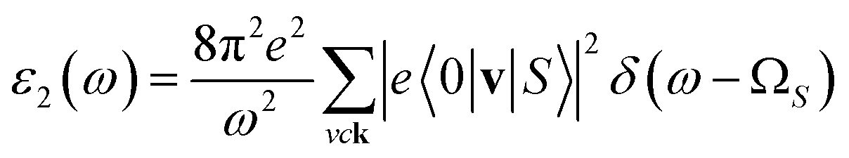
The density functional theory46via the Vienna Ab initio Simulation Package (VASP)47 is utilized to investigate the optimal geometric structure and electronic and optical properties of 2D group III-nitride materials. The Perdew–Burke–Ernzerhof generalized gradient approximation was used for the exchange-correlation functions.48–51 The projector-augmented wave method52 was utilized for the characterization of the ion and valence electron interactions. The unit cells of these monolayers are built with a vacuum region larger than 16 Å to avoid spurious interactions. The cutoff energy for the expansion of the plane wave basis was set to 500 eV. The Brillouin zone was integrated with a special k-point mesh of 200 × 200 × 1 in the Γ-centered sampling technique for structural optimization.53 The convergence condition of the ground state is set to be 10−8 eV between two consecutive simulation steps, and all atoms could fully relax during the geometric optimization until the Hellmann–Feynman force acting on each atom was smaller than 0.01 eV. The Heyd–Scuseria–Ernzerhof hybrid-function (HSE06) method54 is added to get more band gaps. To evaluate the dynamic stability of group III–V systems, phonon energy dispersions were calculated within the harmonic approximations by using density functional perturbation theory as implemented in the PHONOPY code.55 In these calculations, at least five neighboring interactions (corresponding to a 5 × 5 × 1 supercell) have been taken into account to get a reliable phonon band structure.On top of DFT wave functions, the quasi-particle energies are obtained within approximation for the self-energy, the cutoff energy for the response function was set to 300 eV, and 60 × 60 × 1 Γ-centered point sampling was used to represent reciprocal space. The Wannier interpolation procedure performed in the WANNIER90 code56 was used to plot the accurate GW standard. The single particle excitation spectra, which are related to the imaginary part of the dielectric functions ε2(ω), could be described by the following Fermi's golden role:57
 | (1) |
In addition to the single-particle excitations, the presence of stable excitons may strongly affect the optical properties. To evaluate this bound state of the electron–hole pair, we solve the standard BSE.58
 | (2) |
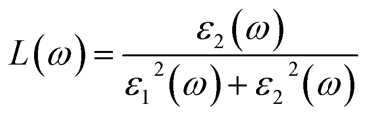
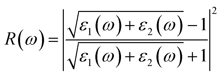
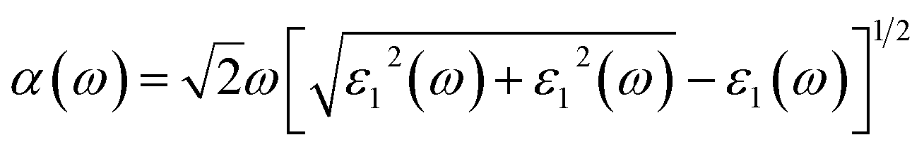
Note that the k-point sampling, energy cutoff, and number of bands were set to the same values as in the GW level. The close connection of the initial and the final orbital hybridizations with the prominence of optical excitations, and the effects of the electron–hole couplings on the optical properties are the main study foci of the current work. Other optical properties, such as the energy loss functions,59 absorption coefficient,60 reflectivity,61 refractive index, and extinction coefficient can be obtained from the dielectric function using the following equations:
 | (3) |
 | (4) |
 | (5) |
3 Results and discussion
Fig. 1a–d indicate the optimal structures of 2D BN, AlN, GaN, and InN monolayers. The optimized lattice constants are equal to 2.51 Å, 3.13 Å, 3.25 Å, and 3.64 Å, respectively (Table 1). These values are suitable for previous studies.34,62 Similar to that of graphene, the unit cell of these materials possesses two atoms; the top view presents a honeycomb lattice, while the side view exhibits a planar structure with the height difference between two sub-lattices equalling zero, thus, leading to impure sp2 bonding configurations. The B–N, Al–N, Ga–N, and In–N bond lengths are equal to 1.45 Å, 1.81 Å, 1.88 Å, and 2.10 Å, respectively, which agree well with previous studies.10,63 Similar to that of graphene,64 group III–V honeycomb lattices are constructed by the rather strong impure σ bonding, while the impure π bonds due to the impure pz orbital hybridizations are rather weak and well separated from the σ ones. Even though they have a similar structure, the electronic and optical properties of group III–V materials are predicted to be rather different from that of graphene due to the presence of impure orbital hybridizations, and the broken hexagon symmetry. Information about the optimal geometric properties of group III–V two-dimensional materials could be detected by high-precision measurements, e.g., the side and top views of the graphene-like materials can be tested by using tunneling electron microscopy (TEM)65,66 and scanning tunneling microscopy (STM),67 respectively.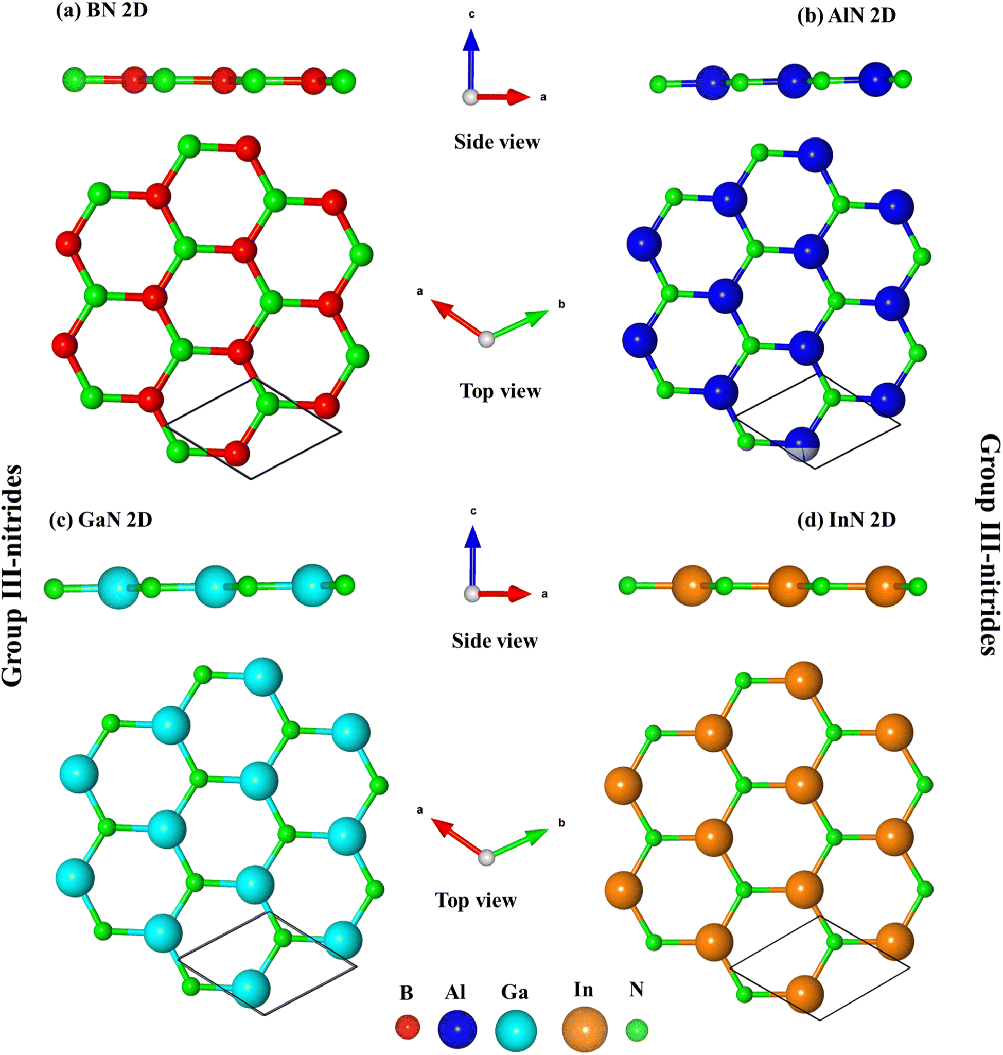 | ||
| Fig. 1 (a–d) Side view and top view for BN, AlN, GaN, and InN monolayers, respectively. The solid black is a unit cell with two atoms. The red, blue, cyan, yellow, and green balls represent by B, Al, Ga, In, and N atoms. | ||
| Materials | Lattice constants (Å) | Energy gap (eV) | |||
|---|---|---|---|---|---|
| DFT | DFT + SOC | HSE | GW | ||
| a Ref. 68. b Ref. 34. c Ref. 69. d Ref. 10. e Ref. 44. f Ref. 10. g Ref. 45. h Ref. 70. | |||||
| BN | 2.51 | 4.22 | 4.46 | 5.71 | 6.44 |
| 2.50a | 4.65e | 5.70e | 6.86f | ||
| 6.10h | |||||
| AlN | 3.13 | 2.84 | 2.87 | 4.02 | 5.18 |
| 3.12b | 2.91e | 4.04e | 5.57f | ||
| 5.80h | |||||
| GaN | 3.25 | 1.89 | 1.90 | 3.19 | 4.32 |
| 3.19c | 2.16e | 3.44e | 4.10g | ||
| 3.50h | |||||
| InN | 3.64 | 0.35 | 0.35 | 1.51 | 1.41 |
| 3.57d | 0.56e | 1.53e | 1.70g | ||
To verify the dynamic stability, the phonon energy dispersion of the studied materials has been calculated and shown in Fig. 2a–d. The phonon band structure of group III-nitride monolayers shows six phonon branches since their unit cells possess two atoms. According to the vibration of atoms along the long wavelength limit, the phonon energy sub-bands could be classified into three acoustic modes (vibrations of atoms with the same phase) and three optic modes (vibrations of atoms with the opposite phase). The transverse acoustic (TA) and longitudinal acoustic (LA) phonon branches of BN, AlN, GaN, and InN monolayers present linear dispersion which satisfies the Debye model, while the out-of-plane acoustic modes (ZA) exhibit a quadratic form which is the main characteristic of two-dimensional materials.71 The crossing behavior of the in-plane and out-of-plane phonon branches indicated the well-separated nature of the former and the latter and reflected the planar nature of the group III–V materials. Another intriguing feature is the presence of an obvious phonon gap. The presence of this large acoustic-optical phonon spacing originated from the atomic mass difference in the unit cell. In general, the phonon band gap of group III–V monolayers which can describe the difference between low-frequency acoustic and high-frequency optic branches could be classified in the following order: BN (1.0 THz), AlN (5.0 THz), GaN (10.5 THz), and InN (11.5 THz) as expected. Such a frequency gap is a typical feature of phonon transport in group-III nitride semiconductors72 and also denoted the absence of phonon scattering between optical (except the ZO branch) and acoustic branches. Important properties we would like to emphasize are the absence of imaginary frequencies in the phonon spectra, and thus, all studied two-dimensional materials are dynamically stable. As shown in Fig. 3a–d, the corresponding phonon density of states reveals that B/Al/Ga/In atoms are the principal contributors to the low-frequency acoustic branches but the high-frequency optical modes are mostly dominated by the N atoms. More importantly, the vanishing frequencies between the optic mode and acoustic branch states of these materials, which are increased, are equal to phonon band gaps. Consequently, the remarkable chemical tunability and orbital interactions of N atoms will drastically alter phonon characteristics and have the potential to greatly reduce lattice thermal conductivity.
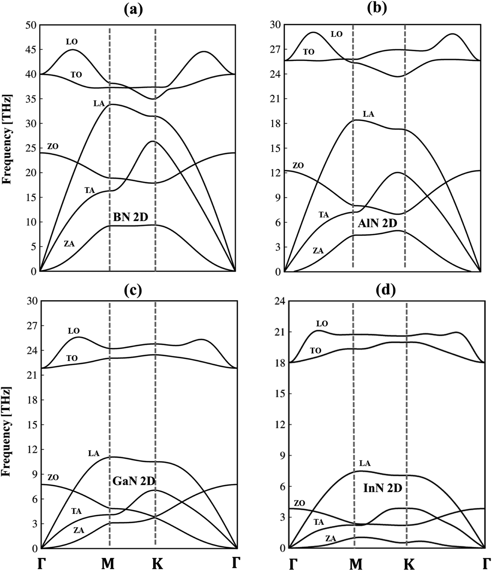 | ||
| Fig. 2 Phonon dispersion curves are calculated for (a) BN, (b) AlN, (c) GaN, and (d) InN monolayers, respectively. Note that LA, TA, and ZA are longitudinal, transverse, and out-of-plane acoustic branches and LO, TO, and ZO, are longitudinal, transverse, and out-of-plane optic modes. | ||
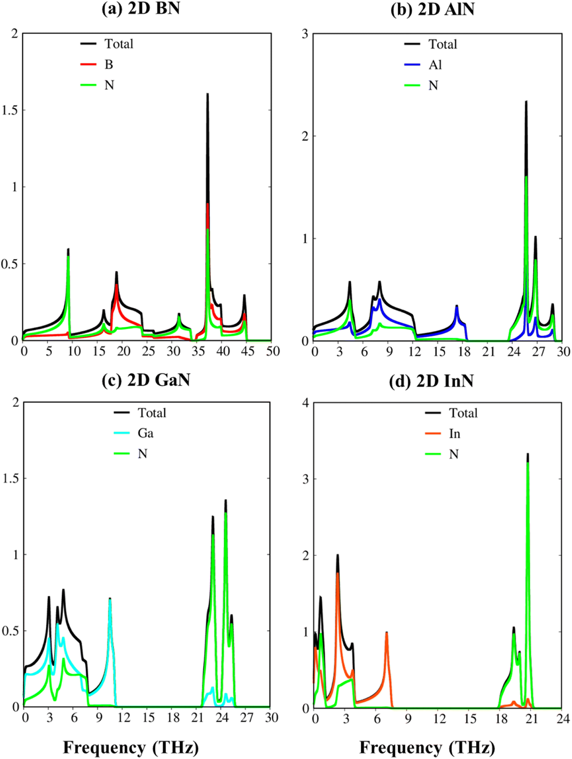 | ||
| Fig. 3 The vibrational atom-dominant density of states, corresponding to the phonon bands of (a) BN, (b) AlN, (c) GaN, and (d) InN monolayers. | ||
The electronic band structures of group III–V monolayers are shown in Fig. 4 and 5a–d with an effective range within the interval of −20.0 eV to 14.0 eV. There are four energy sub-bands in the occupied states which are related to the four active orbitals. The occupied state and the unoccupied one are highly asymmetric to each other around the Fermi level indicating complicated hybridizations. The presence of several critical points, the band edge states with the vanishing of the group velocity, will induce strong Van Hove singularities in the density of states and thus be responsible for the optical excitations. The absence of the linear and isotropic Dirac cone and the presence of a large quasi-particle band gap reflected the broken hexagon symmetry and the presence of the onsite energy differences. The electronic band gap values are calculated at various levels of theories, such as DFT, DFT + spin–orbit coupling (SOC), HSE06, and GW standards, as can be seen in Table 1. These energy gap values match well with those in previous studies. Remarkably, (i) the SOC influences are found to be negligible. (ii) HSE06 calculations modify the exchange energy with portions of the exact exchange, parameterized to ensure agreement with the experiment for specific properties over a specific data set of materials. On the other hand, the GW level goes beyond the mean-field theory and can calculate exact many-body terms of electron–electron interactions.73,74 The order of accuracy is illustrated as GW > HSE > DFT. (iii) More importantly, DFT uses the Kohn–Sham (KS) equation with the single-body method, making it a powerful tool to study ground state properties of condensed matter systems. However, its predictions of a fundamental energy gap are often smaller than experimental observations due to inaccurate exchange-correlation approximations. Therefore, we have used the high-precision GW calculation method to obtain an accurate band structure for these graphene-like monolayers. The observed increase in the electronic band gap can be attributed to the electron–electron self-energy effects, as extensively discussed in numerous prior publications.75–78 The GW gap (called a quasi-particle gap) agrees closely with the electronic gap measured in scanning tunneling spectroscopy (STS) experiments. This means that the GW gap is comparable to the experimental results.
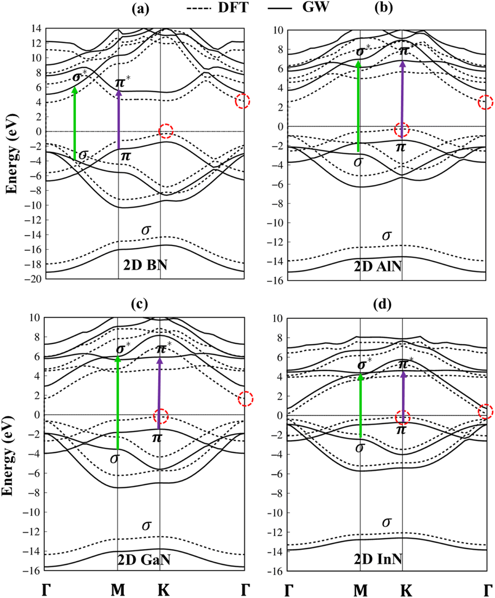 | ||
| Fig. 4 (a–d) Band structures of BN, AlN, GaN, and InN monolayers, corresponding to DFT and GW standards, respectively, denoted by dashed and solid curves. Noted: dashed red circles denote indirect gap semiconductors. Green and purple arrows are vertically excited from occupied states to unoccupied ones in the band structure of the GW level. | ||
The impure π sub-bands, which are governed by 2pz/3pz/4pz/5pz orbitals, starting from the K, get the saddle point at M and end at the Γ. Beyond the π sub-bands, group III–V semiconductors' electronic band structures also present three impure σ energy subbands belonging to the s, px, and py active orbitals. Here, impure σ bonds, which originated from B-2s/Al-3s/Ga-4s/In-5s and N-2s orbitals, appear at the deepest valence band due to the highest ionization energies. The crossing behavior of impure σ and π sub-bands can be observed, which reflects the well separated features of the former and the latter and is associated with the planar nature of the group III–V monolayers.
According to the dominance of specific atoms, the electronic band structure of group III–V materials is also classified into two distinct regions: (i) the B, Al, Ga, In, and N atoms contributed to the entire band structure under the red, blue, cyan, yellow, and green circles (Fig. 5a–d) and nitrogen atoms are mostly in the occupied states. (ii) In contrast, the boron, aluminum, gallium, and indium atoms contributed mainly to unoccupied states of the electronic spectra. These behaviors, which connect with projected atom-/orbital hybridizations in PDOS (Fig. 7a–d discussed later), can provide sufficient information about hybridizations in the chemical bonds.
 | ||
| Fig. 5 (a–d) B, Al, Ga, In, and N atoms of BN, AlN, GaN, and InN two-dimensional monolayers are represented by red, blue, cyan, orange, and green balls, respectively. | ||
The charge density distributions (Fig. 6a–d) and the highest occupied and lowest unoccupied band decompound charge densities could provide useful information to understand the orbital hybridizations in the chemical bonds. As shown in Fig. 6, the B–N, Al–N, Ga–N, and In–N chemical bonds exhibit asymmetric charge density distribution ρ; in particular, charge density is mostly located around the nitrogen atom which is associated with larger ionization energy. The asymmetric charge density also indicated the ionic-covalent nature of the B-/Al-/Ga-/In–N chemical bonds. The band decomposed charge density (Fig. 6) on the right panels indicated that the π bonding attends to the vacuum and is well separated from the σ bonding. Even though impure sp2 hybridizations are present, group III–V monolayers could be classified from graphene via the impure π and impure σ bondings.
 | ||
| Fig. 6 (a–d) Charge density distributions and band decomposed charge densities of the BN, AlN, GaN, and InN monolayers, respectively. The red, blue, cyan, yellow, and green balls are the B, Al, Ga, In, and N atoms. | ||
To fully comprehend the orbital hybridizations in the B–/Al–/Ga–/In–N chemical bonding, the orbital-projected density of states has been established and is displayed in Fig. 7a–d. The strong prominent peaks of van Hove singularities appear in the density of states in the density of states spectra. These prominent peaks mostly present the step functions or the divergence peaks, which have mostly arisen from the parabolic or the flat energy dispersions of two-dimensional systems. These prominent peaks are responsible for the strong optical excitations. The vanishing of the density of states of BN, AlN, GaN, and InN around the Fermi level is, respectively, about 4.22 eV, 2.84 eV, 1.89 eV, and 0.35 eV, which reflect the semiconducting behavior and are consistent with the electronic band structures (DFT level). Very importantly, the density of states of impure π electrons (due to the pz orbitals) and impure σ electrons (owing to the s, px, and py orbitals) is well separated from each other, which confirms the impure sp2 hybridizations of the planar systems.
 | ||
| Fig. 7 (a–d) Van Hove singularities of the density of states (DOS) and project-density of states (PDOS) of the BN, AlN, GaN, and InN monolayers, respectively, and those coming from B-/Al-/Ga-/In-/N- orbitals (red, blue, cyan, yellow, and green curves), as well as B-(2s, 2px, 2py, and 2pz), Al-(3s, 3px, 3py, and 3pz), Ga-(4s, 4px, 4py, and 4pz), In-(5s, 5px, 5py, and 5pz), and N-(2s, 2px, 2py, and 2pz) orbitals (red, green, blue and cyan curves). | ||
When two-dimensional materials are perturbed by a transverse electromagnetic wave or photon beam, the electrons in the occupied states are vertically promoted to unoccupied states. All the charge carriers in two-dimensional systems will dynamically screen this external field and create induced current density and, thus, charge density fluctuations. The complex dielectric functions can provide useful information to fully comprehend optical transition mechanisms. The close connection between the initial and the final orbital characters and the prominent peaks in the optical absorbance spectra are the most concerning aspects of the current work.
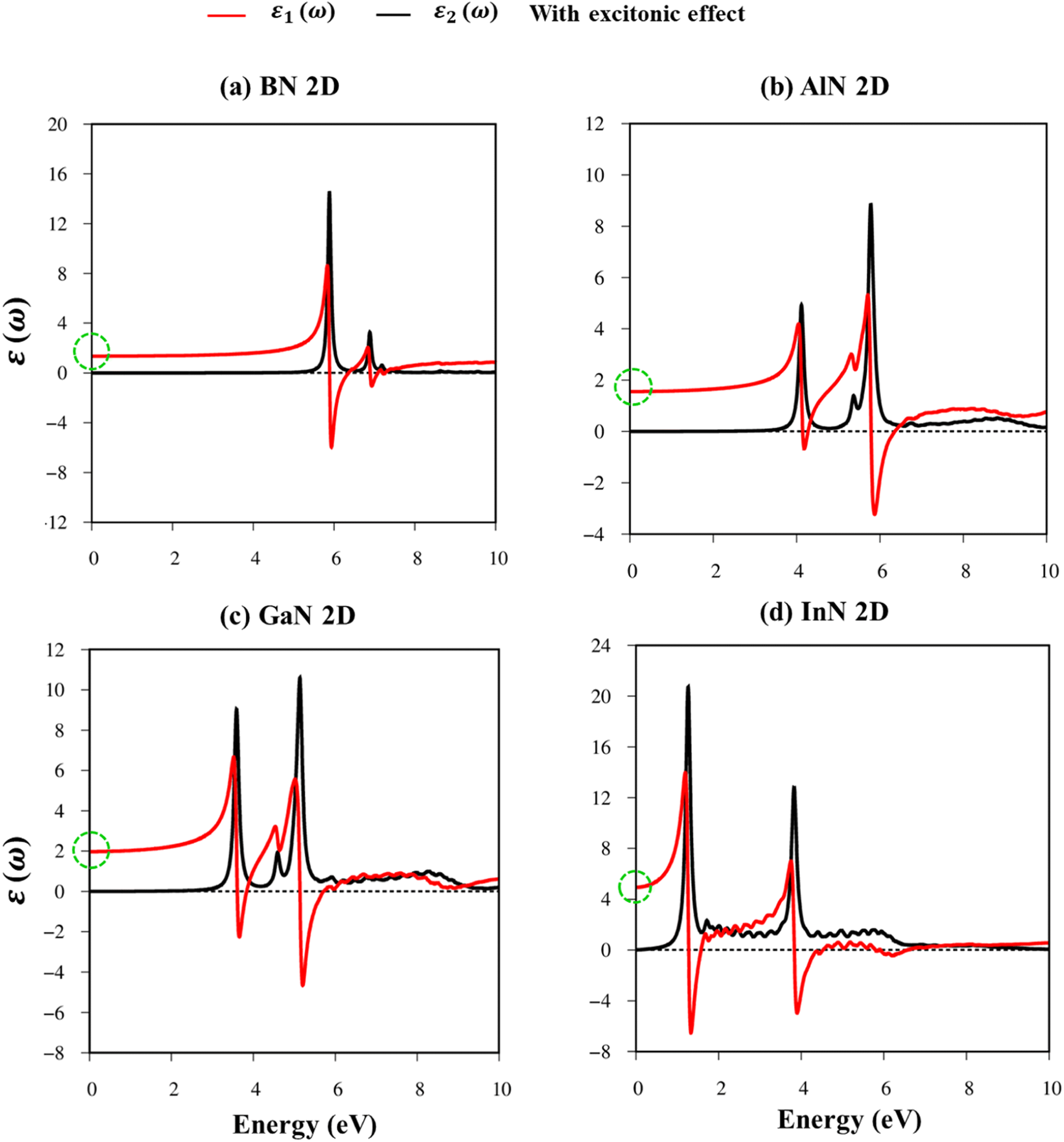
Fig. 8a–d indicate the imaginary part of the dielectric functions ε2(ω) in the presence (absence) of excitonic effects, which are represented by red (black) curves. The optical absorbance spectra of group III–V materials exhibit two prominent peaks which arise from the specific Van Hove singularities; e.g., the BN monolayer exhibits two prominent peaks at 8.50 eV and 9.50 eV, which are due to the excitations of π → π*, and σ → σ* states at the K and M critical points, respectively (Fig. 8a). Such identification could be achieved by the delicate connection between the projected density of states and the prominent excitations, that is, the strong Van Hove singularities will induce large optical excitation peaks. As a consequence, the orbital hybridizations related to optical responses are indicated in Tables 2–5, while the vertical excitations that connect the occupied states to the unoccupied ones in the quasi-band structures are shown in Fig. 4a–d. The optical gap (E0g) at the threshold frequency is about 7.10 eV, 5.80 eV, 5.10 eV, and 1.41 eV for the BN, AlN, GaN, and InN monolayers, respectively, which are consistent with the sizable-large gap of two-dimensional semiconductors. In addition to the optical gap, the extra prominent peaks (E1, E2, and E3) exhibit significant redshifts when the electron–hole interactions (excitons) are taken into account, e.g., about 1.30 eV, 1.25 eV, 0.90 eV, and 0.40 eV for the optical gap of the BN, AlN, GaN and InN monolayers, suggesting strong energy bindings/robust excitonic effects. Such a large change in the optical spectrum indicated that the excitonic effects are significant and the electron–hole bound states may survive at high temperatures. The strong electron–hole bound states originated from the insignificant electronic screening (large electronic band gap and small ε1(0) in Fig. 9a–d) and the absence of vertical electronic screening due to the quantum confinement effects. The zero points in dielectric functions, respectively 7.5 eV, 6.5 eV, 9.2 eV, and 6.8 eV for two-dimensional BN, AlN, GaN, and InN monolayers are equal to plasmon mode in energy loss functions (discussed later in Fig. 10). On the other hand, the real part ε1(ω) and the imaginary part ε2(ω) of dielectric functions are connected by using the Kramers–Kronig relationship,79 which leads to the appearance of prominent peaks simultaneously as can be seen in Fig. 9a–d. It is interesting to note that there exists an inverse relationship between the band gap energy values (Eg) and the dielectric constants (ε1(0)) in various monolayers80 ranging from BN to InN. Specifically, from BN to InN monolayers, the values of band gap energy decreased while the values of dielectric constant increased. For instance, the band gap energy values for 2D BN, AlN, GaN, and InN monolayers are 6.44 eV, 5.18 eV, 4.32 eV, and 1.41 eV, respectively, while their corresponding dielectric constant values are 1.6, 1.8, 2.0, and 4.8.
 | ||
| Fig. 8 (a–d) The imaginary part of the dielectric functions with and without exciton effects (red and black curves, respectively) of the BN, AlN, GaN, and InN monolayers, respectively. The dashed vertical greens correspond to the energy gap at the GW level. | ||
| Energy (eV) | Label | Distinct colors | Orbital hybridizations in B–N bonds |
|---|---|---|---|
| 5.50 | E1 | ||
| 6.80 | E2 | Threshold frequency | |
| 7.10 | E3 | ||
| 8.50 | Purple | 2pz–2pz | |
| 9.50 | Green | 2px, 2py–2px, and 2py |
| Energy (eV) | Label | Distinct colors | Orbital hybridizations in Al–N bonds |
|---|---|---|---|
| 4.10 | E1 | ||
| 5.35 | E2 | Threshold frequency | |
| 5.80 | E3 | ||
| 8.30 | Purple | 3pz–2pz | |
| 9.30 | Green | 3px, 3py–2px, and 2py |
| Energy (eV) | Label | Distinct colors | Orbital hybridizations in Ga–N bonds |
|---|---|---|---|
| 3.60 | E1 | ||
| 4.50 | E2 | Threshold frequency | |
| 5.10 | E3 | ||
| 7.30 | Purple | 4pz–2pz | |
| 8.80 | Green | 4px, 4py–2px, and 2py |
| Energy (eV) | Label | Distinct colors | Orbital hybridizations in the In–N bonds |
|---|---|---|---|
| 1.20 | E1 | ||
| 1.60 | E2 | Threshold frequency | |
| 3.80 | E3 | ||
| 5.30 | Purple | 5pz–2pz | |
| 6.80 | Green | 5px, 5py–2px, and 2py |
 | ||
| Fig. 9 (a–d) The real part and imaginary part of the dielectric functions with exciton effects (red and black curves, respectively) of the BN, AlN, GaN, and InN monolayers, respectively. The dashed green circles correspond to dielectric constants. | ||
 | ||
| Fig. 10 (a–d) Reflectance spectra, energy loss functions, and absorbance spectra in the presence of an excitonic effect, respectively for the BN, AlN, GaN, and InN monolayers. | ||
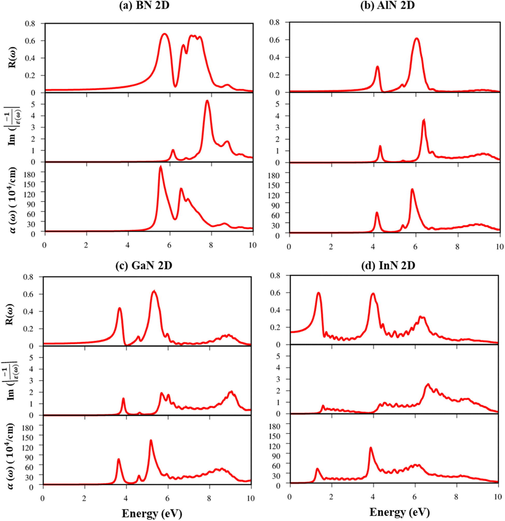
The energy loss function (ELF), being determined using the  , could provide useful information about the collective charge excitations. Each prominent peak in the ELF will denote a plasmon mode, the quantization of the collective excitation. The ELF of group III-nitride monolayers (Fig. 10) exhibits two prominent excitation peaks similar to that of graphene, e.g., 4.0 eV and 7.8 eV for the BN monolayer; the former belongs to the coherent excitation of the impure π charges (B-2pz and N-2pz), while the latter is related to the excitation of all carriers in the low-dimensional systems. It is very important to note that the low-frequency plasmon due to the free charge is absent in BN two-dimensional semiconductors. The other optical properties such as absorbance α(ω) and reflectance R(ω) are also calculated and shown in Fig. 10. The reflectivity R(ω) is weakly dependent on frequency when a photon frequency is smaller than the onset frequency, whereas the absorption coefficient α(ω) disappears owing to the absence of the electronic excitation contribution. Beyond the threshold frequency, both α(ω) and R(ω) are changing significantly and sensitively in the excitation model. The diverse inter-band transitions are responsible for the rapid increase in the absorption coefficient. The inverse values of the absorption coefficient are equal to 50.0 Å, 150.0 Å, 130.0 Å, and 250.0 Å for the 2D BN, AlN, GaN, and InN monolayers, respectively, indicating that the photon energy propagating in the medium is easily absorbed by the electronic excitations.
The examination of the rich and unique electronic and optical properties of group III–V materials required high-resolution equipment. For instance, the electronic band structure including various energy dispersions can be depicted by using ARPES81 measurement, and the STS82 examination can provide asymmetric or shoulder Van Hove singularities around the Fermi level. Being supported by Kramers–Kronig relations,79 the results of the adsorption, reflection, or transmission measurements can be compared with our absorption, reflection coefficients, and energy loss functions. Other information, such as diversified optical excitation peaks, the slight redshift of the optical gap due to the excitonic effect, and the strong anisotropy of the optical responses can be obtained. Our analysis of orbital hybridizations that are related to optical properties is very difficult to achieve in experiments.
4 Conclusions
To summarize, this study employs first-principles calculations to analyze the electronic and optical properties of group III-nitride monolayers. Here, the studied materials exhibit rich and unique geometric, electronic, and optical properties. Similar to graphene, these systems also exhibit planar and uniform hexagonal honeycomb structures. Also, sizable electronic indirect band gaps in semiconductors and insulators of 4.22 (6.44 eV), 2.84 eV (5.18 eV), 1.89 eV (4.32), and 0.35 eV (2.43) for DFT (GW) approximations were found in BN, AlN, GaN and InN monolayers, respectively. The charge density, the band decomposed charge density, and the Van Hove singularities in the density of states are reflected in the main orbital characters of the concerned materials. In addition, these monolayers belong to impure sp2 hybridizations which are due to the orbital hybridizations of impure π and impure σ orbitals.More importantly, these graphene-like materials demonstrate distinctive and diverse optical properties, characterized by strong excitonic effects, and were able to establish a correlation between the initial and final states of orbital hybridizations and the prominent excitation peaks observed in the optical spectra. Moreover, these monolayers exhibit low reflectance spectra, high absorption coefficients, and distinctive plasmon modes in the energy loss functions, further highlighting their unique optical properties.
In short, our study provided valuable insights into the physical and chemical characteristics. These findings are of significant interest and suggest that these materials could be useful for a broad range of applications. Moreover, the theoretical framework used in this research can be extended to analyze other graphene-like and emerging materials, thereby opening new avenues for future research.
Conflicts of interest
The authors declare no competing interests.Acknowledgements
T.-R. C. was supported by the 2030 Cross-Generation Young Scholars Program from the National Science and Technology Council (NSTC) in Taiwan (Program No. MOST111-2628-M-006-003-MY3), National Cheng Kung University (NCKU), Taiwan, and the National Center for Theoretical Sciences, Taiwan. This research was supported, in part, by the Higher Education Sprout Project, Ministry of Education to the Headquarters of University Advancement at NCKU. M.-F. L. was supported by the Hierarchical Green-Energy Materials (Hi-GEM) Research Center, from the Featured Areas Research Center Program within the framework of the Higher Education Sprout Project by the Ministry of Education (MOE) and the Ministry of Science and Technology (MOST 111-2112-M-006-020) in Taiwan.References
- A. Chaves, et al., Bandgap engineering of two-dimensional semiconductor materials, npj 2D Mater. Appl., 2020, 4(1), 1–21 CrossRef.
- X.-Y. Lin, F.-S. Meng, Q.-C. Liu, Q. Xue and H. Zhang, Semiconducting two-dimensional group VA–VA haeckelite compounds with superior carrier mobility, Phys. Chem. Chem. Phys., 2020, 22(21), 12260–12266 RSC.
- R. Dong, et al., A coronene-based semiconducting two-dimensional metal-organic framework with ferromagnetic behavior, Nat. Commun., 2018, 9(1), 1–9 CrossRef CAS PubMed.
- E. J. Duplock, M. Scheffler and P. J. Lindan, Hallmark of perfect graphene, Phys. Rev. Lett., 2004, 92(22), 225502 CrossRef PubMed.
- J.-T. Wang, C. Chen, E. Wang and Y. Kawazoe, A new carbon allotrope with six-fold helical chains in all-sp2 bonding networks, Sci. Rep., 2014, 4(1), 1–5 Search PubMed.
- M. Kan, et al., Structures and phase transition of a MoS2 monolayer, J. Phys. Chem. C, 2014, 118(3), 1515–1522 CrossRef CAS.
- S. Zhao, J. Xue and W. Kang, Gas adsorption on MoS2 monolayer from first-principles calculations, Chem. Phys. Lett., 2014, 595, 35–42 CrossRef.
- D. Wickramaratne, L. Weston and C. G. Van de Walle, Monolayer to Bulk Properties of Hexagonal Boron Nitride, J. Phys. Chem. C, 2018, 122(44), 25524–25529, DOI:10.1021/acs.jpcc.8b09087.
- L. Karvonen, et al., Investigation of Second- and Third-Harmonic Generation in Few-Layer Gallium Selenide by Multiphoton Microscopy, Sci. Rep., 2015, 5(1), 10334, DOI:10.1038/srep10334.
- H. Şahin, et al., Monolayer honeycomb structures of group-IV elements and III–V binary compounds: First-principles calculations, Phys. Rev. B: Condens. Matter Mater. Phys., 2009, 80(15), 155453 CrossRef.
- I. Datta, et al., Low-loss composite photonic platform based on 2D semiconductor monolayers, Nat. Photonics, 2020, 14(4), 256–262 CrossRef CAS.
- Z. Hu, Y. Ding, X. Hu, W. Zhou, X. Yu and S. Zhang, Recent progress in 2D group IV–IV monochalcogenides: synthesis, properties and applications, Nanotechnology, 2019, 30(25), 252001 CrossRef CAS PubMed.
- M. Causa, R. Dovesi and C. Roetti, Pseudopotential Hartree-Fock study of seventeen III–V and IV–IV semiconductors, Phys. Rev. B: Condens. Matter Mater. Phys., 1991, 43(14), 11937 CrossRef CAS PubMed.
- Q. Peng, W. Ji and S. De, Mechanical properties of the hexagonal boron nitride monolayer: Ab initio study, Comput. Mater. Sci., 2012, 56, 11–17 CrossRef CAS.
- T. T. Tran, K. Bray, M. J. Ford, M. Toth and I. Aharonovich, Quantum emission from hexagonal boron nitride monolayers, Nat. Nanotechnol., 2016, 11(1), 37–41 CrossRef CAS PubMed.
- Y. Bai, K. Deng and E. Kan, Electronic and magnetic properties of an AlN monolayer doped with first-row elements: a first-principles study, RSC Adv., 2015, 5(24), 18352–18358 RSC.
- D. V. Fakhrabad, N. Shahtahmasebi and M. Ashhadi, Optical excitations and quasiparticle energies in the AlN monolayer honeycomb structure, Superlattices Microstruct., 2015, 79, 38–44 CrossRef.
- T. Hu, X. Mei, Y. Wang, X. Weng, R. Liang and M. Wei, Two-dimensional nanomaterials: fascinating materials in biomedical field, Sci. Bull., 2019, 64(22), 1707–1727 CrossRef CAS PubMed.
- N. Izyumskaya, D. O. Demchenko, S. Das, Ü. Özgür, V. Avrutin and H. Morkoç, Recent development of boron nitride towards electronic applications, Adv. Electron. Mater., 2017, 3(5), 1600485 CrossRef.
- M. Li, et al., Perspectives on environmental applications of hexagonal boron nitride nanomaterials, Nano Today, 2022, 44, 101486 CrossRef CAS.
- F. Yang, et al., 2D organic materials for optoelectronic applications, Adv. Mater., 2018, 30(2), 1702415 CrossRef PubMed.
- J. Chen, et al., III–VI van der Waals heterostructures for sustainable energy related applications, Nanoscale, 2019, 11(13), 6431–6444 RSC.
- K. K. Kim, et al., Synthesis of monolayer hexagonal boron nitride on Cu foil using chemical vapor deposition, Nano Lett., 2012, 12(1), 161–166 CrossRef PubMed.
- R. Y. Tay, et al., Synthesis of aligned symmetrical multifaceted monolayer hexagonal boron nitride single crystals on resolidified copper, Nanoscale, 2016, 8(4), 2434–2444 RSC.
- L. Schué, et al., Dimensionality effects on the luminescence properties of hBN, Nanoscale, 2016, 8(13), 6986–6993 RSC.
- C. Bacaksiz, H. Sahin, H. Ozaydin, S. Horzum, R. T. r. Senger and F. M. Peeters, Hexagonal AlN: Dimensional-crossover-driven band-gap transition, Phys. Rev. B: Condens. Matter Mater. Phys., 2015, 91(8), 085430 CrossRef.
- K. Ueda, Y. Tsuchida, N. Hagura, F. Iskandar, K. Okuyama and Y. Endo, High performance of GaN thin films grown on sapphire substrates coated with a silica-submicron-sphere monolayer film, Appl. Phys. Lett., 2008, 92(10), 101101 CrossRef.
- V. Kumaresan, et al., Epitaxy of GaN nanowires on graphene, Nano Lett., 2016, 16(8), 4895–4902 CrossRef CAS PubMed.
- X. Sun, et al., Adsorption of gas molecules on graphene-like InN monolayer: A first-principle study, Appl. Surf. Sci., 2017, 404, 291–299 CrossRef CAS.
- L. H. Li, Y. Chen, G. Behan, H. Zhang, M. Petravic and A. M. Glushenkov, Large-scale mechanical peeling of boron nitride nanosheets by low-energy ball milling, J. Mater. Chem., 2011, 21(32), 11862–11866 RSC.
- J. N. Coleman, et al., Two-dimensional nanosheets produced by liquid exfoliation of layered materials, Science, 2011, 331(6017), 568–571 CrossRef CAS PubMed.
- D. Pierucci, et al., Van der Waals epitaxy of two-dimensional single-layer h-BN on graphite by molecular beam epitaxy: Electronic properties and band structure, Appl. Phys. Lett., 2018, 112(25), 253102 CrossRef.
- D. J. Scalapino, S. R. White and S. Zhang, Insulator, metal, or superconductor: The criteria, Phys. Rev. B: Condens. Matter Mater. Phys., 1993, 47(13), 7995 CrossRef PubMed.
- P. Tsipas, et al., Evidence for graphite-like hexagonal AlN nanosheets epitaxially grown on single crystal Ag (111), Appl. Phys. Lett., 2013, 103(25), 251605 CrossRef.
- R. Beiranvand and S. Valedbagi, Electronic and optical properties of advance semiconductor materials: BN, AlN and GaN nanosheets from first principles, Optik, 2016, 127(3), 1553–1560 CrossRef CAS.
- H. Shu, X. Niu, X. Ding and Y. Wang, Effects of strain and surface modification on stability, electronic and optical properties of GaN monolayer, Appl. Surf. Sci., 2019, 479, 475–481 CrossRef CAS.
- A. G. Bhuiyan, A. Hashimoto and A. Yamamoto, Indium nitride (InN): A review on growth, characterization, and properties, J. Appl. Phys., 2003, 94(5), 2779–2808 CrossRef CAS.
- V. Polyakov, F. Schwierz, F. Fuchs, J. Furthmüller and F. Bechstedt, Low-field and high-field electron transport in zinc blende InN, Appl. Phys. Lett., 2009, 94(2), 022102 CrossRef.
- V. Y. Davydov, et al., Absorption and emission of hexagonal InN. Evidence of narrow fundamental band gap, Phys. Status Solidi B, 2002, 229(3), r1–r3 CrossRef CAS.
- J. Wu, et al., Unusual properties of the fundamental band gap of InN, Appl. Phys. Lett., 2002, 80(21), 3967–3969 CrossRef CAS.
- E. Bellotti, B. K. Doshi, K. F. Brennan, J. D. Albrecht and P. P. Ruden, Ensemble Monte Carlo study of electron transport in wurtzite InN, J. Appl. Phys., 1999, 85(2), 916–923 CrossRef CAS.
- B. E. Foutz, S. K. O'Leary, M. S. Shur and L. F. Eastman, Transient electron transport in wurtzite GaN, InN, and AlN, J. Appl. Phys., 1999, 85(11), 7727–7734 CrossRef CAS.
- K. Chang, et al., Characterizations of InN films on Si (111) substrate grown by metal-organic chemical vapor deposition with a predeposited In layer and a two-step growth method, J. Vac. Sci. Technol., A, 2007, 25(4), 701–705 CrossRef CAS.
- I. Guilhon, D. S. Koda, L. G. Ferreira, M. Marques and L. K. Teles, Approximate quasiparticle correction for calculations of the energy gap in two-dimensional materials, Phys. Rev. B, 2018, 97(4), 045426 CrossRef CAS.
- M. S. Prete, A. Mosca Conte, P. Gori, F. Bechstedt and O. Pulci, Tunable electronic properties of two-dimensional nitrides for light harvesting heterostructures, Appl. Phys. Lett., 2017, 110(1), 012103 CrossRef.
- K. Burke, Perspective on density functional theory, J. Chem. Phys., 2012, 136(15), 150901 CrossRef PubMed.
- J. Hafner, Ab-initio simulations of materials using VASP: Density-functional theory and beyond, J. Comput. Chem., 2008, 29(13), 2044–2078 CrossRef CAS PubMed.
- J. P. Perdew, K. Burke and Y. Wang, Generalized gradient approximation for the exchange-correlation hole of a many-electron system, Phys. Rev. B: Condens. Matter Mater. Phys., 1996, 54(23), 16533 CrossRef CAS PubMed.
- H. Peng and J. P. Perdew, Rehabilitation of the Perdew-Burke-Ernzerhof generalized gradient approximation for layered materials, Phys. Rev. B, 2017, 95(8), 081105 CrossRef.
- G. K. Madsen, Functional form of the generalized gradient approximation for exchange: The PBE α functional, Phys. Rev. B: Condens. Matter Mater. Phys., 2007, 75(19), 195108 CrossRef.
- S. N. Maximoff, M. Ernzerhof and G. E. Scuseria, Current-dependent extension of the Perdew–Burke–Ernzerhof exchange-correlation functional, J. Chem. Phys., 2004, 120(5), 2105–2109 CrossRef CAS PubMed.
- P. E. Blöchl, Projector augmented-wave method, Phys. Rev. B: Condens. Matter Mater. Phys., 1994, 50(24), 17953 CrossRef PubMed.
- D. J. Chadi and M. L. Cohen, Special points in the Brillouin zone, Phys. Rev. B: Solid State, 1973, 8(12), 5747 CrossRef.
- J. Heyd, J. E. Peralta, G. E. Scuseria and R. L. Martin, Energy band gaps and lattice parameters evaluated with the Heyd-Scuseria-Ernzerhof screened hybrid functional, J. Chem. Phys., 2005, 123(17), 174101 CrossRef PubMed.
- A. Togo, First-principles Phonon Calculations with Phonopy and Phono3py, J. Phys. Soc. Jpn., 2023, 92(1), 012001 CrossRef.
- G. Pizzi, et al., Wannier90 as a community code: new features and applications, J. Phys.: Condens. Matter, 2020, 32(16), 165902 CrossRef CAS PubMed.
- A. Crépieux and P. Bruno, Theory of the anomalous Hall effect from the Kubo formula and the Dirac equation, Phys. Rev. B: Condens. Matter Mater. Phys., 2001, 64(1), 014416 CrossRef.
- J. Vinson, J. Rehr, J. Kas and E. Shirley, Bethe-Salpeter equation calculations of core excitation spectra, Phys. Rev. B: Condens. Matter Mater. Phys., 2011, 83(11), 115106 CrossRef PubMed.
- T. Nagatomi, R. Shimizu and R. Ritchie, Energy loss functions for electron energy loss spectroscopy, Surf. Sci., 1999, 419(2–3), 158–173 CrossRef CAS.
- S.-I. Thomasson, On the absorption coefficient, Acta Acust. Acust., 1980, 44(4), 265–273 Search PubMed.
- S. Mallick and L. N. Frazer, Practical aspects of reflectivity modeling, Geophysics, 1987, 52(10), 1355–1364 CrossRef.
- M. Huda and L. Kleinman, h-BN monolayer adsorption on the Ni (111) surface: A density functional study, Phys. Rev. B: Condens. Matter Mater. Phys., 2006, 74(7), 075418 CrossRef.
- C. Xia, Y. Peng, S. Wei and Y. Jia, The feasibility of tunable p-type Mg doping in a GaN monolayer nanosheet, Acta Mater., 2013, 61(20), 7720–7725 CrossRef CAS.
- V. K. Dien, W.-B. Li, K.-I. Lin, N. T. Han and M.-F. Lin, Electronic and optical properties of graphene, silicene, germanene, and their semi-hydrogenated systems, RSC Adv., 2022, 12(54), 34851–34865 RSC.
- N. Alem, R. Erni, C. Kisielowski, M. D. Rossell, W. Gannett and A. Zettl, Atomically thin hexagonal boron nitride probed by ultrahigh-resolution transmission electron microscopy, Phys. Rev. B: Condens. Matter Mater. Phys., 2009, 80(15), 155425 CrossRef.
- A. Aiello, et al., Deep ultraviolet luminescence due to extreme confinement in monolayer GaN/Al (Ga) N nanowire and planar heterostructures, Nano Lett., 2019, 19(11), 7852–7858 CrossRef CAS PubMed.
- R. J. P. Román, et al., Band gap measurements of monolayer h-BN and insights into carbon-related point defects, 2D Materials, 2021, 8(4), 044001 CrossRef.
- W. Auwärter, T. Kreutz, T. Greber and J. Osterwalder, XPD and STM investigation of hexagonal boron nitride on Ni (111), Surf. Sci., 1999, 429(1–3), 229–236 CrossRef.
- A. Smith, R. Feenstra, D. Greve, J. Neugebauer and J. Northrup, Reconstructions of the GaN (000 1) surface, Phys. Rev. Lett., 1997, 79(20), 3934 CrossRef CAS.
- D. Vogel, P. Krüger and J. Pollmann, Structural and electronic properties of group-III nitrides, Phys. Rev. B: Condens. Matter Mater. Phys., 1997, 55(19), 12836 CrossRef CAS.
- A. Taheri, S. Pisana and C. V. Singh, Importance of quadratic dispersion in acoustic flexural phonons for thermal transport of two-dimensional materials, Phys. Rev. B, 2021, 103(23), 235426 CrossRef CAS.
- L. Lindsay, D. Broido and T. Reinecke, Ab initio thermal transport in compound semiconductors, Phys. Rev. B: Condens. Matter Mater. Phys., 2013, 87(16), 165201 CrossRef.
- M. Shishkin and G. Kresse, Implementation and performance of the frequency-dependent G W method within the PAW framework, Phys. Rev. B: Condens. Matter Mater. Phys., 2006, 74(3), 035101 CrossRef.
- L. C. Lentz and A. M. Kolpak, Predicting HSE band gaps from PBE charge densities via neural network functionals, J. Phys.: Condens. Matter, 2020, 32(15), 155901 CrossRef CAS PubMed.
- N. Thi Han, V. Khuong Dien and M.-F. Lin, Electronic and optical properties of CsGeX3 (X= Cl, Br, and I) compounds, ACS Omega, 2022, 7(29), 25210–25218 CrossRef CAS PubMed.
- N. T. Han, V. K. Dien and M.-F. Lin, Electronic and optical properties of CH3NH3SnI3 and CH (NH2) 2SnI3 perovskite solar Cell, Phys. Status Solidi RRL, 2023, 2300020 CrossRef CAS.
- N. T. Han, V. K. Dien and M.-F. Lin, Excitonic effects in the optical spectra of Li2SiO3 compound, Sci. Rep., 2021, 11(1), 7683 CrossRef CAS PubMed.
- V. K. Dien, N. T. Han, W.-P. Su and M.-F. Lin, Spin-dependent optical excitations in LiFeO2, ACS Omega, 2021, 6(39), 25664–25671 CrossRef CAS PubMed.
- V. Lucarini, J. J. Saarinen, K.-E. Peiponen, and E. M. Vartiainen, Kramers-Kronig Relations in Optical Materials Research, Springer Science & Business Media, 2005 Search PubMed.
- Y. Dong, R. Zhu and Y. Jia, Linear relationship between the dielectric constant and band gap in low-dimensional mixed-halide perovskites, J. Phys. Chem. C, 2021, 125(27), 14883–14890 CrossRef CAS.
- K. Sugawara, T. Sato, S. Souma, T. Takahashi and H. Suematsu, Fermi surface and edge-localized states in graphite studied by high-resolution angle-resolved photoemission spectroscopy, Phys. Rev. B: Condens. Matter Mater. Phys., 2006, 73(4), 045124 CrossRef.
- P. K. Hansma and J. Tersoff, Scanning tunneling microscopy, J. Appl. Phys., 1987, 61(2), R1–R24 CrossRef CAS.
| This journal is © The Royal Society of Chemistry 2023 |