
 Open Access Article
 This Open Access Article is licensed under a Creative Commons Attribution-Non Commercial 3.0 Unported Licence
Band splitting and enhanced charge density wave modulation in Mn-implanted CsV3Sb5†
Xiaoxu
Lei‡
 ab,
Pengdong
Wang‡
b,
Mengjuan
Mi
c,
Yan
Zhang
d,
Aixi
Chen
b,
Liwu
Cai
be,
Ting
Wang
ab,
Rong
Huang
b,
Yilin
Wang
*c,
Yiyao
Chen
*b and
Fang-Sen
Li
*ab
ab,
Pengdong
Wang‡
b,
Mengjuan
Mi
c,
Yan
Zhang
d,
Aixi
Chen
b,
Liwu
Cai
be,
Ting
Wang
ab,
Rong
Huang
b,
Yilin
Wang
*c,
Yiyao
Chen
*b and
Fang-Sen
Li
*ab
aSchool of Nano-Tech and Nano-Bionics, University of Science and Technology of China, Hefei 230026, China
bVacuum Interconnected Nanotech Workstation, Suzhou Institute of Nano-Tech and Nano-Bionics, Chinese Academy of Sciences, Suzhou 215123, China. E-mail: fsli2015@sinano.ac.cn; yychen2021@sinano.ac.cn
cSchool of Microelectronics, Shandong Technology Center of Nanodevices and Integration, State Key Laboratory of Crystal Materials, Shandong University, Jinan 250100, China. E-mail: yilinwang@email.sdu.edu.cn
dCAS Key Laboratory of Nanophotonic Materials and Devices, Key Laboratory of Nanodevices and Applications, i-Lab, Suzhou Institute of Nano-Tech and Nano-Bionics, Chinese Academy of Sciences, Suzhou 215123, China
eNano Science and Technology Institute, University of Science and Technology of China, Suzhou 215123, China
First published on 17th April 2023
Abstract
Kagome metal CsV3Sb5 has attracted unprecedented attention due to the charge density wave (CDW), Z2 topological surface states and unconventional superconductivity. However, how the paramagnetic bulk CsV3Sb5 interacts with magnetic doping is rarely explored. Here we report a Mn-doped CsV3Sb5 single crystal successfully achieved by ion implantation, which exhibits obvious band splitting and enhanced CDW modulation via angle-resolved photoemission spectroscopy (ARPES). The band splitting is anisotropic and occurs in the entire Brillouin region. We observed a Dirac cone gap at the K point but it closed at 135 K ± 5 K, much higher than the bulk value of ∼94 K, suggesting enhanced CDW modulation. According to the facts of the transferred spectral weight to the Fermi level and weak antiferromagnetic order at low temperature, we ascribe the enhanced CDW to the polariton excitation and Kondo shielding effect. Our study not only offers a simple method to realize deep doping in bulk materials, but also provides an ideal platform to explore the coupling between exotic quantum states in CsV3Sb5.
1 Introduction
The vanadium-based kagome metals AV3Sb5 (A = K, Rb, Cs),1–5 with corner-sharing V triangle networks, provide an ideal playground to explore various quantum properties, including Z2 topological surface states,6–8 unconventional superconductivity,9–11 van Hove singularity,12–14 intertwined charge order,15–17 and their competitive coupling. Recently, CsV3Sb5 (CVS) has attracted unprecedented attention for the discovery of the pairing density wave (PDW) phase and three-dimensional charge order,18–20 which may point to a precursor of unconventional superconductivity and a charge-density wave (CDW).8,21 In the CVS system, a typical CDW transition appears at TCDW = 94 K from the transport experiments. However, according to STM and ARPES measurements,22–24 there are complex charge ordering phenomena hidden in conventional CDW transition, such as 2 × 2 restructure and 1 × 4 unidirectional ordering in the ab plane and CDW along the c-axis. The distortion of in-plane and out-of-plane charge orders leads to symmetry breaking of the lattice, including C6 rotational symmetry and interlayer inversion symmetry breaking of the lattice, thus disturbing the symmetry protection of surface Dirac states.25–27 It is rare to observe such interaction between the CDW and the topological surface states in CDW materials. The CDW has played an important role in the background symmetry, density fluctuation, and gap opening of many-body excitation in the CVS system.28 Therefore, understanding the origin of the charge ordering in CVS as well as the interaction with other quantum states are hot topics.Metal doping is an effective way to modulate the Fermi level (EF), band structure, and CDW. The conventional method is lattice interstitial or substitution doping by chemical vapor transport (CVT) and the self-flux method. Recently, in the CVS system several studies have been carried out to reveal the doping effects on the CDW and superconductivity. K. Nakayama et al.29 used the self-flux method to synthesize Cs-doped CVS single crystals. An orbital selective electron doping effect was found in this system, which typically leads to a lower TCDW and smaller CDW gap. In Cs(V1−xCrx)3Sb5, G. F. Ding et al. used chromium substitution for vanadium to introduce extra electron carriers and revealed that the CDW order was gradually suppressed under doping.30 Y. P. Song et al.31 realized hole doping through thickness control and selective oxidation operation in CVS thin flakes, thereby inducing a higher superconducting transition temperature (TC). Y. M. Oey et al.32 realized hole doping by Sn substitution of Sb. A complex phase diagram of competition between the CDW and superconductivity was revealed under different dopings of CsV3Sb5−xSnx. As the doping degree x increased, long-range CDW orders were suppressed and superconductivity (SC) was enhanced. H. T. Yang et al.33 used Ti to replace V in order to modulate the VHSs bands contributed by the V3d orbit. It appears that upon doping the CDW long-range order became short-range ordered, and the CDW order completely disappeared when the doping level reached x = 0.15. In addition, the V-shaped pseudo-gap changed to a U-shape. The chemical doping in CsTaxV3−xSb5 and Cs(V1−xNbx)3Sb5 exhibits similar suppression in CDW modulation.34 However, in CsMoxV3−xSb5, the introduced electron carriers enhanced the CDW order.35 These experimental results cannot be simply interpreted as due to the rigid band-shifting effect, considering that substitution by itself will significantly change the crystal structure and the band structure. The finite choices of doping elements restrict the introduction of more modulating parameters. Compared with the CVT or self-flux method, the advantages of ion implantation are the simplicity of the operation, the possibility of deep doping of various elements and the fact that the material energy band structure and material properties are not easily changed. By careful design, severe lattice distortion can be avoided. It's very interesting if we can introduce magnetic atoms in paramagnetic bulk CVS, where time-reversal symmetry breaking, magnetic order, and the Kondo effect may be tuned and then affect the electric structure modulation. However, the typical ion implantation depth is 10 nm to 1 μm,36,37 which is not deep enough for electric structure characterization after crystal cleavage. A new implantation technology is needed for the CVS system.
Here, by using a well-designed ion implanter, magnetic Mn atoms were successfully doped into CsV3Sb5 single crystals. For the first time, we observed obvious band splitting in the entire Brillouin zone via angle-resolved photoemission spectroscopy (ARPES). Furthermore, we found that the CDW transition temperature is much increased after Mn implantation, which is related to the polariton excitation and Kondo shielding effect. Our work offers a new experimental pathway to tune CDW transition, which is helpful to explore the underlying mechanism.
2 Experimental section
Angle-resolved photoemission spectroscopy (ARPES) and time of flight secondary ion mass spectrometry (TOF-SIMS) measurements were carried out at NANO-X at the Suzhou Institute of Nano-Tech and Nano-Bionics, CAS. ARPES measurements were performed by using a DA30L spectrometer (Scienta Omicron), with a VG DA30L analyzer and He VUV light source (hν = 21.2 eV). The energy and angular resolutions are better than 10 meV and 0.1°, respectively. The TOF-SIMS spectra and depth profiles were conducted on a TOF-SIMS instrument (ION-TOF GmbH) under ultra-high vacuum, in which a pulsed Bi+ ion beam is used as an analysis source and a Cs+ ion beam as a sputter source with an ion energy of 1 keV. A high-angle annular dark-field scanning transmission electron microscope (HAADF-STEM) was obtained from Thermo Scientific (Themis Z) with energy-dispersive X-ray spectroscopy (EDS). The magnetic properties were acquired using Dynacool-9 (Quantum Design) with a commercial physical property measurement system at Shandong University. The X-ray diffraction (XRD) patterns were collected using a SmartLab (Rigaku) with a high-resolution four-circle X-ray diffractometer at Tsinghua University.3 Results and discussion
3.1 Crystal structure and elemental analysis
As shown in Fig. 1a, CVS crystallizes into a P6/mmm space group with a perfect vanadium kagome lattice. In the V-Sb1 sheets, the vanadium sublattice constitutes a kagome network, Sb2 sublattice occupies the center of each kagome lattice, and the Sb1 sublattice locates below and above each kagome lattice. By looking down along the c-axis, it can be seen that the Sb2 sublattice coincides with the Cs atomic sites and the Sb1 sublattice situates at the center position of the edge triangle of the vanadium kagome lattice. The interlayer interaction between Cs and Sb2 is relatively weaker, making it easy to cleave and a good host for ion implantation. | ||
| Fig. 1 Crystal structure and Mn implantation of kagome metal CsV3Sb5. (a) Ball model of CVS, showing a kagome network in the V-Sb1 sheets and Mn (yellow color) atoms located at the space between Cs (green color) and Sb2 (red color). (b) Schematic diagrams of a home-made ion implanter and (c) carrier doping process. (d) HAADF-STEM image of the top surface of a Mn-implanted crystal, exhibiting a perfect kagome structure after cleavage, which is shown in the inset diffraction pattern. (e) XRD patterns of pristine CVS (black) and Mn-doped CVS (red). The slight expansion of the lattice along the c-axis caused by Mn implantation can be identified. (f) TOF-SIMS spectra of uncleaved surfaces of Mn-doped CVS samples. An appreciable amount of Mn ions was detected. | ||
Using a home-made ion implanter, the Mn atoms were implanted into the CVS bulk in a helium atmosphere under a pressure of 100 Pa. With the help of pulse discharge, the kinetic energy of ions can reach a high level (≫100 keV). Fig. 1b and c display the schematic diagrams of the home-made ion implanter and the typical doping process. First, we placed a Mn rod-like material at the target position (left) and CVS single crystal at the sample position (right). Using high voltage spark discharge and magnetic field orientation, the element Mn was bombarded onto the CVS sample surface and implanted into the CVS bulk crystal. The doping amount and depth can be regulated by the number of electric pulses. After doping, the bulk crystals were annealed at 350 °C for 24 h to make the distribution of Mn elements in the single crystal samples more uniform. Then the implanted CVS single crystals were cleaved and transferred to perform ARPES in an ultrahigh vacuum environment with a pressure better than 1 × 10⁻¹⁰ Torr. The thickness of a CVS thin flake was about 200 μm and halved after cleavage. Then, we characterized the cleaved Mn-doped samples by using high-angle annular dark-field imaging (HAADF) and energy-dispersive spectroscopy (EDS) mapping in scanning transmission electron microscopy (STEM). We found that after dissociation the crystal surface still retain a perfect kagome structure with the same in-plane lattice constant as that of pristine CVS (a = 5.5 Å), as shown in Fig. 1d. A clear Mn signal, up to 0.13% atomic concentration is found from the EDS measurement (see Fig. S1 in the ESI†). The EDS mapping shows that the implantation is rather uniform. XRD measurement shown in Fig. 1e gives a clear 2θ shift for (004) from 38.76° to 38.38° after doping. It indicates that the out-plane lattice constant of pristine CVS is 9.29 Å, while it expands to 9.37 Å after Mn doping. Based on our observation of the unaffected kagome lattice and expanded c lattice constant, together with the easily cleaved plane of Cs–Sb2, the implanted Mn probably occupies the interstitial site between Cs and Sb2 layers, as indicated in Fig. 1a. The depth profile of Mn elements from TOF-SIMS measurement shown in Fig. 1f agrees well with a certain amount of Mn atoms. The concentration of Mn elements gradually decreased with the sputter depth to a depth of at least 800 nm. The 3D depth profile shown in Fig. S2† further confirms the effectively deeper element implantation with micron thickness.
3.2 Band splitting in Mn-doped samples
The low-energy electronic structures of pristine CVS and Mn-doped samples were measured by using ARPES. Fermi surface (FS) topology and band dispersion of Mn-doped samples are displayed in Fig. 2. Compared with the band structure of pristine samples (see more in Fig. S3a in the ESI†), no EF shift can be identified in Mn-doped samples, indicating that there is no extra charge doping and Mn substitution during the implantation process. This is due to the fact that the electronegativity of Mn is close to that of V, but much greater than that of Cs. The combination of electronegativity and low doping content results in no significant charge transfer in the parent. Interestingly, we found that the FS is broadened at the Γ point in Mn-doped samples, and the electron pocket of the original degenerate states splits into two ring structures with a splitting scale of about 0.06 Å−1, as shown in Fig. 2a and b. It's much clearer in the corresponding momentum distribution curves (MDCs), as shown in Fig. S3b,† where the two peaks can be easily identified at Γ and K points. The band splitting was also manifested directly from the band dispersion along the Γ–K and Γ–M directions as shown in Fig. 2c and e. Fig. 2d and f exhibit clearer energy band splitting in the second derivative of energy distribution curves (EDCs). We found that the energy band splitting occurs in the entire Brillion zone, but with different scales along the Γ–K and Γ–M directions, at about 0.015 Å−1 and 0.05 Å−1, respectively, suggesting an anisotropic splitting.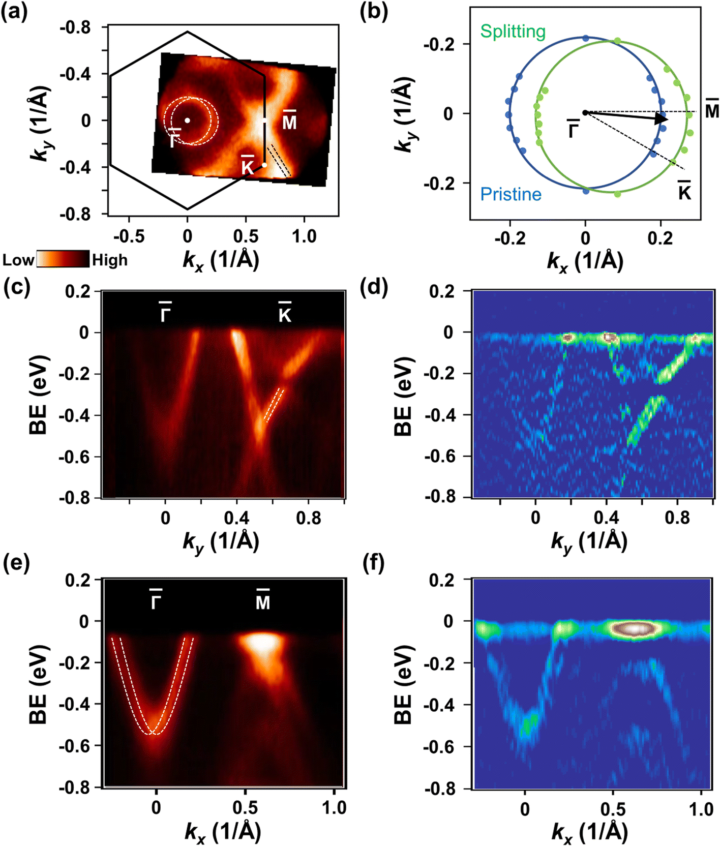 | ||
| Fig. 2 Fermi surface (FS) topology and band dispersion of Mn-doped CVS. (a) FS mapping performed at 80 K with 21.2 eV photons. (b) FS-fitted curves of the Γ-center pocket, showing that the FS is broadened at the Γ point and the electron pocket of the original degenerate states splits into two rings. The splitting scale is ∼0.06 Å−1. Band dispersions along the Γ–K (c) and Γ–M (e) directions. (d and f) Second derivative of the energy distribution curves in (c) and (e), respectively. The white dashed lines represented the energy band splitting mode, showing that splitting appeared along both the Γ–K and Γ–M directions, with different splitting scales. | ||
We would like to discuss the origin of such band splitting. Firstly, we can rule out the lattice symmetry breaking effect, because the direction of the largest splitting scale is slightly away from the Γ–M direction with an angle of ∼10°. Secondly, it also can't be due to the temperature-related phase transition, because the energy band splitting can persist up to room temperature, as shown in Fig. S4,† well above the CDW transition temperature. The splitting features in our samples were different from those of the band reconstruction induced by temperature evolution38 or two-fold lattices caused by symmetry breaking27 in the CVS system. Thirdly, the band splitting also could not be due to long-range magnetic order. Our temperature-dependent magnetization (M–T) measurements show that there is no long-range magnetic order peak observed above 80 K. In the field-cooled (FC) measurement (as shown in Fig. S5b†), the magnetization started to increase from ∼70 K and suddenly dropped near 50 K, and then a sharp peak appeared. Similar magnetic peaks have been observed in the weak interlayer antiferromagnetic coupling in MnBi2Te4,39 MnBi4Te7 (ref. 40) and CoNb3S6.41 In these materials, weak antiferromagnetic (AFM) coupling dominates and interlayer ferromagnetic (FM) exchange decreases with increasing interlayer spacing. This image of long-range magnetic moment interactions resembles the sparse distribution of Mn in the CVS lattice. Moreover, weak AFM coupling hysteresis loops are usually found in the high field range. Our field-dependent magnetization (M–H) measurements also show a small hysteresis loop in the range of 3–6 T, indicating a very weak AFM coupling in the Mn sample (see Fig. S5a†). It is implied that a weak paramagnetic (PM) to AFM transition may exist in the Mn samples near 50 K. Thus, the low concentration of Mn atoms only provides a local magnetic moment with a weak antiferromagnetic order below 50 K, and no macroscopic magnetic field was established. Considering that the splitting scale is small and anisotropic, it is reasonable to believe that spin–orbit coupling (SOC) plays important roles in such band splitting. But it can't only be due to Rashba splitting, which would yield concentric circle structures. The lattice expansion along the c direction and locally inhomogeneous lattice distortion in Mn-doped CVS remind us of the Dresselhaus effect.42 Thus we ascribe such anisotropic double-ring band splitting to the combination of the Rashba effect and Dresselhaus effect.
3.3 Enhanced charge density wave after Mn doping
We found it difficult to directly measure the CDW gap near EF due to the local magnetism and lattice distortion induced by Mn doping, which will reduce the resolution of the electronic structure during ARPES measurements. We know that the CDW can break the symmetry of CVS and make the Dirac cone of the K point at ∼−0.3 eV open a large energy gap. The behaviour of this K point energy gap (named the Dirac cone gap here) is similar to that of the CDW gap, which can be used as a correlation feature to characterize CDW transition.43Fig. 3a and d exhibit the energy band dispersion and corresponding EDCs measured at 80 K in pristine CVS, which agree well with previous ARPES measurements.6 The electron band related to the Sb pz orbital (named the α band here) is clearly observed and results in a circular pocket at the Γ point. And one linear energy band (γ band) originated from the aV dxz/yz orbital forms a Dirac-cone-like dispersion structure between the Γ and K points. And the δ and ε bands were derived from the dxy/x2−y2 orbital and intersected forming multiple Dirac points at the K point.14,29 We can identify a large energy gap (Dirac cone gap) at such a Dirac cone, which is much clearer from EDCs shown in Fig. 3d. We have conducted the temperature evolution measurement, as shown in Fig. S7.† | ||
| Fig. 3 Dirac cone gap at the K point of pristine CVS and Mn-doped CVS. (a and d) Energy band dispersion and the corresponding energy distribution curves (EDCs) measured at 80 K in pristine CVS. (b and c) ARPES intensity along the Γ–K direction measured at T = 80 K and 140 K, respectively. (e and f) Corresponding EDCs of (b) and (c), respectively. Blue triangles are guides for the eye to mark the peak positions of EDCs. (g) Temperature evolution of the Dirac cone gap is performed from 80 K to 140 K at a 10 K interval. Orange triangles indicate the peak position of EDCs, expressing the size of the Dirac cone gap. (h) The Dirac cone gap size was extracted and fitted. The Dirac cone gap decreased with temperature and nearly disappeared at 135 K ± 5 K. | ||
These bands were also found in Mn-doped CVS, but with band splitting. Fig. 3b and c show the ARPES intensity of Mn-doped CVS along the Γ–K direction measured at a temperature of 80 K and 140 K, respectively. The corresponding EDCs are shown in Fig. 3e and f, respectively. The temperature evolution measurement of such a CDW-related gap was performed from 80 K to 140 K at a 10 K interval (see more data in Fig. S6 in the ESI†). It was found that the Dirac cone gap decreases with temperature and disappeared at 135 K ± 5 K, as demonstrated in Fig. 3g and h. In the pristine sample, the Dirac cone gap disappeared at ∼95 K (see Fig. S7†), same as the CDW transition temperature of 94 K, indicating a correlation feature between the Dirac cone gap and CDW gap. We also carried out electronic transport and magnetic susceptibility measurements (see Fig. S8†) on Mn-implanted CVS samples, and observed an additional resistance kink at ∼150 K in both the R–T curve and M–T curve, which agrees quite well with the ARPES results, indicating enhanced CDW transition. In other words, the CDW transition in Mn-doped CVS is significantly enhanced to 135 K by Mn ion implantation, which is much different from the reported cases of charge doping via chemical substitution.44–46 We also carried out doping dependent ARPES experiments (see Fig. S9†) and found that the gap size and closing temperature of the Dirac cone gap at the K point increase with the Mn doping level, which demonstrates a close correlation between Mn implantation and the enhanced CDW transition.
3.4 The mechanism of enhanced CDW modulation
After establishing the enhanced CDW modulation after implanting Mn atoms, we would like to discuss the mechanism. We can rule out the charge doping effect, because there was no Fermi level shift or Fermi surface topology change from ARPES measurements. The small amount of charge released by the Mn atom provides only an additional local spin magnetic moment and has rare carrier contribution to CVS. We found that a mist trailing below the conduction band near the Γ point appears in pristine CVS, as shown in Fig. 4a, which could not be classified as temperature-dependent band splitting or a kind of surface-induced orbital-selective band reconstruction.47 Remarkably, such trailing electronic states were suppressed in Mn-doped CVS, as shown in Fig. 4b. Instead, we observed clear spectral weight transfer from the conduction band to the energy level near the EF. More details are available in Fig. S8 in the ESI.† We also plot the EDCs along the Γ–K direction in pristine and Mn-doped CVS with different doping levels in Fig. 4c. By increasing the doping level, the relative spectral weight close to EF was enhanced significantly. In samples with the highest doping, the spectral weight of conduction band electrons at the Γ point is even higher than that of valence band electrons. We found that the transfer is from the low energy level to the high energy level, similar to the excitation of electronic states and also consistent with the suppression of the trailing states. The trailing structure may consist of a series of small energy levels and originate from a plasma radical polarizer, which is generated by the strong coupling of holes and plasma excitons in pristine CVS. In addition, the excitation process is also similar to the exciton-insulator excitation in 1T-TiSe2 and Ta2NiSe5.48–51 Such a kind of excitation state implies that the Coulomb shielding of electron–hole pairs becomes weaker in Mn-doped samples, which decreases the carrier concentration. | ||
| Fig. 4 ARPES intensity near the Γ point measured at 80 K. (a) Comparison of the ARPES intensity around the Γ point of pristine and Mn-doped CVS samples. The intensity peaks extracted from EDCs were marked with white dashed lines. (b) Corresponding MDC curves of (a). A mist trailing below the conduction band is more clearly observed in pristine CVS, and the trailing electronic states were suppressed in doped CVS. (c) The EDCs for different doping concentrations at T = 80 K, showing the spectral weight of the conduction band transferring to an energy level near the EF. (d) Temperature evolution of the EDC and Kondo resonant peaks labelled η1 (green triangles) and η2 (yellow triangles). Peak η2 appeared at −0.2 eV, and vanished when the temperature increased to 210 K. | ||
The decreased carrier concentration is also evidenced by temperature-dependent experiments. As shown in Fig. 4d, the two peaks of η1 and η2 can be identified in the EDC around the Γ point. Peak η2 appears at 0.2 eV below EF and vanishes when the temperature goes to 210 K. Such evolution reminds us of the situation of d-orbital Kondo resonance peaks appearing in Fe3GeTe2 and FeTe.52,53 Considering the implanted magnetic Mn atoms and weak AFM transition at low temperature, the η1 and η2 peaks should be the Kondo resonant peaks. The related ARPES intensity map and second derivative are presented in Fig. S10.† And the EDC divided by temperature-dependent Fermi–Dirac distribution is displayed in Fig. S11.† Due to the enhancement of the spectral weight near EF caused by plasmon excitation states, the spectral weight for the Kondo peak near EF was hard to distinguish. Fortunately, the η2 exhibits a typical resonant peak behaviour. In a word, the Kondo shielding effect on the conducting electrons together with trail spectral weight transfer for plasmon polaron excitation decreases the carrier concentration. More microscopic experimental evidence and theoretical analysis are needed to further reveal the relations between the Kondo effect and CDW in Mn-doped CVS.
4 Conclusions
In summary, we successfully implanted magnetic Mn atoms into the CsV3Sb5 bulk via a well-designed method. By using high-resolution ARPES, we observed an anisotropic band splitting slightly away from Γ–M direction, which was ascribed to the combined effect of Rashba and Dresselhaus. Furthermore, enhanced CDW transition was identified in Mn-doped CVS, which should be due to the decreased charge concentration, according to the observed polariton excitation and Kondo shielding effect. Our study here not only provides an innovative idea to modulate the rich physical phenomena such as charge order, symmetry and topology in the CVS system, but also shows the advantages of ion implantation doping to tune electronic structures.Author contributions
F. L. supervised the project. X. L. and P. W. designed and performed the ion implantation and ARPES experiments with the help of A. C., L. C., T. W. and Y. C. Y. Z. performed the STEM measurements. M. M. and Y. W. carried out the magnetic measurements. R. H. performed the TOF-SIMS measurements. The manuscript was written through the contributions of all authors, and all authors have approved the final version of the manuscript.Conflicts of interest
There are no conflicts to declare.Acknowledgements
This work was supported by the National Natural Science Foundation of China (Grant No. 11634007 and 92065206), the Suzhou Science and Technology Program (Grant No. SJC2021009) and the Natural Science Foundation of Shandong Province (Grant No. ZR2020MA071). The support from the Vacuum Interconnected Nanotech Workstation (Nano-X) of the Suzhou Institute of Nanotech and Nano-bionics, Chinese Academy of Sciences is also acknowledged.References
- B. R. Ortiz, L. C. Gomes, J. R. Morey, M. Winiarski, M. Bordelon, J. S. Mangum, I. W. H. Oswald, J. A. Rodriguez-Rivera, J. R. Neilson, S. D. Wilson, E. Ertekin, T. M. McQueen and E. S. Toberer, Phys. Rev. Mater., 2019, 3, 094407 CrossRef CAS.
- X. L. Feng, K. Jiang, Z. Q. Wang and J. P. Hu, Sci. Bull., 2021, 66, 1384–1388 CrossRef CAS PubMed.
- H. X. Li, T. T. Zhang, Y. Y. Pai, C. Marvinney, A. Said, T. Yilmaz, Q. Yin, C. Gong, Z. Tu, E. Vescovo, R. G. Moore, S. Murakami, H. C. Lei, H. N. Lee, B. Lawrie and H. Miao, Phys. Rev. X, 2021, 11, 031050 CAS.
- X. X. Wu, T. Schwemmer, T. Müller, A. Consiglio, G. Sangiovanni, D. Di Sante, Y. Iqbal, W. Hanke, A. P. Schnyder, M. M. Denner, M. H. Fischer, T. Neupert and R. Thomale, Phys. Rev. Lett., 2021, 127, 177001 CrossRef CAS PubMed.
- C. C. Zhu, X. F. Yang, W. Xia, Q. W. Yin, L. S. Wang, C. C. Zhao, D. Z. Dai, C. P. Tu, B. Q. Song, Z. C. Tao, Z. J. Tu, C. S. Gong, H. C. Lei, Y. F. Guo and S. Y. Li, Phys. Rev. B, 2022, 105, 094507 CrossRef CAS.
- B. R. Ortiz, S. M. L. Teicher, Y. Hu, J. L. Zuo, P. M. Sarte, E. C. Schueller, A. M. M. Abeykoon, M. J. Krogstad, S. Rosenkranz, R. Osborn, R. Seshadri, L. Balents, J. F. He and S. D. Wilson, Phys. Rev. Lett., 2020, 125, 247002 CrossRef CAS PubMed.
- B. R. Ortiz, P. M. Sarte, E. M. Kenney, M. J. Graf, S. M. L. Teicher, R. Seshadri and S. D. Wilson, Phys. Rev. Mater., 2021, 5, 034801 CrossRef CAS.
- Z. Liang, X. Hou, F. Zhang, W. Ma, P. Wu, Z. Zhang, F. Yu, J. J. Ying, K. Jiang, L. Shan, Z. Y. Wang and X. H. Chen, Phys. Rev. X, 2021, 11, 031026 CAS.
- S. L. Ni, S. Ma, Y. H. Zhang, J. Yuan, H. T. Yang, Z. Y. W. Lu, N. N. Wang, J. P. Sun, Z. Zhao, D. Li, S. B. Liu, H. Zhang, H. Chen, K. Jin, J. G. Cheng, L. Yu, F. Zhou, X. L. Dong, J. P. Hu, H. J. Gao and Z. X. Zhao, Chin. Phys. Lett., 2021, 38, 057403 CrossRef CAS.
- J. F. Zhang, K. Liu and Z. Y. Lu, Phys. Rev. B, 2021, 104, 195130 CrossRef CAS.
- R. Lou, A. Fedorov, Q. Yin, A. Kuibarov, Z. Tu, C. Gong, E. F. Schwier, B. Buechner, H. Lei and S. Borisenko, Phys. Rev. Lett., 2022, 128, 036402 CrossRef CAS PubMed.
- M. Y. Jeong, H. J. Yang, H. S. Kim, Y. B. Kim, S. Lee and M. J. Han, Phys. Rev. B, 2022, 105, 235145 CrossRef CAS.
- M. G. Kang, S. Fang, J. K. Kim, B. R. Ortiz, S. H. Ryu, J. Kim, J. Yoo, G. Sangiovanni, D. Di Sante, B. G. Park, C. Jozwiak, A. Bostwick, E. Rotenberg, E. Kaxiras, S. D. Wilson, J. H. Park and R. Comin, Nat. Phys., 2022, 18, 301–308 Search PubMed.
- Y. Hu, X. X. Wu, B. R. Ortiz, S. Ju, X. Han, J. Z. Ma, N. C. Plumb, M. Radovic, R. Thomale, S. D. Wilson, A. P. Schnyder and M. Shi, Nat. Commun., 2022, 13(1), 2220 Search PubMed.
- Q. Wang, P. F. Kong, W. J. Shi, C. Y. Pei, C. H. Wen, L. L. Gao, Y. Zhao, Q. W. Yin, Y. S. Wu, G. Li, H. C. Lei, J. Li, Y. L. Chen, S. C. Yan and Y. P. Qi, Adv. Mater., 2021, 33, 2102813 CrossRef CAS PubMed.
- T. Neupert, M. M. Denner, J. X. Yin, R. Thomale and M. Z. Hasan, Nat. Phys., 2022, 18, 137–143 Search PubMed.
- N. Shumiya, M. S. Hossain, J. X. Yin, Y. X. Jiang, B. R. Ortiz, H. Liu, Y. Shi, Q. Yin, H. Le, S. S. Zhan, G. Q. Chang, Q. Zhang, T. A. Cochran, D. Multer, M. Litskevich, Z. J. Cheng, X. P. Yang, Z. Guguchia, S. D. Wilson and M. Z. Hasan, Phys. Rev. B, 2021, 104, 035131 CrossRef CAS.
- H. Chen, H. Yang, B. Hu, Z. Zhao, J. Yuan, Y. Xing, G. Qian, Z. Huang, G. Li, Y. Ye, S. Ma, S. Ni, H. Zhang, Q. Yin, C. Gong, Z. Tu, H. Lei, H. Tan, S. Zhou, C. Shen, X. Dong, B. Yan, Z. Wang and H. J. Gao, Nature, 2021, 34587621 Search PubMed.
- F. H. Yu, D. H. Ma, W. Z. Zhuo, S. Q. Liu, X. K. Wen, B. Lei, J. J. Ying and X. H. Chen, Nat. Commun., 2021, 12, 3645 CrossRef CAS PubMed.
- C. Chan, Phys. Rev. B, 2016, 93, 184514 CrossRef.
- H. S. Xu, Y. J. Yan, R. Yin, W. Xia, S. J. Fang, Z. Y. Chen, Y. J. Li, W. Q. Yang, Y. F. Guo and D. L. Feng, Phys. Rev. Lett., 2021, 127, 187004 CrossRef CAS.
- L. P. Nie, K. L. Sun, W. R. Ma, D. W. Song, L. X. Zheng, Z. W. Liang, P. Wu, F. H. Yu, J. Li, M. Shan, D. Zhao, S. J. Li, B. L. Kang, Z. M. Wu, Y. B. Zhou, K. Liu, Z. J. Xiang, J. J. Ying, Z. Y. Wang, T. Wu and X. H. Chen, Nature, 2022, 604, 59–64 CrossRef CAS.
- B. Hu, Y. H. Ye, Z. H. Huang, X. Han, Z. Zhao, H. Yang, H. Chen and H. J. Gao, Chin. Phys. B, 2022, 31, 058102 CrossRef.
- K. Nakayama, Y. K. Li, T. Kato, M. Liu, Z. W. Wang, T. Takahashi, Y. G. Yao and T. Sato, Phys. Rev. B, 2021, 104, L161112 CrossRef CAS.
- H. Zhao, H. Li, B. R. Ortiz, S. M. L. Teicher, T. Park, M. Ye, Z. Wang, L. Balents, S. D. Wilson and I. Zeljkovic, Nature, 2021, 599, 216–221 CrossRef CAS PubMed.
- H. Li, H. Zhao, B. R. Ortiz, T. Park, M. Ye, L. Balents, Z. Q. Wang, S. D. Wilson and I. Zeljkovic, Nat. Phys., 2022, 18, 265–270 Search PubMed.
- Y. Xiang, Q. Li, Y. K. Li, W. Xie, H. Yang, Z. W. Wang, Y. G. Yao and H. H. Wen, Nat. Commun., 2021, 12, 301–308 Search PubMed.
- M. G. Kang, S. Fang, J. G. Yoo, B. R. Ortiz, Y. M. Oey, J. Choi, S. H. Ryu, J. Kim, C. Jozwiak, A. Bostwick, E. Rotenberg, E. Kaxiras, J. G. Checkelsky, S. D. Wilson, J. H. Park and R. Comin, Nat. Mater., 2023, 22, 186–193 CAS.
- K. Nakayama, Y. K. Li, T. Kato, M. Liu, Z. W. Wang, T. Takahashi, Y. G. Yao and T. Sato, Phys. Rev. X, 2022, 12, 011001 CAS.
- G. F. Ding, H. L. Wo, Y. Q. Gu, Y. M. Gu and J. Zhao, Phys. Rev. B, 2022, 106(23), 235151 CrossRef CAS.
- Y. P. Song, T. P. Ying, X. Chen, X. Han, Y. Huang, X. X. Wu, A. P. Schnyder, J. G. Guo and X. L. Chen, arXiv, 2021, preprint, arXiv:2105.09898, DOI:10.48550/arXiv.2105.09898.
- Y. M. Oey, B. R. Ortiz, F. Kaboudvand, J. Frassineti, E. Garcia, R. Cong, S. Sanna, V. F. Mitrovic, R. Seshadri and S. D. Wilson, Phys. Rev. Mater., 2022, 6, L041801 CrossRef CAS.
- H. T. Yang, Z. H. Huang, Y. H. Zhang, Z. Zhao, J. N. Shi, H. L. Luo, L. Zhao, G. J. Qian, H. X. Tan, B. Hu, K. Zhu, Z. Y. W. Lu, H. Zhang, J. P. Sun, J. G. Cheng, C. M. Shen, X. Lin, B. H. Yan, X. J. Zhou, Z. Q. Wang, S. J. Pennycook, H. Chen, X. L. Dong, W. Zhou and H. J. Gao, Sci. Bull., 2022, 67(21), 2176–2185 CrossRef CAS PubMed.
- Y. K. Li, Q. Li, X. W. Fan, J. J. Liu, Q. Feng, M. Liu, C. L. Wang, J. X. Yin, J. X. Duan, X. Li, Z. W. Wang, H. H. Wen and Y. G. Yao, Phys. Rev. B, 2022, 105, L180507 CrossRef CAS.
- M. Q. Liu, T. Han, X. R. Hu, Y. B. Tu, Z. Y. Zhang, M. S. Long, X. Y. Hou, Q. G. Mu and S. Lei, Phys. Rev. B, 2022, 106, L140501 CrossRef CAS.
- F. I. Allen, Beilstein J. Nanotechnol., 2021, 12, 633–664 CrossRef CAS PubMed.
- A. Das and D. Basak, ACS Appl. Electron. Mater., 2021, 3(9), 3693–3714 CrossRef CAS.
- Y. Luo, S. T. Peng, S. M. L. Teicher, L. W. Huai, Y. Hu, Y. Han, B. R. Ortiz, Z. W. Liang, Z. Y. Wei, J. C. Shen, Z. P. Ou, B. Q. Wang, Y. Miao, M. Y. Guo, M. Hashimoto, D. H. Lu, Z. H. Qiao, Z. Y. Wang, S. D. Wilson, X. H. Chen and J. F. He, Phys. Rev. B, 2022, 105, L241111 CrossRef CAS.
- J. F. Shao, Y. T. Liu, M. Zeng, J. Y. Li, X. F. Wu, X. M. Ma, F. Jin, R. Lu, Y. C. Sun, M. Q. Gu, K. D. Wang, W. B. Wu, L. S. Wu, C. Liu, Q. H. Liu and Y. Zhao, Nano Lett., 2021, 21(3), 5874–5880 CrossRef CAS PubMed.
- C. W. Hu, K. N. Gordon, P. F. Liu, J. Y. Liu, X. Q. Zhou, P. P. Hao, D. Narayan, E. Emmanouilidou, H. Y. Sun, Y. T. Liu, H. Brawer, A. P. Ramirez, L. Ding, H. B. Cao, Q. H. Liu, D. Dessau and N. Ni, Nat. Commun., 2020, 11(1), 97 CrossRef CAS.
- H. Tanaka, S. Okazaki, K. Kuroda, R. Noguchi, Y. Arai, S. Minami, S. Ideta, K. Tanaka, D. H. Lu, M. Hashimoto, V. Kandyba, M. Cattelan, A. Barinov, T. Muro, T. Sasagawa and T. Kondo, Phys. Rev. B, 2022, 105, L121102 CrossRef CAS.
- S. D. Ganichev and L. E. Golub, Phys. Status Solidi B, 2014, 251(9), 1801–1823 CrossRef CAS.
- Y. Hu, S. M. L. Teicher, B. R. Ortiz, Y. Luo, S. T. Peng, L. W. Huai, J. Z. Ma, N. C. Plumb, S. D. Wilson, J. F. He and M. Shi, Sci. Bull., 2022, 67, 495–500 CrossRef CAS.
- T. Kambe, S. Tsuboi, N. Nagao, Y. Nogami and K. Oshima, Phys. E, 2003, 18, 196–197 CrossRef CAS.
- A. Bussmann-Holder and A. R. Bishop, Phys. Rev. B: Condens. Matter Mater. Phys., 2009, 79, 0243032 Search PubMed.
- M. Kim, G. M. McNally, H. H. Kim, M. Oudah, A. S. Gibbs, P. Manuel, R. J. Green, R. Sutarto, T. Takayama, A. Yaresko, U. Wedig, M. Isobe, R. K. Kremer, D. A. Bonn, B. Keimer and H. Takagi, Nat. Mater., 2022, 21, 627–633 CrossRef CAS PubMed.
- L. W. Huai, Y. Luo, S. M. L. Teicher, B. R. Ortiz, K. Z. Wang, S. T. Peng, Z. Y. Wei, J. C. Shen, B. Q. Wang, Y. Miao, X. P. Sun, Z. P. Ou, S. D. Wilson and J. F. He, Chin. Phys. B, 2022, 31, 057403 CrossRef.
- Z. J. Lin, C. X. Wang, A. Balassis, J. P. Echeverry, A. S. Vasenko, V. M. Silkin, E. V. Chulkov, Y. G. Shi, J. D. Zhang, J. D. Guo and X. T. Zhu, Phys. Rev. Lett., 2022, 129, 187601 CrossRef CAS PubMed.
- A. Wegner, J. Zhao, J. Li, J. Yang, A. A. Anikin, G. Karapetrov, K. Esfarjani, D. Louca and U. Chatterjee, Phys. Rev. B, 2020, 101, 195145 CrossRef CAS.
- J. M. Bok, J. Hwang and H. Y. Choi, Phys. Rev. B, 2021, 103, 205108 CrossRef CAS.
- D. Werdehausen, T. Takayama, G. Albrecht, Y. F. Lu, H. Takagi and S. Kaiser, J. Phys.: Condens. Matter, 2018, 30, 305602 CrossRef PubMed.
- Y. Kim, M. Kim, M. S. Kim, C. M. Cheng, J. Choi, S. Jung, D. H. Lu, J. H. Kim, S. Cho, D. Song, D. Oh, Y. Li, Y. J. Choi, H. D. Kim, J. H. Han, Y. H. Jo, J. Seo, S. Huh and C. Kim, arXiv, 2022, preprint, arXiv:2203.06432, DOI:10.48550/arXiv.2203.06432.
- Y. Zhang, H. Y. Lu, X. G. Zhu, S. Y. Tan, W. Feng, Q. Liu, W. Zhang, Q. Y. Chen, Y. Liu, X. B. Luo, D. H. Xie, L. Z. Luo, Z. J. Zhang and X. C. Lai, Sci. Adv., 2018, 4, 6791 CrossRef PubMed.
Footnotes |
| † Electronic supplementary information (ESI) available. See DOI: https://doi.org/10.1039/d3na00216k |
| ‡ These authors contributed equally to this work. |
| This journal is © The Royal Society of Chemistry 2023 |