
 Open Access Article
 This Open Access Article is licensed under a Creative Commons Attribution-Non Commercial 3.0 Unported Licence
Absolute energy levels in nanodiamonds of different origins and surface chemistries†
Daria
Miliaieva
 *ae,
Aurelien Sokeng
Djoumessi
bc,
Jan
Čermák
a,
Kateřina
Kolářová
a,
Maximilian
Schaal
d,
Felix
Otto
d,
Ekaterina
Shagieva
a,
Olexandr
Romanyuk
a,
Jiří
Pangrác
a,
Jaroslav
Kuliček
e,
Vojtech
Nádaždy
fg,
Štěpán
Stehlík
ah,
Alexander
Kromka
a,
Harald
Hoppe
bc and
Bohuslav
Rezek
e
*ae,
Aurelien Sokeng
Djoumessi
bc,
Jan
Čermák
a,
Kateřina
Kolářová
a,
Maximilian
Schaal
d,
Felix
Otto
d,
Ekaterina
Shagieva
a,
Olexandr
Romanyuk
a,
Jiří
Pangrác
a,
Jaroslav
Kuliček
e,
Vojtech
Nádaždy
fg,
Štěpán
Stehlík
ah,
Alexander
Kromka
a,
Harald
Hoppe
bc and
Bohuslav
Rezek
e
aInstitute of Physics, Czech Academy of Sciences, Na Slovance 1999/2, 182 21 Prague 8, Czech Republic. E-mail: miliaieva@fzu.cz
bCenter for Energy and Environmental Chemistry Jena (CEEC Jena), Friedrich Schiller University Jena, Philosophenweg 7a, 07743 Jena, Germany
cLaboratory of Organic and Macromolecular Chemistry (IOMC), Friedrich Schiller University Jena, Humboldstrasse 10, 07743 Jena, Germany
dInstitute of Solid State Physics, Friedrich Schiller University Jena, Helmholtzweg 5, 07743 Jena, Germany
eFaculty of Electrical Engineering, Czech Technical University in Prague, 166 27 Prague, Czech Republic
fInstitute of Physics, Slovak Academy of Sciences, Dúbravská cesta 9, 845 11 Bratislava, Slovak Republic
gCentre for Advanced Material Application, Slovak Academy of Sciences, Dúbravská cesta 9, 845 11 Bratislava, Slovak Republic
hNew Technologies – Research Centre, University of West Bohemia, Univerzitní 8, 306 14, Pilsen, Czech Republic
First published on 20th June 2023
Abstract
Nanodiamonds (NDs) are versatile, broadly available nanomaterials with a set of features highly attractive for applications from biology over energy harvesting to quantum technologies. Via synthesis and surface chemistry, NDs can be tuned from the sub-micron to the single-digit size, from conductive to insulating, from hydrophobic to hydrophilic, and from positively to negatively charged surface by simple annealing processes. Such ND diversity makes it difficult to understand and take advantage of their electronic properties. Here we present a systematic correlated study of structural and electronic properties of NDs with different origins and surface terminations. The absolute energy level diagrams are obtained by the combination of optical (UV-vis) and photoelectron (UPS) spectroscopies, Kelvin probe measurements, and energy-resolved electrochemical impedance spectroscopy (ER-EIS). The energy levels and density of states in the bandgap of NDs are correlated with the surface chemistry and structure characterized by FTIR and Raman spectroscopy. We show profound differences in energy band shifts (by up to 3 eV), Fermi level position (from p-type to n-type), electron affinity (from +0.5 eV to −2.2 eV), optical band gap (5.2 eV to 5.5 eV), band gap states (tail or mid-gap), and electrical conductivity depending on the high-pressure, high-temperature and detonation origin of NDs as well as on the effects of NDs' oxidation, hydrogenation, sp2/sp3 carbon phases and surface adsorbates. These data are fundamental for understanding and designing NDs' optoelectrochemical functional mechanisms in diverse application areas.
1 Introduction
Diamond nanoparticles, so-called nanodiamonds (NDs), are fascinating carbon-based nanomaterials, characterised by a rigid and stable diamond core and a reactive surface that can host multiple surface functional groups.1–5 The diamond lattice in the ND core keeps the bulk-like diamond structure down to a few nm,6 and allows the possibility to host stable colour centres such as nitrogen or silicon vacancies in sub-10 nm NDs.7–9 In contrast, due to the extremely high surface-to-volume ratio, it is the surface chemistry that controls NDs' colloidal and, in particular, electronic properties as well as interactions with other materials including biosystems.10–13 Oxidized and hydrogenated ND surfaces can be understood as two counterparts in terms of zeta potential sign as well as the remarkable difference in their work functions,14 and electrical conductivities.15 By analogy with experimental data on the negative electron affinity (NEA) of hydrogenated diamonds and the positive electron affinity (PEA) of oxidized diamonds,16–18 the calculations for NDs show that hydrogenated (and hydroxylated while in vacuum) NDs possess NEA,19,20 while oxidised NDs exhibit PEA.20 Moreover, NEA in nanodiamonds falls into two classes due to the lattice strain. The first class with a low NEA between −3.3 eV and −4.5 eV is strongly size-dependent. The second class with the higher NEA between 0 eV and −2.0 eV depends on ND anisotropy, but not on size.19Commercially available NDs often contain a non-diamond carbon phase (in the form of sp2 or amorphous carbon) that, for example, significantly impacts the catalytical21 or colloidal properties of NDs after hydrogenation.22 This set of unique chemical and structural properties as well as the great modification window makes NDs promising in various energy-oriented applications. For example, the successful application of NDs has been reported in photo-23,24 and electrocatalysis,25 supercapacitors,26 batteries27 and in optoelectronics as electron emitters,28 electrode substrates29 and materials for solar cell components.30,31
For understanding the roles of NDs and the effects they may have on the optoelectronic applications, knowledge about their energy band structure is essential. Usually, energy levels of nanodiamonds are approximated by the energy levels of the bulk diamond24,32 which may not be easily applicable due to the above-mentioned large variability in the ND material properties, namely the size, structure, and surface chemical properties. So far, only partial data and sometimes inconsistent data have been reported. In particular, only relative energy level shifts have been shown in NDs with oxidized and hydrogenated surface chemistry14,33 and inconsistent values of ND electronic bandgaps were reported.30,34 Also, support by theoretical approaches is limited to very small ND models due to the enormous computational cost of the larger ND particles. Here, by means of density functional theory (DFT) calculations, the energy diagrams for sub-1 nm NDs of different surface chemistries were constructed.35 However, the direct applicability of the data obtained for such small NDs is questionable due to the inherent quantum confinement at this scale.36
This work presents the comprehensive opto-electronic-chemical study of the as-received, fully hydrogenated (reduced) and fully oxidized NDs. Certain variation of the ND structure is ensured by the employment of monocrystalline high-pressure high-temperature (HPHT) and “polycrystalline” and defective detonation NDs (DNDs). UV-visible, ultraviolet photoemission, and electrochemical impedance spectroscopies are combined with the Kelvin probe and the absolute values of the energy levels for NDs are presented and elaborated by the electronic density of states. The profound effect of the non-diamond phase in NDs of particular surface chemistries is discussed. Finally, the model comprising the combined effect of the surface chemistry and the carbon hybridisation on the energy levels is suggested which opens the way for predicting the ND behaviour in the prospective applications and explains the ND function mechanism in the reported optoelectronic applications.
2 Experimental part
2.1 Materials
Nanodiamonds of different origins and surface chemistries were the subjects of this study. NDs of detonation origin (DNDs) were purchased from New Metals and Chemicals Corp., Japan (purity >98%). The mean size of the primary DND particles is ∼5 nm. This sample in the as-received state is further denoted as DND-ar. Monocrystalline high-pressure high-temperature (HPHT) NDs were purchased from Pureon, Switzerland. The size range is 0–30 nm and the mean size is ∼18 nm, the least of the commercially available sizes for HPHT NDs. This sample in the as-received state is further labelled as HPHT ND-ar.The surface annealing of NDs was performed with the optimal parameters to assure the fullest hydrogenation/oxidation keeping a similar size distribution to the as-received ND material37 (Fig. S1†). To prepare oxidized DNDs, air annealing at 450 °C for 30 min was performed which leads to surface oxidation and purification;38 longer annealing and/or higher temperature already leads to unwanted etching of the DNDs.39,40 Due to an average larger size and monocrystalline structure, HPHT NDs can be nearly completely purified from the sp2-C at 450 °C for 300 min.41 This is the well-established and widely used (i.e. relevant) annealing procedure in the air that has been proven many times for cleaning and oxidation of the nanodiamond surface42 and introduction of the carboxylic groups or their corresponding dehydrated forms—anhydrides on the ND surface.43 The oxidized DNDs are denoted as DND-O and oxidized HPHT NDs as HPHT ND-O.
Hydrogenation of DNDs is already a well-established process.44 It was shown that for complete hydrogenation of DNDs in hydrogen gas, a temperature of 600 °C is sufficient.45–47 However, to fully hydrogenate HPHT NDs, a significantly higher temperature of 750–800 °C is needed as shown recently.48–50 Thus, to hydrogenate the ND surface DND-ar and HPHT ND-O were annealed in hydrogen gas (flow rate was 5 l min−1) for 6 h at atmospheric pressure at 700 °C for DNDs and 800 °C for HPHT ND.48 The hydrogenated samples are labelled as DND-H and HPHT ND-H.
2.2 Preparation of ND samples for characterization
Each ND stock colloid was prepared by sonicating 1 mg of a particular ND powder in 1 ml of deionized water in a 2 ml polypropylene test tube using a sonication horn for 1 h at 100 W (Hielscher UP 200s sonicator and S2 titanium sonotrode) in 0.5 s on/off regime. Cooling was ensured by immersing the test tube in a 1 l container filled with cold water. Such prepared colloids were used for DLS measurements and 100 times diluted (to reach 0.01 mg ml−1 concentration) for UV-visible spectroscopy measurements. The uniform layers were deposited by spin-coating colloids at 1500 rpm on gold-coated silicon substrates for KP, UPS, and XPS and ITO for ER-EIS measurements. For measurements of work functions of NDs by KP without adsorbates, the samples were annealed in a glove box in a nitrogen atmosphere for 1 h at 250 °C (ref. 14) and then kept in the glove box during all the measurements.To study the scattering contribution we fractionated the DND-ar stock colloid (Fig. S2†). We extracted a transparent fraction with a DND-ar size range of 10–70 nm by centrifuging (Eppendorf Mini plus) the stock colloid at 14![[thin space (1/6-em)]](https://www.rsc.org/images/entities/char_2009.gif) 500 rpm for 1 h, after which 0.8 ml of the supernatant was isolated and characterised by DLS and UV-vis (previously diluted to 0.01 mg ml−1). The fraction with 70–700 nm of DND-ar, which caused turbidity of the DND-ar colloid, was obtained by decanting the stock colloid overnight. Then the supernatant was centrifuged at 14500 rpm for 3 min. The sediment was isolated and sonicated in 2 ml of water for 10 min using a sonotrode and characterised by DLS and UV-vis (previously diluted to 0.01 mg ml−1).
500 rpm for 1 h, after which 0.8 ml of the supernatant was isolated and characterised by DLS and UV-vis (previously diluted to 0.01 mg ml−1). The fraction with 70–700 nm of DND-ar, which caused turbidity of the DND-ar colloid, was obtained by decanting the stock colloid overnight. Then the supernatant was centrifuged at 14500 rpm for 3 min. The sediment was isolated and sonicated in 2 ml of water for 10 min using a sonotrode and characterised by DLS and UV-vis (previously diluted to 0.01 mg ml−1).
2.3 Experimental techniques
The equation (αhν)2 = A(hν − Eg), formulated by Tauc51 and elaborated by Davis and Mott,52 introduces the coordinates (αhν)2 − hν for the determination of the bandgap (Eg) of the amorphous semiconductors (in NDs the crystallinity of the diamond-like core is typically combined with a non-diamond phase which makes the Tauc theory applicable to NDs). The steep linear part of the plot intercepts with the background line of the plot at the point at which (and below) the absorption coefficient is equal to zero, thus, at the value of a bandgap. The uncertainty of bandgap estimation is equal to the sum of uncertainties of the wavelength measurement and linear fit.
Absorption coefficient α is calculated from the Lambert–Beer Law, according to which both absorption and scattering might contribute to the absorbance. The scattering plays a significant role only in DNDs due to the presence of 70–700 nm agglomerate fraction (Fig. S2†) and will be taken into account while determining the Eg of DNDs. Knowing the I0 and I – the intensities of incoming and outcoming light in the cuvette; d – cuvette side length or the light path length in cm (in our case it was 1 cm); A – absorbance (a.u.),
| I0 = e−αd | (1) |
| log(I0) = A | (2) |
The work function was determined by (i) fitting a linear function to the slope of the low-energy secondary electron cut-off (SECO) and measuring the intercept with the constant background and (ii) subtracting this cut-off energy from the excitation energy. A bias of ≈−9 eV was applied to the sample for measuring the SECO and then subtracted from the kinetic energy results. The bias voltage is needed to measure photoelectrons with low kinetic energy since the setup allows the detection of electrons with kinetic energy higher than 5 eV. At very low kinetic energies, the collection and focusing of the photoelectrons on the entrance slit of the hemispherical electron energy analyzer by the electromagnetic lens do not work properly. For a constant electric field to accelerate the photoelectrons and increase their kinetic energy, we need to use a constant voltage source with a bias voltage (the amount of the bias voltage in V corresponds to the change of the kinetic energy in eV). The latter should be high enough to allow measuring samples with a very low work function.
The onset of the valence band was determined by fitting a linear function to the slope of the UPS signal (in the lower energy range of the binding energy coordinates) and measuring the intercept with the constant background. This intercept represents the difference |EF − EV|. With the known absolute position of the Fermi level (binding energy of 0 eV) and the work function, the position of the valence band relative to the vacuum level was recalculated.53
UPS technique is also successfully used to disclose the DOS at the valence band. The disadvantage of the technique in nanodiamond study is the risk of possible surface modification (graphitisation and/or desorption surface functional groups) at UV energies. Therefore, a non-contact and non-spectroscopic method like the Kelvin probe might be advantageous for the work function determination of nanodiamonds.
KP measurements were done in a dry nitrogen-filled glove box using a grounded steel probe tip of 2 mm diameter and scanning the sample at 250 points. As the reference, a polished Si sample with thermally evaporated 10 nm of Ti and 150 nm of Au on the top was used.
3 Results and discussion
3.1 Surface chemistry and structure of NDs
Before addressing the optoelectronic properties, it is important to highlight structural and chemical differences among the ND samples.
Fig. 1 shows SEM images of HPHT ND-ar (a) and DND-ar (b) which are representative of the HPHT and DND samples, respectively, independent of the surface chemistry. HPHT NDs have a highly irregular shape; still, the distinct faceting of the nanocrystals is noticeable. DNDs' contours are already blurred due to their significantly smaller size. Numerous previous TEM studies showed that the shape of the DND primary particles is roundish with a certain degree of faceting.56 FTIR and Raman spectroscopies are excellent tools to reveal and describe the important differences in the surface chemistry and structure of the HPHT ND and DND samples. FTIR spectroscopy is a well-established and convenient technique to analyse the ND surface chemistry. Interestingly, recent reports reveal that it can also be applied to investigate electrical conductivity in hydrogenated NDs.57,58 The FTIR spectra of HPHT ND (Fig. 1c) and DND (Fig. 1d) samples clearly revealed different surface chemistries of the as-received materials, HPHT ND-ar and DND-ar (grey curves), which is obviously due to the different purification treatments performed by the particular manufacturer. HPHT ND-ar sample is characterised by oxygen-rich surface functional groups such as the C![[double bond, length as m-dash]](https://www.rsc.org/images/entities/char_e001.gif) O group (1700–1800 cm−1) and OH groups coming from surface C–OH bonds59 and/or surface adsorbed water60 (3000–3700 cm−1 OH stretching and ∼1630 cm−1 OH bending). DND-ar is more polyfunctional, it contains both oxygen-rich moieties and hydrogen-rich moieties. The oxygen-rich moieties involve CO at 1720 cm−1, complex OH stretching at 3000–3700 cm−1 and bending at 1560–1670 cm−1. The sharp peak at 3700 cm−1 which also appears in the DND-H spectrum (Fig. 1d, blue) has been associated with the free, non-constrained by hydrogen bonds, OH stretching bonds of the adsorbed water.14 The hydrogen-rich moieties involve CHx (2800–3000 cm−1) stretching features. This complex surface chemistry gives this particular DND-ar sample quite specific properties.31,61 After air oxidation, the surface chemistry of both HPHT ND-O and DND-O became similar and characterised by a strong CO feature at 1800 cm−1 (ref. 62) attributed to carboxylic acid or its anhydride.63 Due to the negative zeta potential of oxidized NDs (between 30 mV and −40 mV) in deionised water (pH = 5) and the most pronounced FTIR feature at 1800 cm−1, we assume that the carboxylic group is chemically and electronically dominant on the ND-O surfaces.
O group (1700–1800 cm−1) and OH groups coming from surface C–OH bonds59 and/or surface adsorbed water60 (3000–3700 cm−1 OH stretching and ∼1630 cm−1 OH bending). DND-ar is more polyfunctional, it contains both oxygen-rich moieties and hydrogen-rich moieties. The oxygen-rich moieties involve CO at 1720 cm−1, complex OH stretching at 3000–3700 cm−1 and bending at 1560–1670 cm−1. The sharp peak at 3700 cm−1 which also appears in the DND-H spectrum (Fig. 1d, blue) has been associated with the free, non-constrained by hydrogen bonds, OH stretching bonds of the adsorbed water.14 The hydrogen-rich moieties involve CHx (2800–3000 cm−1) stretching features. This complex surface chemistry gives this particular DND-ar sample quite specific properties.31,61 After air oxidation, the surface chemistry of both HPHT ND-O and DND-O became similar and characterised by a strong CO feature at 1800 cm−1 (ref. 62) attributed to carboxylic acid or its anhydride.63 Due to the negative zeta potential of oxidized NDs (between 30 mV and −40 mV) in deionised water (pH = 5) and the most pronounced FTIR feature at 1800 cm−1, we assume that the carboxylic group is chemically and electronically dominant on the ND-O surfaces.
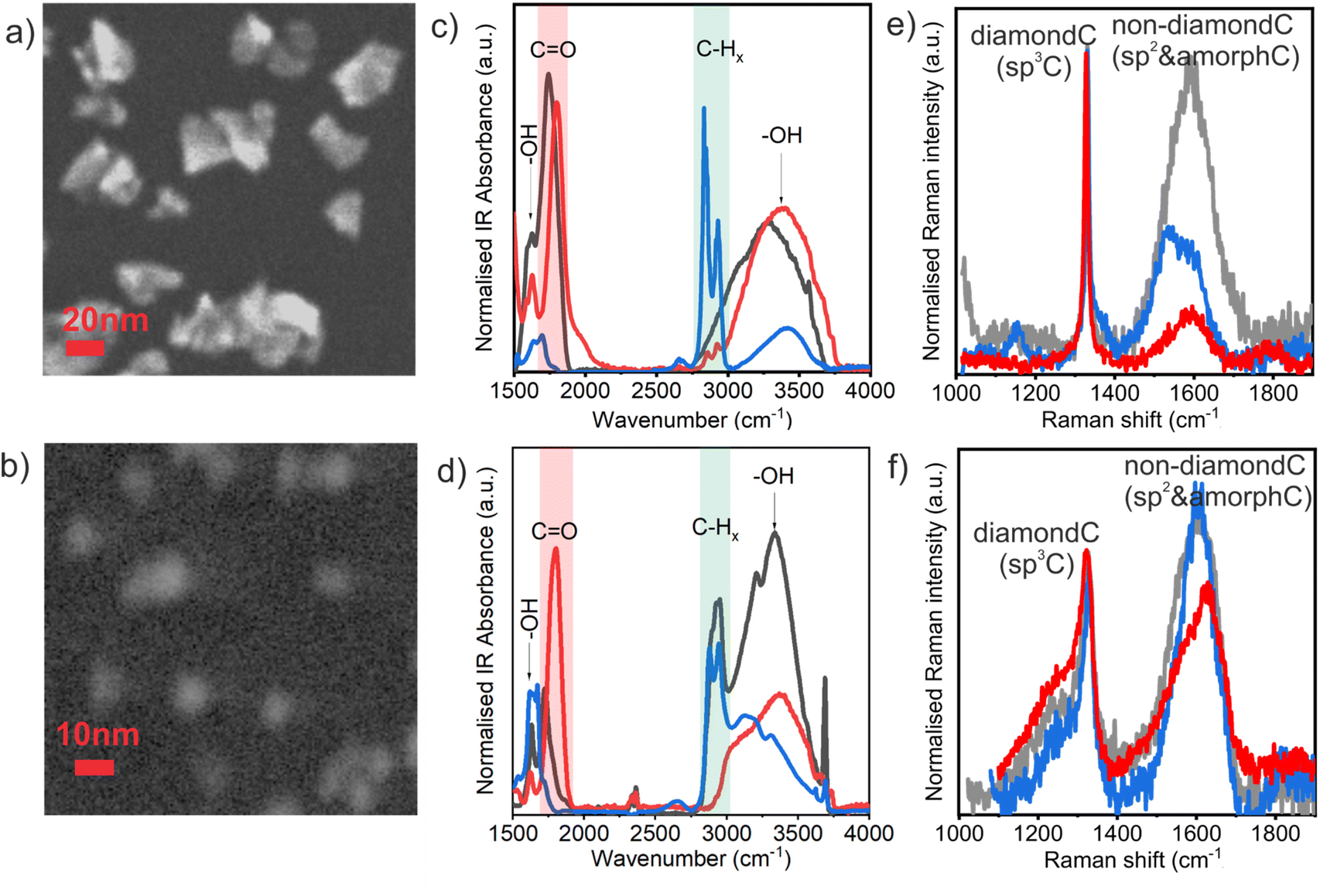 | ||
| Fig. 1 SEM images of the individual HPHT (a) and DND (b) particles. FTIR spectra of as-received (grey), oxidized (red) and hydrogenated (blue) HPHT (c) and DND (d). Raman spectra of as-received (grey), oxidized (red) and hydrogenated (blue) HPHT (e) and DND (f). | ||
In contrast, after hydrogenation, the oxygen-rich functional groups are greatly suppressed and the surface chemistry of DND-H and HPHT ND-H is dominated by –CHx bonds. Note that the greater OH bond contribution in DND-H compared to HPHT ND-H is possibly caused by stronger hydration of DND-H.48 It has been shown that DND-Hs bind the surface water very tightly even up to 250 °C.14,61
Raman spectroscopy further revealed important structural differences between the HPHT ND and DND samples (Fig. 1c and d), namely in the character of the non-diamond phase and the presence of defects in NDs. As highlighted in the recent studies,64 the DND Raman spectrum is characterised by a broadening and shift of the diamond Raman peak at 1332 cm−1 to lower wavenumbers as well as by the appearance of the low-frequency shoulder of the diamond peak due to the highly defective DND structure.39,40 This includes various point (vacancies, dangling bonds, substitutional nitrogen) and 2D defects (intercrystallite grain boundaries) which (i) decrease the effective coherent scattering domain well below the actual ND size that could be theoretically modelled by phonon confinement models65 and (ii) may induce heating from the excitation laser due to the increase of optical absorption.41 In monocrystalline HPHT NDs, no significant shifts of diamond Raman peak have been observed down to 2–3 nm.6,41
The part of Raman spectra above 1360 cm−1 is attributed to the non-diamond carbon and the exact position can be used for distinguishing between different non-diamond carbon forms.66 HPHT ND-ar has an intense non-diamond C band centred at 1590 cm−1 (indicative of graphitic carbon vibrations66) that stretches from the amorphous carbon region at ∼1520 cm−1 (ref. 66) to fragmented sp2 regions at 1640 cm−1.66 Such carbon disorder in HPHT ND-ar governs the electronic behaviour of HPHT ND-ar as will be shown further on. The highest graphitic content in HPHT ND-ar clearly correlates with the most intense dark tint of HPHT ND-ar colloidal solution (Fig. S1†). After annealing, the intensity of the non-diamond C band is greatly reduced and only a minor 1590 cm−1 component is present in HPHT ND-O (it remains in NDs even down to 5 nm or below) which is attributed to the extended structured sp2 nanocrystalline graphite-like regions.66
After hydrogenation, the peaks of the extended sp2 phase are present in HPHT ND-H, namely the nanocrystalline graphite peak at 1590 cm−1 and 1540 cm−1 peak which is assigned to the sp2 phase in which the bonds between carbon atoms are weakened.66 Interestingly, the Raman spectrum of the HPHT ND-H contains new features not present in any other NDs. The distinct feature of HPHT ND-H is the presence of trans-polyacetylene chains (TPA) which manifest in 1150 and 1450 cm−1 (merged in the wide G-band) peaks.66 The role of TPA in the optoelectronic properties will be discussed further on.
DNDs' non-diamond bands are centred in the ∼1600–1630 cm−1 range and correspond to fragmented sp2 regions and isolated sp2-bonded carbon atoms at the split interstitials.64 Already purified DNDs are seemingly less sensitive to oxidative thermal treatments compared to HPHT NDs due to the presence of non-diamond C not only on the surface but also in the volume.56,67 Thus, only a minor surface fraction of it is removed by annealing. Still, in the oxidized DND the sp2 C is possibly more fragmented (higher wavenumber) than in DND-ar and DND-H which is manifested by the shift of the non-diamond C band from 1600 to 1630 cm−1 after DND oxidation in air. The signal at ∼1640 cm−1 is sometimes attributed to OH vibrations. However, multiple studies showed that the contribution of the surface functional groups in the Raman spectra of DNDs is not significant.68,69 We also recently showed that the surface chemistry of oxidized DND and HPHT ND in a similar size range (around 5 nm or below) is similar. Yet, their Raman spectra are very different also in the 1620–1640 cm−1 spectral range.41 Thus, we suppose that the 1620–1640 cm−1 signal mostly comes from an isolated sp2-bonded carbon pair defect which occupies the position of one carbon atom in the normal diamond lattice as already suggested by Orwa et al.64
Thus, despite the similar surface chemistry the NDs of different origins differ in the carbon hybridisation and the nature of the defects which will be reflected in the optoelectronic properties.
3.2 Nanodiamonds' optical bandgaps
Complementary knowledge of ND structure and structural differences is essential for the interpretation of ND absorbance spectra measured by UV-vis spectroscopy. The raw absorption spectroscopy data are shown in Fig. S3.† For bandgap determination, the absorbance was recalculated to the absorption coefficient and further to the Tauc plots shown in Fig. 2.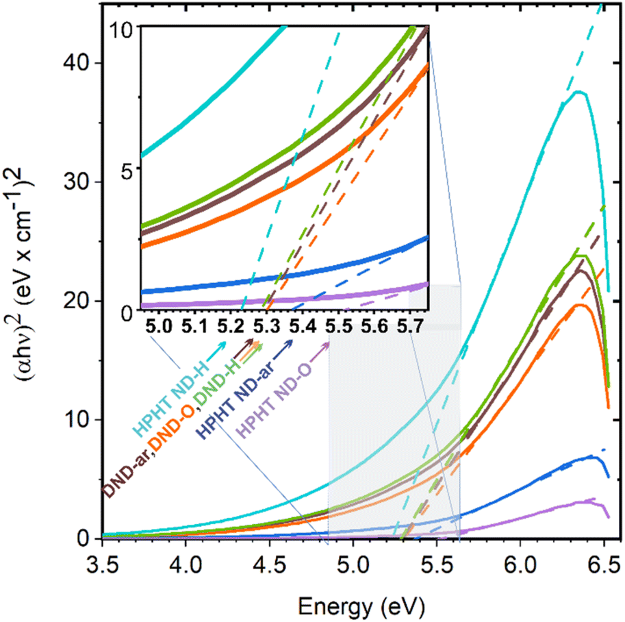 | ||
| Fig. 2 Tauc plots of the investigated ND samples. Absorption coefficient α was determined from UV-vis absorbance spectra. The inset's pointed values are NDs' bandgaps estimated from the intersections of the tangent to the Tauc plot and zero absorption coefficient line. | ||
The inset image shows the values of the bandgaps of NDs obtained at the point of intercept of the tangent to the Tauc plot and the zero-absorbance line.
Among all the ND samples, HPHT ND-O is characterised by the same optical bandgap value as the bulk diamond electronic bandgap, namely 5.480 ± 0.004 eV.32 Bandgap values of other HPHT ND samples are lower, namely 5.38 ± 0.01 eV for HPHT ND-ar and 5.21 ± 0.01 eV for HPHT ND-H. The deviation of HPHT ND-ar and HPHT ND-O bandgap value from the bulk diamond bandgap is caused by the non-diamond carbon content that introduces additional energy states into the electronic bandgap as was shown by DFT calculations20 leading to a decrease in the optical bandgap in NDs depending on the density of these intrabandgap states. Also, Nagata et al.30 observed the decrease of the bandgap in ND-ar using UV-vis spectrometry and explained it with the presence of the sp2+xC phase based on theoretical calculations.20
All the DND samples have similar optical bandgap values around ∼5.3 eV, independent of the surface chemistry and non-diamond C content, namely 5.30 ± 0.01 eV for DND-H; 5.31 ± 0.01 eV for DND-ar; and 5.31 ± 0.01 eV for DND-O. The formal deviation of DNDs' Eg from bulk diamond Eg is caused by scattering of the 70–700 nm fraction inherently present in DNDs. This fraction causes turbidity of the DND colloids (Fig. S2a†) and increases absorbance (Fig. S2b†) with an apparent bandgap of 5.1 eV (Fig. S2c†).
Since all the dominant size fractions of the used NDs (Fig. S1†) lie above the quantum confinement range which is assumed to appear below 2 nm in NDs,20 we do not suppose any influence of this effect on the obtained bandgap values.
Thus, for further consideration, we distinguish between the impact of (i) the diamond core sp3C, and (ii) non-diamond C content on the electronic properties of nanodiamonds. We assign to DNDs and HPHTs under consideration the electronic bandgap of 5.5 eV as if they were pure sp3C. By doing this we also subtract the effect of scattering on UV-vis measurement in the case of DNDs. The sp2 and amorphous carbon are taken into account via the incorporation of the additional states into the electronic bandgap of NDs as was done in the previous work of Reich.70
3.3 Nanodiamonds' valence band maxima (VBM) and the Fermi levels
To construct the NDs' energy diagram, the absolute position of the valence band maxima was determined by UPS (see Fig. 3). UPS spectra in the whole available range of the binding energies (BE) are shown in Fig. 3a. The lower BE energy range of UPS spectra (Fig. 3b) was used to determine the VBM position relative to the Fermi level (EF). Interestingly, the HPHT ND-H has filled energy states almost to the Fermi level and has the most pronounced photoemission among the other NDs.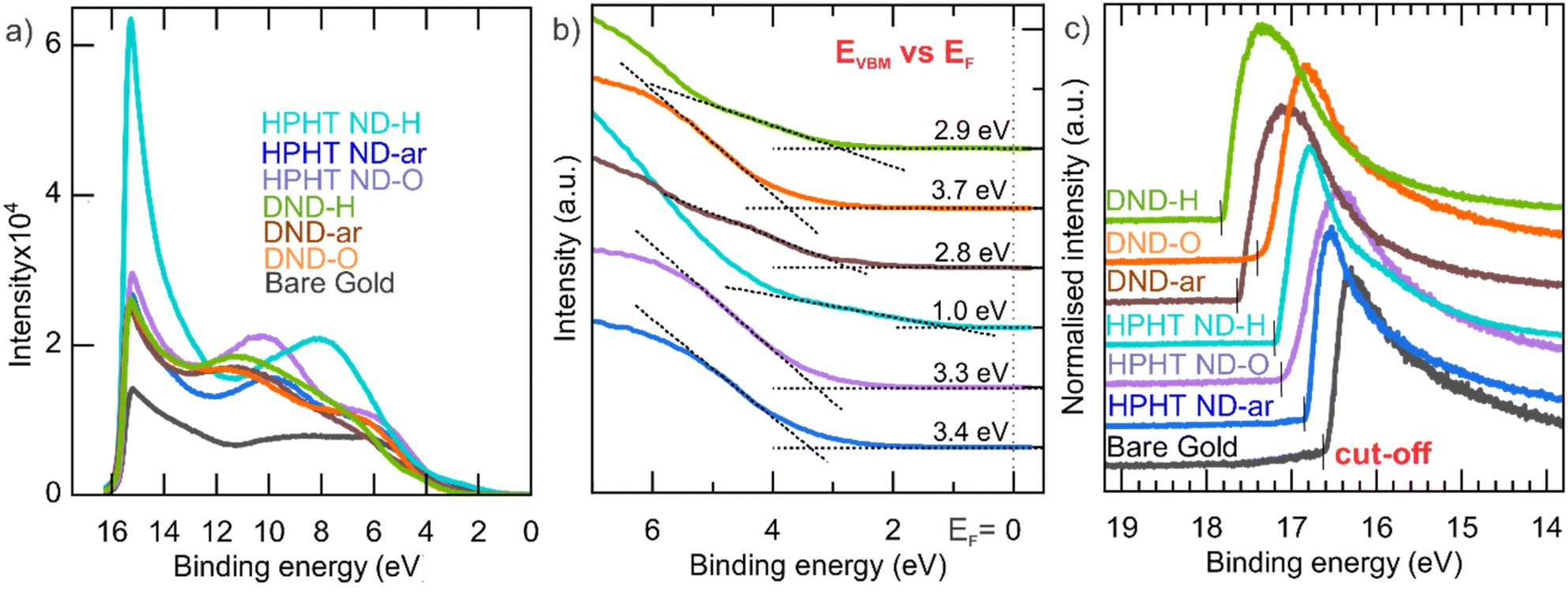 | ||
| Fig. 3 (a) UPS spectra in the whole energy range; (b) zoomed-in valence band onset region of UPS spectra relative to the EF; (c) zoomed-in cut-off energy region for determination of EFvs. vacuum. | ||
The higher BE (i.e., lower kinetic energies) range was used for the determination of the secondary electron cut-off (see Fig. 3c). All ND spectra have a distinct cut-off edge. Then, the Fermi energy level is calculated as EF (vs. vacuum) = Eexcitation − Ecut-off (Table 1). Clear shifts to higher work function values with surface oxidation happen in both HPHT NDs and DNDs.
| Material | E F vs. vacuum, eV | |EF − EVBM|, eV | E VBM vs. vacuum, eV |
|---|---|---|---|
| HPHT ND-H | −4.0 ± 0.1 | 1.0 ± 0.1 | −5.0 ± 0.1 |
| HPHT ND-ar | −4.4 ± 0.1 | 3.4 ± 0.1 | −7.8 ± 0.1 |
| HPHT ND-O | −4.2 ± 0.1 | 3.3 ± 0.1 | −7.5 ± 0.1 |
| DND-H | −3.4 ± 0.1 | 2.9 ± 0.1 | −6.3 ± 0.1 |
| DND-ar | −3.4 ± 0.1 | 2.8 ± 0.1 | −6.2 ± 0.1 |
| DND-O | −3.9 ± 0.1 | 3.7 ± 0.1 | −7.6 ± 0.1 |
Calculated values of the VBM position relative to the vacuum level are presented in Table 1. In general, VBM position highly depends on the ND surface chemistry, namely for the hydrogenated surface it lies in the range −5.0 to −6.3 eV below the vacuum level, while for the oxygenated surfaces, it lies in the range – 7.5–7.8 eV below the vacuum (Table 1).
The trend of the VBM downshift (vs. vacuum level) with the introduction of O-containing surface groups follows the trend already reported for carbon materials.33,71,73 Also, there is a downshift in VBM in HPHT ND-ar (−7.8 ± 0.1 eV) and DND-O (−7.6 ± 0.1 eV) compared to HPHT ND-O (−7.5 ± 0.1 eV). In the former materials, the non-diamond amorphous carbon phase content is higher than in the latter. Thus, the non-diamond amorphous carbon phase causes the downshift of VBM.
Interestingly, the HPHT ND-H valence band maximum is upshifted to −5.0 eV relative to the vacuum level. It lies in the range of VBMs of materials suitable for hole extraction at the heterojunction. This makes HPHT ND-H a prospective charge-transfer material in photovoltaics. Moreover, the ambient adsorbate O2/H2O with electrochemical level −5.3 eV (at ambient pH 6) vs. vacuum can p-dope the surface of HPHT ND-H with VBM at −5.0 eV, making the nanoparticle positively charged and possibly conductive as it was observed for hydrogenated microcrystalline diamond74 and bulk diamond.75 In general, any adsorbate with an electrochemical level below −5.0 eV supposedly p-dopes HPHT ND-H. The phenomenon of surface conductivity due to reversible electrochemical interaction between the semiconductor surface and its adsorbate which is enabled by the higher position of the valence band maximum of the semiconductor relative to the electrochemical level of the adsorbate is known as the surface transfer doping76,77 and was described first by Maier.78 P-doping due to high VBM can significantly contribute to the positive zeta potential of ND-H.22
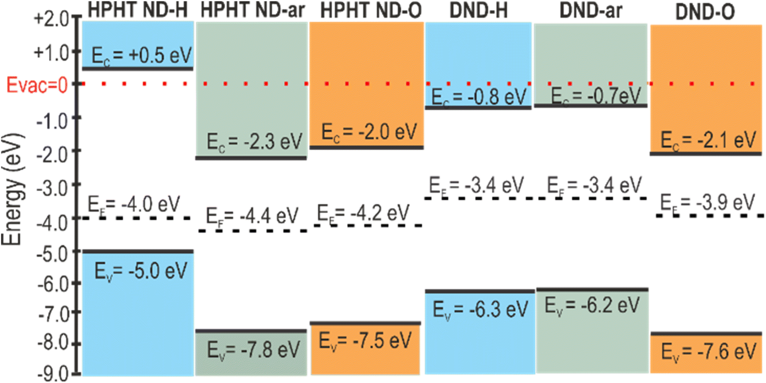
After compiling the results of UV-vis and UPS measurements, we constructed the energy level diagrams of HPHT ND and DND of as-received, hydrogenated, and oxidized surfaces (Scheme 1). On the vertical energy scale VBM, CBM (calculated as VBM + bandgap), and Fermi level are presented. The diagram clearly shows the downshift of VBM and Fermi level (vs. vacuum level) independently after oxidation and the presence of sp2 and amorphous carbon phases.
 | ||
| Scheme 1 Band diagrams of HPHT and DND nanodiamonds of as-received, hydrogenated, and oxidized surfaces. | ||
The diagram presents a striking difference in HPHT ND-H compared to other NDs, namely the high VBM of HPHT ND-H, which, combined with the bandgap value, locates the conduction band minimum (CBM) to +0.5 eV above vacuum. This results in the negative electron affinity (or NEA) of HPHT ND-H with important electrochemical consequences, such as the possibility of electron ejection into molecules such as water (CBM of water at ∼−0.8 eV below the vacuum level) and nitrogen (CBM at −0.2 eV below the vacuum level).79 The facilitation of electron ejection by HPHT ND-H compared to other NDs is also supported by XPS measurements (Fig. S4†). Interestingly, DND-Hs with the same surface chemistry as HPHT ND-H do not have the NEA most probably due to different non-diamond carbon forms in these materials that lead to different electronic properties. Other parameters such as size or shape do not significantly affect the presence or absence of NEA in this case. The specific crystallographic orientation of the hydrogenated diamond surface does influence the actual NEA value, but not its presence.80,81 Hydrogenated nanocrystalline diamond thin films with multifaceted and variously shaped nanoscale grains of different mean sizes, 80 and 250 nm, can be a good illustration for this since the NEA was present in all these films and allowed the operation of field-effect transistors.82 Effects such as a more defective structure and 2 at% of embedded N in DND-H may influence its conductivity and other electronic properties, but NEA is solely a property due to C–H bonds on the diamond surface.80,81 Therefore, we believe that the missing NEA on DND-H must be related to the non-diamond (namely, amorphous carbon) character of its surface despite the C–H bond termination of DND-H.
It should be notified that depending on the characterisation method and the presence of airborne adsorbates on the ND surfaces, work function values of the same ND sample might vary. Fig. 4a compares the work function obtained by the Kelvin probe (KP) and UPS. For HPHT NDs the work function values estimated by both techniques are similar. For DNDs, the work function by UPS appears to be systematically 0.7–0.9 eV lower compared to the work function obtained by KP. It could be due to the different responsiveness of DNDs to UV light compared to HPHTs. Also, the more pronounced curvature of DNDs compared to HPHT NDs could weaken the binding of π-electrons to the material leading to a decrease in the work function in UPS.73
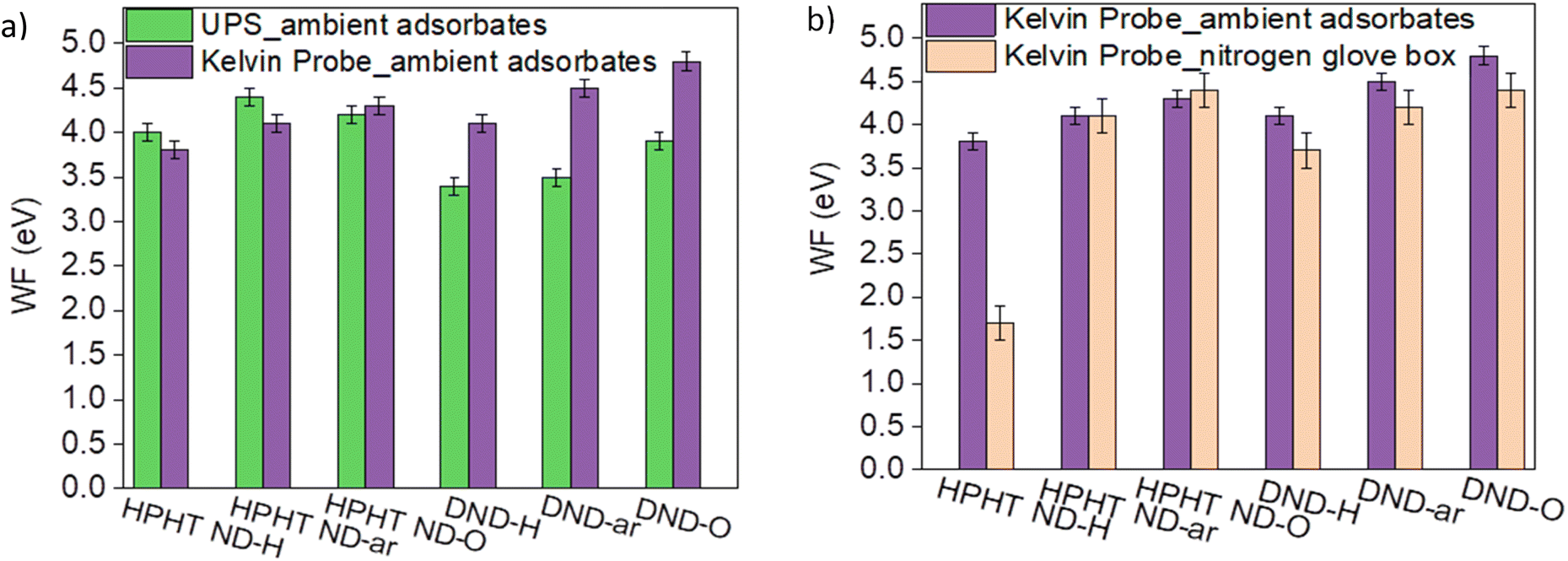 | ||
| Fig. 4 Comparison of WF work functions determined by (a) KP and UPS; (b) KP with and without ambient adsorbates. | ||
The trend of an increasing work function with increasing O content on the ND surface revealed by KP is consistent with the studies of the oxygenation impact on the work function in different materials72 and can be explained by the formation of CO dipoles which form the additional barrier for the electrons and thereby increasing the work function. The impact of the ambient adsorbates on NDs' work function Fig. 4b, namely O2/H2O, is very pronounced for HPHT ND-H. It confirms the electrochemical reaction between the high VBM of HPHT ND-H and the electrochemical level of the adsorbate species mentioned earlier. Such interactions can lead to an electron transfer from HPHT ND-H to O2/H2O, p-doping of ND and a subsequent downshift of the Fermi level with respect to the vacuum level equal to an increase of the work function that is clearly seen in Fig. 4b. The VBM position downshift relative to the Fermi level after heating was only about 0.3 eV compared to the VBM of the HPHT ND-H sample saturated with the ambient adsorbates (see Fig. S5†). The minor change of VBM in different environments could be explained by band bending due to the interaction of the HPHT ND-H surface with the adsorbates in the ambient.
3.4 The density of states (DOS) in nanodiamonds
The mapping of electronic states was performed with the ER-EIS technique, in which ER-EIS spectra directly reflect the DOS of ND layers. Fig. 5 shows the DOS spectra of the as-received, fully hydrogenated (reduced), and fully oxidized ND layers along with the reference spectra of the bare ITO substrate.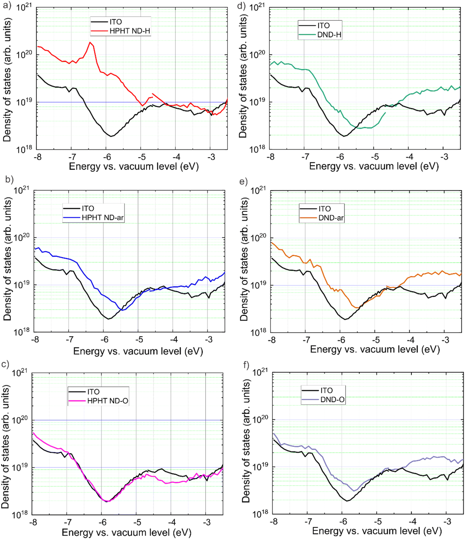 | ||
| Fig. 5 Band diagrams of HPHT and DND layers of NDs with as-received, hydrogenated, and oxidized surfaces obtained with the ER-EIS. DOS profiles are measured in the energy range from −8.0 to −2.5 eV (this is the limitation of the ER-EIS technique). The DOS of the ITO substrate is a black curve. | ||
The reference spectra are needed to distinguish the contribution of the investigated material itself and the substrate into DOS. In HPHT ND-H there is a pronounced DOS increase from −5.0 eV and below, indicating the VBM at −5.0 eV (Fig. 5a). This is in excellent agreement with the UPS results of the VBM value (−5.0 eV). Besides, there are additional electronic states in the bandgap of HPHT ND-H that are delocalised up to ∼−3 eV. From −3.0 eV to −2.6 eV there is a gap and above it, there is a method limitation. DFT calculations show that the sp2 phase on the ND surface introduces electronic states into the bandgap leading to the narrowing of the bandgap.83 Also, this ER-EIS result is in good agreement with UPS non-zero photoemission in the range between the Fermi level and VBM found in HPHT ND-H. Furthermore, the delocalisation of electronic states in HPHT ND-H can explain the conductivity of HPHT ND-H that distinguishes it from the other NDs.15
In HPHT ND-ar a steep exponential increase of the density of states in HPHT ND-ar compared to the substrate is observed between −5.5 eV and −6.8 eV. The exponential increase continues from −6.8 to −8.0 eV, however, it takes a less steep slope (Fig. 5b). Based on ER-EIS we can assign VBM either to −5.5 eV or −6.8 eV. Both values are higher than UPS VBM for HPHT ND-ar (−7.8 eV). In this regard, they also might originate from the intrabandgap electronic states caused by non-diamond C while the UPS VBM of HPHT ND-ar lies out of the energy range of the ER-EIS method.
In the spectrum of HPHT ND-O (Fig. 5c) no additional electronic states in the bandgap are present (at least until the measurement technique limit) which is obviously due to the low non-diamond content compared to HPHT ND-ar (in agreement with Raman spectra in Fig. 1). Moreover, HPHT ND-O even passivates the electronic states in the substrate (the DOS of HPHT ND-O on ITO goes below the DOS of bare ITO). The absence of the delocalised states in HPHT ND-O can explain the insulating properties of this material.15 The exponential increase of DOS at −7.0 eV of HPHT ND-O indicates the VBM position which reasonably agrees with the VBM determined via UPS (−7.5 eV).
Interestingly, ER-EIS spectra in the intrabandgap region of all the DNDs (Fig. 5d–f) look similar to each other and HPHT ND-ar. Raman spectra showed that the amorphous and isolated sp2 carbon fragments are a common structural feature in these samples. Most probably intrabandgap DOS in DNDs and HPHT ND-ar is dominated by amorphous carbon contribution while surface chemistry seems to have only a minor impact on these electronic states of DNDs in the ER-EIS measurements. As part of our future work, we are corroborating data differently by preparing a publication focusing solely on ER-EIS DOS data and calculated via density functional theory DOS of the ND models with the predefined surface groups to elucidate more strictly the effect of surface structure on the DOS of NDs.
3.5 Structure–electronic property relationships in nanodiamonds
After projecting the surface chemistry and carbon hybridisation states on the band diagram of the NDs, the regularities in electronic level shifts for NDs of different origins and surfaces are revealed (see Scheme 2). In Scheme 2 the following simplified classification is adopted, namely, sp3-Cbulk-H/-O refer to the bulk diamond in which C is solely sp3 hybridised and surface dangling bonds are saturated by H or O atoms. The values of the energy levels for the bulk diamond are taken from the literature.81,84 In the studied NDs there is always some fraction of non-diamond C due to fabrication (DND) and processing (DND and HPHT ND). In HPHT ND-H the non-diamond C is represented by an ordered sp2 C (see Fig. 1e and discussion), with the significant contribution of trans-polyacetylene chains; thus, {sp3ND + sp2C}-H depicts the structure and surface chemistry of HPHT ND-H (brackets in the label denote the hydrogenation/oxidation of both sp3ND and sp2C regions). DND-H contains a large amount of amorphous carbon (aC) in its structure whose impact on the optoelectronic properties of DND-H is significant according to ER-EIS. Thus, {sp3ND + aC}-H describes the structure and surface chemistry of DND-H. In oxidized species, the surface of HPHT ND-O differs from oxidized bulk diamond surface by the presence of the ordered sp2 phase. Thus, {sp3ND + sp2C}-O depicts the structure and surface chemistry of HPHT ND-O. The more defective nature of DND-O and HPHT ND-ar with pronounced amorphous C content is denoted as {sp3ND + aC}-O. DND-ar with the mixture of oxygen and hydrogen groups, and surface and volume defects are taken out of this classification so as not to complicate the picture.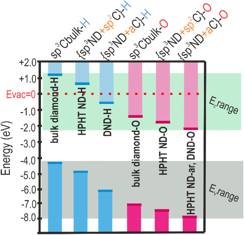 | ||
| Scheme 2 Simplified band energy position dependence on surface chemistry and C-hybridization of NDs. | ||
One of the trends in the energy levels' positions (VBM, CBM, EF) observed is several-eV (1.3–2.5 eV depending on the origin of the nanodiamonds) VBM downshift relative to the vacuum level after conversion from the fully hydrogenated to the fully oxidized surface (VBM downshifts in pairs HPHT ND-H and HPHT ND-O; DND-H and DND-O). Moreover, a clear effect of the carbon hybridization (ND structure) is observed. For the defined surface chemistry (H/O), the presence of non-diamond carbon downshifts the band edges compared to purely sp3 carbon hybridization in diamonds (compare energy levels of the bulk diamond with the ones of the materials with non-diamond C in Scheme 2). Notably, amorphous non-diamond C compared to the ordered sp2 C downshifts the ND band edges relative to the vacuum level by 0.1–1.3 eV depending on ND origin and surface chemistry (compare the VBM of both oxidized HPHT ND-O with structured sp2 and HPHT ND-ar with amorphous non-diamond C; hydrogenated HPHT ND-H with trans-polyacetylene chains and DND-H with amorphous non-diamond C).
Thus, the described edge energy level position with the knowledge of work function variation and DOS can facilitate the selection of suitable materials for such applications as photovoltaics and catalysis. Moreover, our experimental results provide evidence for the recent theoretical results on structured sp2 origin of continuous intrabandgap states83 and quantitative backup for the experimental studies on charge transfer in nanodiamond composites23,31 and resolve the discrepancies between the published results on ND optoelectronic properties (e.g. ND apparent bandgap differences30,85).
4 Conclusions
This work brings a comprehensive and quantitative approach to the understanding of the electronic properties of HPHT and detonation nanodiamonds with hydrogenated and oxidized surfaces. Band edges, the density of states, and work functions are determined purely experimentally by combining various spectroscopic methods, Kelvin probe and electrochemical impedance spectroscopy. The obtained data show that the positioning of the VBM of HPHT ND-H is high enough (−5.0 eV relative to the vacuum level), which together with the wide bandgap of NDs, assures that the CBM is positioned above the vacuum level (+0.5 eV). This way the NEA of HPHT ND-H is justified. Interestingly, HPHT ND-H contains the continuum of the electronic states inside the bandgap that, in addition to transfer doping, can contribute to electrical conductivity. We propose that a conjugated sp2 phase such as the trans-polyacetylene indicated by Raman spectroscopy introduces the intrabandgap states. DND-H does not possess NEA. We explain such a difference by the presence of amorphous carbon in DND-H that downshifts the VBM in DND-H compared to HPHT ND-H introducing positive electron affinity. The downshift of VBM relative to the vacuum level after amorphisation of the ND surface is in the 0.1–1.3 eV range (depending on the ND origin and surface chemistry) and after the fully hydrogenated surface oxidation it is in the 1.3–2.5 eV range (depending on the ND origin). The results can serve as a guide for selecting the suitable ND material for a particular application among the variety of NDs that differ in origin, surface chemistry and non-diamond carbon quality and content. For example, our work suggests that HPHT ND-H can be used for the photoreduction of N2 to ammonia and the production of solvated electrons in aqueous solutions. Also, this material combining high VBM with consequent high CBM vs. vacuum and electrical conductivity could find its application as a charge transport material in photovoltaics.Author contributions
DM conceptualisation, methodology, investigation, data & model visualisation, writing original draft; ASD – research discussion, manuscript review; JC – funding acquisition, manuscript review & editing; MS, FO and OR – UPS and XPS analysis, formal analysis and data visualisation review & editing; ES – FTIR; JP – hydrogenation of NDs; JK – Kelvin probe; VN – ER-EIS, formal analysis and data visualisation; SS – resources, research discussion, manuscript review & editing, funding acquisition; AK – resources, funding acquisition, manuscript review; HH – resources, research discussion, manuscript review & editing; BR – resources, research discussion, data processing and visualization, manuscript review & editing.Conflicts of interest
There are no conflicts of interest to declare.Acknowledgements
This work has been financially supported by the Czech Science Foundation project 20-20991J (GACR), the European Regional Development Fund project CZ.02.1.01/0.0/0.0/15 003/0000464 (CAP), and the Deutsche Forschungsgemeinschaft (DFG) via the DFG project number 431903417. We also acknowledge the use of the CzechNanoLab research infrastructure supported by the MEYS (LM2023051).References
- A. Krueger and D. Lang, Adv. Funct. Mater., 2012, 22, 890–906 CrossRef CAS.
- V. N. Mochalin, O. Shenderova, D. Ho and Y. Gogotsi, Nat. Nanotechnol., 2012, 7, 11–23 CrossRef CAS PubMed.
- N. Nunn, M. Torelli, G. McGuire and O. Shenderova, Curr. Opin. Solid State Mater. Sci., 2017, 21, 1–9 CrossRef CAS.
- L. Schmidlin, V. Pichot, M. Comet, S. Josset, P. Rabu and D. Spitzer, Diamond Relat. Mater., 2012, 22, 113–117 CrossRef CAS.
- W. S. Yeap, S. Chen and K. P. Loh, Langmuir, 2009, 25, 185–191 CrossRef CAS PubMed.
- A. Vlk, M. Ledinsky, A. Shiryaev, E. Ekimov and S. Stehlik, J. Phys. Chem. C, 2022, 126, 6318–6324 CrossRef CAS.
- J.-P. Boudou, J. Tisler, R. Reuter, A. Thorel, P. A. Curmi, F. Jelezko and J. Wrachtrup, Diamond Relat. Mater., 2013, 37, 80–86 CrossRef CAS.
- S. V. Bolshedvorskii, A. I. Zeleneev, V. V. Vorobyov, V. V. Soshenko, O. R. Rubinas, L. A. Zhulikov, P. A. Pivovarov, V. N. Sorokin, A. N. Smolyaninov, L. F. Kulikova, A. S. Garanina, S. G. Lyapin, V. N. Agafonov, R. E. Uzbekov, V. A. Davydov and A. V. Akimov, ACS Appl. Nano Mater., 2019, 2, 4765–4772 CrossRef CAS.
- V. A. Shershulin, V. S. Sedov, A. Ermakova, U. Jantzen, L. Rogers, A. A. Huhlina, E. G. Teverovskaya, V. G. Ralchenko, F. Jelezko and I. I. Vlasov, Phys. Status Solidi A, 2015, 212, 2600–2605 CrossRef CAS.
- N. Gibson, O. Shenderova, T. J. M. Luo, S. Moseenkov, V. Bondar, A. Puzyr, K. Purtov, Z. Fitzgerald and D. W. Brenner, Diamond Relat. Mater., 2009, 18, 620–626 CrossRef CAS.
- H. Huang, E. Pierstorff, E. Osawa and D. Ho, Nano Lett., 2007, 7, 3305–3314 CrossRef CAS PubMed.
- R. A. Shimkunas, E. Robinson, R. Lam, S. Lu, X. Xu, X.-Q. Zhang, H. Huang, E. Osawa and D. Ho, Biomaterials, 2009, 30, 5720–5728 CrossRef CAS PubMed.
- B. S. Miller, L. Bezinge, H. D. Gliddon, D. Huang, G. Dold, E. R. Gray, J. Heaney, P. J. Dobson, E. Nastouli, J. J. L. Morton and R. A. McKendry, Nature, 2020, 587, 588–593 CrossRef CAS PubMed.
- S. Stehlik, T. Glatzel, V. Pichot, R. Pawlak, E. Meyer, D. Spitzer and B. Rezek, Diamond Relat. Mater., 2016, 63, 97–102 CrossRef CAS.
- J. Čermák, H. Kozak, Š. Stehlík, V. Švrček, V. Pichot, D. Spitzer, A. Kromka and B. Rezek, MRS Adv., 2016, 1, 1105–1111 CrossRef.
- J. B. Cui, J. Ristein and L. Ley, Phys. Rev. Lett., 1998, 81, 429–432 CrossRef CAS.
- F. Maier, J. Ristein and L. Ley, Phys. Rev. B: Condens. Matter Mater. Phys., 2001, 64, 165411 CrossRef.
- J. Ristein, Surf. Sci., 2006, 600, 3677–3689 CrossRef CAS.
- C. A. Feigl, B. Motevalli, A. J. Parker, B. Sun and A. S. Barnard, Nanoscale Horiz., 2019, 4, 983–990 RSC.
- F. Buchner, T. Kirschbaum, A. Venerosy, H. Girard, J.-C. Arnault, B. Kiendl, A. Krueger, K. Larsson, A. Bande, T. Petit and C. Merschjann, Nanoscale, 2022, 14, 17188–17195 RSC.
- X. Duan, W. Tian, H. Zhang, H. Sun, Z. Ao, Z. Shao and S. Wang, ACS Catal., 2019, 9, 7494–7519 CrossRef CAS.
- L. Ginés, S. Mandal, A.-I.-A. Ashek-I-Ahmed, C.-L. Cheng, M. Sow and O. A. Williams, Nanoscale, 2017, 9, 12549–12555 RSC.
- J. Henych, Š. Stehlík, K. Mazanec, J. Tolasz, J. Čermák, B. Rezek, A. Mattsson and L. Österlund, Appl. Catal., B, 2019, 259, 118097 CrossRef CAS.
- D. M. Jang, Y. Myung, H. S. Im, Y. S. Seo, Y. J. Cho, C. W. Lee, J. Park, A.-Y. Jee and M. Lee, Chem. Commun., 2012, 48, 696–698 RSC.
- H. Wang, Y.-K. Tzeng, Y. Ji, Y. Li, J. Li, X. Zheng, A. Yang, Y. Liu, Y. Gong, L. Cai, Y. Li, X. Zhang, W. Chen, B. Liu, H. Lu, N. A. Melosh, Z.-X. Shen, K. Chan, T. Tan, S. Chu and Y. Cui, Nat. Nanotechnol., 2020, 15, 131–137 CrossRef CAS PubMed.
- S. Yu, N. Yang, H. Zhuang, J. Meyer, S. Mandal, O. A. Williams, I. Lilge, H. Schönherr and X. Jiang, J. Phys. Chem. C, 2015, 119, 18918–18926 CrossRef CAS.
- Y. Liu, Y.-K. Tzeng, D. Lin, A. Pei, H. Lu, N. A. Melosh, Z.-X. Shen, S. Chu and Y. Cui, Joule, 2018, 2, 1595–1609 CrossRef CAS.
- K. Jothiramalingam Sankaran, S. Kunuku, B. Sundaravel, P.-Y. Hsieh, H.-C. Chen, K.-C. Leou, N.-H. Tai and I.-N. Lin, Nanoscale, 2015, 7, 4377–4385 RSC.
- Y. L. Zhong, A. Midya, Z. Ng, Z.-K. Chen, M. Daenen, M. Nesladek and K. P. Loh, J. Am. Chem. Soc., 2008, 130, 17218–17219 CrossRef CAS PubMed.
- A. Nagata, O. K. U. Takeo, K. Kikuchi, A. Suzuki, Y. Yamasaki and E. Osawa, Prog. Nat. Sci., 2010, 20, 38–43 CrossRef.
- D. Miliaieva, P. Matunova, J. Cermak, S. Stehlik, A. Cernescu, Z. Remes, P. Stenclova, M. Muller and B. Rezek, Sci. Rep., 2021, 11, 590 CrossRef CAS PubMed.
- L. Cheng, S. Zhu, X. Ouyang and W. Zheng, Diamond Relat. Mater., 2023, 132, 109638 CrossRef CAS.
- T. Kondo, I. Neitzel, V. N. Mochalin, J. Urai, M. Yuasa and Y. Gogotsi, J. Appl. Phys., 2013, 113, 214307 CrossRef.
- K.-Y. Niu, H.-M. Zheng, Z.-Q. Li, J. Yang, J. Sun and X.-W. Du, Angew. Chem., 2011, 123, 4185–4188 CrossRef.
- P. Matunová, V. Jirásek and B. Rezek, Phys. Status Solidi B, 2019, 1900176 CrossRef.
- A. A. Fokin and P. R. Schreiner, Mol. Phys., 2009, 107, 823–830 CrossRef CAS.
- S. Osswald, G. Yushin, V. Mochalin, S. O. Kucheyev and Y. Gogotsi, J. Am. Chem. Soc., 2006, 128, 11635–11642 CrossRef CAS PubMed.
- V. I. Korepanov, H. Hamaguchi, E. Osawa, V. Ermolenkov, I. K. Lednev, B. J. M. Etzold, O. Levinson, B. Zousman, C. P. Epperla and H.-C. Chang, Carbon, 2017, 121, 322–329 CrossRef CAS.
- S. Osswald, M. Havel, V. Mochalin, G. Yushin and Y. Gogotsi, Diamond Relat. Mater., 2008, 17, 1122–1126 CrossRef CAS.
- S. Stehlik, M. Varga, M. Ledinsky, D. Miliaieva, H. Kozak, V. Skakalova, C. Mangler, T. J. Pennycook, J. C. Meyer, A. Kromka and B. Rezek, Sci. Rep., 2016, 6, 38419 CrossRef CAS PubMed.
- S. Stehlik, M. Mermoux, B. Schummer, O. Vanek, K. Kolarova, P. Stenclova, A. Vlk, M. Ledinsky, R. Pfeifer, O. Romanyuk, I. Gordeev, F. Roussel-Dherbey, Z. Nemeckova, J. Henych, P. Bezdicka, A. Kromka and B. Rezek, J. Phys. Chem. C, 2021, 125, 5647–5669 CrossRef CAS.
- V. I. Korepanov, H. Hamaguchi, E. Osawa, V. Ermolenkov, I. K. Lednev, B. J. M. Etzold, O. Levinson, B. Zousman, C. P. Epperla and H.-C. Chang, Carbon, 2017, 121, 322–329 CrossRef CAS.
- K. Turcheniuk and V. N. Mochalin, Nanotechnology, 2017, 28, 252001 CrossRef CAS PubMed.
- O. A. Williams, J. Hees, C. Dieker, W. Jäger, L. Kirste and C. E. Nebel, ACS Nano, 2010, 4, 4824–4830 CrossRef CAS PubMed.
- T. Kondo, I. Neitzel, V. N. Mochalin, J. Urai, M. Yuasa and Y. Gogotsi, J. Appl. Phys., 2013, 113, 214307 CrossRef.
- A.-I. Ahmed, S. Mandal, L. Gines, O. A. Williams and C.-L. Cheng, Carbon, 2016, 110, 438–442 CrossRef CAS.
- S. Stehlik, M. Varga, P. Stenclova, L. Ondic, M. Ledinsky, J. Pangrac, O. Vanek, J. Lipov, A. Kromka and B. Rezek, ACS Appl. Mater. Interfaces, 2017, 9, 38842–38853 CrossRef CAS PubMed.
- J. Mikesova, D. Miliaieva, P. Stenclova, M. Kindermann, T. Vuckova, M. Madlikova, M. Fabry, V. Veverka, J. Schimer, P. Krejci, S. Stehlik and P. Cigler, Carbon, 2022, 195, 372–386 CrossRef CAS.
- L. Saoudi, H. A. Girard, E. Larquet, M. Mermoux, J. Leroy and J.-C. Arnault, Carbon, 2023, 202, 438–449 CrossRef CAS.
- K. Kolarova, I. Bydzovska, O. Romanyuk, E. Shagieva, E. Ukraintsev, A. Kromka, B. Rezek and S. Stehlik, Diamond Relat. Mater., 2023, 109754 CrossRef CAS.
- J. Tauc, R. Grigorovici and A. Vancu, Phys. Status Solidi B, 1966, 15, 627–637 CrossRef CAS.
- E. A. Davis and N. F. Mott, Philos. Mag., 1970, 22, 0903–0922 CrossRef CAS.
- A. M. Shing, Y. Tolstova, N. S. Lewis and H. A. Atwater, Appl. Phys. A, 2017, 123, 735 CrossRef CAS.
- V. Nádaždy, F. Schauer and K. Gmucová, Appl. Phys. Lett., 2014, 105, 142109 CrossRef.
- S. Volk, N. Yazdani, E. Sanusoglu, O. Yarema, M. Yarema and V. Wood, J. Phys. Chem. Lett., 2018, 9, 1384–1392 CrossRef CAS PubMed.
- S. Turner, O. Shenderova, F. D. Pieve, Y. Lu, E. Yücelen, J. Verbeeck, D. Lamoen and G. V. Tendeloo, Phys. Status Solidi A, 2013, 210, 1976–1984 CrossRef CAS.
- O. S. Kudryavtsev, R. H. Bagramov, A. M. Satanin, A. A. Shiryaev, O. I. Lebedev, A. M. Romshin, D. G. Pasternak, A. V. Nikolaev, V. P. Filonenko and I. I. Vlasov, Nano Lett., 2022, 22, 2589–2594 CrossRef CAS PubMed.
- E. Ekimov, A. A. Shiryaev, Y. Grigoriev, A. Averin, E. Shagieva, S. Stehlik and M. Kondrin, Nanomaterials, 2022, 12, 351 CrossRef CAS PubMed.
- A. Wolcott, T. Schiros, M. E. Trusheim, E. H. Chen, D. Nordlund, R. E. Diaz, O. Gaathon, D. Englund and J. S. Owen, J. Phys. Chem. C, 2014, 118, 26695–26702 CrossRef CAS PubMed.
- S. Ji, T. Jiang, K. Xu and S. Li, Appl. Surf. Sci., 1998, 133, 231–238 CrossRef CAS.
- T. Petit, L. Puskar, T. Dolenko, S. Choudhury, E. Ritter, S. Burikov, K. Laptinskiy, Q. Brzustowski, U. Schade, H. Yuzawa, M. Nagasaka, N. Kosugi, M. Kurzyp, A. Venerosy, H. Girard, J.-C. Arnault, E. Osawa, N. Nunn, O. Shenderova and E. F. Aziz, J. Phys. Chem. C, 2017, 121, 5185–5194 CrossRef CAS.
- S. Stehlik, M. Varga, M. Ledinsky, V. Jirasek, A. Artemenko, H. Kozak, L. Ondic, V. Skakalova, G. Argentero, T. Pennycook, J. C. Meyer, A. Fejfar, A. Kromka and B. Rezek, J. Phys. Chem. C, 2015, 119, 27708–27720 CrossRef CAS PubMed.
- A. P. Koshcheev, Russ. J. Gen. Chem., 2009, 79, 2033–2044 CrossRef CAS.
- J. O. Orwa, K. W. Nugent, D. N. Jamieson and S. Prawer, Phys. Rev. B: Condens. Matter Mater. Phys., 2000, 62, 5461–5472 CrossRef CAS.
- S. Osswald, V. N. Mochalin, M. Havel, G. Yushin and Y. Gogotsi, Phys. Rev. B: Condens. Matter Mater. Phys., 2009, 80, 075419 CrossRef.
- A. C. Ferrari and J. Robertson, Philos. Trans. R. Soc., A, 2004, 362, 2477–2512 CrossRef CAS PubMed.
- S. Turner, O. I. Lebedev, O. Shenderova, I. I. Vlasov, J. Verbeeck and G. Van Tendeloo, Adv. Funct. Mater., 2009, 19, 2116–2124 CrossRef CAS.
- M. Mermoux, A. Crisci, T. Petit, H. A. Girard and J.-C. Arnault, J. Phys. Chem. C, 2014, 118, 23415–23425 CrossRef CAS.
- M. Mermoux, S. Chang, H. A. Girard and J.-C. Arnault, Diamond Relat. Mater., 2018, 87, 248–260 CrossRef CAS.
- K. V. Reich, JETP Lett., 2011, 94, 22 CrossRef CAS.
- H. K. Jeong, C. Yang, B. S. Kim and K. Kim, Europhys. Lett., 2010, 92, 37005 CrossRef.
- J. C. Zuaznabar-Gardona and A. Fragoso, Synth. Met., 2020, 266, 116434 CrossRef CAS.
- H. Ago, T. Kugler, F. Cacialli, W. R. Salaneck, M. S. P. Shaffer, A. H. Windle and R. H. Friend, J. Phys. Chem. B, 1999, 103, 8116–8121 CrossRef CAS.
- V. Chakrapani, J. C. Angus, A. B. Anderson, S. D. Wolter, B. R. Stoner and G. U. Sumanasekera, Science, 2007, 318, 1424–1430 CrossRef CAS PubMed.
- C. E. Nebel, Science, 2007, 318, 1391–1392 CrossRef CAS PubMed.
- W. Chen, D. Qi, X. Gao and A. T. S. Wee, Prog. Surf. Sci., 2009, 84, 279–321 CrossRef CAS.
- K. G. Crawford, I. Maini, D. A. Macdonald and D. A. J. Moran, Prog. Surf. Sci., 2021, 96, 100613 CrossRef CAS.
- F. Maier, M. Riedel, B. Mantel, J. Ristein and L. Ley, Phys. Rev. Lett., 2000, 85, 3472–3475 CrossRef CAS PubMed.
- N. Bauer, J. Phys. Chem., 1960, 64, 833–837 CrossRef CAS.
- J. B. Cui, J. Ristein and L. Ley, Phys. Rev. Lett., 1998, 81, 429–432 CrossRef CAS.
- F. Maier, J. Ristein and L. Ley, Phys. Rev. B: Condens. Matter Mater. Phys., 2001, 64, 165411 CrossRef.
- M. Krátká, A. Kromka, E. Ukraintsev, M. Ledinský, A. Brož, M. Kalbacova and B. Rezek, Sens. Actuators, B, 2012, 166–167, 239–245 CrossRef.
- F. Buchner, T. Kirschbaum, A. Venerosy, H. Girard, J.-C. Arnault, B. Kiendl, A. Krueger, K. Larsson, A. Bande, T. Petit and C. Merschjann, Nanoscale, 2022, 14, 17188–17195 RSC.
- C. E. Nebel, B. Rezek, D. Shin and H. Watanabe, Phys. Status Solidi A, 2006, 203, 3273–3298 CrossRef CAS.
- N. Giambrone, M. McCrory, A. Kumar and M. K. Ram, Thin Solid Films, 2016, 615, 226–232 CrossRef CAS.
Footnote |
| † Electronic supplementary information (ESI) available. See DOI: https://doi.org/10.1039/d3na00205e |
| This journal is © The Royal Society of Chemistry 2023 |