DOI:
10.1039/D3NA00147D
(Paper)
Nanoscale Adv., 2023,
5, 4424-4434
Spatial modulation of scalable nanostructures by combining maskless plasmonic lithography and grayscale-patterned strategy
Received
6th March 2023
, Accepted 23rd June 2023
First published on 26th June 2023
Abstract
Nanolithography techniques providing good scalability and feature size controllability are of great importance for the fabrication of integrated circuits (IC), MEMS/NEMS, optical devices, nanophotonics, etc. Herein, a cost-effective, easy access, and high-fidelity patterning strategy that combines the high-resolution capability of maskless plasmonic lithography with the spatial morphology controllability of grayscale lithography is proposed to generate the customized pattern profile from microscale to nanoscale. Notably, the scaling effect of gap size in plasmonic lithography with a contact bowtie-shaped nanoaperture (BNA) is found to be essential to the rapid decay characteristics of an evanescent field, which leads to a wide energy bandwidth of the required optimal dose to record pattern in per unit volume, and hence, achieves the volumetrically scalable control of the photon energy deposition in the space more precisely. Based on the proper calibration and cooperation of pattern width and depth, a grayscale-patterned map is designed to compensate for the dose difference caused by the loss of the high spatial frequency component of the evanescent field. A Lena nanostructure with varying feature sizes by spatially modulating the exposure dose distribution was successfully demonstrated, and besides, we also successfully generated a microlens array (MLA) with high uniformity. The practical patterning method makes plasmonic lithography significant in the fabrication of functional nanostructures with high performance, including metasurfaces, plasmonics, and optical imaging systems.
1 Introduction
With the rapid advancement in lithography techniques, the demand for precise control of feature size and spatial morphology for nanopatterning is eminent.1–5 This is principally because the performance characteristics of nanodevices are highly sensitive to the critical dimensions of nanostructures. Consequently, it is essential to achieve arbitrary modulation of nanoscale feature size with high fidelity in the lithographic process.6–11 Thus far, the mainstream approaches for accurate nanofabrication with arbitrary shapes are photolithography and laser direct write lithography.12–22 Photolithography can provide large scale patterning, and laser direct write lithography has shown its great potential in the fabrication of complex three-dimensional micro–nano structures. However, they suffer from limited pattern resolution by the intrinsic property of light diffraction. Although electron-beam lithography (EBL) and focused ion beam (FIB) milling are capable of high-resolution patterning, they are costly, and the patterning speed limits their throughput.23,24 For the high-throughput nanoimprint lithography, the imprint templates are extremely expensive and the pattern fidelity heavily relies on the master imprint mold.25,26 Interference lithography is also capable of generating high-resolution periodic structures with high throughput, but it is not suited for arbitrarily shaped patterns.27,28 Therefore, developing a scalable nanolithographic strategy that simultaneously satisfies (1) low cost, high-resolution, and high pattern fidelity and (2) good feature size controllability with various shapes is still a challenge in the nanotechnology community.
Maskless plasmonic lithography is a cost-effective and promising strategy for top-down scalable nanomanufacturing because it can provide high pattern resolution, larger freedom of pattern shape design, remove the need for mask fabrication, and yield both time and cost savings for the fast prototyping of exposure system.29,30 However, the precise control of feature size during the patterning process still faces serious challenges. By employing a metallic bowtie-shaped nanoaperture (BNA) as the beam spot generator, which can induce the surface plasmon waves (SPWs) and directly achieve a wavelength much smaller than that of the incident light, the resolution of plasmonic lithography has been successfully scaled down to sub-10 nm.31,32 Moreover, the scanning speed of the maskless plasmonic lithography can be up to mm s−1 order, which is high enough for use in actual industry fabrication processes.29 Recently, the research scope of plasmonic lithography has been focused on practical applications, and the feasibility of applying plasmonic lithography to micro–nano surface patterning has been further extended from 1- to 2.5-dimension.33 The final pattern accuracy has also been effectively improved to over 90% using near-field optical proximity correction (OPC) methods on the basis of the evanescent nature of the SPWs.32,34 Additionally, patterns with large aspect ratios have been achieved using a hybrid plasmonic waveguide exposure system to amplify the plasmonic optical evanescent field in the photoresist (PR) layer.35 Almost all of the previously reported results show that the decay characteristics of the SPWs critically affect the final pattern features in plasmonic lithography, but their corresponding relation has not yet been intensively studied. Therefore, to realize the plasmonic lithography for scalable nanofabrication, the more detailed evanescent components confined by the spatial modulation of exposure dose for multi-scale arbitrary patterning need to be captured and controlled accurately to reconstruct a faithful replica of the desired patterns with high quality and thereby achieve the precise manipulation of feature size in nanoscale.
Grayscale-patterned method is a powerful approach for generating the gradient height structures in the PR layer, which refers to using a variable-dose exposure to control the pattern depth (different exposure dose makes differential pattern depth of exposed PR across the surface).36–39 Significantly, the advances in good controllability of feature size modulation make grayscale lithography potentially capable of meeting the increasing demand for high-precision micro–nano 3D manufacturing. Unfortunately, achieving nanometer features and resolution in grayscale lithography is limited by light diffraction. Because the grayscale lithography uses diffraction to modulate the amplitude of the intensity by controlling the pixels and pitches, each variable intensity is regarded as a gray level, whereas the number of the gray levels is determined by the lithographic resolution.
In the present study, we develop a practical and effective manufacturing technique for scalable nanofabrication that provides a simple yet versatile and cost-effective patterning strategy by combining the plasmonic lithography and the grayscale-patterned method. The patterning method combines the subwavelength feature size generation capability of plasmonic lithography with the precise feature size manipulation capability of grayscale lithography. When aiming at scalable nanostructuring, we emphasize that obtaining good width features is as significant as much as obtaining good depth features. Hence, we theoretically investigate the rapid decaying features of SPWs at the lateral and vertical directions of a plasmonic BNA, respectively. Interestingly, it is found that the scaling behavior of near-field intensity decay can yield a wide bandwidth of required exposure dose per unit volume by contrasting the photoresist contrast curves of plasmonic lithography with those of conventional optical lithography. Although this unique feature enables plasmonic lithography to control the patterning profile more precisely, in reality, it is also a major optical cause of pattern distortion due to the loss of the high spatial frequency component of SPWs. To compensate for the disparity between the desired shape and the patterning result, a grayscale-patterned map is designed to spatially modulate the various feature sizes. To show the potential of the novel lithographic method, Lena and MLA micro–nano structures have been demonstrated with high resolution and high uniformity. Therefore, plasmonic lithography not only allows fast prototyping with precisely modulated feature size but also exhibits the versatility of scalable manufacturing.
2 Good feature size controllability in maskless plasmonic lithography
2.1 Theoretical analysis of the scaling behavior in plasmonic BNA
The patterning process of maskless plasmonic lithography with a scanning contact probe is schematically illustrated in Fig. 1. Typically, the plasmonic lithographic process consists of exposing PR by a photon beam source generated by a metallic BNA and subsequently developing the PR for pattern transfer. The profile of the final exposed pattern in the PR layer is spatially modulated via the exposure dose distribution.34,40,41 It is important to note that the exposure dose distribution (energy deposited in the PR layer) is determined by the convolution between an exposure dose map (feature size modulation) and a point spread function (PSF), which is complex and shows how the photon energy is distributed throughout the PR when a single spot is exposed. Hence, in order to achieve high pattern quality, estimation of the PSF with accuracy and efficiency is crucial during the patterning process. Unlike the conventional optical lithography, whose pattern is generated by far-field diffraction, the pattern profile created by plasmonic lithography is mainly determined by the near-field intensity of PSF (Ipsf). Because the PSF in plasmonic lithography has an asymmetric field structure identified by both surface waves (near-field waves, Inear-field) and space waves (far-field waves, Ifar-field) emerging from the plasmonic BNA, complex decaying characteristics coexist with the evanescent field region.42–45 As a consequence, the PSF is difficult to be directly described with exact functions. Nevertheless, for simplicity of analytic approach, the decay behavior of the PSF can be investigated numerically and theoretically.| | | Ipsf(x,y,z) = Inear-field(x,y,z) + Ifar-field(x,y,z) | (1) |
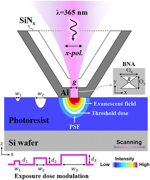 |
| | Fig. 1 Schematic of the basic exposure principle of the maskless plasmonic lithography system with a scanning metallic BNA. The optical source, which is a linearly x-polarized laser with λ = 365 nm, is incident on a metallic BNA. The geometry of the BNA is given by the dimension Ox = Oy = 150 nm with various gap sizes (g) from 4 to 24 nm. Exposure dose modulation is adopted to achieve the precise manipulation of feature size for multi-scale nanopatterning. The color map shows the intensity distribution of the generated pattern along the z-direction. | |
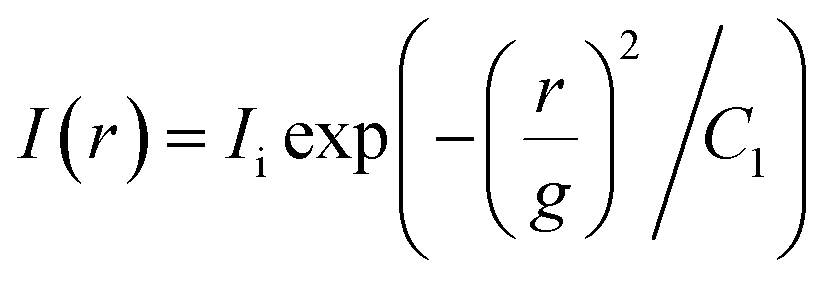
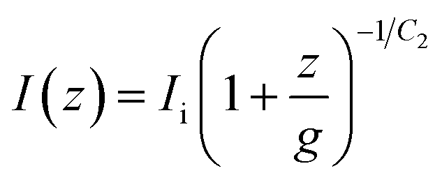
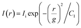
To study the decay characteristics of the PSF, a finite differential time domain (FDTD, ansys lumerical v2021) calculation is performed to obtain the three-dimensional electronic field distribution in the plasmonic lithography exposure system. A transverse magnetic (TM) polarized Gaussian beam with λ = 365 nm is illuminated on the metallic BNA. At this illumination wavelength, the permittivities of Al, SiNx, and PR are εAl = −19.4 + 3.6i, εSiNx = 2.1, and εPR = 2.9, respectively. To quantitatively research the decay features of PSF generated by the plasmonic BNA, and further investigate their effects on the pattern width and depth, the transmitted intensity profile through the different gap sizes at the gap center along the y-direction and z-direction are separately analyzed. As shown in Fig. 2a and c, the normalized intensity distributions are calculated as functions of lateral distance (r) and vertical distance (z) for several BNA with ridge gaps of 4, 14, and 24 nm, respectively. To express the non-propagating properties of the evanescent field in the different directions, previous research works have shown that the intensity distribution in the lateral direction (I(r)) can be described with a Gaussian-based function and a hyperbolic decay function can be used to describe the intensity distribution in the vertical direction (I(z)).29,46
| |  | (2) |
| |  | (3) |
where
r is the radius from the BNA center,
g is the gap size of BNA,
z is the distance away from the BNA exit,
Ii is the intensity at
r =
z = 0,
C1 is the Gaussian fitting parameter, and
C2 is the decay constant in the
z-direction. The lateral and vertical normalized intensity distributions generated by the plasmonic BNA with gap sizes of 4, 14, and 24 nm are also plotted as functions of the
r/
g ratio and the
z/
g ratio in
Fig. 2b and d to compare the theoretical models with the simulations, respectively. They show that the proposed theoretical models of lateral and vertical intensity distribution agree well with the simulation data. From the fitting processes in
eqn (2) and (3), we obtained
C1 = 0.8168 ± 0.0075 and
C2 = 0.3289 ± 0.0095. It is notable that the decay trends in the lateral and vertical directions exhibit the scaling behavior,
i.e., the decay trend becomes independent of the gap size of BNA on account of this scaling. The results also clearly indicate that the scaling behavior of the plasmonic BNA will play a critical role in determining the patterning quality. Particularly, as the feature size of nanostructures approaches the resolution limit, the decay influence needs to be evaluated precisely to estimate the final pattern profile.
 |
| | Fig. 2 Scaling behavior of evanescent-field decaying feature in plasmonic BNA. (a) The calculated normalized intensity distribution as a function of lateral distance r with gap sizes of 4, 14, and 24 nm. (b) Plot of the normalized intensity distribution versus the r/g ratio, showing that the scaled data points for the different ridge gap sizes follow the same tendency. The solid black line is obtained with a Gaussian-based fitting function. (c) The normalized intensity distribution as a function of vertical distance z with gap sizes of 4, 14 and 24 nm. (d) Plot of the normalized intensity distribution versus the z/g ratio, showing that with increasing the gap size of BNA, the magnitude of the normalized intensity at a given distance z increases. The solid black line is obtained with a hyperbolic function model. | |
2.2 Wider bandwidth of exposure dose in plasmonic lithography
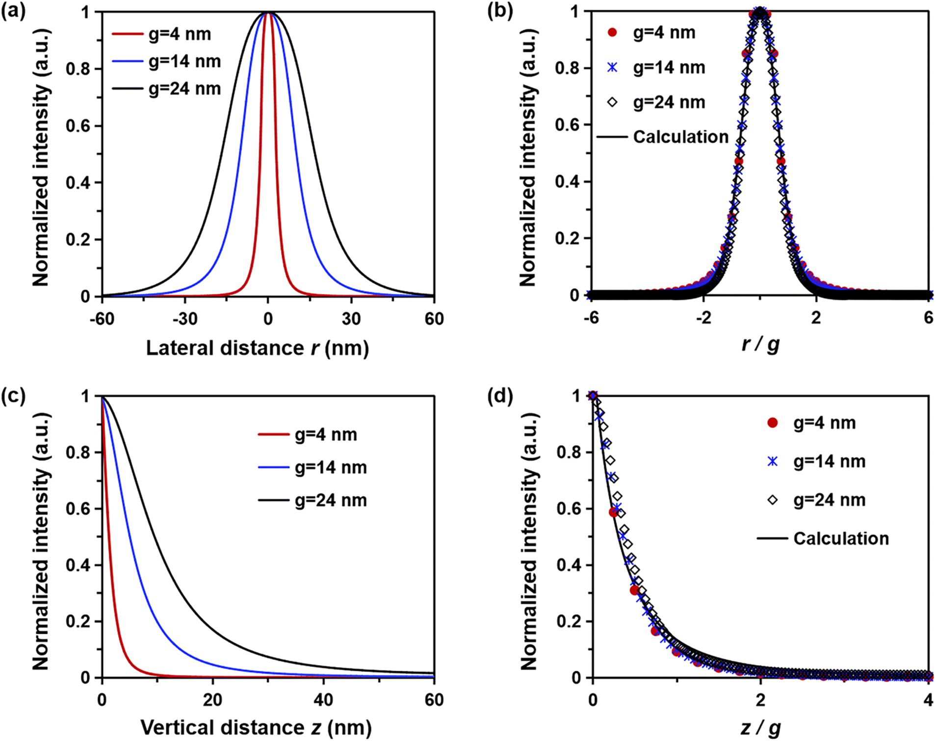
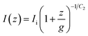
Typically, the photoresist contrast curve is an important parameter for determining the final pattern profile because it determines the required exposure dose at the pattern edge position and is usually obtained by the thickness versus dose function in conventional optical lithography. However, the photoresist contrast curve of plasmonic lithography is greatly influenced by the rapid decay characteristics of the evanescent field and can also be estimated via the width versus dose relationship. Unlike the photoresist contrast of a laser direct writing system (γfar), which is calculated by using the formula γ = [ln(Dcl/Dth)]−1, Dth is the threshold dose, and Dcl is the clearing dose. Dth and Dcl are defined as the minimum exposure doses required for the PR reacting to the light and for complete PR removal, respectively. Typically, the local exposure dose is determined by the equation Dex = It, where I is the total intensity of the field, and t is the exposure time. Our previous works have demonstrated that the photoresist contrast of plasmonic lithography (γnear) is approximately equal to the evanescent field-induced photoresist contrast (γdecay), which is mainly dependent on the decay constant of the evanescent field.29,40| | | γnear−1 = γfar−1 + γdecay−1 | (4) |
Thus, to further investigate the effect of the decay characteristics of the evanescent field on the final pattern profile, the photoresist contrast curves are measured in the vertical direction of the generated spot-mapping patterns. By varying the normalized value of the exposure dose from 1 to 6 in increments of 0.5, spot pattern lines were fabricated on one sample. After the exposure, the Si wafer was developed for 2 min in KOH solution, followed by rinsing with distilled water for 20 s. During the measurement step, atomic force microscopy (AFM; Park systems, XE-100) was used to obtain the morphology of the spot mapping pattern. As shown in Fig. 3a, the measured photoresist contrast curve of the plasmonic lithography is wider than that of the laser direct writing system. The photoresist contrast of the laser direct writing system was measured to be γfar ∼ 5.5207, but the measured photoresist contrast of plasmonic lithography contrast varied with the distance and was much smaller than that in the laser direct writing system, i.e., 0.0835 ≤ γnear ≤ 0.1306. The unique feature can yield a wider bandwidth of the required exposure dose per unit volume for plasmonic lithography than that in the other lithography techniques. A wide dose bandwidth can lead to being more accurate in achieving volumetrically scalable control of the photon energy in space, as illustrated in Fig. 3b. By analyzing these results, we can conclude that the rapidly decreasing behavior of intensity in the plasmonic lithography can be an advantage to achieve the high quality top-down scalable nanostructuring because it allows the feature size modulation of multi-scale nanopatterning to be more precise, especially in nanoscale.
 |
| | Fig. 3 Estimation of photoresist contrasts. (a) The photoresist contrast curves of (line with triangles) laser direct writing system, and (line with squares) plasmonic lithography system. (b) Diagrams of dose bandwidth in the space for (black dots) laser direct writing system and (red dots) plasmonic lithography system. The initial and last points are indicated by black and yellow circles, respectively. | |
3 Grayscale patterning method
3.1 Concept of grayscale-patterned strategy in plasmonic lithography
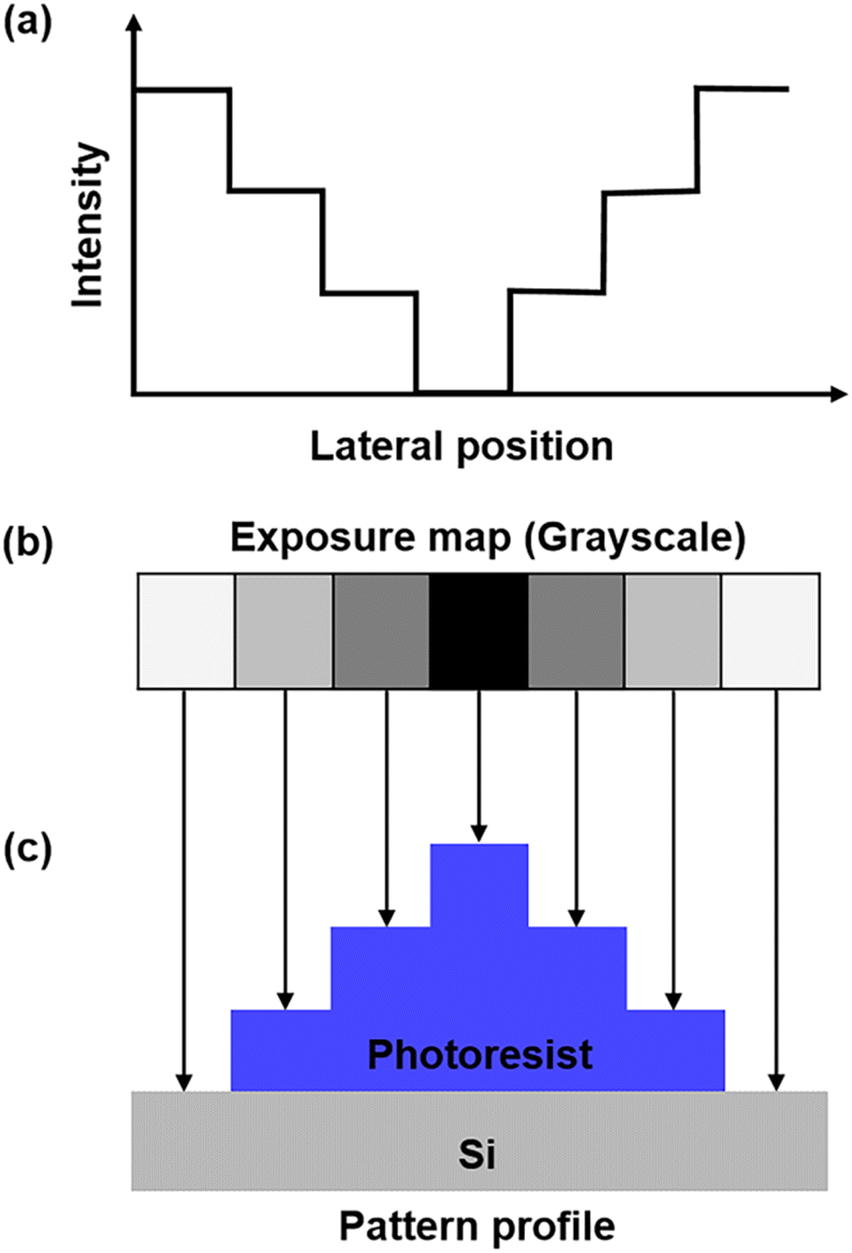
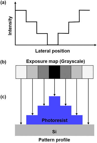
When the plasmonic lithography system records multi-scale target patterns with arbitrary shapes, the analog target pattern image is converted into a digital grayscale exposure map. As schematically shown in Fig. 4, the grayscale-patterned exposure map makes it possible to spatially modulate the intensity distribution according to the surface profile of the customized target pattern. Fig. 4a shows the modulation of the exposure intensity, which is obtained through different grayscale values, with an aim to modulate the depth and width of the final pattern in the PR layer. Fig. 4b and c show the schematic of the grayscale-patterned method for a positive PR, where the rectangles in Fig. 4b correspond to the digital grayscale exposure map design, and the grayscale value of each rectangular pixel corresponds to the required intensity when exposing these patterns. Note that each individual rectangle in the exposure map can be exposed with a specific grayscale value, and each grayscale value corresponds to one feature size of exposure dose where the clearing dose is obtained in the development process. The larger the grayscale value, the larger the exposure intensity and thereby the larger the depth of the final pattern in the PR layer. By gradual modulation of the grayscale values from one pixel to another, a scalable pattern profile with multi feature size is obtained in the PR layer, as shown in Fig. 4c. Therefore, in principle, almost any arbitrary scalable profiles can be patterned by using plasmonic lithography, whether using positive PR or negative PR.
 |
| | Fig. 4 Schematic showing the grayscale-patterned strategy. (a) The exposure intensity with various feature sizes. (b) The exposure dose map with feature size modulation. (c) Final pattern profile on the PR layer after the development process. The larger the size of the black arrow, the higher is the exposure dose and vice versa. | |
3.2 Dose calibration for the precise feature size modulation
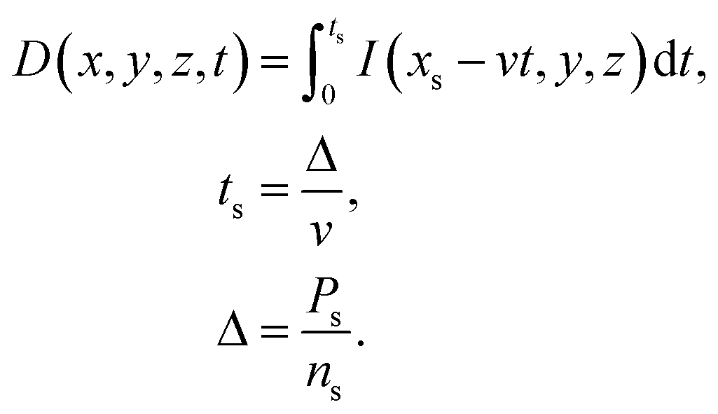
To achieve the goal of precise grayscale control in plasmonic lithography, the relationship between the intensity and the grayscale value essentially needs to be estimated. In plasmonic lithography with a scanning BNA, continuous exposure is available along the scanning direction within a given line. During the exposure process, the input laser power is kept constant as well as focusing setting. Thus, the accumulated dose (D) along the scanning direction within the laser On-pixel region can be expressed as follows:| |  | (5) |
where I(x,y,z,t) is the designed grayscale intensity distribution, t is the exposure time, xs is the patterning length along the scanning direction, v is the scanning speed, ts is determined by the scanning speed and the sub-pixel size (Δ), and Δ is determined by the pixel size (Ps) and the step level (ns). During a scan within a pixel size, the maximum number of laser On-unit times depends on ns; for instance, when ns = 5, the maximum number of laser On-unit times is 5. As illustrated in Fig. 5a, the grayscale dose control is based on the spatial modulation of laser pulse width, which enable 256 grayscale values or more in theory. For accurately controlling the pattern feature size, a discrete sub-pixel is used as an assist feature to deliver the proper dose to the adjacent region and not appear as a developed pattern. Moreover, previous works have shown that the assist sub-pixel can relax the shape complexity of the PSF and then play a role in compensating the feature error induced by the decaying characteristics of the evanescent field.32,34 However, the obtained pattern features of the grayscale values really depend on many factors, primarily the aerial image intensity for each grayscale value, the photoresist contrast, the development time, and the initial PR thickness. Unfortunately, accurate general theoretical formulas for describing the nonlinear relationships between them are lacking. Hence, a reliable calibration curve that can provide a precise relationship between the pattern feature size and the grayscale value is adopted and further used to identify the lithographic process window for grayscale-patterned method. By varying the exposure time level, we obtained the calibration curves of pattern depth and width with different step levels from 5 to 25, as shown in Fig. 5b and c, respectively. These results indicate that the relationship between the exposure dose and the grayscale value, and the relationships between the exposure dose and the pattern depth and width are all nonlinear. According to these calibration curves, an accurate grayscale exposure map can be generated to compensate the pattern distortions caused by these nonlinear effects. Therefore, we can conclude that by using the one-step maskless plasmonic lithography, one can precisely control the grayscale value to modulate the optimal exposure dose required for the scalable fabrication of micro–nano structures with arbitrary shapes.
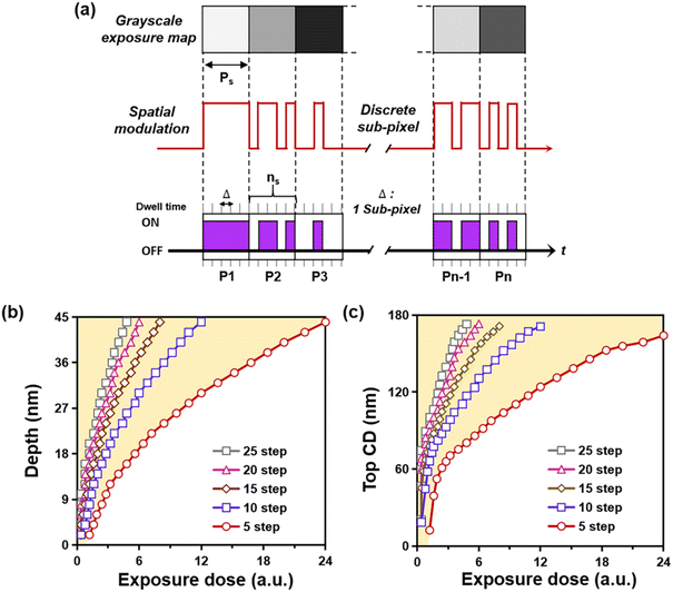 |
| | Fig. 5 Spatial modulation of pattern feature sizes using plasmonic lithography and calibration curves of exposure dose. (a) Schematic of spatial modulation of pattern feature size using grayscale-patterned exposure map. (b) Calibration curves of the pattern depth depending on the exposure dose with various laser On-time step levels. (c) Calibration curves of the pattern width depending on the exposure dose with various laser On-time step levels. | |
4 Results and discussion
4.1 Experimental results of scalable nanostructures
The main focus of our experiments was to demonstrate the feasibility of the grayscale-patterned method. Thus, a valid method is to find a reliable calibration curve that can provide a precise relationship between the pattern features and the grayscale values. Line mapping patterns were recorded on a positive PR using plasmonic lithography with a nanoscale BNA. The used BNA was fabricated using the FIB milling method, which had a dimension of 150 × 150 nm with a 20 nm gap size. A 50 nm-thick PR was deposited on a Si wafer using the spin-coating method. The threshold and clearing doses of the used PR are assumed to be Dth = 20 mJ cm−2 and Dcl = 43 mJ cm−2, respectively.44 The line-mapping patterns were generated with step level ns = 12 by varying the input power from 1 to 12 μw under a fixed scanning speed 10 μm s−1, followed by cold KOH development (at a temperature of approximately −10 °C). In order to measure the pattern profile precisely, the developed feature sizes of the line-mapping patterns were measured using AFM with a noncontact mode. After the measurement process, the AFM image was sent to imaging software (XEI, PARK Systems Inc.) to modify the measured data. The modified AFM image was exported as a basic image for data processing to obtain the exact value of the line width. We plot the depth and width of the line-mapping patterns with various exposure doses in Fig. 6a to compare the simulated data with the experiment. The patterning results agree well with the simulation data. According to these calibration curves, the grayscale exposure map for arbitrary pattern design can be achieved. The AFM image of the line-mapping patterns and the cross-section profile, as indicated by the gray line, is shown in Fig. 6b.
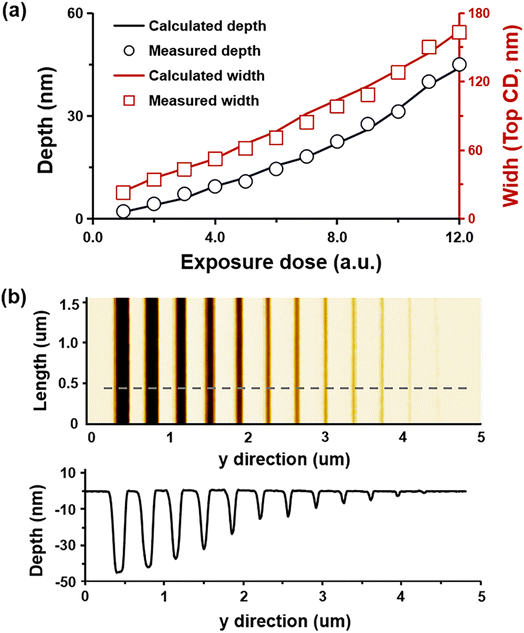 |
| | Fig. 6 Dose calibration curves of line-mapping pattern. (a) Depth and width of line-mapping patterns plotted as a function of exposure dose. Red squares and black circles are experimental data, red and black solid lines are obtained with the simulated data, respectively. (b) AFM measurement result and the cross-section profile of the line-mapping pattern as indicated by the gray line. | |
To further demonstrate that this one-step maskless plasmonic lithography is capable of fabricating micro–nano structures with arbitrary shapes, a grayscale image of Lena, which is a model picture for image processing, was used as the target image (Fig. 7a).1 The Lena pattern contains complicated micro-nano structures and the dimension span is from nanometers to several micrometers, greatly increasing the difficulty of patterning. However, the feature size manipulation mechanism makes the plasmonic lithography possible to modulate the arbitrary features of the Lena pattern according to a given grayscale exposure map. As shown in Fig. 8a, when a Lena image with arbitrary shapes needs to be fabricated, the required spatial distribution is first converted into the grayscale exposure map. Then, when the exposure dose of the target pattern is modulated, binary assist features are added to correct the pattern distortion caused by the decaying characteristics and asymmetrical distribution of the evanescent field in the scanning direction, as shown in Fig. 7b. As proof of concept, the patterned scalable nanostructure of Lena within a frame size of 5 × 5 μm and a peak-valley height of 50 nm with various widths is shown in Fig. 7. Fig. 7c and d show the 3D and 2D AFM images of the patterned Lena nanostructure, and the two sections of the fabricated Lena nanostructure that are indicated by the red and blue lines. From these results, we can conclude that the grayscale-patterned method can ensure a precise control of the surface profile of the nanostructure to be fabricated by using plasmonic lithography.
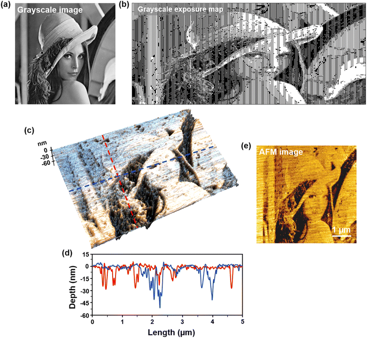 |
| | Fig. 7 A grayscale image and the corresponding experimental result. (a) The grayscale image of Lena. (b) The grayscale exposure map of Lena. (c) 3D AFM image of the fabricated Lena and (d) cross-section profiles of the fabricated Lena as indicated by the red and blue lines in (c). (e) 2D AFM topographic view of the fabricated Lena. | |
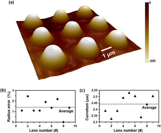 |
| | Fig. 8 Experimental results of MLA. (a) AFM measurement result of the generated MLA. (b) The calculated radius errors of the total 9 microlens shown in (a). (c) The calculated curvature of the total 9 microlens shown in (a). | |
4.2 Fabrication of microlens array (MLA) with high uniformity
As a typical 3D structure with unique optical properties, microlens array (MLA) has been widely used in many fields, such as laser beam shaping, optical imaging system, optical fiber coupling, and micro-manufacturing.47,48 In order to demonstrate the patterning results with high uniformity, MLA with curved geometry was successfully generated. The shape factors of the generated MLA were measured using AFM, and the measured results are shown in Table 1. As displayed in Fig. 8a, the generated MLA has a height of 200 nm, diameter of 1.80 μm, and radius of curvature of 2.40 μm. According to the geometry and optical theory,49 we also calculated the focal length and the NA of the MLA, which are 4.87 μm and 1.9, respectively. In order to quantitatively analyze the quality of the MLA, the radius error and the curvature of the MLA are calculated to evaluate the uniformity of the MLA, as shown in Fig. 8b and c. From the measured results as shown in Table 1 and Fig. 8, the surface roughness of the generated MLA is 11.60 nm, and uniformity of the generated MLA is 97.32%. These results indicate that high pattern uniformity can be achieved using the gray-scale patterned method in plasmonic lithography.
Table 1 Specification of the fabricated MLA
| # of lens |
1 |
2 |
3 |
4 |
5 |
6 |
7 |
8 |
9 |
Average |
| Diameter (μm) |
1.82 |
1.80 |
1.82 |
1.86 |
1.88 |
1.87 |
1.80 |
1.84 |
1.87 |
1.84 ± 0.030 |
| Curvature (μm) |
2.39 |
2.33 |
2.39 |
2.49 |
2.53 |
2.51 |
2.34 |
2.44 |
2.51 |
2.44 ± 0.077 |
| RMS surface error (nm) |
11.76 |
12.15 |
11.00 |
11.78 |
12.12 |
11.96 |
10.93 |
11.35 |
11.39 |
11.60 ± 0.456 |
| RPV surface error (nm) |
2.24 |
2.34 |
1.96 |
2.16 |
2.29 |
2.33 |
1.96 |
2.09 |
2.04 |
2.16 ± 0.152 |
| Focal length (μm) |
4.78 |
4.66 |
4.78 |
4.99 |
5.06 |
5.01 |
4.68 |
4.88 |
5.01 |
4.87 ± 0.154 |
| Numerical aperture (NA) |
0.19 |
0.19 |
0.19 |
0.19 |
0.19 |
0.19 |
0.19 |
0.19 |
0.19 |
0.19 ± 0.003 |
5 Conclusions
A maskless plasmonic lithography method to realize the rapid, cost-effective, and high-fidelity fabrication of micro–nano structures with arbitrary surface profiles is proposed. Unlike conventional optical lithography, the decaying features of plasmonic BNA show a scaling behavior, which can yield a wider bandwidth of required exposure dose per unit volume in plasmonic lithography and allow the precise manipulation of feature size for nanostructure with arbitrary shapes. A special digital grayscale exposure map is applied to spatially modulate the exposure dose according to the feature size of a given target pattern. Importantly, the dose calibration curves between exposure features and exposure variations compensate for the nonlinear effect between the intensity and the grayscale value of the exposure map, as well as the nonlinear relationship between the exposure features and dose and can be used to generate appropriate grayscale exposure map and ensure a precise control of pattern profile of the target nanostructure to be fabricated scalably. Using this method, we successfully patterned a Lena nanostructure with high relief and MLA with high uniformity. The results demonstrate that the proposed patterning strategy of compensating the nonlinear effect in plasmonic lithography caused by the rapid decaying features of the evanescent field can be directly used to control the grayscale value of the exposure map for patterning the nanostructure with arbitrary shapes. We expect that the one-step maskless plasmonic lithography can be applied to fabricate more complex nanostructures with high pattern quality and can be proven useful for many applications, especially the IC chip.
Conflicts of interest
There are no conflicts to declare.
Acknowledgements
This work is supported by the University of Chinese Academy of Sciences (Grant#118900M032) and China Fundamental Research Funds for the Central Universities (Grant# E2ET3801).
References
- X. Zhou, Z. Liu, Z. Xie, X. Liu and Z. Zheng, Small, 2012, 8, 23 Search PubMed.
- X. Wang, J. Liu, J. Han, N. Zhang, X. Li, B. Hu and Y. Wang, Opt. Express, 2014, 22, 20387–20395 CrossRef PubMed.
- J. Henzie, M. H. Lee and T. W. Odom, Nat. Nanotechnol., 2007, 2, 549–554 CrossRef CAS PubMed.
- O. Vanderpoorten, Q. Peter, P. K. Challa, U. F. Keyser, J. Baumberg, C. F. Kaminski and T. P. J. Knowles, Microsyst. Nanoeng., 2019, 5, 40 CrossRef PubMed.
- D. Yang, Z. Lei, L. Li, W. Shena, H. Li, C. Gui and Y. Song, Opt. Lasers Eng., 2023, 161, 107347 CrossRef.
- Y. Yan, Z. Hu, X. Zhao, T. Sun, S. Dong and X. Li, Small, 2010, 6, 724–728 CrossRef CAS PubMed.
- S. A. Yianni, M. Hofmann, A. K. Schenk, C. Reuter, I. W. Rangelow and C. I. Pakes, Appl. Phys. Lett., 2022, 120, 093503 CrossRef CAS.
- J. Deng, L. Jiang, B. Si, H. Zhou, J. Dong and P. Cohen, J. Manuf. Process., 2021, 66, 565–573 CrossRef.
- G. Seniutinas, A. Balčytis, I. Reklaitis, F. Chen, J. Davis, C. David and S. Juodkazis, Nanophotonics, 2017, 6, 923–941 CrossRef.
- P. Fan, J. Gao, H. Mao, Y. Geng, Y. Yan, Y. Wang, S. Goel and X. Luo, Micromachines, 2022, 13, 228 CrossRef PubMed.
- L. Huang, C. Liu, H. Zhang, S. Zhao, M. Tan, M. Liu, Z. Jia, R. Zhai and H. Liu, Opt. Laser Technol., 2023, 157, 108666 CrossRef CAS.
- C. Eschenbaum, D. Großmann, K. Dopf, S. Kettlitz, T. Bocksrocker, S. Valouch and U. Lemmer, Opt. Express, 2013, 21, 29921–29926 CrossRef PubMed.
- Z. Gan, Y. Cao, R. A. Evans and M. Gu, Nat. Commun., 2013, 4, 2061 CrossRef PubMed.
- J. Wu, C. Yu, S. Li, B. Zou, Y. Liu, X. Zhu, Y. Guo, H. Xu, W. Zhang, L. Zhang, B. Liu, D. Tian, W. Huang, M. P. Sheetz and F. Huo, Langmuir, 2015, 31, 1210–1271 CrossRef CAS PubMed.
- D. J. Glugla, M. B. Chosy, M. D. Alim, A. C. Sullivan and R. R. Mcleod, Opt. Express, 2018, 26, 1851–1868 CrossRef CAS PubMed.
- A. Grushina, Adv. Opt. Technol., 2019, 8, 163–169 CrossRef CAS.
- H. Chien, Y. Chiu and Y. Lee, Opt. Lasers Eng., 2021, 136, 106313 CrossRef.
- S. Heiskanen, Z. Geng, J. Mastomäki and I. J. Maasilta, Adv. Eng. Mater., 2020, 22, 1901290 CrossRef CAS.
- H. Yu, Q. Zhang, X. Chen, H. Luan and M. Gu, Adv. Photon., 2022, 4, 034002–034013 CAS.
- T. Cao, M. Lian, X. Chen, L. Mao, K. Liu, J. Jia, Y. Su, H. Ren, S. Zhang, Y. Xu, J. Chen, Z. Tian and D. Guo, OES, 2022, 1, 210010 CAS.
- Z. Lin, L. Ji and M. Hong, Nano Lett., 2022, 22, 7005–7010 CrossRef CAS PubMed.
- M. Cen, J. Wang, J. Liu, H. He, K. Li, W. Cai, T. Cao and Y. Liu, Adv. Mater., 2022, 34, 2203956 CrossRef CAS PubMed.
- V. Grigaliūnas, A. Lazauskas, D. Jucius, D. Viržonis, B. Abakevičienė, S. Smetona and S. Tamulevičius, Microelectron. Eng., 2016, 164, 23–29 CrossRef.
- M. Erdmanis and I. Tittonen, Appl. Phys. Lett., 2014, 104(073118), 1–5 Search PubMed.
- G. Kumar, H. Tang and J. Schroers, Nature, 2009, 457, 868–872 CrossRef CAS PubMed.
- L. Guo, Adv. Mater., 2007, 19, 495–513 CrossRef CAS.
- H. Solak, C. David, J. Gobrecht, V. Golovkina, F. Cerrina, S. Kim and P. Nealey, Microelectron. Eng., 2003, 67–68, 56–62 CrossRef CAS.
- D. Xia, Z. Ku, S. Lee and S. Brueck, Adv. Mater., 2011, 23, 147–179 CrossRef CAS PubMed.
- S. Kim, H. Jung, Y. Kim, J. Jang and J. W. Hahn, Adv. Mater., 2012, 24, 337–344 Search PubMed.
- W. Lee, T. Kim, G. Choi, G. Lim, H. Joe, M. Gang, H. Moon, D. Kim, B. Min, Y. Park and N. Park, Appl. Phys. Lett., 2015, 106, 051111–051115 CrossRef.
- F. Hong and R. Blaikie, Adv. Opt. Mater., 2019, 7, 1801653 CrossRef.
- D. Han, S. Deng, T. Ye and Y. We, Microsyst. Nanoeng., 2023, 9, 1–13 CrossRef PubMed.
- H. Jung, C. Park, S. Oh and J. W. Hahn, Sci. Rep., 2017, 7, 9721 CrossRef PubMed.
- S. Oh, D. Han, H. Shim and J. W. Hahn, Nanotechnology, 2018, 29, 045301 CrossRef PubMed.
- D. Han and Y. Wei, Opt. Express, 2022, 30, 20589–20604 CrossRef CAS PubMed.
- C. Guo, S. Cao, P. Jiang, Y. Fang, J. Zhang, Y. Fan, Y. Wang, W. Xu, Z. Zhao and Q. Liu, Opt. Express, 2009, 7, 19981–19987 CrossRef PubMed.
- Y. Pang, Y. Shu, M. Shavezipur, X. Wang, M. Mohammad, Y. Yang, H. Zhao, N. Deng, R. Maboudian and T. Ren, Sci. Rep., 2016, 6, 28552 CrossRef PubMed.
- Y. Chen, J. Gao and X. Yang, Adv. Opt. Mater., 2019, 7, 1801467 CrossRef.
- Z. Gan, H. Feng, L. Chen, S. Min, C. Liang, M. Xu, Z. Jiang, Z. Sun, C. Sun, D. Cui and W. Li, Light: Sci. Appl., 2022, 11, 1–10 CrossRef PubMed.
- D. Han, C. Park, S. Oh, H. Jung and J. W. Hahn, Nanophotonics, 2019, 8, 879–888 CrossRef.
- D. Amarie, N. D. Rawlinson, W. L. Schaich, B. Dragnea and S. C. Jacobson, Nano Lett., 2005, 5, 1227–1230 CrossRef CAS PubMed.
- P. Gao, N. Yao, C. Wang, Z. Zhao, Y. Luo, Y. Wang, G. Gao, K. Liu, C. Zhao and X. Luo, Appl. Phys. Lett., 2015, 106, 1–6 Search PubMed.
- Y. Hu and Y. Meng, Friction, 2018, 6, 443–456 CrossRef.
- Y. Kim, H. Jung, S. Kim, J. Jang, J. Y. Lee and J. W. Hahn, Opt. Express, 2011, 19, 19296–19309 CrossRef CAS PubMed.
- C. Wang, P. Gao, Z. Zhao, N. Yao, Y. Wang, L. Liu, K. Liu and X. Luo, Opt. Express, 2013, 21, 20683–20691 CrossRef PubMed.
-
S. Kim, PhD thesis, Yonsei Univeristy, Seoul, Korea, 2014.
- H. Zhang, L. Li, D. L. McCray, S. Scheiding, N. J. Naples, A. Gebhardt, S. Risse, R. Eberhardt, A. T. nnermann and A. Y. Yi, Opt. Express, 2013, 21, 22232–22245 CrossRef PubMed.
- M. Elsherif, R. Moreddu, M. U. Hassan, A. K. Yetisen and H. Butt, Lab Chip, 2019, 19, 2060–2070 RSC.
- P. Nussbaum, R. Völkel, H. P. Herzig, M. Eisner and S. Haselbeck, Pure Appl. Opt., 1997, 6, 617–636 CrossRef.
|
| This journal is © The Royal Society of Chemistry 2023 |
Click here to see how this site uses Cookies. View our privacy policy here. 
 Open Access Article
 This Open Access Article is licensed under a Creative Commons Attribution-Non Commercial 3.0 Unported Licence
 a,
Tianchun
Ye
*ab and
Yayi
Wei
*ab
a,
Tianchun
Ye
*ab and
Yayi
Wei
*ab