
 Open Access Article
 This Open Access Article is licensed under a Creative Commons Attribution-Non Commercial 3.0 Unported Licence
Local phonon imaging of AlN nanostructures with nanoscale spatial resolution
Ilya
Milekhin
 *abcd,
Kirill
Anikin
c,
Nina N.
Kurus
c,
Vladimir G.
Mansurov
c,
Timur V.
Malin
c,
Konstantin S.
Zhuravlev
c,
Alexander G.
Milekhin
cd,
Alexander V.
Latyshev
cd and
Dietrich R. T.
Zahn
ab
*abcd,
Kirill
Anikin
c,
Nina N.
Kurus
c,
Vladimir G.
Mansurov
c,
Timur V.
Malin
c,
Konstantin S.
Zhuravlev
c,
Alexander G.
Milekhin
cd,
Alexander V.
Latyshev
cd and
Dietrich R. T.
Zahn
ab
aSemiconductor Physics, Chemnitz University of Technology, D-09107 Chemnitz, Germany
bCenter for Materials, Architectures, and Integration of Nanomembranes (MAIN), Chemnitz University of Technology, Chemnitz, Germany
cA.V. Rzhanov Institute of Semiconductor Physics, pr. Lavrentieva, 13, 630090, Novosibirsk, Russia
dNovosibirsk State University, Pirogov, 1, 630090 Novosibirsk, Russia. E-mail: mia2994@gmail.com
First published on 21st April 2023
Abstract
We demonstrate local phonon analysis of single AlN nanocrystals by two complementary imaging spectroscopic techniques: tip-enhanced Raman scattering (TERS) and nano-Fourier transform infrared (nano-FTIR) spectroscopy. Strong surface optical (SO) phonon modes appear in the TERS spectra with their intensities revealing a weak polarization dependence. The local electric field enhancement stemming from the plasmon mode of the TERS tip modifies the phonon response of the sample, making the SO mode dominate over other phonon modes. The TERS imaging allows the spatial localization of the SO mode to be visualized. We were able to probe the angle anisotropy on the SO phonon modes in AlN nanocrystals with nanoscale spatial resolution. The excitation geometry and the local nanostructure surface profile determine the frequency position of SO modes in nano-FTIR spectra. An analytical calculation explains the behaviour of SO mode frequencies vs. tip position with respect to the sample.
1 Introduction
The local spectral analysis of nanostructures attracts growing attention because of the trend in the miniaturization of active elements in modern electronics, chemistry, medicine, and biology.1–3 Among a wide variety of analytical methods, vibrational spectroscopy stands out as a non-destructive and highly sensitive method for probing minute variations of sample parameters. Widely used vibrational spectroscopy techniques like FTIR absorption/reflection/scattering and Raman scattering provide access to a broad range of nanostructure properties (size, elemental composition, mechanical stress, etc.). However, optical methods are restricted in spatial resolution by the Abbe diffraction limit. In the last few decades, the popularity of scanning probe techniques, like atomic force and scanning tunneling microscopies (AFM and STM), grew exponentially, thanks to their ability to analyse the surface properties of the materials with nanoscale spatial resolution. However, these probe methods provide limited access to the chemical sample properties. These reasons lead to a growing interest in combining spectroscopy and scanning probe methods like FTIR or Raman scattering with AFM leading to nano-FTIR and TERS allowing phonon spectra to be recorded with a spatial resolution of several nanometres.4–14It is worth mentioning that the complementary analysis of the same sample using both TERS and nano-FTIR spectroscopies may bring the following advantages:
(i) in the case of a multicomponent sample, the different phases could be more effectively identified due to the different phonon selection rules of the two methods,
(ii) different excitation mechanisms of TERS and nano-FTIR can lead to enhancement of the different phonon modes, thus providing more detailed information on the phonon spectrum of a nanostructure,
(iii) TERS and nano-FTIR absorption are methods with different orders of light interaction with matter allowing deeper physical insight into the processes of photon, electron, and phonon coupling.
Group III nitrides like AlN, GaN, InN, and BN, and their alloys are highly promising materials for modern electronics thanks to their widely varied and direct (in the case of wurtzite crystal structure) bandgap, high luminescence efficiency, excellent electron transport properties, thermal stability, and large piezoelectric constants.15 Moreover, quantum wells, modulation-doped heterointerfaces, and heterojunction structures based on these materials can be fabricated with further improved properties.16,17 Consequently, group III nitride-based nanostructures have become interesting candidates for spectral analysis with nanometre-scale spatial resolution. The ability to measure edge effects at heterojunctions, to probe optical properties of single nanostructures, and to study contact effects is of crucial importance for nitride-based electronic devices.
Raman scattering by bulk nitrides is relatively well discussed and understood,18,19 while Raman spectra of nitride nanostructures like nanowires, nanodots, etc. are much less studied. There are several papers devoted to the analysis of Raman scattering in nanorod-like nitrides nanostructures.20–24 As well as for the Raman scattering from bulk nitrides, Raman spectra of the above-mentioned nanostructures demonstrate polarization-dependent selection rules: wherever excitation is oriented along or perpendicular to the c-axis of the nanostructure. As a rule, similar to bulk nitrides mainly E2, A1, and E1 modes for AlN nanorods were detected. In addition to the bulk-related phonon modes, some authors were able to detect surface optical (SO) phonon modes. The absence or appearance of the SO modes in Raman spectra can be probably explained by a difference in the shape of the nanostructures investigated in different groups. The variation of excitation polarisation analysis reveals the dependency of SO mode spectral position on the excitation wavevector with respect to the c-axis of the nanostructure. Such dependency originated from the influence of the nanorod edges on SO mode formation. The authors of (ref. 20) and (ref. 23) demonstrate the dependency of the SO mode on nanotip or nanorod diameter that as well supports such an explanation. The strong optical anisotropy and the polar nature of nitride nanorods induce the splitting of the SO mode into two peaks.23
In comparison with micro-Raman spectroscopy, which provides information averaged over the area illuminated by the focused laser beam, i.e. a typical area in the μm2-range, the strong plasmonic enhancement of the incident electric field near the apex of a metallic AFM tip improves the lateral resolution to values comparable with the tip size or below so that TERS spectra can provide detailed information on the phonon spectrum of a single nanostructure. Early TERS measurements were performed for GaN thin films25 and nanowires26 using an inverted confocal microscope, and single far- and near-field Raman spectra were compared. In ref. 25, the crystalline properties of a 500 nm-thick GaN film grown on a c-plane sapphire substrate were analysed utilizing silver-coated AFM tips illuminated with an excitation wavelength of 532 nm. The most pronounced TERS enhancement was observed for the E1(TO) mode, with some increase in intensity for A1(TO) and E1(LO) modes. The appearance of the A1(TO) and E1(TO) modes is explained by the influence of the metal TERS tip, which induces a strong electric field enhancement near the tip apex close to the sample surface. The E1(LO) mode, because of the Raman selection rules, is prohibited in backscattering geometry from a c-axis oriented hexagonal crystal, like GaN.27 However, this mode is activated in TERS experiments. According to (ref. 25) an observation of this mode is explained by the secondary interaction of the TERS tip with the scattered Raman signal excited by the incident laser light. The polarization of the scattered signal for the E1(LO) mode can be oriented in the z-direction; hence coupling with the tip produces a secondary enhanced E1(LO) mode oriented in the z-direction. The appearance of the A1(LO) mode is explained by a large solid angle of the objective lens of the Raman microscope (the so-called leakage effect).18 Unlike far-field micro-Raman measurements, the E2(high) mode is absent in the near-field spectra while it does not possess a dipole moment.
For TERS experiments with a single gallium nitride (GaN) nanowire,26 silver- and gold-coated tips and excitation wavelengths of 514 and 647 nm, respectively, were utilized. A selective enhancement of the E1(TO) mode in the TERS spectra was observed, while the E2 mode was also absent in the TERS spectra. TERS implies that selection rules in crystalline structures are changed in the presence of a strong electric field and that new modes usually forbidden in conventional Raman spectra can be observed at the nanoscale due to the polarisation of the tip-induced field.28 Broken Raman selection rules explain the appearance of “prohibited” modes at the field gradient near the curved nanoobject surfaces. Meanwhile, in (ref. 29) the authors demonstrate the independence of TERS intensities from the polarisation of incident light. However, TERS experiments with different polarization, excitation wavelength, and tip material, especially, for probing anisotropic uniaxial nanostructures are still quite rear, and understanding of TERS by phonon modes requires substantial efforts.
The Dhara group carried out several TERS studies aimed at probing the phonon spectra of single GaN nanowires with diameters of approximately 40–80 (ref. 30) and 200 nm.31 The authors used a bent glass tip with an embedded Au nanoparticle of 100 nm diameter at the end of the tip and an excitation wavelength of 514 nm. In ref. 30, TERS spectra measured in the backscattering geometry reveal pronounced A1(LO) and A1(TO) modes, as well as the SO mode is associated with a breaking symmetry at the surface of the nanowire. The asymmetry of the LO mode observed in the presence of doping was explained by phonon-free carrier interaction. In contrast, in ref. 31, A1(TO), E1(TO), and E2(high) modes are observed, while hardly any contribution of A1(LO) and SO modes can be seen in the TERS spectra despite similar experimental conditions. Moreover, the authors of ref. 31 use different metal substrates in order to increase the TERS intensity in the so-called gap-mode TERS condition, but the gap-mode effect was not realised due to the large sample thickness (200 nm). In ref. 31, an Al substrate was chosen, which minimized the losses in scattered radiation and enhanced the collection efficiency of the TERS signal during the imaging.
In ref. 32, the authors investigated InN surfaces utilizing a 633 nm excitation laser and gold TERS tips fabricated using electrochemical etching. They observed near-field A1(TO) Raman modes, not detectable in the far-field spectra. In addition, new modes at frequencies above that of the A1(TO) mode were detected and assigned to second-order combinational modes consisting of optical zone-center phonons and acoustic phonons from the edge of the Brillouin zone.
In ref. 33, the TERS efficiency (EFAlN) was estimated for the A1(TO) mode in AlN nanocones with variable diameters from 200 to 600 nm under 514.5 nm excitation using a bent glass tip with an Au nanoparticle (diameter <100 nm) at the end. The values of EFAlN were found to be in the range of ∼30 to 74. The A1(TO) mode was the only mode observed in the measurements; meanwhile, SO modes did not appear in the TERS spectra. Note that the selective enhancement of the SO phonon modes in AlN, GaN, and ZnO nanostructures after the vacuum deposition of silver on top of the sample was previously observed by our group using surface-enhanced Raman scattering (SERS)34 and should be also allowed in TERS spectra. Upon Ag deposition, the intensity of the SO mode can dominate in the SERS spectra, while the E2(high) and A1 modes remain nearly unchanged.34
The authors of ref. 35 studied TERS by optical phonons in GaN-based nanorods with InGaN/GaN multi-quantum wells using a 632.8 nm excitation wavelength and a gold TERS tip. In this case, they observed enhanced SO modes from GaN layers not detected in far-field measurements.
The results presented in the literature mentioned above are summarized in Table 1, along with TERS, SERS, and micro-Raman measurements discussed in this work.
| Excitation, nm | Material | Tip type | A1(TO)/A1(LO) | E1(TO)/E1(LO) | SO | E2(high) | Ref. |
|---|---|---|---|---|---|---|---|
| 514 | Single GaN nanowire | —, (micro Raman) | ***/* | — | — | — | 41 |
| 514 | Single GaN nanowire | Si/Ag and Si/Au | */— | — | — | — | 26 |
| 514 | Single GaN nanowires diameter 40–80 nm | Glass/Au particle (diameter <100 nm) | ***/*** | −/− | ** | *** | 30 |
| 514 | Single GaN nanowires diameter 200 nm | Glass/Au nanoparticle (diameter 100 nm) | ***/* | ***/* | — | *** | 31 |
| 514 | AlN tips (with variable diameter from 200 to 600 nm) | Glass/Au nanoparticle (diameter <100 nm) | ***/— | — | — | — | 33 |
| 532 | GaN film | Si/Ag | */* | ***/** | * | — | 25 |
| 532 | AlN nanowire | —, (micro Raman) | **/** | −/− | — | *** | This study |
| 633 | InN film | Au tip | ***/*** | −/− | — | — | 32 |
| 633 | GaN-based nanorods with InGaN/GaN multi-quantum wells | Au tip | **/** | ***/*** | ** | — | 35 |
| 638 | AlN nanowire | —, (micro Raman) | */* | −/− | — | ** | This study |
| 638 | AlN nanowire | Si/Au | −/− | −/− | *** | ** | This study |
| 647 | Single GaN nanowire | Si/Ag and Si/Au | */— | — | — | — | 26 |
| 785 | AlN thin film | —, (micro Raman) | */* | −/− | — | ** | This study |
Such strong differences in the reported observation of phonon modes, including selective TERS enhancement of modes with different symmetries, reported by several groups, appearance or complete absence of SO modes in TERS experiments, demonstrate the lack of common understanding of the mechanisms of TERS enhancement. It can be explained by the wide variation of experimental conditions, unreproducible TERS tips, as well as different coupling of the plasmon with the sample (tip-sample distance, excitation energy, type, material, and size of TERS tips, localised surface plasmon resonance energy of the tips, etc.).
The measurements of nano-FTIR absorption provide an independent view of the phonon modes of matter. At the same time, experimental studies of phonons in single nitride nanostructures (as well as in single nanostructures in general) using nano-FTIR spectroscopy are still very scarce.
The nano-FTIR analysis of SiC36,37 and GaN38 thin layers provided evidence for a local variation of the dielectric function of the sample and allowed the determination of local mechanical strain at the nanometer scale by excitation of a near-field phonon resonance. In ref. 39, the shift of the LO phonon mode due to the plasmon-phonon interaction is reported while mapping doped SiC polytypes with 20 nm spatial resolution. Very recently, we showed an analysis of optical phonon modes revealing that nano-FTIR spectroscopy can be effectively applied to determine the composition in SiO2 nanowires with a spatial resolution much below the diffraction limit.40
Complementary TERS and nano-FTIR studies are beneficial for local spectral analysis of nanoobjects, which allows detailed information on their phonon spectra to be derived. To the best of our knowledge, there is no research performed so far where both methods were used for studying the same sample. The reason for this is not only restricted access to both experimental techniques but also specific requirements for the nanoobjects, including the activity of phonon modes in both Raman and IR spectra and the phonon frequencies exceeding the cutoff frequency (near 600 cm−1) of the HgCdTe detector used in typical nano-FTIR measurements.
In this work, we probe the phonon response from single hexagonal AlN nanocrystals, which satisfy the above-mentioned requirements of the two imaging methods, nano-FTIR, and TERS spectroscopies. Employing TERS, we observed the SO modes spatially localized in different areas of AlN nanostructures, while nano-FTIR spectroscopy provides additional information on the SO phonon dispersion.
2 Experimental methods
2.1 Sample fabrication
The AlN nanostructures were grown on Si(111) substrates by means of an ultrahigh vacuum-based molecular beam epitaxy Riber CBE-32P system. A modified Shiraki chemical treatment of the Si(111) surface as described in ref. 42 was used to prepare the substrate for growth. The preparation of a clean silicon surface in an ultrahigh vacuum prior to growth was carried out in two stages. First, the Si(111) substrate was annealed at 500 °C in a preparation chamber for 2 h (background pressure ≤5 × 10⁻⁹ Tor). Then, the silicon substrate was annealed in the growth chamber at 1200 °C for 10 min. The nitridation of the Si(111) substrate was carried out by the exposure of the silicon surface to an ammonia flux of 10 sccm and 6 s exposure time with accurate control of the surface temperature equal to 1000 °C. Our previous works describe the nitridation procedure in more detail.43,44 In the next step, metallic Al was deposited on top of the (8 × 8) structure under vacuum conditions at T = 1000 °C, resulting in a (4 × 4) superstructure formation. This superstructure is related to the formation of a graphene-like AlN (g-AlN) layer with monolayer thickness. Following the growth of the AlN nucleation layer there is a 2D-3D surface morphology transition with an AlN crystal structure transformation to the wurtzite phase (w-AlN). Afterwards, the AlN thin layer was deposited at 940 °C under 60 sccm of ammonia flux, and, finally, an 1100 nm thick AlN layer was grown. The AFM images show hexagonal surface islands with a characteristic height of ∼30 nm (20–50 nm) and an average lateral size of about 250 nm, varying in the range of 200–300 nm. By etching a part of the sample in KOH solution, it was confirmed that the hexagonal islands are connected with AlN inversion domains because the islands were converted into pits by the etching.The investigated sample thus consisted of a Si substrate with a 1 μm-thick AlN crystalline layer with randomly distributed hexagonal nanocrystals. Single AlN hexagonal nanocrystals with a height of 40 nm and diameter of 280 nm were chosen for TERS and nano-FTIR measurements. Note that nanocrystals have a wurtzite crystal structure with the crystallographic c-axis perpendicular to the surface.
2.2 Raman scattering measurements
Micro-Raman measurements were carried out using an XploRA PLUS Raman spectrometer, equipped with an optical confocal microscope with 100× objective. Raman spectra were recorded in backscattering geometry with a laser excitation wavelength of 638 nm and an acquisition time of 20 s. The lateral resolution was around 1 μm, and the spectral resolution was about 1.4 cm−1 for the 2400 gr mm−1 grating. The measurements were performed in both parallel and crossed geometries. The excitation power was 2.8 mW on the sample.TERS measurements were performed using a NanoRaman Platform (HORIBA Scientific) consisting of an atomic force microscope (SmartSPM) attached to the same XploRA PLUS Raman spectrometer in side illumination/collection geometry. The angle of incidence for the laser beam is 65° relative to the surface normal. Therefore, the laser spot has an ellipsoidal shape with a size of around 1.7 μm2. The p-polarized monochromatic laser light with 638.2 nm wavelength is focused onto an inclined gold tip apex. The sample illumination and scattered light detection are performed through a long working distance objective, 100×, 0.7 NA. The TERS spectra were measured in parallel and crossed geometries: excitation light with polarisation parallel (p-polarized) or orthogonal (s-polarized) to normal of the substrate surface, respectively, while for both cases, p-polarized scattered light is detected.
TERS experiments were performed using homemade silver TERS tips with a radius of about 50 nm, as reported earlier.45 The spectral acquisition time for one TERS spectrum is 0.5 s. A 600 l mm−1 grating disperses the Raman signals and detects the photons by an electron-multiplying charge-coupled detector (EMCCD). This gives a spectral resolution of about 7.6 cm−1. For TERS mapping, the selected scanning area was chosen as 400 × 400 nm2 and 60 by 60 points.
2.3 NeaSNOM platform for Nano-FTIR spectroscopy
A NeaSNOM setup from Neaspec GmbH was used for the nano-FTIR measurements. The NeaSNOM microscope platform includes an AFM microscope and an optical system for focusing the IR light onto the metallized AFM tip. The excitation light of the broadband infrared laser covers the spectral range from 600 to 2100 cm−1. Radiation is focused onto a metal (PtIr5) tip of the AFM microscope by a parabolic mirror. The backscattered light from the metal tip passes a Michelson interferometer with the reference oscillating mirror. The nano-FTIR system allows measuring spectra with a spectral resolution of 6 cm−1. The signal is detected by a cooled mercury cadmium telluride detector (600–8000 cm−1). The typical frequency of the tip oscillation Ω is in the range of 240–380 kHz with an amplitude of around 80 nm. This device is an s-SNOM-type instrument utilizing heterodyne detection, allowing filtering out the far-field signal and extracting only the near-field nano-FTIR response.46 The detector signal is demodulated at the higher harmonics nΩ of the tip oscillation Ω and recorded as a function of the mirror position to create an interferogram ηn(ω) of nth order.47 In our nano-FTIR experiment, the order of demodulation was taken to be n = 2 to secure sufficient intensity of the near-field nano-FTIR signal.3 Results and discussion
3.1 Polarized TERS mapping of an AlN nanocrystal
Fig. 1 shows an AFM image of a single AlN nanocrystal measured with a Si commercial AFM tip with a radius of 10 nm using the XploRA TERS setup. The nanocrystal has a hexagonal shape indicating its wurtzite crystal structure, a height of about 40 nm, and a diameter of the circumscribed (inscribed) circle of about 290 (260) nm. As shown in Fig. 1, the surface of the AlN layer and the top nanocrystal surface are relatively flat (roughness of about 5 nm).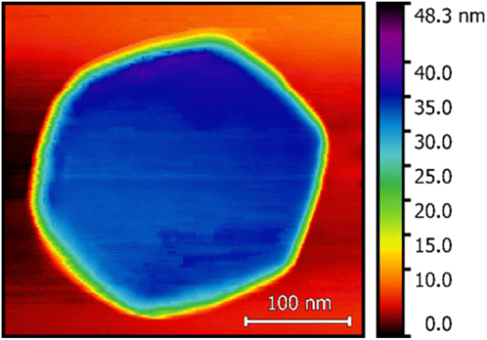 | ||
| Fig. 1 AFM image of a single hexagonal AlN nanocrystal obtained using the XploRA TERS setup. | ||
Micro-Raman spectra measured for the area with the AlN nanocrystal in backscattering geometry with 638 nm excitation wavelength for parallel and crossed geometries are presented in Fig. 2. The spectra reveal an intensive feature at 650 cm−1 attributed to the E2 (high) mode, as well as a moderate feature at 884 cm−1 assigned to the A1(LO) mode. The modes at 617, 670, and 912 cm−1 are observed in all Raman spectra with different intensities and can be attributed to the contributions of both AlN and Si phonons. The weaker line at 825 cm−1 was assigned to the Si substrate based on the measurements of a bare Si wafer using the same experimental setup and conditions. The recorded modes of the Si substrate are labeled by asterisks in Fig. 2. The frequency positions of AlN-related modes are in good agreement with literature data:19 611, 657, and 670 cm−1 for A1(TO), E2 (high), and E1(TO), and 890 and 912 cm−1 for A1(LO) and E1(LO), respectively. The broad feature near 940–1000 cm−1 is due to second-order scattering from the Si substrate. Several weaker modes indicated in Fig. 2 by asterisks refer also to multiphonon modes from Si.48 The E1(TO) mode vanishes in the experimental spectra due to Raman selection rules, which prohibit this mode in backscattering geometry while exciting along the c-axis in both parallel and crossed geometries.49 Note that SO phonon modes expected in the spectral range of the Reststrahlen band of AlN (∼600–900 cm−1) are not detectable in the micro-Raman spectra. In the micro-Raman measurements, the total film thickness is probed, while in the TERS experiment, the near-field Raman signal is analyzed, which comes from the vicinity of the TERS tip only. Therefore, optical phonons of bulk materials predominantly contribute to the conventional micro-Raman spectra. The Raman tensor of bulk hexagonal AlN crystal was analyzed in ref. 49. The wurtzite AlN structure belongs to the space group C6V; according to group theory, one A1, one E1, and two E2 modes are Raman active,27 where A1 is polarized along the c-axis, while E1 is polarized in the orthogonal plane.
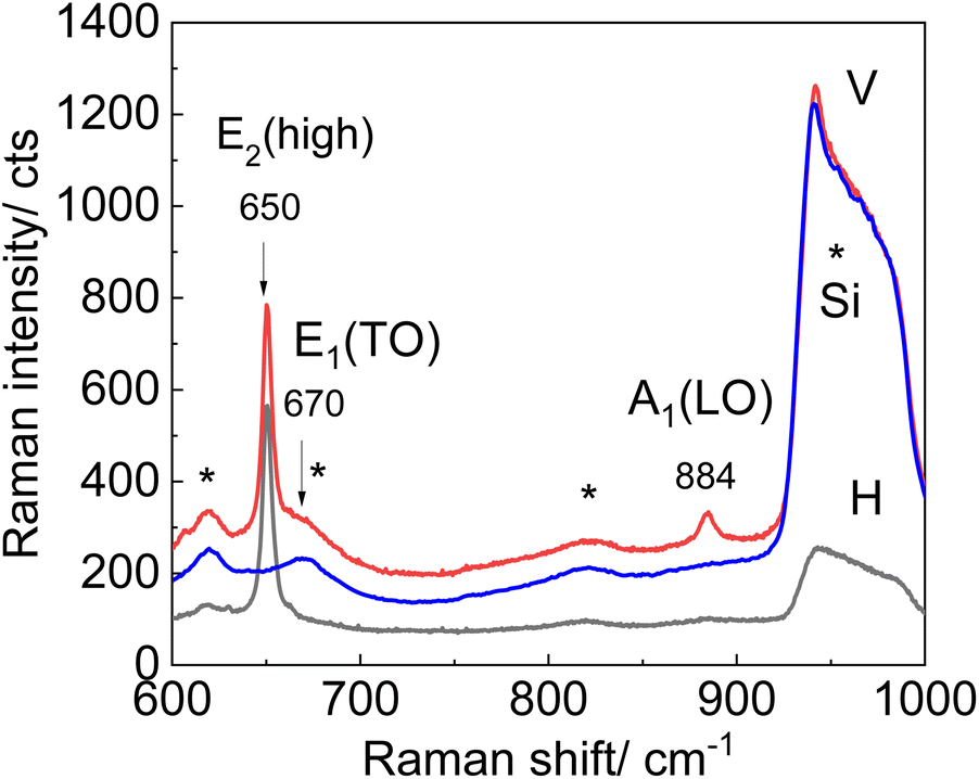 | ||
| Fig. 2 Micro-Raman spectra of hexagonal AlN nanocrystals obtained using XploRA setup for parallel (red) and crossed polarized (black) backscattering geometries. The Raman spectrum of a bare Si(111) substrate measured for parallel scattering geometry is shown for comparison (blue). Asterisks indicate multiphonon modes from Si. The intensity of Raman scattering from a Si substrate is normalized to a maximum at 950 cm−1 for better visibility of weak peaks. | ||
TERS spectra for parallel and crossed geometries with TERS tip positioned on the surface of the AlN layer outside of the AlN nanocrystal and on the nanocrystal are shown in Fig. 3a and b, respectively. Besides vibrational modes around 300, 520, and 950 cm−1, which were attributed to the first and second Raman scattering from the Si substrate (2 TA, LO, and 2TO, respectively),50 the feature at 650 cm−1 is assigned as the E2(high) phonon mode in the AlN film and crystal. TERS spectra reveal a broad asymmetric feature in the range of 600–900 cm−1, which can be decomposed in two modes near 730 and 790 cm−1. The possibility to decompose SO mode into two components which originate from optical phonons of the A1 and E1 symmetries (A and S modes as shown in Fig. 3) was addressed earlier.23,24,34 Note, that the intensity of TERS by SO modes from the area outside of the AlN nanocrystal is weaker than that from the nanocrystal for both polarisations. Usually, SO modes cannot be observed in optical experiments due to momentum conservation constraints. Activation of the surface modes becomes possible only if a source of wave vector is supplied through strong Fourier components of the surface potential.51 This can be accomplished, e.g. by surface roughness, or by the construction of a grating along the surface providing phonon momentum along the sample surface. Both these conditions are fulfilled in our TERS experiment. The surface roughness determined from AFM measurements is about 5 nm, while the TERS tip serves as a source of the radiation scattered partially along the sample surface.
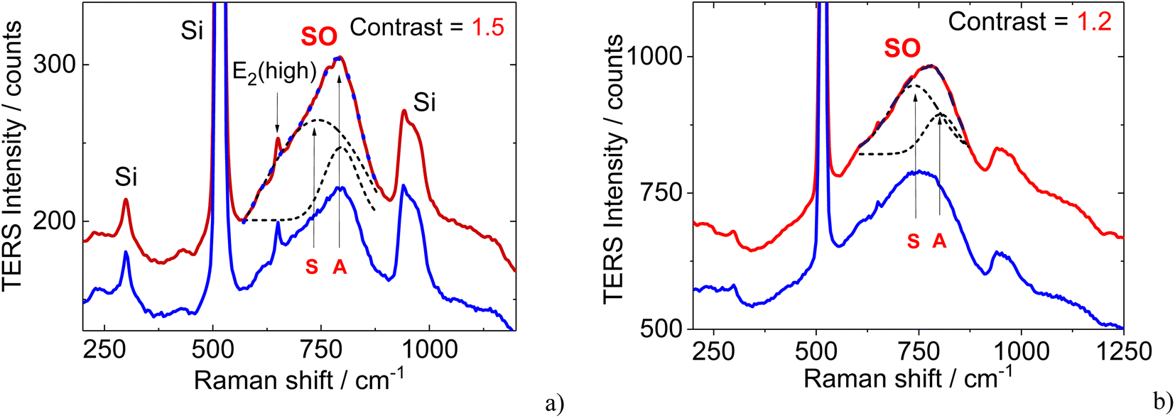 | ||
| Fig. 3 TERS spectra of a single AlN nanocrystal measured with (a) parallel and (b) crossed geometries excited with 638.2 nm. The red and blue spectra show the averaged spectra from the area on the AlN nanocrystal and outside of the nanocrystal, respectively, averaged over the boxes as indicated in Fig. 4. The dashed lines show deconvolution of the experimental spectra by two Gaussians. Symmetrical and asymmetrical SO modes in AlN originated from optical phonons with A1 and E1 symmetries are indicated as (S and A) modes. The background is subtracted in all spectra. | ||
The intensity of these modes observed from the AlN nanocrystal exceeds that from the AlN layer by a factor of about 1.5 (1.2) for vertical (horizontal) polarization. Note that here this factor is a contrast which compares TERS mode intensities when the tip is in direct contact with the sample surface (contact mode). Typically, in the literature TERS enhancement factor is defined as a ratio 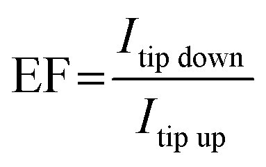 where Itip down is the TERS intensity in the contact mode and Itip up is the Raman intensity when the tip is lifted up to the distance of about 50 nm.52 However, in this case, determination of the TERS enhancement factor using a tip-up/down approach requires averaging over a significant number of measurements because the Raman spectra are very much site dependent resulting in a wide spread of enhancement coefficients. Therefore, here the contrast was used for visualization of single nanocrystals which was calculated as an average of 81 TERS spectra on AlN nanocrystal and on the AlN layer (see Fig. 4, blue and red squares).
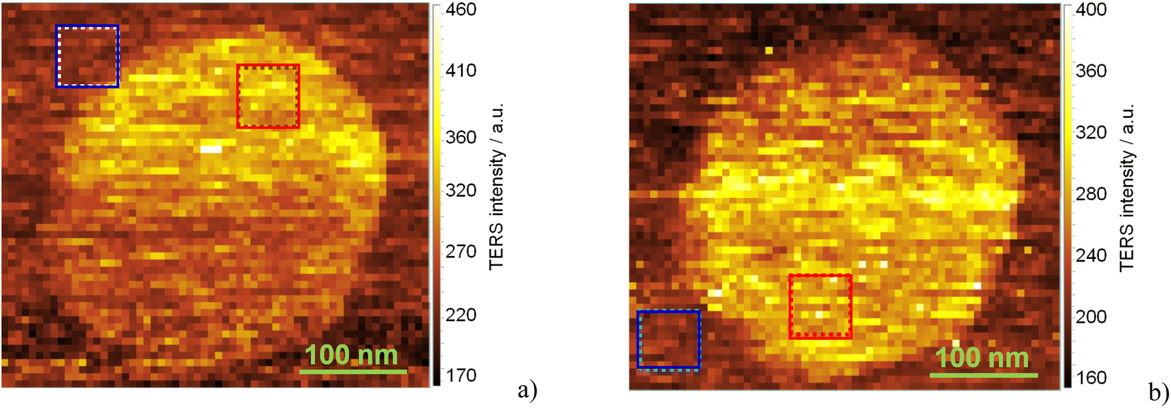 | ||
| Fig. 4 TERS maps of Raman intensity in the spectral range of SO phonons (570–900 cm−1) derived from TERS spectra of a single AlN nanocrystal measured in (a) parallel and (b) crossed geometry. The red and blue dotted squares show the regions on and outside the AlN nanocrystal, for which the TERS spectra were averaged. The averaged TERS spectra on and outside the nanocrystal for parallel and crossed polarization are shown in Fig. 3a and b, respectively. TERS maps represent the combination of near- and far-field signals. The step size of the TERS maps is about 7 nm. | ||
The noticeable contrast in the Raman scattering intensities of SO modes from the nanocrystal and the AlN layer can occur due to a higher surface-area-to-volume ratio for the AlN nanocrystals with respect to that for the flat AlN layer. However, the size of the AlN nanocrystal exceeds only twice that of the TERS tip; therefore, the influence of nanocrystal geometry and its edges become noticeable.
We performed TERS mapping of the SO mode spectral region (600–900 cm−1) for two different polarizations. Fig. 4a and b shows TERS images of the AlN nanocrystal recorded for parallel and crossed geometries, respectively. TERS images of an AlN nanocrystal, which reveal its hexagonal shape, are similar to the AFM image of the same nanocrystal. As a rule, the parallel geometry (light polarized along the TERS tip) is used in the majority of TERS experiments, as this geometry provides maximal TERS enhancement.53 But in our experiments we did not observe a dramatic difference between both experimental geometries, that stay in correlation with conclusions made by authors,29 their TERS intensities largely independent from excitation polarization. The authors of ref. 29 developed the quantum mechanics approach, where the scattering process is mediated by the formation of plasmon-polariton (PP) at the metal tip; PP is presumably polarized along the tip, independently of excitation photon polarization.
3.2 Nano-FTIR spectroscopy of a single AlN nanocrystal
Fig. 5 shows a typical AFM image of the same AlN nanocrystal (as shown in Fig. 1) measured using a nano-FTIR setup with a Pt–Ir tip. The nano-FTIR amplitude spectra representing 2nd-order of demodulated near-field amplitudes a2(ω) as defined in40 were measured across the AlN nanocrystal along the red and blue lines as marked in Fig. 5. For the red (blue) line with a length of 500 (200) nm the nano-FTIR spectra were measured with a step of 10 (5) nm.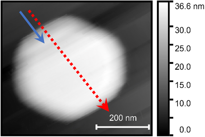 | ||
| Fig. 5 AFM image of the same single hexagonal AlN nanocrystal as shown in Fig. 1 but measured using a nano-FTIR setup. The dashed red (solid blue) arrow shows the direction, and scanning range of the 500 (200) nm long nano-FTIR profiles with 10 (5) nm step size. | ||
Contrary to TERS spectra, the nano-FTIR measurements demonstrate pronounced changes in the positions of the phonon features as a function of tip position on the sample surface. Fig. 6a displays the changes in the mode frequencies across the whole AlN as shown in Fig. 5 by a red arrow. Note, that these changes are almost symmetrical with respect to the nanocrystal center. Fig. 6b displays in detail the most pronounced changes in the mode frequencies occurring at the nanocrystal edge along the blue scan line as shown in Fig. 5.
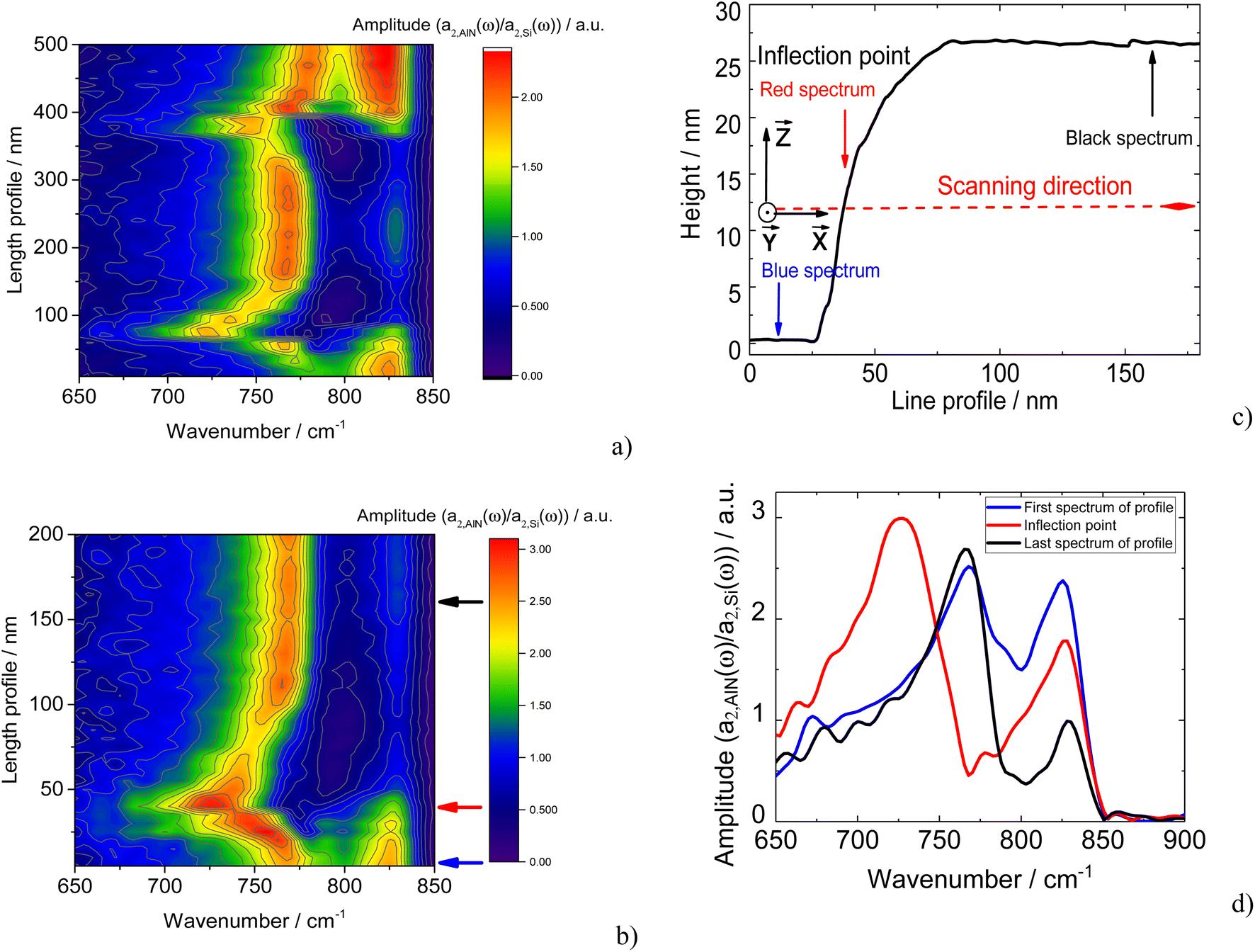 | ||
| Fig. 6 (a) 50 nano-FTIR spectra measured along the 500 nm line with a step of 10 nm (red line in Fig. 5). (b) 40 nano-FTIR spectra measured along the 200 nm line with a step of 5 nm (blue line in Fig. 5). (c) The AFM profile of the AlN nanocrystal along the blue line in Fig. 5. Coordinate system is given for clarity. (d) Blue, red, and black amplitude nano-FTIR spectra were taken from (b) at 0, 40, and 160 nm of the length profile, respectively. All nano-FTIR spectra were normalized to the nano-FTIR spectrum of Si. | ||
Fig. 6d represents nano-FTIR spectra measured from the areas outside of the AlN nanocrystal, at the edge, and at the top of the nanocrystal. On top of the nanocrystal, two intense modes with maxima at 768 and 825 cm−1 can be distinguished. Interestingly, the position of these modes is red shifted in comparison with the S and A modes derived by the decomposition of the SO band as appearing in the TERS spectra. A possible explanation for such mode behaviour will be given below. Moreover, as in the case of TERS, no bulk phonon modes are observed in the nano-FTIR spectra. When scanning the sample surface starting from the AlN layer, the mode seen at 768 cm−1 is continuously shifted towards lower frequencies approaching the AlN nanocrystal. It reaches a minimal value of 725 cm−1 at the steep edge of the nanostructure. Meanwhile, the amplitude of the mode at 725–768 cm−1 reaches a maximum at the edge of the nanocrystal (Fig. 6b). At the same time, the mode at 825 cm−1 does not change position at all but decreases in amplitude. Comparing the nano-FTIR spectra (Fig. 6a, b, and d) with the sample profile plot, shown in Fig. 6c, we can conclude that the position of the phonon modes are changed predominantly at the edge of the AlN nanocrystal, and maximum frequency shift occurs at the inflation point where the profile curvature changes the sign. At the same time, nano-FTIR spectra measured on top of the AlN nanocrystal and on the flat AlN layer on the Si substrate demonstrate a similar phonon mode at 830 cm−1, which has lower intensity at the top of the crystal. The decrease of the intensity of the AlN mode at 830 cm−1 on the AlN nanocrystal surface in comparison with that on the AlN layer indicates that this mode is a SO phonon mode originating from the continuous AlN layer. Similar to Raman-active SO modes in TERS experiments, the appearance of SO modes in nano-IR spectra can be explained by the absorption of IR radiation with a non-zero component of the wavevector induced by the scattering of IR incident light by the PtIr5 tip. The scattered IR light propagating along the sample surface can be effectively absorbed at the frequencies of SO modes.
Fig. 7 shows nano-FTIR images recorded for 3 different spectral ranges. SO modes located in the spectral range of 650–750 cm−1 are spatially localized at the edges of AlN nanocrystals (Fig. 7a), while the modes at 800–850 cm−1 mainly exist outside of AlN nanocrystals (Fig. 7c). At the same time, the modes from flat surfaces at the top of the nanocrystal and on the AlN flat substrate surface at 770 and 830 cm−1, respectively, have pronounced intensities of the same level (Fig. 7b). Meanwhile, the signal from the nanocrystal rim is still the most intensive. One should emphasize that similar homogeneous maps of TERS and IR signals, e.g.Fig. 4 and 7c can be observed. However, even these similar maps refer to different SO phonon modes. In the case of TERS, they originated from the AlN nanocluster, while for IR maps the strongest signal comes from the 2D AlN layer outside of the nanocluster.
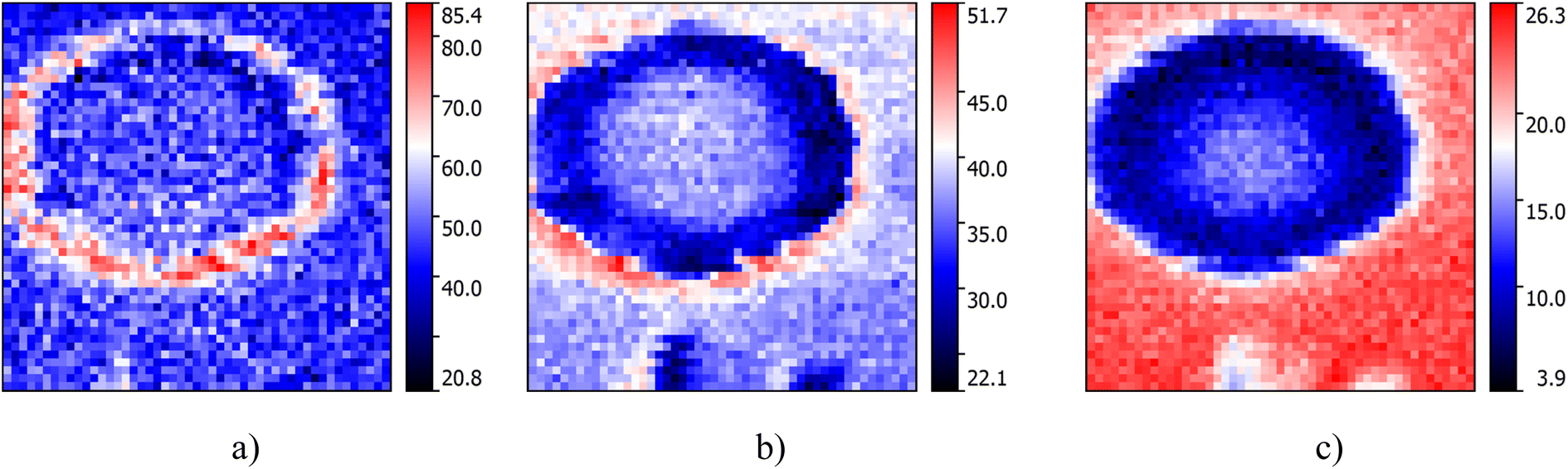 | ||
| Fig. 7 Amplitude nano-FTIR images for the phonon modes in the range of (a) 650–750 cm−1, (b) 750–800 cm−1, (c) 800–850 cm−1 with dimensions of 500 × 500 nm, 50 × 50 points recorded for the demodulation mode n = 2 with a mapping step of 10 nm. | ||
To explain the frequency shift of the phonon mode at the nanocrystal edge, we analytically calculated the surface optical modes in the nanocrystal, approximating it as an AlN cylinder, following the work of ref. 51, and the practical examples of this approach.20,54,55
According to ref. 51 and 54 the dispersion relation for SO modes ωSO(q), for which the cylinder length is not taken into account and q ≫ ω/c, can be determined from eqn (1):
 | (1) |
 | (2) |
Using eqn (1) and (2), the dispersion curves of SO modes of AlN nanocrystals in vacuum (εm = 1) were calculated and are shown in Fig. 8 along with the experimental TERS and nano-FTIR data. In the calculation, the diameter of the AlN nanocrystal was taken as 250 nm. This means that for TERS and nano-FTIR measurements, q·r is equal to 2.36 and 0.07 correspondingly due to significant differences in excitation wavelengths in Raman and IR experiments (638 and 12![[thin space (1/6-em)]](https://www.rsc.org/images/entities/char_2009.gif) 500 nm). The calculation results are presented in Fig. 8 by dashed lines. There are two important issues which need to be discussed. The first is the obvious disagreement between calculated and experimental SO phonon mode frequencies. The second is the regular downward shift of experimental SO mode frequencies derived from Raman data with respect to those obtained from IR measurements.
500 nm). The calculation results are presented in Fig. 8 by dashed lines. There are two important issues which need to be discussed. The first is the obvious disagreement between calculated and experimental SO phonon mode frequencies. The second is the regular downward shift of experimental SO mode frequencies derived from Raman data with respect to those obtained from IR measurements.
 | ||
| Fig. 8 (a) Theoretical frequency dependence of A1(SO) and E1(SO) modes on the wavevector multiplied by the radius. The calculated dispersion curves of SO modes of AlN nanocrystals placed in a vacuum (εm = 1) are shown by dashed lines. (b) The fragment of the dependence depicted in (a). Shadowed area indicates the frequency range (and the corresponding qr values), in which SO phonon modes are changed in IR measurements. | ||
The key parameters in the calculation are the dielectric functions of the nanocrystal and surrounding media. However, it is difficult to determine the dielectric constant of the medium around the sample. It depends on the excitation wavelength and measurements principles and is influenced by several factors:
• the values of the dielectric function of AlN for visible (638 nm) and IR regions (∼12500 nm) differ significantly;56,57
• for both TERS and nano-FTIR experiments, a tip made of a particular material (Ag and PtIr5, respectively) is placed in the vicinity of the AlN nanocrystal and changes the overall dielectric function;
• distances between the sample and the silver tip in TERS measurements in practical situation amount to about 1 nm,58 while nano-FTIR experiments are carried out in tapping mode with a sample-PtIr5 tip distance of usually more than 2 nm. Hence, the tip contributions to the dielectric function for TERS and nano-FTIR measurements are expected to be different;
• for nano-FTIR measurements, AlN reveals resonance absorption by optical phonons in the spectral range of the Reststrahlen band accompanied by a strong variation of its dielectric function.
Therefore, because of the uncertainties in the determination of the dielectric function surrounding the AlN nanocrystals we adjust the calculated dispersion curves to agree with the experimental SO phonon mode frequencies from both TERS and nano-FTIR data, thus varying the dielectric constant of the surrounding medium. The best agreement of calculated and experimental nano-FTIR and TERS results is presented in Fig. 8 by solid curves for the real part of dielectric constants of 0.017 ± 0.005 and 3.0 ± 0.2, respectively. A dielectric constant, which is close to zero for nano-FTIR measurements is not surprising and can be explained by the negative dielectric constant of the PtIr5 tip and the relative position of the tip and the sample during the nano-FTIR measurements, if effective medium approximation (EMA)47 is applicable, and the gap between the sample and tip considered to be filled with air εair ≈ 1. At the same time, similar arguments do not explain the effective dielectric constant of 3.0 for TERS experiments, as the dielectric constant exceeds the air value. One of the reasons for the large real dielectric constant can be a local surface plasmon resonance (LSPR) of the TERS tip. The energy of the LSPR is located in the red spectral region. However, the exact position of this resonance and therefore the value of the dielectric constant can not be exactly determined because the LSPR position depends on tip-sample distance.59 The other reason is that the EMA condition is not applicable in the case of our TERS measurements, and taking to account that the sample-tip gap in TERS measurement may be less than 1 nm, sophisticated analysis including quantum mechanics is required.59
During the nano-FTIR scanning across the AlN nanocrystal as shown in Fig. 6d, the tip moves along a flat surface producing SO mode of A1 symmetry at 768 cm−1 with qr = 0.07, crosses the inflection point, for which the SO mode at 725 cm−1 takes the minimum value with qr equal to 0.04, approaches the flat surface again on top of the nanocrystal, where SO mode frequency reaches the value of 768 cm−1 again as it can be seen from the evolution of nano-FTIR spectra (Fig. 6).
At the same time, the experimentally observed E1 mode at 830 cm−1 does not change position during the scanning of the sample, while our analytical model predicts the frequency shift in a similar manner as for A1 mode. This behavior can be associated with the dispersionless E1 mode with polarization along the Y axis (as shown in Fig. 6b). In this case, the change of wavevector in the ZX plane at the edge of the AlN nanocrystal does not influence the frequency of the E1 mode polarized along the Y direction.
4 Conclusions
We present a study of the phonon spectra of a single AlN nanocrystal with nanometer spatial resolution by two complementary optical methods, namely TERS and nano-FTIR spectroscopies. Both techniques demonstrate the ability to visualise a single AlN nanocrystal on the AlN surface based on a different optical response by SO modes from the AlN nanocrystal and the flat AlN surface activated in TERS and nano-FTIR measurements. TERS enhancement of SO modes in the nanocrystal originating from AlN optical phonons of A1 and E1 symmetries is demonstrated. Nano-FTIR spectra reveal a shift of the frequency position for the SO phonon mode of A1 symmetry when the nano-FTIR tip is approaching the nanocrystal edge. The frequency position of the SO mode depends on the curvature of the AlN nanocrystal that allows probing the angular dispersion of the phonons modes when the nano-IR tip moves across the AlN nanocrystal. Nano-FTIR imaging for different spectral regions enables establishing the spatial localisation of SO modes including the modes localized near the nanocrystal edges and the delocalised SO modes from the AlN layer. The results presented demonstrate the possibility of analysing nanoobjects by combining the advantages of non-destructive TERS and nano-FTIR spectroscopies with spatial resolution much below the diffraction limit, which is demanded for a wide variety of applications in electronics, chemistry, biology, and medicine.Conflicts of interest
There are no conflicts to declare.Acknowledgements
The authors gratefully acknowledge financial support from RFBR (Project No. 19-52-12041_NNIO_a) and the DFG grants ZA 146/43-1 and ZA 146/44-1. Experiments were carried out by using the equipment of the shared-user facility “Nanostructures” in the ISP Center. The studies were supported by the Ministry of Science and Higher Education of the Russian Federation, project #FSUS-2020-0029. The authors acknowledge core facilities “VTAN” (Novosibirsk State University) for the access to its experimental equipment.References
- G. Konstantatos and E. H. Sargent, Nat. Nanotechnol., 2010, 5, 391–400 CrossRef CAS PubMed.
- C. Tan, J. Chen, X. J. Wu and H. Zhang, Nat. Rev. Mater., 2018, 3, 1–13 CrossRef.
- J. Jeevanandam, A. Barhoum, Y. S. Chan, A. Dufresne and M. K. Danquah, Beilstein J. Nanotechnol., 2018, 9, 1050–1074 CrossRef CAS PubMed.
- C. Nan, W. Yue, L. Tao and X. Yang, Appl. Spectrosc. Rev., 2021, 56, 531–552 CrossRef CAS.
- P. Patoka, G. Ulrich, A. E. Nguyen, L. Bartels, P. A. Dowben, V. Turkowski, T. S. Rahman, P. Hermann, B. Kästner, A. Hoehl, G. Ulm and E. Rühl, Opt. Express, 2016, 24, 1154 CrossRef CAS PubMed.
- A. Blat, J. Dybas, M. Kaczmarska, K. Chrabaszcz, K. Bulat, R. B. Kostogrys, A. Cernescu, K. Malek and K. M. Marzec, Anal. Chem., 2019, 91, 9867–9874 CrossRef CAS PubMed.
- M. Yesiltas, T. D. Glotch and B. Sava, Sci. Rep., 2021, 11, 1–9 CrossRef PubMed.
- L. Mester, A. A. Govyadinov, S. Chen, M. Goikoetxea and R. Hillenbrand, Nat. Commun., 2020, 11, 3359 CrossRef CAS PubMed.
- M. Yesiltas, M. Kaya, T. D. Glotch, R. Brunetto, A. Maturilli, J. Helbert and M. E. Ozel, Meteorit. Planet. Sci., 2020, 55, 2404–2421 CrossRef CAS.
- P. Hermann, A. Hoehl, G. Ulrich, C. Fleischmann, A. Hermelink, B. Kästner, P. Patoka, A. Hornemann, B. Beckhoff, E. Rühl and G. Ulm, Opt. Express, 2014, 22, 17948 CrossRef PubMed.
- S. Amarie, P. Zaslansky, Y. Kajihara, E. Griesshaber, W. W. Schmahl and F. Keilmann, Beilstein J. Nanotechnol., 2012, 3, 312–323 CrossRef CAS PubMed.
- A. G. Milekhin, M. Rahaman, E. E. Rodyakina, A. V. Latyshev, V. M. Dzhagan and D. R. T. Zahn, Nanoscale, 2018, 10, 2755–2763 RSC.
- X. Wang, S. C. Huang, S. Hu, S. Yan and B. Ren, Nat. Rev. Phys., 2020, 2, 253–271 CrossRef.
- P. Verma, Chem. Rev., 2017, 117, 6447–6466 CrossRef CAS PubMed.
- R. A. Ferreyra, C. Zhu, A. Teke and H. Morkoç, in Group III Nitrides, Springer Handbooks, 2017, p. 1 Search PubMed.
- A. Rizzi, Appl. Surf. Sci., 2002, 190, 311–317 CrossRef CAS.
- M. S. Alias, M. Tangi, J. A. Holguin-Lerma, E. Stegenburgs, A. A. Alatawi, I. Ashry, R. C. Subedi, D. Priante, M. K. Shakfa, T. K. Ng and B. S. Ooi, J. Nanophotonics, 2018, 12, 1 Search PubMed.
- H. Harima, J. Phys.: Condens. Matter, J. Phys.: Condens. Matter, 2022, 14, R967–R993 CrossRef.
- V. Y. Davydov, Y. E. Kitaev, I. Goncharuk, A. Smirnov, J. Graul, O. Semchinova and D. Uffmann, Phys. Rev. B: Condens. Matter Mater. Phys., 1998, 58, 12899–12907 CrossRef CAS.
- S. Sahoo, S. Dhara, A. K. Arora, R. Krishnan, P. Chandramohan and M. P. Srinivasan, Appl. Phys. Lett., 2010, 96, 2010–2012 CrossRef.
- J. Frandon, J. Gleize, M. a Renucci and U. P. Sabatier, Encycl. Nanosci. Nanotechnol., 2004, 8, 513–526 CAS.
- E. O. Schäfer-Nolte, T. Stoica, T. Gotschke, F. A. Limbach, E. Sutter, P. Sutter, D. Grützmacher and R. Calarco, Nanotechnology, 2010, 21, 315702 CrossRef PubMed.
- R. Mata, A. Cros, K. Hestroffer and B. Daudin, Phys. Rev. B: Condens. Matter Mater. Phys., 2012, 85, 1–5 CrossRef.
- A. G. Milekhin, N. A. Yeryukov, L. L. Sveshnikova, T. A. Duda, E. I. Zenkevich, S. S. Kosolobov, A. V. Latyshev, C. Himcinski, N. V. Surovtsev, S. V. Adichtchev, Z. C. Feng, C. C. Wu, D. S. Wuu and D. R. T. Zahn, J. Exp. Theor. Phys., 2011, 113, 983–991 CrossRef CAS.
- R. Matsui, P. Verma, T. Ichimura, Y. Inouye and S. Kawata, Appl. Phys. Lett., 2007, 90, 88–91 CrossRef.
- N. Marquestaut, D. Talaga, L. Servant, P. Yang, P. Pauzauskie and F. Lagugné-Labarthet, J. Raman Spectrosc., 2009, 40, 1441–1445 CrossRef CAS.
- H. Siegle, L. Eckey, A. Hoffmann, C. Thomsen, B. K. Meyer, D. Schikora, M. Hankeln and K. Lischka, Solid State Commun., 1995, 96, 943–949 CrossRef CAS.
- S. Berweger and M. B. Raschke, J. Raman Spectrosc., 2009, 40, 1413–1419 CrossRef CAS.
- E. Poliani, M. R. Wagner, A. Vierck, F. Herziger, C. Nenstiel, F. Gannott, M. Schweiger, S. Fritze, A. Dadgar, J. Zaumseil, A. Krost, A. Hoffmann and J. Maultzsch, J. Phys. Chem. Lett., 2017, 8, 5462–5471 CrossRef CAS PubMed.
- A. Patsha, S. Dhara and A. K. Tyagi, Appl. Phys. Lett., Appl. Phys. Lett., 2015, 107, 123108 CrossRef.
- S. Parida, A. Patsha, K. K. Madapu and S. Dhara, J. Appl. Phys., 2020, 127, 173103 CrossRef CAS.
- E. Poliani, D. Seidlitz, M. Ries, S. J. Choi, J. S. Speck, A. Hoffmann and M. R. Wagner, J. Phys. Chem. C, 2020, 124, 28178–28185 CrossRef CAS.
- A. K. Sivadasan, A. Patsha, A. Maity, T. K. Chini and S. Dhara, J. Phys. Chem. C, 2017, 121, 26967–26975 CrossRef CAS.
- A. G. Milekhin, L. L. Sveshnikova, T. A. Duda, N. A. Yeryukov, E. E. Rodyakina, A. K. Gutakovskii, S. A. Batsanov, A. V. Latyshev and D. R. T. Zahn, Phys. E, 2016, 75, 210–222 CrossRef CAS.
- E. Poliani, M. R. Wagner, J. S. Reparaz, M. Mandl, M. Strassburg, X. Kong, A. Trampert, C. M. Sotomayor Torres, A. Hoffmann and J. Maultzsch, Nano Lett., 2013, 13, 3205–3212 CrossRef CAS PubMed.
- R. Hillenbrand, T. Taubner and F. Keilmann, Nature, 2002, 418, 159–162 CrossRef CAS PubMed.
- A. M. Gigler, A. J. Huber, M. Bauer, A. Ziegler, R. Hillenbrand and R. W. Stark, Opt. Express, 2009, 17, 22351 CrossRef CAS PubMed.
- S. Bensmann, F. Gaußmann, M. Lewin, J. Wüppen, S. Nyga, C. Janzen, B. Jungbluth and T. Taubner, Opt. Express, 2014, 22, 22369 CrossRef PubMed.
- A. Huber, N. Ocelic, T. Taubner and R. Hillenbrand, Nano Lett., 2006, 6, 774–778 CrossRef CAS PubMed.
- I. A. Milekhin, A. S. Kozhukhov, D. V. Sheglov, L. I. Fedina, A. G. Milekhin, A. V. Latyshev and D. R. T. Zahn, Appl. Surf. Sci., 2022, 584, 152583 CrossRef CAS.
- T. Livneh, J. Zhang, G. Cheng and M. Moskovits, Phys. Rev. B: Condens. Matter Mater. Phys., 2006, 74, 1–10 CrossRef.
- A. Ishizaka and Y. Shiraki, J. Electrochem. Soc., 1986, 133, 666–671 CrossRef CAS.
- V. G. Mansurov, T. V. Malin, Y. G. Galitsyn, A. A. Shklyaev and K. S. Zhuravlev, J. Cryst. Growth, 2016, 441, 12–17 CrossRef CAS.
- V. G. Mansurov, Y. G. Galitsyn, T. V. Malin, S. A. Teys, K. S. Zhuravlev, I. Cora and B. Pecz, in 2D Materials, IntechOpen, 2019, pp. 1–19 Search PubMed.
- L. S. Basalaeva, N. N. Kurus, E. E. Rodyakina, K. V Anikin and A. G. Milekhin, J. Phys.: Conf. Ser., 2021, 2015, 012013 CrossRef CAS.
- N. Ocelic, A. Huber and R. Hillenbrand, Appl. Phys. Lett., 2006, 89, 101124 CrossRef.
- A. A. Govyadinov, I. Amenabar, F. Huth, P. Scott Carney and R. Hillenbrand, J. Phys. Chem. Lett., 2013, 4, 1526–1531 CrossRef CAS PubMed.
- P. A. Temple and C. E. Hathaway, Phys. Rev. B: Solid State, 1973, 7, 3685–3697 CrossRef CAS.
- W. Zheng, R. Zheng, F. Huang, H. Wu and F. Li, Photonics Res., 2015, 3, 38 CrossRef CAS.
- A. Zwick and R. Carles, Phys. Rev. B: Condens. Matter Mater. Phys., 1993, 48, 6024–6032 CrossRef CAS PubMed.
- B. E. Sernelius, Surface Modes in Physics, Wiley, New York, 2001 Search PubMed.
- J. Shao and W. Su, Nanoscale, 2022, 14, 17119–17133 RSC.
- K. F. Domke and B. Pettinger, ChemPhysChem, 2010, 11, 1365–1373 CrossRef CAS PubMed.
- R. Gupta, Q. Xiong, G. D. Mahan and P. C. Eklund, Nano Lett., 2003, 3, 1745–1750 CrossRef CAS.
- A. K. Sivadasan, C. Singha, K. G. Raghavendra, S. Amirthapandian, A. Bhattacharyya, A. Dasgupta and S. Dhara, Appl. Phys. A: Mater. Sci. Process., 2017, 123, 1–8 CrossRef CAS.
- P. B. Johnson and R. W. Christy, Phys. Rev. B: Solid State, 1972, 6, 4370–4379 CrossRef CAS.
- A. D. Rakić, A. B. Djurišić, J. M. Elazar and M. L. Majewski, Appl. Opt., 1998, 37, 5271 CrossRef PubMed.
- M. Rahaman, A. G. Milekhin, V. Dzhagan, D. R. Zahn, A. Mukherjee, E. E. Rodyakina and A. Latyshev, Faraday Discuss., 2019, 214, 309–323 RSC.
- B. Pettinger, K. F. Domke, D. Zhang, G. Picardi and R. Schuster, Surf. Sci., 2009, 603, 1335–1341 CrossRef CAS.
| This journal is © The Royal Society of Chemistry 2023 |