
 Open Access Article
 This Open Access Article is licensed under a
 Creative Commons Attribution 3.0 Unported Licence
Revealing the electronic, optical and photocatalytic properties of PN-M2CO2 (P = Al, Ga; M = Ti, Zr, Hf) heterostructures
M.
Munawar
 a,
M.
Idrees
a,
Tahani A.
Alrebdi
*b and
B.
Amin
*a
a,
M.
Idrees
a,
Tahani A.
Alrebdi
*b and
B.
Amin
*a
aDepartment of Physics, Abbottabad University of Science & Technology, Abbottabad 22010, Pakistan. E-mail: binukhn@gmail.com
bDepartment of Physics, College of Science, Princess Nourah Bint Abdulrahman University, P.O. Box 84428, Riyadh 11671, Saudi Arabia. E-mail: taalrebdi@pnu.edu.pk
First published on 2nd February 2023
Abstract
Using DFT, the electronic structure, optical, and photocatalytic properties of PN (P = Ga, Al) and M2CO2 (M = Ti, Zr, Hf) monolayers and their PN-M2CO2 van der Waals heterostructures (vdWHs) are investigated. Optimized lattice parameters, bond length, bandgap, conduction and valence band edges show the potential of PN (P = Ga, Al) and M2CO2 (M = Ti, Zr, Hf) monolayers in photocatalytic applications, and the application of the present approach to combine these monolayers and form vdWHs for efficient electronic, optoelectronic and photocatalytic applications is shown. Based on the same hexagonal symmetry and experimentally achievable lattice mismatch of PN (P = Ga, Al) with M2CO2 (M = Ti, Zr, Hf) monolayers, we have fabricated PN-M2CO2 vdWHs. Binding energies, interlayer distance and AIMD calculations show the stability of PN-M2CO2 vdWHs and demonstrate that these materials can be easily fabricated experimentally. The calculated electronic band structures show that all the PN-M2CO2 vdWHs are indirect bandgap semiconductors. Type-II[-I] band alignment is obtained for GaN(AlN)-Ti2CO2[GaN(AlN)-Zr2CO2 and GaN(AlN)-Hf2CO2] vdWHs. PN-Ti2CO2 (PN-Zr2CO2) vdWHs with a PN(Zr2CO2) monolayer have greater potential than a Ti2CO2(PN) monolayer, indicating that charge is transfer from the Ti2CO2(PN) to PN(Zr2CO2) monolayer, while the potential drop separates charge carriers (electron and holes) at the interface. The work function and effective mass of the carriers of PN-M2CO2 vdWHs are also calculated and presented. A red (blue) shift is observed in the position of excitonic peaks from AlN to GaN in PN-Ti2CO2 and PN-Hf2CO2 (PN-Zr2CO2) vdWHs, while significant absorption for photon energies above 2 eV for AlN-Zr2CO2, GaN-Ti2CO2 and PN-Hf2CO2, give them good optical profiles. The calculated photocatalytic properties demonstrate that PN-M2CO2 (P = Al, Ga; M = Ti, Zr, Hf) vdWHs are the best candidates for photocatalytic water splitting.
I. Introduction
Photocatalytic water splitting is considered as the most suitable way to convert sunlight into chemical energy in the form of hydrogen.1 Therefore, understanding the mechanism of photocatalytic water splitting and exploring new photocatalysts are of interest for both fundamental research and industrial applications.2 Light harvesting, separation, and diffusion of photogenerated carriers (electrons and holes) to the surface, and hydrogen and oxygen evaluation reactions are the major steps in photocatalysis. A suitable bandgap3 to strengthen (weaken) electron–hole separation (recombination) time,4 and band edge positions (straddling the redox potential of water) of a potential semiconductor photocatalyst, are key in order to achieve the overall water splitting process.5In the case of two-dimensional (2D) materials, a large surface area provides a shorter route for photogenerated electron–hole pairs to flow to the surface and facilitate a redox reaction, hence increasing the lifetime of carriers. Therefore, 2D materials are considered as pioneer candidates for photocatalytic water splitting as compared to their bulk counterparts.6 Performance of 2D materials is not limited to photocatalytic water splitting, and is also gaining much attention in both optoelectronics and thermoelectric device applications.7,8 In the family of 2D materials, MXenes produced by etching the A layer from the MAX phase,9 have a rich surface with functional groups (O, OH, F), responsible for excellent electronic,10 optical,11 electrochemical,12 and mechanical properties13,14 in catalysis,15 energy storage,16 batteries,17 photocatalytic water splitting18 and other related fields.19 Another group of the 2D family, PN (P = Al, Ga) monolayers, are excellent candidates as compared to their bulk counterparts, due to their thin structure, high active surface, high stability, large energy bandgap, blue-shifted photoluminescence peaks, high internal quantum efficiency and transfer of charge from Al/Ga to N.20–23 Experimentally, AlN is prepared by CVD, MBE and PVT techniques,24 while GaN is prepared by a migration enhanced encapsulated growth technique.25 Structural stability of the PN (P = Al, Ga) monolayer are further confirmed by phonon spectrum calculations.26,27 Strain engineering can also be performed to tune the bandgap of PN monolayers without structure distortion.28,29 PN (P = Al, Ga) nanowire,30,31 nanosheets32,33 and nanoribbons,34,35 have also been reported with fascinating properties.
The emergence of vdWHs in the 2D field offers a new way to combine different monolayers for novel electronic, optoelectronic, and photocatalytic applications.36,37 Some vdWHs based on MXene, AlN, and GaN like MoS2/MXene,38 TiO2/Mxenes,39 MXene/graphene,40 TMDCs/MXenes,41 SiS/MXenes,42 BSe/MXenes,43 AlGaN/GaN,44 MoSe2/GaN,45 AlN/GaN,46 WS2/GaN,47 ZnO/GaN,48 graphene/AlN,49 BP/AlN,50 and AlN/InSe,51 have already been fabricated for practical device applications. Electronic structure, optical properties and overall water splitting performance of GaN/Hf2CO2 and AlN/Hf2CO2 vdWHs have been investigated in ref. 52 and 53. A type-II band alignment for full water splitting is also observed in boron phosphide-blue phosphorene,54 C2N-based type-II heterojunctions55 and other 2D materials.56
From this aspect, surprisingly no investigation has addressed PN-M2CO2 (P = Al, Ga; M = Ti, Zr) vdWHs. Therefore, based on the same hexagonal symmetry, small lattice mismatch and unique performance of all MXenes of group M2CO2 (M = Ti, Zr, Hf) and PN (P = Al, Ga) monolayers, we combine these monolayers, in the form PN-M2CO2 (P = Al, Ga; M = Ti, Zr, Hf) vdWHs. A detailed study is gained to explore the electronic structure, optical and photocatalytic properties of PN-M2CO2 (P = Al, Ga; M = Ti, Zr, Hf) vdWHs. Our investigation revealed that all these six heterostructures are promising candidates for photocatalytic and optoelectronic devices.
II. Computational details
We employ DFT![[thin space (1/6-em)]](https://www.rsc.org/images/entities/char_2009.gif) 57 in VASP,58 with PBE59 and HSE0660 functionals for both atomic relaxation and electronic bandstructure calculations. These calculations are performed with a conjugate gradient algorithm to minimize the atomic forces (energy) with a tolerance of 0.01 eV Å−1 (10−4 eV). A cut-off energy of 500 eV, Γ-centered k-point mesh of 8 × 8 × 1, and a vacuum of 25 Å along the z-direction were used to ensure a negligible interaction between adjacent layers.
57 in VASP,58 with PBE59 and HSE0660 functionals for both atomic relaxation and electronic bandstructure calculations. These calculations are performed with a conjugate gradient algorithm to minimize the atomic forces (energy) with a tolerance of 0.01 eV Å−1 (10−4 eV). A cut-off energy of 500 eV, Γ-centered k-point mesh of 8 × 8 × 1, and a vacuum of 25 Å along the z-direction were used to ensure a negligible interaction between adjacent layers.
AIMD61 simulations were used to investigate the thermal stabilities of PN-M2CO2 (P = Al, Ga; M = Ti, Zr, Hf) vdWHs through the nose thermostat algorithm at 300 K. The system was allowed to relax for 12 picoseconds with a time step of 3 femtoseconds.62,63
The Bethe–Salpeter equation (BSE) is also solved in the GW0 calculation64 using the epsilon package65 in Quantum Espresso66 to obtain ε2(ω). Furthermore, using the turbo Lanczos algorithm,67 we investigated the absorption coefficient (α) to understand the optical behaviour of these systems in detail.68
III. Results and discussion
Optimized geometry (top and side view) and electronic bandstructure in Fig. 1, show that PN (P = Al, N) and M2CO2 (M = Ti, Zr, Hf) monolayers are indirect bandgap semiconductors. In the case of the PN (P = Ga, Al) monolayer, the CBM (VBM) lies at the Γ(K)-point, while for M2CO2 the VBM lies at the Γ-point and the CBM is between the K and M point of the first BZ, consistent with ref. 43 and 69. The photocatalytic response in Fig. 2, shows that Ti2CO2 and Zr2CO2 cross (fail to cross) the valence (conduction) band edge, while both the PN and Hf2CO2 monolayers cross both the conduction and valence band edges (see also Table 1), in agreement with ref. 43. These results show the potential of PN (M = Ga, Al) and M2CO2 (M = Ti, Zr, Hf) monolayers in photocatalytic applications and the authenticity of the present approach to combine these monolayers to form vdWHs for efficient electronic, optoelectronic and photocatalytic applications.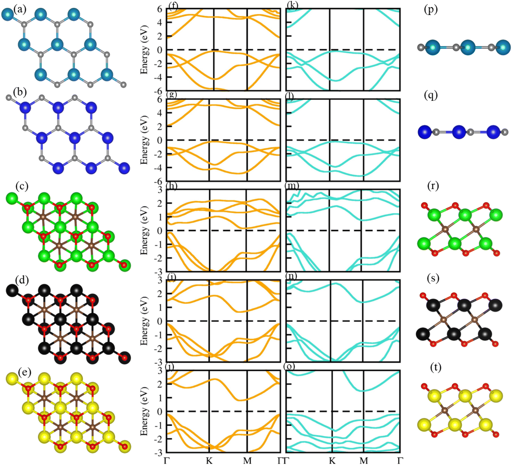 | ||
| Fig. 1 Geometrical structure (top view in first column), electronic bandstructure (PBE in second column; HSE06 in third column) and side view (fourth column) of GaN ((a), (f), (k), (p)), AlN ((b), (g), (i), (q)), Ti2CO2 ((c), (h), (m), (r)), Zr2CO2 ((d), (j), (n), (s)) and Hf2CO2 ((e), (j), (o), (t)). | ||
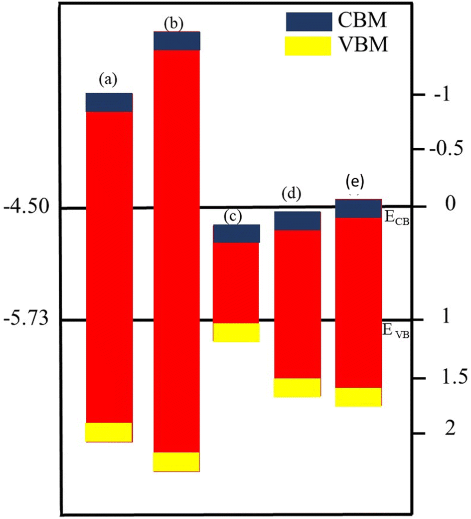 | ||
| Fig. 2 Band alignment for the valence band (VB) and conduction band (CB) edge of (a) GaN, (b) AlN, (c) Ti2CO2, (d) Zr2CO2 and (e) Hf2CO2 monolayers. | ||
| Monolayers | GaN | AlN | Ti2CO2 | Zr2CO2 | Hf2CO2 |
|---|---|---|---|---|---|
| a | 3.255 | 3.288 | 3.01 | 3.31 | 3.27 |
| Ga–N | 1.894 | — | — | — | — |
| Al–N | — | 1.807 | — | — | — |
| M–O | — | — | 1.97 | 2.119 | 2.091 |
| M–C | — | — | 2.21 | 2.359 | 2.332 |
| E g (PBE) | 1.98 | 2.35 | 0.3 | 0.865 | 0.99 |
| E g (HSE06) | 3.23 | 3.98 | 0.95 | 1.57 | 1.69 |
| E CB | −1.0022 | −1.6823 | 0.3398 | 0.0798 | −0.002 |
| E VB | 2.1977 | 2.3176 | 1.2898 | 1.6498 | 1.6923 |
Although the lattice mismatch of GaN(AlN) with Ti2CO2 is 7.52 (8.45)%, with Zr2CO2 is 1.66 (0.90)% and with Hf2CO2 is 0.45 (0.30)%, these are experimentally achievable70 in the fabrication of PN-M2CO2 vdWHs. But controlling the orientation of layers while fabricating vdWHs using mechanical exfoliation is quite difficult. Moreover, the electronic bandstructure is very sensitive to the stacking of layers. Therefore, we fabricated four different stacking patterns of PN-M2CO2 (P = Ga, Al; M = Ti, Zr, Hf) vdWHs, as presented in Fig. 3. In stacking (a), the M(O) atom of the M2CO2 layer is placed on the top of Ga/Al(N) atom of the PN layer; in stacking (b), the M(O) atom of the M2CO2 layer is placed on top of the N(Ga/Al) atom of the PN layer; in stacking (c), the M(C) atom of the M2CO2 layer is placed on top of the N(Ga/Al) of the PN layer; and stacking (d) is the reciprocal of stacking (c). The magnitude of the binding energy (Eb = EPN-M2CO2 − EM2CO2 − EPN, where EPN-M2CO2 is the total energy of the vdWHs, EM2CO2 is the total energy of the isolated M2CO2 monolayer, and EPN is the total energy of the isolated PN monolayer) and the interlayer distance, show the disparity between different stacking patterns. The shorter the interlayer distance and the smaller the binding energy, corresponds to a more stable configuration, see Table 2. Therefore, stacking (d) of PN-M2CO2 vdWHs is the most favorable stacking configuration. Negative binding energy confirms that formation of PN-M2CO2 vdWHs are exothermic.71–73 The optimized lattice constants and bond lengths for the most stable stacking configuration are given in Table 3.
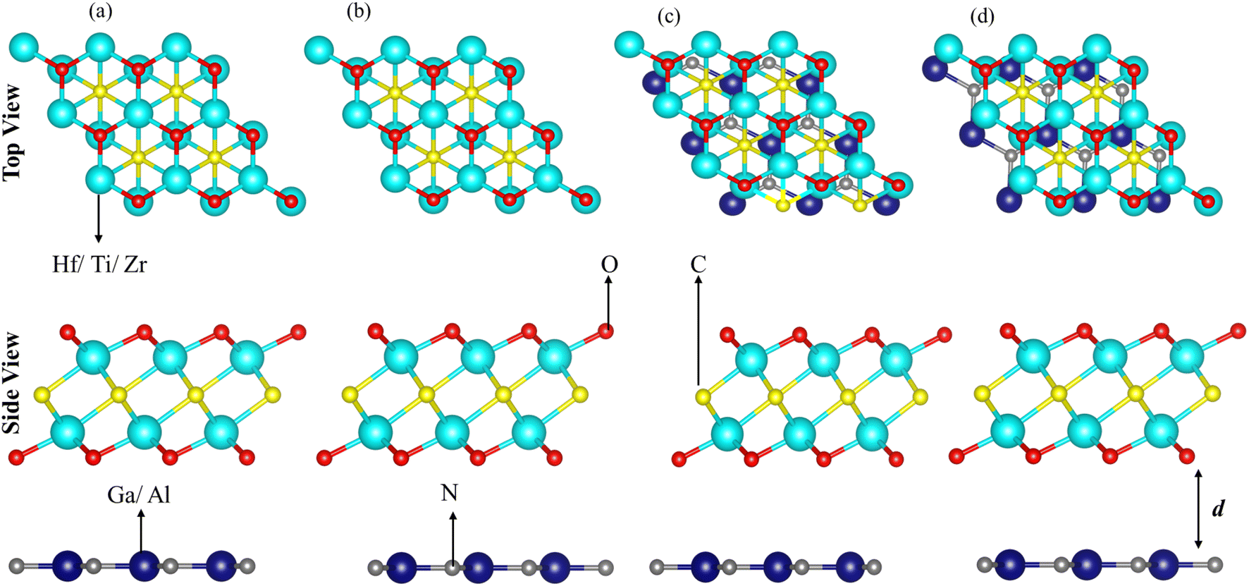 | ||
| Fig. 3 Possible stacking configurations of PN (P = Ga, Al) and M2CO2 (M = Ti, Zr, Hf) vdWHs. | ||
| Stacking | GaN-Ti2CO2 | GaN-Zr2CO2 | GaN-H2CO2 | AlN-Ti2CO2 | AlN-Zr2CO2 | AlN-Hf2CO2 |
|---|---|---|---|---|---|---|
| E b(a) | −0.808 | −0.116 | −0.141 | −0.739 | −0.962 | −0.064 |
| d | 3.26 | 3.33 | 3.37 | 4.305 | 3.28 | 3.289 |
| E b(b) | −0.818 | −0.157 | −0.182 | −0.324 | −0.359 | −0.064 |
| d | 3.24 | 3.246 | 3.24 | 3.31 | 3.3 | 3.39 |
| E b(c) | −0.813 | −0.117 | −0.003 | −0.055 | −0.939 | −0.064 |
| d | 3.27 | 3.28 | 3.29 | 3.28 | 3.25 | 3.29 |
| E b(d) | −0.833 | −0.217 | −0.382 | −0.884 | −1.062 | −0.104 |
| d | 3.05 | 3.21 | 3.19 | 3.24 | 3.22 | 3.23 |
 and
and  ), conduction and valence band edges (ECB and EVB in eV) of PN-M2CO2 (P = Ga, Al; M = Ti, Zr, Hf) vdWHs
| Heterostructure | a | E g-PBE | E g-HSE | ΔV | ϕ |
|
|
E CB | E VB |
|---|---|---|---|---|---|---|---|---|---|
| GaN-Ti2CO2 | 3.31 | 0.14 | 0.65 | 0.71 | 6.46 | 1.07 | 2.59 | 0.35 | 1.0 |
| GaN-Zr2CO2 | 3.28 | 0.81 | 1.62 | 10.44 | 7.60 | 1.30 | 2.43 | −0.11 | 1.51 |
| GaN-Hf2CO2 | 3.26 | 0.91 | 1.69 | 2.44 | 5.67 | 1.20 | 1.40 | −0.15 | 1.53 |
| AlN-Ti2CO2 | 3.15 | 0.60 | 1.15 | 11.01 | 6.17 | 3.44 | 3.01 | 0.12 | 1.27 |
| AlN-Zr2CO2 | 3.30 | 0.84 | 1.85 | 0.41 | 7.31 | 1.47 | 2.31 | −0.03 | 1.46 |
| AlN-Hf2CO2 | 3.28 | 0.88 | 1.79 | 8.02 | 5.50 | 1.24 | 1.54 | −0.183 | 1.60 |


Further, the thermal stability of stacking (d) of PN-M2CO2 vdWHs, is verified using AMID simulation with 3 × 3 × 1 supercell, (see top view of the structures, before and after heating in Fig. 4). It is clear that after heating for 5 ps at 1 fs time stops at 300 K, all six of the most stable configuration patterns of PN-M2CO2 vdWHs show no broken bonds (Fig. 4, column 3), while free energy oscillates slightly (Fig. 4, column 2), and hence confirms the thermal stability of understudy vdWHs. Therefore, stacking (d) is the most stable stacking configuration and is further investigated in detail.
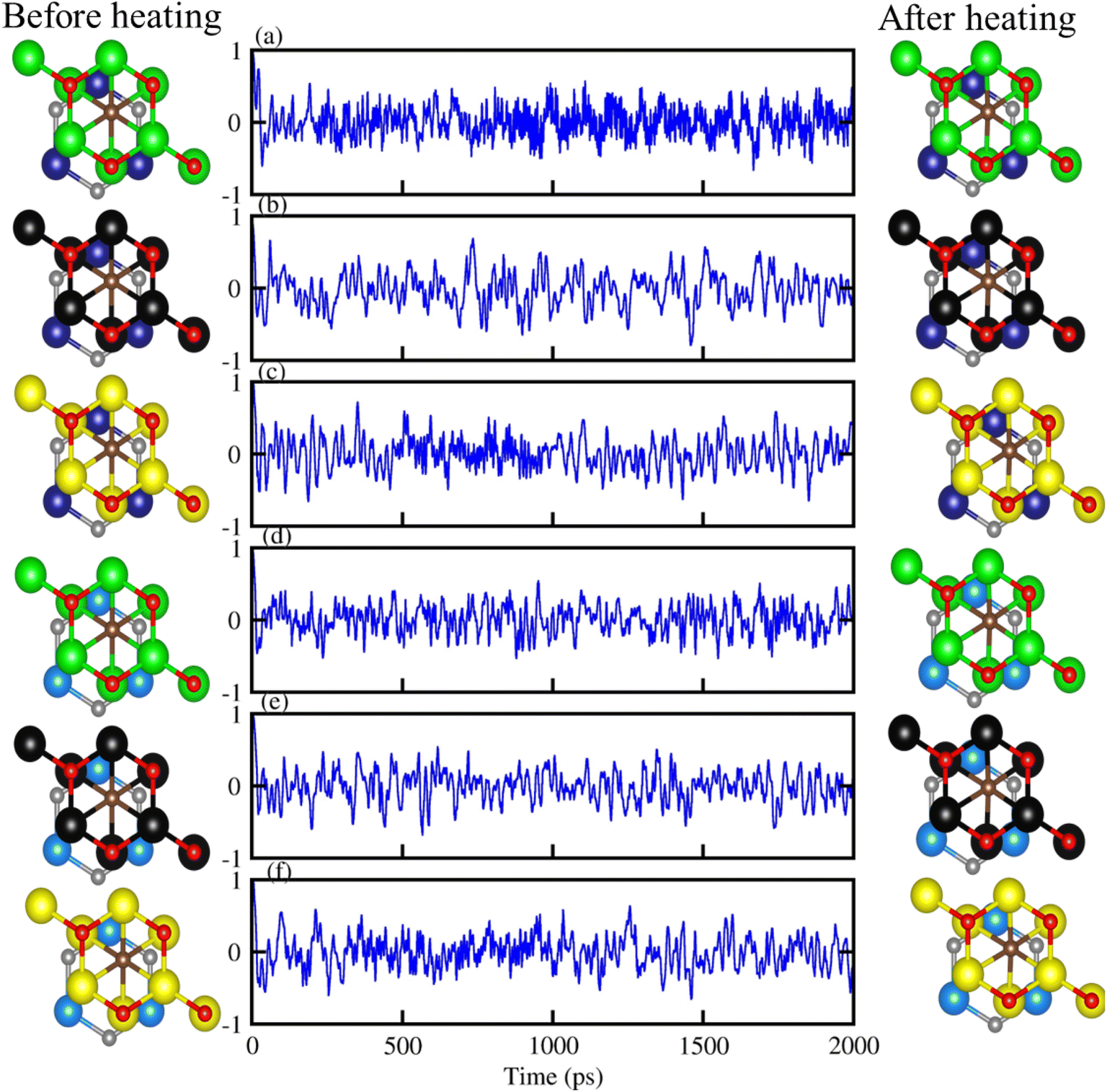 | ||
| Fig. 4 Geometrical structure before heating (first column), with fluctuating energy (second column) and after heating (third column) of: (a) GaN-Ti2CO2, (b) GaN-Zr2CO2, (c) GaN-Hf2CO2, (d) AlN-Ti2CO2, (e) AlN-Zr2CO2 and (f) AlN-Hf2CO2 vdWHs using AIMD simulation. | ||
The behavior of the bandstructure and bandgap values are dependent on exchange correlation functionals.74 Therefore, we have calculated the bandstructure of PN-M2CO2 vdWHs using both PBE and HSE06 functionals, see Fig. 5, with the bandgap values listed in Table 3. One can see that HSE06 band gap values are larger than those of the PBE method, as the PBE approach underestimates the band gap values of semiconductors. For PN-Ti2CO2(GaN-Zr2CO2 and PN-Hf2CO2) vdWHs, the VBM lies at the K–M(Γ)-point and the CBM at the Γ(K–M)-point of the first BZ. For AlN-Zr2CO2, both the VBM and CBM lie at the K–M point of the first BZ. These results show that all the vdWHs are indirect bandgap semiconductors, where electrons must undergo a significant change in momentum for a photon of energy (Eg) to create an electron–hole pair.75 In the case of indirect bandgap semiconductors, the electron interacts with the photon (phonon) to gain (gain or lose) energy (momentum). Hence, the position of the CBM and VBM can be aligned using suitable light according to the bandgap, and a transition is possible at lower energy using phonons, making them useful for laser applications.76–78
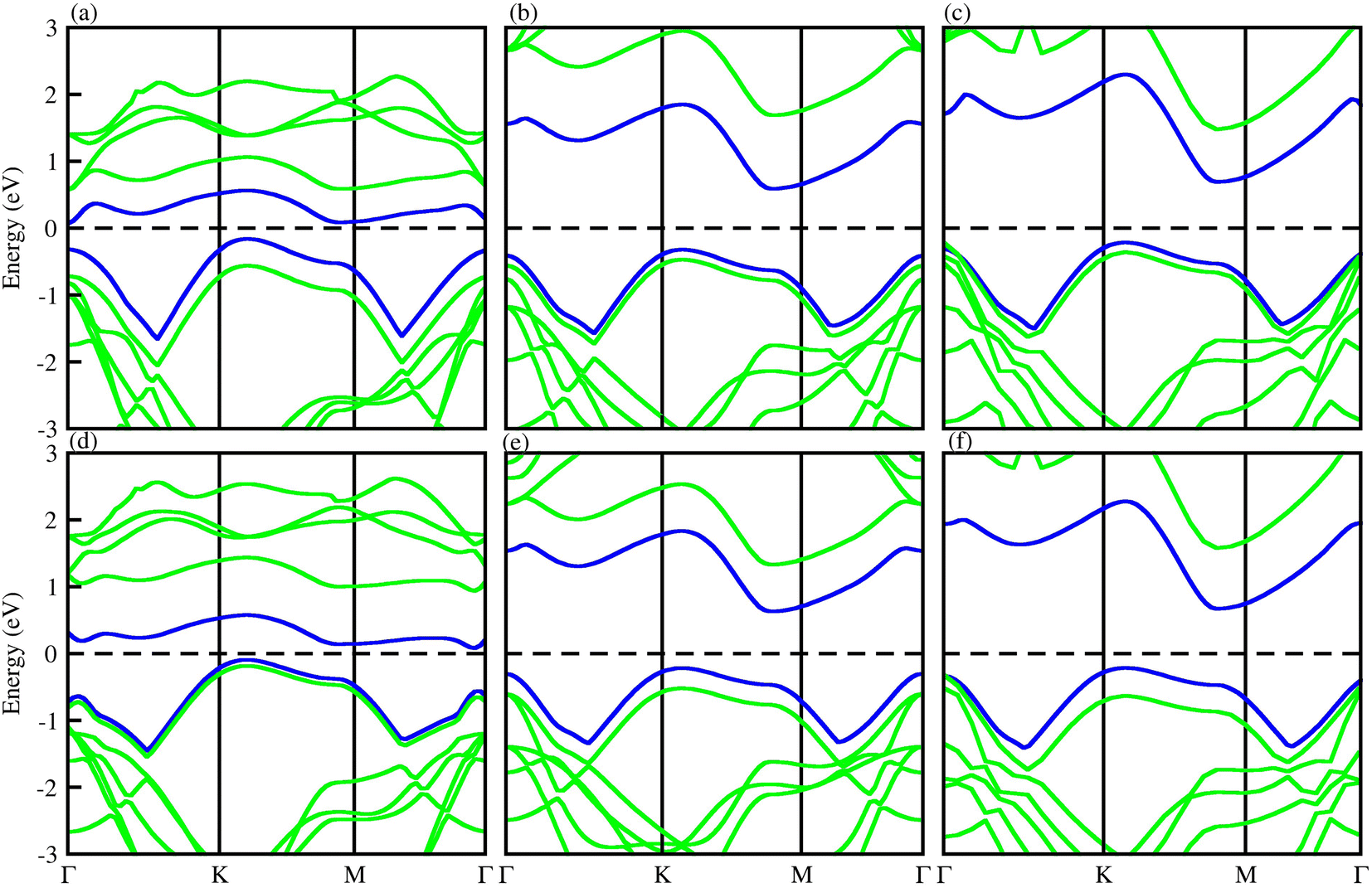 | ||
| Fig. 5 PBE (blue) and HSE06 (green) band structures of (a) GaN-Ti2CO2, (b) GaN-Zr2CO2, (c) GaN-Hf2CO2, (d) AlN-Ti2CO2, (e) AlN-Zr2CO2 and (f) AlN-Hf2CO2 vdWHs. | ||
To check the atomic states in the CBM/VBM at the Fermi level and band alignment, we plotted the partial density of states (PDOS) for PN-M2CO2 (P = Ga, Al; M = Hf, Ti and Zr) vdWHs, see Fig. 6. In the case of PN-Ti2CO2, the VBM (CBM) is from the NP (Tid) state of the PN(Ti2CO2) monolayer confirming type-II band alignment. The relative band position allows the mobility of electron (holes) from the conduction (valence) band of Ti2CO2(PN) to the conduction (valence) band of the PN(Ti2CO2) monolayer, offering a potential technique for charge separation. Hence, PN-Ti2CO2 vdWHs are promising candidates for solar energy conversion.79 In the case of PN-Zr2CO2(Hf2CO2), the VBM and CBM is due to the Cp state and the Zr/Hfd state, indicating type-I band alignment, as the CBM and VBM is from the same monolayer. Both the electron and hole from the PN is transported to Zr2CO2(Hf2CO2), so would not provide good charge separation. However, since the Fermi level of semiconductors tune the band alignment (for non-intrinsic semiconductors), the carrier (electrons and holes) movement can be hindered in a certain direction (depending on the internal electric field direction); that is, electrons may be transported to Zr2CO2(Hf2CO2), but hole movement to Zr2CO2(Hf2CO2) is hindered. Hence, the resulting charge separation makes the materials the best candidates for light emission applications.80
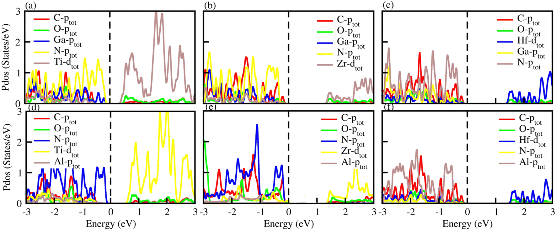 | ||
| Fig. 6 PDOS of (a) GaN-Ti2CO2, (b) GaN-Zr2CO2, (c) GaN-Hf2CO2, (d) AlN-Ti2CO2, (e) AlN-Zr2CO2 and (f) AlN-Hf2CO2 vdWHs. | ||
The average electrostatic potential shown in Fig. 7 shows that in the case of the PN-Ti2CO2 (PN-Zr2CO2) vdWH, the PN(Zr2CO2) monolayer has deeper potential than the Ti2CO2(PN) monolayer, indicating that charge is transferred from the Ti2CO2(PN) monolayer to the PN(Zr2CO2) monolayer. Meanwhile, in the case of GaN-Hf2CO2 (AlN-Hf2CO2), the Hf2CO2(AlN) monolayer has deeper potential than GaN(Hf2CO2), showing that charge is transferred from GaN(Hf2CO2) to Hf2CO2(AlN). The potential drop across the vdWHs (see Table 3) separates charge carriers (electron and holes) at the interface.81,82 Fabrication of the vdWHs enhances the electronic properties of the corresponding monolayers, hence effectively modulating the work function (ϕ). It also changes with strain and electric field engineering and doping.83 So, we have calculated the work function (ϕ = Evec − EF, where Evec (EF) represent the vacuum potential which is derived from the electrostatic potential (Fermi energy)) for all PN-M2CO2 (P = Ga, Al; M = Ti, Zr, Hf) vdWHs, see Fig. 7 and Table 3. The calculated work function of PN-M2CO2 vdWHs is almost the average of the corresponding monolayers (PN (P = Ga, Al) and M2CO2 (M = Ti, Zr, Hf)), which is efficient for the transfer of charge. The effective mass of the electron and holes for PN-M2CO2(P = Ga, Al; M = Ti, Zr, Hf) vdWHs are also calculated and are presented in Table 3. Materials with lower effective mass and high carrier mobility, are strongly preferred for high performance electronic devices,84 while a large effective mass greatly suppresses the quantum tunnelling, hence these materials are more appealing for logic devices.85 For AlN-Ti2CO2 the effective mass of electrons and holes is greater and is suggested for logic devices, while for the rest of the vdWHs the effective mass of electrons and holes is less than AlN-Ti2CO2, and is considered to be the best for high performance electronic devices.
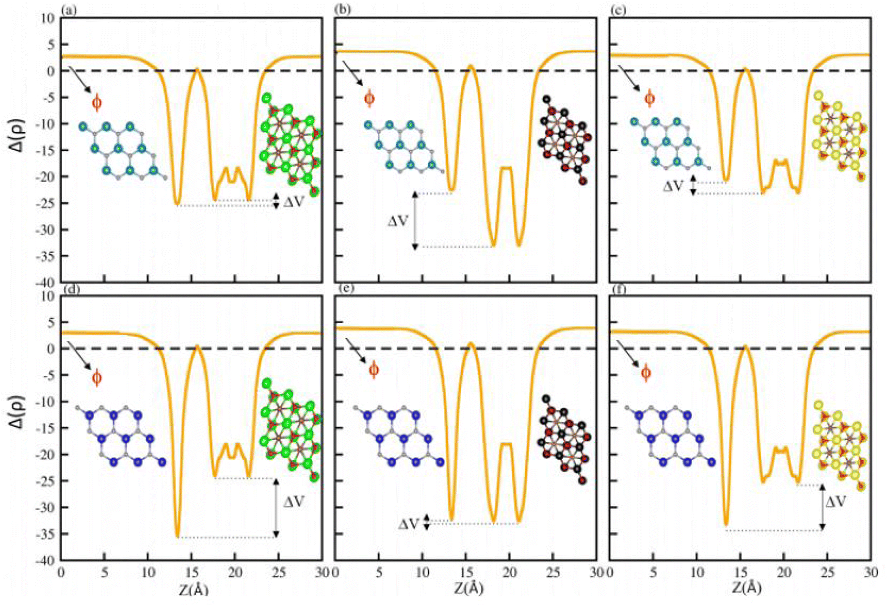 | ||
| Fig. 7 Average electrostatic potential of (a) GaN-Ti2CO2, (b) GaN-Zr2CO2, (c) GaN-Hf2CO2, (d) AlN-Ti2CO2, (e) AlN-Zr2CO2 and (f) AlN-Hf2CO2 vdWHs. The work function (ϕ) and potential drop (ΔV) are highlighted. | ||
The optical properties of materials define how materials react to incident electromagnetic radiation. We used DFT-PBE simulations to calculate optical features of PN-M2CO2 (P = Al, Ga; M = Ti, Zr, Hf) vdWHs such as the imaginary part of the dielectric function (ε2(ω) in Fig. 8) and absorption coefficients (α(ω) in Fig. 9). The observed excitonic peaks appear at 2.0 (1.9) eV and 2.8 (2.2) eV for AlN-Ti2CO2 (GaN-Ti2CO2) vdWHs; at 2.2 (2.2) eV and 3.7 (3.8) eV for AlN-Zr2CO2 (GaN-Zr2CO2) vdWHs; at 2.7 (2.2) eV and 3.7 (2.3) eV for AlN-Hf2CO2 (GaN-Hf2CO2) vdWHs. A red (blue) shift is observed in the position of excitonic peaks from AlN to GaN in PN-Ti2CO2 and PN-Hf2CO2 (PN-Zr2CO2) vdWHs. Furthermore, absorption coefficient α (μm−1) provides the photon power attenuation when it passes through the material. It also tells us how far light of specific energy and wavelength can spike the surface of the material before being absorbed.86,87 Although absorption is mainly determined by ε2(ω), this generalization is obviously not valid if the medium has very large α(ω).88 Therefore, we have further calculated the α(ω) of PN-M2CO2 (P = Ga, Al; M = Ti, Zr, Hf) vdWHs, as presented in Fig. 9, using the Lanczos program to solve the recursively quantum Liouville equation in the standard batch representation, which allows us to avoid interactions and multiplications of large matrices.89 The obtained values for α(ω) show that there is significant absorption for photon energies above 2 eV for AlN-Zr2CO2, GaN-Ti2CO2 and PN-Hf2CO2, making them candidates with a good optical profile. While in the case of AlN-Ti2CO2 and GaN-Zr2CO2, the absorption is for photon energies above 1.8 eV. It is straight forward to understand the difference in spectra resulting from the bandstructure.90
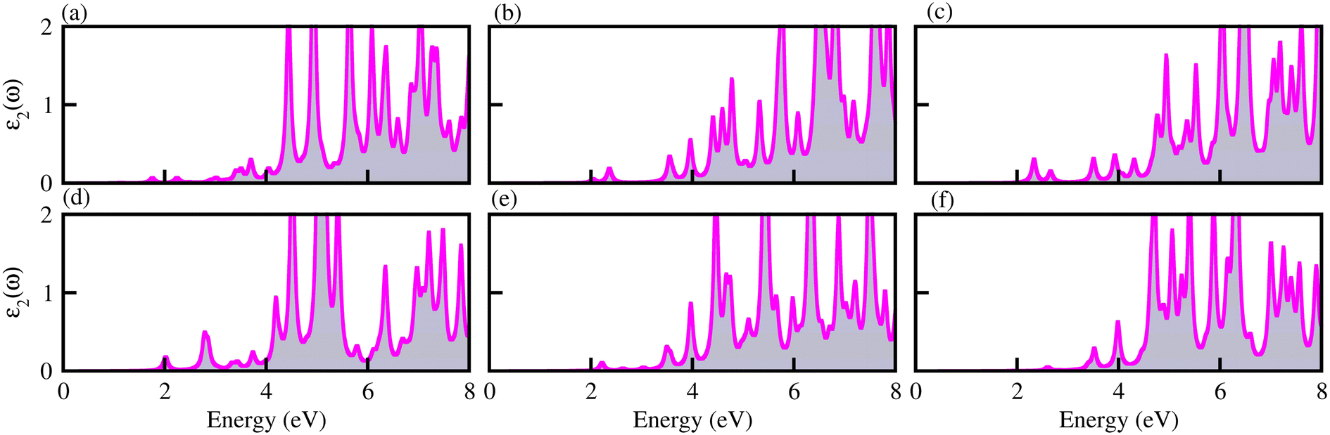 | ||
| Fig. 8 ε 2(ω) of (a) GaN-Ti2CO2, (b) GaN-Zr2CO2, (c) GaN-Hf2CO2, (d) AlN-Ti2CO2, (e) AlN-Zr2CO2 and (f) AlN-Hf2CO2 vdWHs. | ||
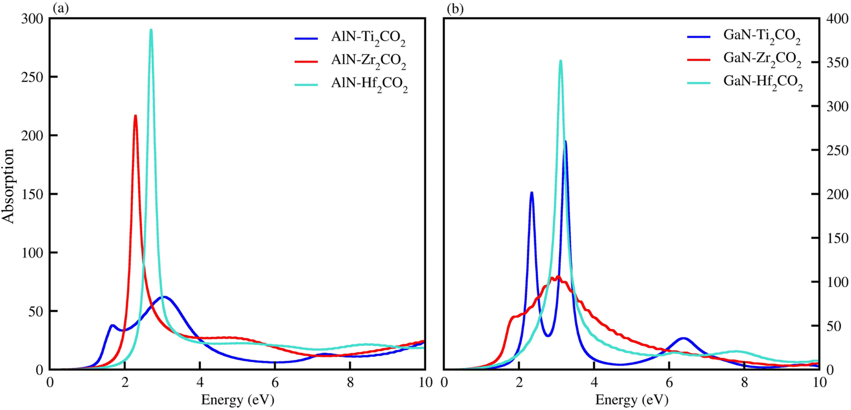 | ||
| Fig. 9 α(ω) of (a) AlN-Ti2CO2, AlN-Zr2CO2 and AlN-Hf2CO2 and (b) GaN-Ti2CO2, GaN-Zr2CO2, GaN-Hf2CO2, vdWHs. | ||
To utilize solar energy for environmentally friendly applications, it is necessary to design novel materials with visible light absorption. Therefore, to explore the ability of PN-M2CO2 (P = Al, Ga; M = Ti, Zr, Hf) vdWHs for water splitting, we calculated the photocatalytic properties by using Mullikan electronegativity.91–93 The conduction band (CB) and valence band (VB) edge position of the semiconductors are the two most important parameters to determine photocatalytic activity using under-stimulated sunlight irradiation.94 We denote it as H+/H2 for reduction and O2/H2O for oxidation, as shown in Fig. 10. If ECB is positioned more negatively than the energy of the H2/+ potential and the EVB is more positive than the energy of the O2/H2O potential, then water molecules can be easily split into H2 and O2.95 In GaN-Zr2CO2, GaN-Hf2CO2, AlN-Zr2CO2, and AlN-Hf2CO2, the ECB is positioned more negatively than the energy of the H2/H+ potential, and can split water into H2. Similarly, if the EVB is more positive than the energy of the O2/H2O potential, then the water molecule can easily split into O2. Similarly, GaN-Ti2CO2 and AlN-Ti2CO2 have the ability to produce O2 while ECB has a positive value and is unable to produce H2 due to the narrow bandgap nature. All these findings demonstrate that PN-M2CO2 (P = Al, Ga; M = Ti, Zr, Hf) vdWHs are the best candidates for photocatalytic water splitting and provide a guideline for designing high performance nanoelectronic, optoelectronic and photocatalytic device applications.
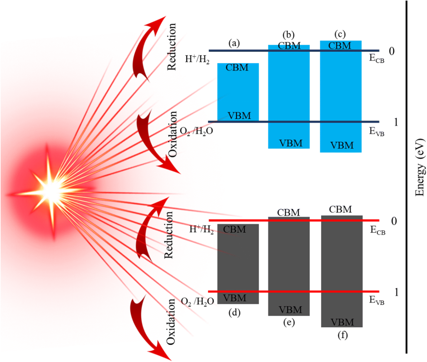 | ||
| Fig. 10 Band alignment for the valence band (VB) and conduction band (CB) edge of (a) GaN-Ti2CO2, (b) GaN-Zr2CO2, (c) GaN-Hf2CO2, (d) AlN-Ti2CO2, (e) AlN-Zr2CO2 and (f) AlN-Hf2CO2, vdWHs. | ||
IV. Conclusions
Using DFT, the calculated electronic band structure and photocatalytic performance of PN (P= Ga, Al) and M2CO2 (M = Ti, Zr, Hf) monolayers show the potential of such materials in photocatalytic applications. Based on the same hexagonal symmetry and experimentally achievable lattice mismatch of PN (P = Ga, Al) with M2CO2 (M = Ti, Zr, Hf) monolayers, we have fabricated PN-M2CO2 vdWHs. The thermal stability of PN-M2CO2 vdWHs are confirmed by calculating the binding energies, interlayer distance and AIMD, which demonstrate that these materials can easily be fabricated experimentally. All the PN-M2CO2 vdWHs are indirect bandgap semiconductors, while Type-II[-I] band alignment is obtained for GaN(AlN)-Ti2CO2[GaN(AlN)-Zr2CO2 and GaN(AlN)-Hf2CO2] vdWHs. The PN-Ti2CO2 (PN-Zr2CO2) vdWH, PN(Zr2CO2) monolayer, have greater potential than the Ti2CO2(PN) monolayer, indicating that charge is transferred from the Ti2CO2(PN) to PN(Zr2CO2) monolayer, hence, the potential drop at the interface separates charge carriers (electron and holes). The work function and effective mass of the carriers of PN-M2CO2 vdWHs are also calculated and presented. For the AlN-Ti2CO2 effective mass of electrons and holes is greater, and is hence suggested for logic devices, while for the rest of the vdWHs, the effective mass of electrons and holes are lower. Based on ε2(ω) α(ω), a red (blue) shift is observed in the position of excitonic peaks from AlN to GaN in PN-Ti2CO2 and PN-Hf2CO2 (PN-Zr2CO2) vdWHs, while a significant absorption for photon energies above 2 eV for AlN-Zr2CO2, GaN-Ti2CO2 and PN-Hf2CO2, make them candidates with a good optical profile. The calculated photocatalytic properties demonstrate that PN-M2CO2 (P = Al, Ga; M = Ti, Zr, Hf) vdWHs are the best candidates for photocatalytic water splitting and provide a guideline for experimentalist to design high performance nanoelectronics, optoelectronic and photocatalytic device applications.Conflicts of interest
There is no conflicts to declare.Acknowledgements
This research was funded by the Princess Nourah bint Abdulrahman University Researchers, Riyadh, Saudi Arabia, with supporting project number (PNURSP2023R71). The authors extend their sincere appreciation to Princess Nourah bint Abdulrahman University.References
- M. G. Walter, E. L. Warren, J. R. McKone, S. W. Boettcher, Q. Mi, E. A. Santori and N. S. Lewis, Chem. Rev., 2010, 110, 6446 CrossRef CAS PubMed.
- T. Hisatomi, J. Kubota and K. Domen, Chem. Soc. Rev., 2014, 43, 7520 RSC.
- K. Maeda and K. Domen, J. Phys. Chem. C, 2007, 111, 7851 CrossRef CAS.
- F. E. Osterloh, Chem. Mater., 2008, 20, 35 CrossRef CAS.
- B. Huang and J. N. Hart, Phys. Chem. Chem. Phys., 2020, 22, 1727 RSC.
- F. Schedin, A. K. Geim, S. V. Morozov, E. W. Hill, P. Blake, M. L. Katsnelson and K. S. Novoselov, Nat. Mater., 2007, 6, 652 CrossRef CAS PubMed.
- Y. Li, Y. L. Li, B. Sa and R. Ahuja, Catal. Sci. Technol., 2017, 7, 545 RSC.
- K. Xu, L. Wang, X. Xu, S. X. Dou, W. Hao and Y. Du, Energy Storage Mater., 2019, 19, 446 CrossRef.
- S. A. Khan, Phys. Chem. Cem. Phys., 2017, 19, 14738–14744 RSC.
- M. Khazaei, A. Ranjbar, M. Arai, T. Sasaki and S. Yunoki, J. Mater. Chem. C, 2017, 5, 2488 RSC.
- B. Fu, j. Sun, C. Wang, C. Shang, L. Xu, J. Li and H. Zhang, Small, 2021, 17, 2006054 CrossRef CAS PubMed.
- L. Wang, M. Han, C. E. Shuck, X. Wang and Y. Gogotsi, Nano Energy, 2021, 88, 106308 CrossRef CAS.
- H. Huang, R. Jiang, Y. Feng, H. Ouyang, N. Zhou, X. Zhang and Y. Wei, Nanoscale, 2020, 12, 1325 RSC.
- W. Wu, H. Fang, H. Ma, L. Wu, W. Zhang and H. Wang, Nano-Micro Lett., 2021, 13, 1 CAS.
- B. Ahmed, A. E. Ghazaly and J. Rosen, Adv. Funct. Mater., 2020, 30, 2000894 CrossRef CAS.
- X. Xu, Y. Zhang, H. Sun, J. Zhou, F. Yang, H. Li and Z. Peng, Adv. Electron. Mater., 2021, 7, 2000967 CrossRef CAS.
- F. Ming, H. Liang, G. Huang, Z. Bayhan and H. N. Alshareef, Adv. Mater., 2021, 33, 2004039 CrossRef CAS PubMed.
- W. Li, C. Zhuang, Y. Li, C. Gao, W. Jiang, Z. Sun and K. Qi, Ceram, 2021, 47(15), 21769 CAS.
- M. R. Lukatskaya, S. Kota, Z. Lin, M. Q. Zhao, N. Shpigel, M. D. Levi, J. Halim, P. L. Taberna, M. W. Barsoum and P. Simon, Nat. Energy, 2017, 2, 17105 CrossRef CAS.
- N. Zhou, R. Yang and T. Zhai, Mater. Today Nano, 2019, 8, 100051 CrossRef.
- Y. X. Chen, K. L. Liu, J. X. Liu, T. R. Lv, B. Wei, T. Zhang, M. Q. Zeng, Z. C. Wang and L. Fu, J. Am. Chem. Soc., 2018, 140(48), 16392 CrossRef CAS PubMed.
- X. Zhou, M. M. Wu, J. Zhou and Q. Sun, Appl. Phys. Lett., 2009, 94, 103105 CrossRef.
- Y. Li, Z. Zhou, P. Shen, S. B. Zhang and Z. Chen, Nanotechnology, 2009, 20, 215701 CrossRef PubMed.
- Z. Wang, G. Wang, X. Liu, S. Wang, T. Wang and L. Zhang, J. Mater. Chem. C, 2021, 9, 17201 RSC.
- Z. Y. Balushi, K. Wang, R. K. Ghosh, R. A. Vilá, S. M. Eichfeld and J. A. Robinson, Nat. Mater., 2016, 15, 1166 CrossRef PubMed.
- Y. Duan, L. Qin, L. Shi, G. Tang and H. Shi, Appl. Phys. Lett., 2012, 100, 022104 CrossRef.
- Z. Qin, G. Qin, X. Zuo, Z. Xiong and M. Hu, Nanoscale, 2017, 9, 4295 RSC.
- Q. Peng, X. J. Chen, S. Liu and S. De, RSC Adv., 2013, 3, 7083 RSC.
- H. Shu, X. Niu, X. Ding and Y. Wang, Appl. Surf. Sci., 2019, 479, 475 CrossRef CAS.
- C. Xu, L. Xue, C. Yin and G. Wang, Phys. Status Solidi A, 2003, 198, 329 CrossRef CAS.
- S. Hersee, X. Sun and X. Wang, Nano Lett., 2006, 6, 1808 CrossRef CAS PubMed.
- X. Zhang, Z. Liu and S. Hark, Solid State Commun., 2007, 143, 317 CrossRef CAS.
- B. Liu, W. Yang, J. Li, X. Zhang, P. Niu and X. Jiang, Nano Lett., 2017, 17, 3195 CrossRef CAS PubMed.
- C. W. Zhang, J. Appl. Phys., 2012, 111, 043702 CrossRef.
- S. Bhattacharya, A. Datta, S. Dhara and D. Chakravorty, J. Raman Spectrosc., 2011, 42, 429 CrossRef CAS.
- A. K. Geim and I. V. Grigorieva, Nature, 2013, 499, 419 CrossRef CAS PubMed.
- K. S. Novoselov, O. A. Mishchenko, O. A. Carvalho and A. H. Castro Neto, Science, 2016, 353, 9439 CrossRef PubMed.
- Q. Peng, C. Si, J. Zhou and Z. Sun, Appl. Surf. Sci., 2019, 480, 199 CrossRef CAS.
- L. Jiao, C. Zhang, C. Geng, S. Wu, H. Li, W. Lv, Y. Tao, Z. Chen, G. Zhou, J. Li and G. Ling, Adv. Energy Mater., 2019, 9, 1900219 CrossRef.
- M. Q. Zhao, N. Trainor, C. E. Ren, M. Torelli, B. Anasori and Y. Gogotsi, Adv. Mater. Technol., 2019, 4, 1800639 CrossRef.
- X. Shen, X. Huang, H. Wang and H. Zhan, Solid State Commun., 2022, 346, 114720 CrossRef CAS.
- A. Abid, M. Idrees, H. U. Din, Q. Alam, B. Amin and M. Haneef, Mater. Today Commun., 2021, 26, 101702 CrossRef CAS.
- M. Munawar, M. Idrees, I. Ahmad, H. U. Din and B. Amin, RSC Adv., 2022, 12, 42 RSC.
- H. P. Lee, J. Perozek, L. D. Rosario and C. Bayram, Sci. Rep., 2016, 6(1), 1–10 CrossRef PubMed.
- R. Sivasamy, K. Paredes-Gil and F. Quero, Phys. E., 2022, 135, 114994 CrossRef CAS.
- X. Wang, G. Fabi, R. Chaudhuri, A. Hickman, M. J. Asadi, K. Nomoto and J. C. Hwang, Appl. Phys. Lett., 2022, 120, 012103 CrossRef CAS.
- H. Shu, Mater. Sci. Eng., B, 2020, 261, 114672 CrossRef CAS.
- G. Wang, W. Tang, L. Geng, Y. Li, B. Wang, J. Chang and H. Yuan, Phys. Status Solidi B, 2020, 257(3), 1900663 CrossRef CAS.
- X. Liu, Z. Zhang, Z. Luo, B. Lv and Z. Ding, Nanomaterials, 2019, 9, 1674 CrossRef CAS PubMed.
- L. Meng, Q. Huang, C. Liu, H. Li, W. Yan, Q. Zhao and X. Yan, Chem. Phys. Lett., 2021, 781, 138989 CrossRef CAS.
- R. Zhang, Y. Zhang, X. Wei, T. Guo, J. Fan and L. Duan, Appl. Surf. Sci., 2020, 528, 146782 CrossRef CAS.
- M. Zhang, R. Si, X. Wu, Y. Dong, K. Fu, X. Xu and Y. Guo, J. Mater. Sci.: Mater. Electron., 2021, 32(14), 19368–19379 CrossRef CAS.
- K. Ren, R. Zheng, P. Xu, D. Cheng, W. Huo, J. Yu and Q. Sun, Nanomaterials, 2021, 11(9), 2236 CrossRef CAS PubMed.
- I. Shahid, S. Ahmad, N. Shehzad, S. Yao, C. V. Nguyen, L. Zhang and Z. Zhou, Appl. Surf. Sci., 2020, 523, 146483 CrossRef CAS.
- X. Zhang, A. Chen, Z. Zhang, M. Jiao and Z. Zhou, Nanoscale Adv., 2019, 1, 154–161 RSC.
- X. Zhang, Z. Zhang, D. Wu, X. Zhang, X. Zhao and Z. Zhou, Small Methods, 2018, 2, 1700359 CrossRef.
- W. Kohn and L. J. Sham, Phys. Rev., 1965, 140, A1133 CrossRef.
- G. Kresse and J. Hafner, Phys. Rev. B: Condens. Matter, 1993, 47, 558 CrossRef CAS PubMed.
- J. P. Perdew, K. Burke and M. Ernzerhof, Phys. Rev. Lett., 1996, 77, 3865 CrossRef CAS PubMed.
- J. Heyd, G. E. Scuseria and M. Ernzerhof, J. Chem. Phys., 2006, 124, 219906 CrossRef.
- R. Yuan, J. A. Napoli, C. Yan, O. Marsalek, T. E. Markland and M. D. Fayer, ACS Cent. Sci., 2019, 5, 1269 CrossRef CAS PubMed.
- N. Khossossi, Y. Benhouria, S. R. Naqvi, P. K. Panda, I. Essaoudi, A. Ainane and R. Ahuja, Energy Fuels, 2020, 4(9), 4538 CAS.
- X. Jiang, P. Wang and J. Zhao, J. Mater. Chem. A, 2015, 3(15), 7750 RSC.
- X. Leng, F. Jin, M. Wei and Y. Ma, Wiley Interdiscip. Rev.: Comput. Mol. Sci., 2016, 6(5), 532–550 CAS.
- J. Pešić and R. Gajić, Opt. Quantum Electron., 2016, 48, 1–7 CrossRef.
- P. Giannozzi, S. Baroni, N. Bonini, M. Calandra, R. Car, C. Cavazzoni, D. Ceresoli, G. L. Chiarotti, M. Cococcioni, I. Dabo, A. D. Corso, S. D. Gironcoli, S. Fabris, G. Fratesi, R. Gebauer, U. Gerstmann, C. Gougoussis, A. Kokalj, M. Lazzeri, L. M. Samos, N. Marzari, F. Mauri, R. Mazzarello, S. Paolini, A. Pasquarello, L. Paulatto, C. Sbraccia, S. Scandolo, G. Sclauzero, A. P. Seitsonen, A. Smogunov, P. Umari and R. M. Wentzcovitch, J. Phys.: Condens. Matter, 2009, 21, 395502 CrossRef PubMed.
- S. Y. Vaselnia, M. K. Aminian and H. Motahari, J. Phys. Chem. Solids, 2020, 138, 109244 CrossRef CAS.
- M. A. Marques and E. K. Gross, Annu. Rev. Phys. Chem., 2004, 55, 427–455 CrossRef CAS PubMed.
- K. Ren, S. Wang, Y. Luo, J. P. Chou, J. Yu, W. Tang and M. Sun, J. Phys. D: Appl. Phys., 2020, 53, 185504 CrossRef CAS.
- M. Liao, P. Nicolini, L. Du, J. Yuan, S. Wang, H. Yu, J. Tang, P. Cheng, K. Watanabe, T. Taniguchi, L. Gu, V. Claerbout, A. Silva, D. Kramer, T. Polcar, R. Yang, D. Shi and G. Zhang, Nat. Mater., 2022, 21, 47 CrossRef CAS PubMed.
- B. Bhattacharya and U. Sarkar, Chem. Phys., 2016, 478, 73 CrossRef CAS.
- N. Kharche, Y. Zhou, K. P. OBrien, S. Kar and S. K. Nayak, ACS Nano, 2011, 5, 6096 CrossRef CAS PubMed.
- H. U. Din, M. Idrees, A. Albar, M. Shafiq, I. Ahmad, C. V. Nguyen and B. Amin, Phys. Rev. B, 2019, 100, 165425 CrossRef CAS.
- F. Tran and P. Blaha, Phys. Rev. Lett., 2009, 102, 226401 CrossRef PubMed.
- Q. Wang and K. Domen, Chem. Rev., 2020, 120, 919–985 CrossRef CAS PubMed.
- V. D. Ganesan, J. Linghu, C. Zhang, Y. P. Feng and L. Shen, Appl. Phys. Lett., 2016, 108, 122105 CrossRef.
- M. Tangi, P. Mishra, M.-Y. Li, M. K. Shakfa, D. H. Anjum, M. N. Hedhili, T. K. Ng, L.-J. Li and B. S. Ooi, Appl. Phys. Lett., 2017, 111, 092104 CrossRef.
- J. Meng, J. Wang, Q. Li and J. Yang, J. Mater. Chem. A, 2022, 10, 3443 RSC.
- J. Hwang, A. J. Martin, J. M. Millunchick and J. D. Phillips, J. Appl. Phys., 2012, 111, 074514 CrossRef.
- M. Z. Bellus, M. Li, S. D. Lane, F. Ceballos, Q. Cui, X. C. Zengand and H. Zhao, Nanoscale Horiz., 2017, 2, 31 RSC.
- X. H. Li, B. J. Wang, G. D. Wang, X. F. Yang, R. Q. Zhao and H. S. Ke, Sustainable Energy Fuels, 2021, 5(8), 2249 RSC.
- M. Idrees, C. N. Nguyen, H. D. Bui, I. Ahmad and B. Amin, Phys. Chem. Chem. Phys., 2020, 22(36), 20704 RSC.
- X. Li, F. Jia, J. Du, X. Song, C. Xia, Z. Wei and J. Li, J. Mater. Chem. C, 2018, 6(37), 10010 RSC.
- Y. Liu, X. Duan, H. J. Shin, S. Park, Y. Huang and X. Duan, Nature, 2021, 591, 43 CrossRef CAS PubMed.
- Y. Liu, X. Duan, Y. Huang and X. Duan, Chem. Soc. Rev., 2018, 47, 6388 RSC.
- F. Bassani, G. P. Parravicini, R. A. Ballinger and J. L. Birman, Phys. Today, 1976, 29(3), 58c CrossRef.
- M. Barhoumi, I. Said, N. Sfina, N. K. Al Saleem and T. Ghrib, Mater. Chem. Phys., 2022, 286, 126158 CrossRef CAS.
- M. Fox, Optical Properties of Solids, Oxford University Press, 2001 Search PubMed.
- I. Timrov, N. Vast, R. Gebauer and S. Baroni, Comput. Phys. Commun., 2015, 196, 460 CrossRef CAS.
- M. D. Scafetta, A. M. Cordi, J. M. Rondinelli and S. J. May, J. Phys.: Condens. Matter, 2014, 26, 505502 CrossRef PubMed.
- M. J. Fang, C. W. Tsao and Y. J. Hsu, J. Phys. D: Appl. Phys., 2020, 53, 143001 CrossRef CAS.
- J. J. Liu, X. L. Fu, S. F. Chen and Y. F. Zhu, Appl. Phys. Lett., 2011, 99, 191903 CrossRef.
- H. L. Zhuang and R. G. Hennig, Phys. Rev. B: Condens. Matter Mater. Phys., 2013, 88, 115314 CrossRef.
- M. J. Islam, D. A. Reddy, J. Choi and T. K. Kim, RSC Adv., 2016, 6, 19341 RSC.
- M. Idrees, C. Nguyen, H. Bui, I. Ahmad and B. Amin, Phys. Chem. Chem. Phys., 2020, 22, 20704 RSC.
| This journal is © The Royal Society of Chemistry 2023 |