
 Open Access Article
 This Open Access Article is licensed under a
 Creative Commons Attribution 3.0 Unported Licence
Epitaxial growth of crystal phase quantum dots in III–V semiconductor nanowires
Miguel Sinusia
Lozano
 and
Víctor J.
Gómez
*
and
Víctor J.
Gómez
*
Nanophotonics Technology Center, Universitat Politècnica de València, Camino de Vera, s/n Building 8F, 2a Floor, 46022 Valencia, Spain. E-mail: vjgomher@ntc.upv.es
First published on 6th March 2023
Abstract
Crystal phase quantum dots (QDs) are formed during the axial growth of III–V semiconductor nanowires (NWs) by stacking different crystal phases of the same material. In III–V semiconductor NWs, both zinc blende (ZB) and wurtzite (WZ) crystal phases can coexist. The band structure difference between both crystal phases can lead to quantum confinement. Thanks to the precise control in III–V semiconductor NW growth conditions and the deep knowledge on the epitaxial growth mechanisms, it is nowadays possible to control, down to the atomic level, the switching between crystal phases in NWs forming the so-called crystal phase NW-based QDs (NWQDs). The shape and size of the NW bridge the gap between QDs and the macroscopic world. This review is focused on crystal phase NWQDs based on III–V NWs obtained by the bottom-up vapor–liquid–solid (VLS) method and their optical and electronic properties. Crystal phase switching can be achieved in the axial direction. In contrast, in the core/shell growth, the difference in surface energies between different polytypes can enable selective shell growth. One reason for the very intense research in this field is motivated by their excellent optical and electronic properties both appealing for applications in nanophotonics and quantum technologies.
 Miguel Sinusia Lozano | Miguel Sinusia Lozano got his Bachelor and Master’s degree in Materials Science and Engineering in 2014 and 2016 respecively from the Universidad Politécnica de Madrid. In 2020 he graduated from the Universidad Politécnica de Madrid where he pursued his PhD focusing on the piezoelectric ScAlN compound and its usage in surface acoustic wave (SAW) devices. He is currently working at the Nanophotonics Technology Center (NTC), Universitat Politècnica de València. His work is devoted to the study of III–V semiconductors for sensing and quantum-related technologies. |
 Víctor J. Gómez | Víctor Jesús Gómez Hernández joined the Nanophotonics Technology Center, Universitat Politècnica de València, as a Distinguished Researcher where he leads the III–V semiconductors and graphene group. He received his PhD at Universidad Politécnica de Madrid in 2017 and did 2 postdocs at Cardiff and Lund University for a total of 3 years. Dr Víctor J. Gómez main scientific goal is to develop new material architectures through high-level scientific research. Víctor has already participated in interdisciplinary and international projects, for a total of 13 different projects, 5 of them as Principal Investigator (∼1 M€) and leads two infrastructure projects (>3 M€). |
1. Introduction
This review is focused on crystal phase QDs formed in III–V semiconductor NWs by stacking, in the axial direction, WZ or ZB crystal phases of the same material by the bottom-up VLS growth method. General concepts of WZ and ZB polytypes will first be introduced. Then, the growth mechanism and control over the nucleation, layer growth, and crystal phase selection will be reviewed together with the process of selective core/shell growth. Following this, the review will cover the optical and electronic properties including specific examples and case studies.Nanoscale structures, such as NWs, enable heterostructures to overcome the limitations related to lattice mismatch and strain relief, whereas the growth of their planar counterparts is strongly constrained to a small lattice parameter window, therefore, offering additional degrees of freedom, for example in terms of materials combination, for the formation of low dimensional heterostructures, including quantum wells (QW), quantum wires (QWRs), and QDs embedded in NWs, also known as nanowire quantum dots (NWQDs). The three-dimensional carrier confinement and localized/discrete carrier states in QDs are predicted1 to introduce new physical phenomena to diode lasers and other photonic devices. Traditionally NWQDs can be produced via heterostructured interfaces between materials with different band gaps (i.e. switching materials and/or alloy composition) or by changing the crystal structure without changing the material. Epitaxially grown NWs with embedded QDs offer a way for fully deterministic positioning of the QDs. Moreover, the shape and aspect ratio of the NWs guarantee the link of the QD with the macroscopic world, either by electrical contacts or photon emission.
The combination of NWs and QDs is crucial for photonics due to the enhanced spontaneous emission rate by coupling generated light with cavity modes (Purcell effect), waveguiding, and suppression of the total internal reflection so that the efficiency of light extraction can theoretically approach 100%.2–6 Additionally, the directionality of emissions can be controlled by engineering the shape of the tip of the NW,.7 thus resulting in the realization of novel nanophotonic devices based on nanowires. In agreement with this, NWQD-based single-photon subwavelength detectors8,9 and emitters10,11 have been demonstrated. NWQDs can also easily be addressed via electrical contacts. Therefore, QDs can be electrically pumped when embedded in an NW axial p–n junction. This allows the injection of electron–hole pairs and their subsequent radiative recombination into photons emitted by the QD.12 In addition, virtual QDs can be induced by localized electrical gating, allowing a versatile manipulation of the density of states in the QD.13,14 In this case, the QD-like confinement is achieved by local tuning of the Fermi level by applying the right voltage by means of precisely positioned gate electrodes instead of engineering the QD by a local difference either in material, composition or crystal phase.
Two different approaches can be distinguished for the fabrication of NWQDs: top-down and bottom-up.
1.1 Top-down fabrication of NWQDs
The top-down approach involves the breaking down of a substrate including QDs into nanostructures such us NWs. By using this fabrication method precisely positioned one-dimensional structures can be obtained. Depending on the density of QDs in the substrate and the NW diameter (defined via lithography), the resulting NWQDs can embed one or several QDs.15–17 One of the main drawbacks of this approach is the impact of etching on exposed surfaces, also referred to as etch damage, hindering the material quality and the subsequent device performance. Moreover, as this approach needs a substrate containing QDs, this technique is limited to materials and material combinations which already exist in bulk, which is not generally the case for different crystal phases.In general, self-assembled semiconductor QDs are grown in the Stranski–Krastanov (SK) growth mode. The SK growth mode is driven by the lattice mismatch between the substrate and the growing layer. After growing a few monolayers (wetting layer), the accumulated strain is relieved via the random nucleation and growth of island-like formation (QDs).18 The resulting QDs can then be embedded in the material after the epitaxial growth of a new epi-layer called the capping layer. The optical properties of the QDs depend on the composition (in the case of ternary or quaternary alloys), size, and strain. It is worth highlighting that the composition of the alloy defines the lattice parameter, which is related to the strain and, therefore, to the size of the QDs. Moreover, the emission energy of the QDs is directly related to the surrounding material (wetting and capping layers), determining the charge carrier confinement in the QD. One of the main drawbacks of self-assembled QDs is the lack of uniformity in heights and lateral size, ranging typically between 1–10 and 10–70 nm respectively.19 The density and size distribution can be controlled up to some extent by varying the growth conditions.20 Another disadvantage is the material inter-mixing between the QD and capping layer that can take place during the growth, which further increases the variation in the optical properties of the QDs.21 Therefore, the top-down approach must deal with QDs ensembles with limited control in location, size, density, and material uniformity.
1.2 Bottom-up fabrication of NWQDs
However, in the bottom-up approach chemical or physical forces operating at the nanoscale during the growth process are employed to assemble the NWs where the QDs are included. This can be achieved by changing the growth conditions, precursor species or precursor flows. The bottom-up approach offers a way to grow NWQDs with smooth sidewalls with axial and/or radial heterostructures or doping profiles. Due to the nanowire geometry, lattice mismatch and the resulting stress can be accommodated via strain relaxation in the radial direction without the introduction of defects, i.e., dislocations. This allows us to obtain NWQDs in both the axial and radial directions.22–24 An additional advantage of NWQDs to be considered is their relatively high surface-to-volume ratio compared to their planar counterparts that allows the existence of other crystal phases not stable in the bulk (polytypism).25–27 In III–V NWs, ZB and WZ alternating segments can be successfully controlled to confine charges and obtain type-II NWQDs within the same material.28–31The bottom-up NW growth approach relies either on the VLS (Fig. 1A) or on the selective-area epitaxy (SAE, Fig. 1B). It is worth mentioning that the main difference between the two growth modes is in the axial direction, being the radial growth dominated by the vapor–solid growth mode which is similar in both cases. Both growth modes, VLS or SAE, allow forming NWQDs. Compared to the top-down fabrication, there are some major advantages when using the bottom-up growth of NWQDs: a wider material compatibility, deterministic fabrication down to a single QD per NW, and natural alignment of the QD along the NW axis.
 | ||
| Fig. 1 Schematic representation of the NW growth modes. (A) VLS growth mode where the axial growth is catalysed by a metallic droplet (typically Au). (B) SAE growth mode where the growth takes place at an opening in a mask layer. | ||
The VLS NW growth mode,32 originally introduced by Wagner and Ellis in 1964,33 is mediated by a metallic droplet in the liquid phase, which collects the growth species introduced in the reactor chamber in the vapor phase, leading to the nucleation of the crystal in the solid phase, below the droplet. Then, the growing NW lifts the droplet that remains at the tip of the NW. In 1991, Hiruma and co-workers34 grew, for the first time, III–V compound nanowires. One year later, in 1992, the same group reported the co-existence of both ZB and WZ crystal structures in indium arsenide NWs.35 In 1994, Murayama and co-workers reported the calculations of the band offsets at WZ–ZB interfaces.36 However, it was not until 2008 that the first successful attempts to control the crystal structure during NW growth37,38 and the first optical studies39–42 were reported. This progress practically enables engineering of the electronic structure of a single material. For instance, a WZ/ZB/WZ structure can define a quantum well in a single material. Growing such a structure in a NW will also confine charges in two other dimensions, forming a crystal phase NWQD. During the past few decades, a huge effort has been made in order to understand the VLS growth process, thus leading to NWs with high crystal quality,43 controlled crystal phase,27,44 controlled axial doping,45 and to obtain axial and radial heterostructures.22,46,47 Despite the significant progress made, the detailed growth mechanism is not fully understood yet and research in this area is going on.
The metallic droplet material can either be one of the group-III growth species (leading to a self-catalysed or self-assisted growth) or a foreign material, being Au the most widespread and studied.48 The metallic droplets, catalysts, can be randomly deposited on the substrate by means of spark discharge,49 aerosol generation,50 or annealing of Au thin films.51 Additionally, the NW growth sites can be lithographically defined showing the upscaling possibilities of this technology.52–55
Since metal contamination from the metallic droplet in the NWQD could be detrimental to its optical and electrical properties, self-catalysed or catalyst-free growth methods have been developed.56–58 Also in this case, arrays of NWs can be grown on a lithographically patterned substrate.58 The SAE is a catalyst-free direct vapor–solid growth and is based on growth mask layers with openings that define the NW growth. The growth is driven by differences in the nucleation and crystal growth on different crystal facets mainly due to differences in surface energies.59 The openings in the growth mask expose the underlying substrate and define the locations where the epitaxy of the NWs starts. For the axial growth along the 〈111〉 direction, the conditions are chosen such that the {110} facets have significantly lower growth rates than the {111} facets. Then, the NW grows with {110} lateral facets and the NW shows a hexagonal cross-section. Under the appropriate conditions, the radial growth can be fully suppressed, and the NW diameter remains equal to the mask opening. Fig. 1B shows the schematic representation of the SAE growth.
As with VLS growth, it is possible to obtain high crystal quality,60 control the crystal phase,61 switch between axial and radial growth,62 dope the NW during growth,62 and obtain axial and radial heterostructures.62,63 In principle, SAE growth is less complex than VLS growth, as only two phases, vapor and solid, are involved. Nevertheless, the growth dynamics are highly complex, for example the dependence on the diameter of the mask openings and distance between openings, on the NW geometry, and on the relative supply of group III (or V) constituents in the growth of ternaries.64–66 Therefore, the main challenges in the SAE growth method are to obtain a high degree of control in NW growth and in understanding its subtleties.
In general, NWs and NWQDs can be grown by different techniques ranging from metal–organic vapor-phase epitaxy (MOVPE),2,28,67 to chemical beam epitaxy (CBE),68 and molecular beam epitaxy (MBE).56,69 Moreover, NWs and NWQDs can be in situ characterized by transmission electron microscopy during growth by either MOVPE70,71 or MBE.57 Furthermore, crystal phase heterostructures can be exploited not only with NWs, but also with nano-membranes72,73 and microdisks.74 The area of NWQDs is extremely broad with application examples in several fields such as quantum technologies75,76 and nanophotonics.77,78
2. Crystal phase axial NWQDs
The idea behind the growth of NWQDs is relatively simple: a material with a lower band gap should be inserted inside another material with a higher band gap. Thus, forming an axial structure of the style A/B/A, where B shows quantum confinement due to the differences in band gap energy and the relative position of the band edges. The stacking sequence is obtained typically by changing the growth precursors during the axial NW growth. The patterning of the catalysts in VLS controls the position of the nanowire, and the diameter of the catalyst defines the NW and QD diameters. The axial position of the QD and its length are defined by the growth time. Therefore, the combination of patterning together with the VLS bottom-up growth offer full control over the size and position of the QD inside the NW and on the substrate. Moreover, radial growth can be employed either to fully embed the QD inside the NW or to grow an oxide shell, using atomic layer deposition (ALD), to improve the waveguiding properties of the NW.79 Another advantage of axial NWQDs arises when the NW diameter is properly chosen. This way, the emission from the QD can be efficiently coupled to the fundamental waveguiding mode of the NW, thus enhancing the extraction efficiency. Nowadays, this is possible thanks to a deep understanding and control of the growth process. In addition, axial NWQDs can be electrically injected when contacting the region above and below the QD. In this case, electrons, and holes flow from the top region to the bottom one going through the QD region defined in between.2.1 Material composition vs. crystal phase QDs
The axial growth of III–V NWQDs relies on the possibility to change the material composition or crystal phase during growth. Two approaches can be differentiated to realize NWQDs. First, by heterostructuring semiconductor materials with different band gaps, or second, by tuning the crystal phase of a single material. For the first approach, the perfection of the NWQD is limited by the difficulty to control the interface abruptness and material composition at the atomic level80–82 which unfortunately are determining factors for the physical properties of QDs as they define the shape of the potential well.29,83 Recent studies have shown that perfect atomically sharp interfaces can be achieved if the crystal structure is changed instead of the material composition28,29,84 and the crystal structure can be controlled using basic growth parameters43,44 creating crystal phase QDs, which, in some aspects, supersede material QDs. As the interfaces are defined between different crystal phases in the same material, no atom intermixing can occur, creating atomically sharp WZ–ZB interfaces.28,85 Moreover, there is minimal strain at a WZ–ZB interface.86 This makes polytype heterostructures ideal candidates for the exploration of the low dimensionality properties of NWQDs. In addition, single electron transport83 and quantum light sources have been demonstrated using crystal phase NWQDs.87Regardless of the specific growth technique employed (MBE, MOCVD, Au-assisted, self-catalysed…), the way to define a crystal phase NWQD depends on the band alignment between WZ and ZB phases, and this is specific to a particular material. For example, in the case of InP, GaAs, and InAs there is a type-II band alignment between WZ and ZB,88 thus leading to the confinement of electrons in the ZB phase when it is sandwiched between WZ barriers. Moreover, these type-II structures can support the formation of indirect excitons at the interfaces between crystal phases (Fig. 4). Finally, the main limitation of the crystal phase approach is the lack of flexibility in the formation of QDs and the fixed and relatively small band offsets. Moreover, there are materials where it is not possible to form crystal phase QDs in a controlled way. This is the case of III-nitrides.
2.2 Crystal phases: zinc blende and wurtzite
Before describing the axial growth of crystal phase NWQDs, it is necessary to fully describe the crystal structures to be investigated: ZB and WZ. Both crystal phases differ only in their stacking sequence in the close-packed directions (〈111〉 in ZB and 〈0001〉 in WZ), as is shown in the top part of Fig. 2. Both structures consist of hexagonally close-packed planes of III–V pairs. The difference lies in the alignment of these hexagonally close-packed planes with their surrounding planes. For ZB, three sequential layers form a repeating unit (…ABCABCABC…), where each letter represents one of the three allowed positions of the pairs of group-III and group-V atomic layers along the specific 〈111〉 direction. For the WZ crystal phase, only two of the allowed positions are occupied, giving the stacking sequence …ABABAB… Otherwise, each atomic layer can be denoted separately, differentiating the two different atomic species, using lower-case and upper-case letters. Then the ZB and WZ stacking sequences can be written as …AaBbCcAaBbCc… and …AaBbAaBb…, respectively (see the bottom part of Fig. 2). When there is an intermixing of crystal structures and/or different faults appear in their stacking sequence, this notation becomes mandatory to fully describe and distinguish between different defects and stacking faults in the sequence of these two types of crystal structures.89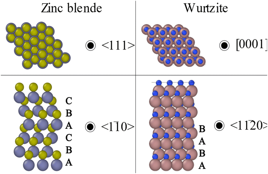 | ||
| Fig. 2 The atomic arrangement for the ZB and WZ structures. | ||
In III–V semiconductor NWs, the most frequently reported defects are twin planes, stacking faults, and the lack of control over the WZ and ZB formation. For the discussion on how to control the crystal phase, the reader is referred to Section 2.4.2. In general, twin planes and stacking fault defects have a negative impact on the optical and electronic properties of III–V semiconductor NWs by reducing the carrier lifetime, mobility, and quantum efficiency.90 On the other hand, stacking faults can have a positive impact on some of the physical properties of NWs as in the case of the field emission properties of GaN NWs.91,92 It has also been reported that there is an increase in Young's modulus with the increase in stacking faults for GaAs NWs.93 Twin planes are commonly observed in the ZB crystal phase. There, the stacking sequence is often found to unexpectedly change from an …ABCABCABC… stacking sequence to an …ABCACBACBA… The stacking sequence still corresponds to the ZB-type sequence after ‘A’, but before and after this bilayer the sequences are mirrored in ‘A’. This ‘mirror’ plane (A) is known as a twin plane and the sequences above and below the mirror plane have different twin orientations (Fig. 3). Nevertheless, the small part of the sequence surrounding the twin plane (…ABCACBACBA…) can be regarded as a WZ-type stacking sequence. In this review, we will follow the criteria published by Dick and co-workers89 where they exclusively use the terms twin and twin plane for this type of defect or interruption in the stacking sequence. They use WZ only when the WZ-type stacking sequence happens over at least four bilayers. Moreover, the term stacking faults refer to interruptions in the WZ stacking sequence such as …ABABCBABA… where C is the erroneous bilayer creating the stacking fault. Different strategies have been implemented to successfully reduce the density of stacking faults. Controlling the growth temperature and V/III ratio,38,43 NW diameter94 or the use of growth interruption strategies95 has been demonstrated to be critical in reducing the density of stacking defects.
 | ||
| Fig. 3 (a) Two different twin orientations of the ZB stacking sequence, denoted as ‘I’ and ‘II’. (b) When the two twin orientations of ZB are combined, the common plane A is a twin plane or twin plane. (c) Transmission electron microscopy image of a section of an InAs nanowire exhibiting two different orientations of zinc blende stacking (twin segments), separated by a twin plane. In the TEM image, group III and V atoms in adjacent planes cannot be resolved and appear as a single dot. Fig. 2 from Kimberly A Dick et al., 2010, Semicond. Sci. Technol., 25, 024009, reproduced with the permission of IOP Publishing. | ||
The different stacking sequences for ZB and WZ slightly change the local environment for each atom in the crystal lattice. In particular, the third-nearest-neighbour spacing is shorter in WZ. The shift in cohesive energy ranges from around −45 meV per III–V pair for AlN96 to around 25 meV for GaSb.97 This difference in bulk cohesive energy between the two phases is the reason why WZ is the preferred crystal structure for III-nitrides and, for example, WZ GaAs is not stable in bulk. Moreover, ZB and WZ crystal structures also have different surface terminations, as shown on the right-hand side of Fig. 2. In particular, for NWs growing in the 〈111〉/〈0001〉 directions, the surfaces present in the sidewalls of the NWs are different for the two structures.98,99 Although there is a wide dispersion in the estimates of what the actual energies of these surfaces are, most of the reports agree that the WZ {1010} surface should have a lower surface energy than the ZB {110}.98–101
2.3 The role of supersaturation
Supersaturation is a state of thermodynamic instability and hence the system becomes prone to reduce the supersaturation through the process called precipitation. Therefore, supersaturation is the driving force of the epitaxial growth process. Supersaturation can be defined as the difference in chemical potential between the growth environment and the substrate.| Δμ = μgas − μsubs | (1) |
At equilibrium, there is no difference between the chemical potential, the growth environment, and the chemical potential of the substrate. Therefore, Δμ = 0. To achieve crystal growth, a supersaturated growth environment is required. Crystal growth continues as long as the chemical potential of the growth environment is higher than that of the substrate. When the chemical potential of the substrate is higher than that of the growing environment, then the etching of the substrate is promoted over crystal growth.
For NWs in the VLS mode, growth occurs at the interface between the catalyst and NW, so this discussion will be focused on the chemical potential difference between the interface and the supply atoms. Supersaturation is affected by the growth temperature, pressure, and concentration of the growth species at the catalyst–NW interface. The concentration of growth species is directly controlled by the partial pressures of the precursors. However, it is vital to highlight that supersaturation is affected by many other growth parameters. As mentioned before, it depends on growth temperature and pressure. In general, the chemical potential difference between a vapour and its solid phase will decrease with temperature. However, for growth techniques that involve molecular precursors, such as MOVPE, the precursor decomposition rate depends exponentially on temperature, which increases the supersaturation for fixed precursor molar fractions. Moreover, surface reconstruction of the substrate varies with temperature and vapour molar fractions and directly affects the surface diffusion of adatoms. Therefore, the dependence of the supersaturation on the growth parameters is highly complex. NW systems are even more complicated. For example, when growth is diffusion limited, i.e., when the density of the NWs is high compared to the supply material, NWs compete for the supply material and the supersaturation per nanowire is therefore reduced. Supersaturation decreases as the NW grows away from the substrate, reducing the amount of material reaching the metallic particle, as reported for InP NWs.102 Other factors may include the local variation in precursor decomposition rate, solubility of the seed particle (which can be varied with temperature), trace impurities, and dopants in the system (which may affect adsorption, diffusion, and dissolution kinetics).
For III–V semiconductors, the group III and V elements, two different species, must combine to form the growing NW. These two species follow different, not always independent, kinetic processes. Both species have different adsorption, diffusion, and desorption rates, affecting their individual supersaturations at the catalyst–NW interface. When molecular precursor species are used, another degree of complexity is added to the system. This is because the two different precursor molecules will have to decompose first to deliver the atomic species to the growth front at a different decomposition rate. In addition, precursor molecules may compete for reactants, or react with each other at the surface or in the gas phase generating undesired by-products. Determining the optimum ratio of precursor molar fractions required to obtain equal adatom concentrations of the two species at the catalyst–NW interface is not straightforward. Therefore, the molar fraction ratio between the two species (V/III ratio) is an important parameter for the optimum NW growth.
2.4 Nanowire growth
The crystal phase sequence in the area surrounding the QD is of the style A/B/A, where crystal phase B shows quantum confinement. In the VLS method, the material forming the NW is dissolved in the metal droplet and, when reaching supersaturation, precipitates at the droplet–NW (liquid–solid) interface. Layer by layer, generating the longitudinal growth of the NW. However, multilayer growth has also been demonstrated.103 After a certain growth time and for a chosen NW length, the growth conditions are changed to switch to crystal phase B. Note that the growth rate may change. At the desired length of the segment of crystal phase B, the growth conditions are changed to switch back to crystal phase A. Eventually, the growth is stopped, and the result is a NW of a single material containing a crystal phase QD of the style A/B/A. Fig. 4 illustrates an example of crystal phase NWQD in InAs of the style WZ/ZB/WZ. If the dimensions of the lower band gap crystal phase are small enough, the corresponding segment should show quantum confinement and behave like a QD. | ||
| Fig. 4 (A) High-resolution transmission electron micrograph of an InAs NW with a ZB QD sandwiched between WZ barriers. (B) Schematic representation of the crystal structure stacking sequence and the resulting type-II band alignment. Adapted from Fig. 1 by Potts, H., Chen, I., Tsintzis, A. et al., Electrical control of spins and giant g-factors in ring-like coupled quantum dots, Nat. Commun., 10, 5740, (2019), https://doi.org/10.1038/s41467-019-13583-7 Is licensed under CC BY 4.0. | ||
After that, the growth conditions can be switched to promote radial growth and a shell can be added to finalize the NWQD structure. This can be useful to create 3D structures by growing a shell (or a selectively grown shell) of a second material that replicates the crystal phase of the core.22,104,105 Despite III–V semiconductor NWs typically growing vertically, stochastic processes of growth parameter modulation can lead to a change in the growth direction. This is the kinking phenomenon. For a deeper insight into the kink-type defects, the reader is kindly referred to the review published in 2022 by Vlassov and co-workers.106
In 2020 Maliakkal and co-workers114 reported the independent control of nucleation and layer growth in Au-catalysed GaAs NWs using in situ TEM imaging. They demonstrated that the time scales for the nucleation and layer growth are of similar magnitude but follow different trends. According to their findings, the incubation time can be controlled by tuning the Ga precursor partial pressure, while the layer growth time can be controlled using the flow of the As precursor. They observed a similar order of magnitude for the incubation and layer completion times. The layer completion times range from 0.1 to 0.5 s, and the incubation times range from about 0.2 to 5 s. The underlying reason of why Ga and As control the growth in a different way is the ease with which Ga alloys with the metallic catalyst while the As incorporation into the catalyst is comparatively low. Their findings can be generalized for binary materials where each of the species interacts very differently with the catalyst. Therefore, offering a mechanism to independently control the nucleation and layer growth. On the one hand, the incubation step is controlled by the atomic species that easily alloys with the catalyst droplet, given the fact that every atom increases the chemical potential of the alloy by small steps. On the other hand, the layer growth is controlled by the other atomic species, that, in comparison, its dissolution into the droplet is much smaller. Therefore, for the other atomic species only very few atoms are required to supersaturate the catalyst droplet.
In contrast with the previous discussion, multilayer growth has been observed for binary compound NWs.108,115 Moreover, when growing ternary NWs, a third element (group III or V) is incorporated. It is worth mentioning that the layer evolution in ternary NWs can determine and affect the resulting composition.116 Recently, Sjökvist and co-workers reported the multilayer growth of InGaAs NWs.104 They observed that the fluctuations in the flow of growth species in and out the metal nanoparticle influence the composition of the growing NW.
2.4.2.1 Growth temperature. The growth temperature has been successfully employed for controlling the crystal phase.38,43,55,117 However, using the temperature for controlling the crystal phase increase significantly the complexity of the process. The timespan for changing the temperature generally ranges between minutes and tenths of minutes, therefore making it extremely challenging, or even impossible, to form sharp interfaces and short segments and thus minimizing two of the main advantages of crystal phase QDs. Moreover, temperature changes affect almost all relevant growth parameters118 such as chemical potentials, precursor pyrolysis, migration length, effective V/III-ratio, and the total amount of available material, therefore making temperature changes really complicate to be considered theoretically.
2.4.2.2 Radius of the NW. Apart from growth temperature, the radius of growing NWs plays a key role in the selection between the ZB and the WZ crystal structure. From an empirical perspective, the radius of the NW is well known to affect the crystal structure selection26,94,119 but from a theoretical point of view the role of the nanowire radius is still under debate. Johansson and co-workers119 presented a theoretical model that explained the observed WZ preference in thin nanowires in terms of the Gibbs–Thomson (GT) effect. The GT effect refers to a reduction of the supersaturation, the driving force for growth when the size of nanowires decreases.120 These results differ from the ones reported by Dubrovskii and co-workers121,122 that consider both, the solid and liquid phases when calculating the GT effect. They concluded that the GT effect does not have an influence in the choice of crystal structure. Different thermodynamic stability studies have reported that the WZ structure can become energetically favourable for a sufficiently small NW radius (with transition radii ranging from a few to a few tens of nanometres).99,123–125 However, pure ZB NWs have been grown with a radius of 5 nm.126 Therefore, in terms of crystal phase selection, the connection between theory and experiment is limited.
Recently, Mårtensson and co-workers developed a stochastic simulation model127 where the main input parameters are the flows of the growth species and the temperature of the process, allowing a direct transference of results between the simulations and the experimental epitaxial process. They use the model to simulate GaAs NW growth with varying As flows, obtaining a good agreement between their simulation results and the trends observed experimentally.
In a later paper,128 they applied the developed model to analyse the effect of the radius on the crystal structure selection of GaAs nanowires. To understand the potential effects of the NW radius, they simulated the growth at different As flows and expanded the model to account for the GT effect and the surface diffusion length of Ga atoms. First, the GT effect results in a size-dependent effective supersaturation due to the change in the surface area of the seed particle upon nucleation. Second, the incorporation of Ga atoms can occur via surface diffusion and direct impingement, which gives rise to a radius-dependent growth rate.122 They concluded that the geometry of the system (i.e. radius of the NW) plays a key role in the dynamics of the seed particle composition throughout the growth. This directly controls the supersaturation, which is of vital importance for VLS NW growth. As the radius of the NW decreases, nucleation takes place at higher values of supersaturation, thus promoting the formation of the WZ crystal structure.110,122 Moreover, when in addition to direct impingement, considering the group-III atoms that reach the seed particle by means of diffusion, the V/III ratio becomes radius dependent. Therefore, NWs with smaller radii typically grow with lower V/III ratios, and the V/III ratio is one of the parameters controlling the crystal phase.
2.4.2.3 Introduction of foreign species. The term foreign species is employed here to refer to species that are not strictly needed for growth. For example, in GaAs, we are considering foreign species to all other materials different from the Ga or As precursor. The introduction of dopants37,129–131 or gases, such as HCl,132 has been employed to control the crystal structure of MOVPE-grown NWs but the effect of foreign species on precursors is rather complex. Hence, it cannot be excluded that several growth parameters are indirectly affected as well. Furthermore, with respect to device fabrication, doping, and diameter should remain free variables rather than a necessary parameter for controlling the crystal phase.
2.4.2.4 Nominal V/III-ratio. Control of crystal structure has also been reported by varying the nominal V/III ratio, and the total precursor flows.27,44,117,133–135 In 2013, Lehmann and co-workers44 reported crystal phase control in GaP, GaAs, InP, and InAs by tuning only the group-V precursor flow, while keeping constant all other growth parameters, promoting the bidirectional transition from WZ to ZB. They successfully fabricated sharp WZ–ZB and ZB–WZ interfaces. This is a simple yet powerful approach to control the polytypic behaviour of Au-seeded GaP, GaAs, InP, and InAs NWs by only tuning one growth parameter, the group-V precursor flow. They found that WZ is promoted when the group-V precursor flow value is about 50–150 times larger than the corresponding ZB. In contrast to temperature variations, this approach allows for fast (in the order of a few seconds) switching between ZB and WZ. It also leaves other process parameters (particle diameter and doping) as degrees of freedom.
However, the early studies in crystal structure control showed opposite tendencies for increasing group-V supply in molecular beam epitaxy (MBE) and metalorganic vapour phase epitaxy (MOVPE). More specifically, in MBE, the WZ crystal phase is promoted for increasing group-V supply in Au110,136–138 and self-catalysed growth139–141 while ZB is favoured in MOVPE for GaAs,27,85 InAs,27,94,117,133 InP,44,142 and GaP.95,111,143–145 However, few MBE studies reported similar tendencies as in MOVPE for Au-seeded NW growth.146,147 In 2015, Lehmann and co-workers reported135 that the growth regimes (nominal V/III ratio) for crystal phase control in MBE and MOVPE are not mutually exclusive. By increasing the V/III ratio (changing only group-V precursor flow) in Au-catalysed GaAs NW growth it is possible to switch from a regime favourable to the ZB-to-WZ transition, to another regime where the WZ-to-ZB transition is favourable. They grew a set of NWs with increasing V/III-ratio from 0.61 until 240.2 (Fig. 5). All NWs were initiated with a stem grown at a nominal V/III ratio of 2.43 (conditions previously found to yield the WZ structure),44 followed by a second step were only the group-V precursor flow, and consequently, the V/III ratio was varied. They observed that ZB is formed for nominal V/III ratios well below (Fig. 5a) and above (Fig. 5g) the reference value of 2.43 for WZ (Fig. 5c). Nevertheless, twin-free ZB was only formed for a nominal V/III ratio of 240.2 (Fig. 5g). For intermediate V/III ratios a mixed crystal structure (WZ together with both ZB twin orientations) is promoted (Fig. 5b, d–f). A clear transition from WZ to ZB was observed for nominal V/III ratios away from the reference for WZ (2.43). Therefore, ZB occurs for decreasing the V/III ratio in the lower range for increasing the V/III ratio in the higher range. In addition, they showed that the first transition occurs for a V-limited growth regime, while the second transition arises in a III-limited regime, with WZ occurring when the group-III and group-V precursors are balanced.
 | ||
| Fig. 5 (a–g) Detailed TEM analysis of dual GaAs nanowires grown with a WZ stem and lower, similar, and higher nominal V/III ratios for the top segment with the respective V/III-ratio given at the top right of each figure. The subfigures in each panel include a TEM bright field image, a colour-coded TEM dark field composite image (red-WZ, green-ZB twin 1, blue-ZB twin 2), a high-resolution TEM image of the interface area, and a SADP with the colour-coding on the pattern as used for the dark field images. The scale bar in the SADP insets is 1 nm−1. Fig. 3 from Sebastian Lehmann et al., 2015, Nanotechnology, 26, 301001, reproduced with the permission of IOP Publishing. | ||
Similar results were observed for the crystal phase control in InSb NWs. The effect of group-V and group-III flows on morphology and crystal structure in InSb NW was investigated by Anandan and co-workers.134 They observed that the growth of InSb NWs in group-V limited and/or rich regime promoted the ZB crystal structure, while WZ mixed with twinned ZB is promoted when group-V and group-III precursors are effectively balanced. Besides, the WZ formation window is investigated by precisely controlling the group-V flow.
2.5 Selective core/shell growth
The difference in surface energies between the WZ and ZB polytypes enables, under the appropriate growth conditions, a crystal phase selective core/shell growth. The selective shell growth opens new opportunities for the design of NW devices. This selective growth is demonstrated for different core/shell combinations, such as GaAs/InAs,148,149 InAs/GaSb,104,150 and InAs/AlSb.151 In the work of Gómez and co-workers,148 they identify the two key factors governing the core/shell selectivity in GaAs/InAs core/shell NWs: shell growth rate and shell growth time. They attributed the occurrence of the selectivity to either a difference in crystal phase or a difference in lateral facet termination. Selectivity was found for short growth times and high growth rates. However, for long enough growth times the selectivity was lost, and homogeneous shells were grown, thus, limiting the maximum thickness of the shell growth under selective conditions. To overcome this limitation, they demonstrated a two-step growth formed by a high growth rate step followed by a low growth rate. By doing so, they demonstrate thickness control while keeping the shell selective growth.Another opportunity offered by the core/shell growth is the realization of crystal phases which otherwise would be impossible to obtain by means of the crystal structure transfer method because the shell replicates the crystal structure of the core. This way a material in a non-stable crystal phase can be stabilized when growing on the sidewalls of a crystal structure-controlled NW. For example, the lonsdaleite crystal structure of Si has been demonstrated when growing on WZ GaP NWs.152 Another example is the realization of WZ GaSb on InAs crystal structure-controlled NWs. Generally, in III–V NWs the WZ crystal structure is relatively easy to form. This is not the case for III–Sb NWs, where obtaining the WZ crystal structure is highly challenging. The reasons behind this behaviour can be found in the low ionicity of the III–Sb bond and in the surfactant effect of Sb and its effects on the surface energy of the system.153 Those limitations can be overcome when growing a III–Sb shell on a crystal-structure engineered InAs NW under the appropriate growth conditions. By properly tuning the growth conditions, it is possible to realize WZ AlSb151 or WZ GaSb.150
3. Properties of NWQDs
In this section, we give a brief overview on the properties of axial bottom-up crystal phase NWQDs. We are going to focus on their optical and electronic properties.3.1 Optical properties
In general, the WZ–ZB interfaces in III–V semiconductors have a type-II (staggered) band alignment.88 A type-II band alignment occurs when, on one side of the junction both, the conduction and valence bands are shifted in the same direction (upwards or downwards) with respect to the other side of the junction. The relative position of the lowest conduction band should be above (in energy) the highest valence band. Otherwise, one should talk about type-III (broken gap band alignment). It is worth highlighting again that the main advantages related to the crystal phase NWQDs are that perfect atomically sharp interfaces can be achieved28,29,84 and the absence of material intermixing.80–82In GaAs, at low temperatures, the energy of the WZ and ZB band gaps is very close.31,154 The theoretical calculations of the band offset between WZ-GaAs and ZB-GaAs range from 70 to 150 meV,36,88,155,156 while they have been experimentally measured between 50 and 120 meV.31,155 Typically, the band offset for a type-II band alignment is determined across the type-II interface using the energy (in the photoluminescence, PL, spectrum) of the spatially indirect recombination. In InP, the band gap of the WZ crystal phase is 1.49 eV at low temperatures,157–159 70 meV higher than the band gap of the ZB phase, and is shifted to higher energy by the valence band offset.88 Theoretical calculations give a difference ranging from 45 to 80 meV36,88,156 with experimental values measured between 35 and 70 meV.160 In the WZ–ZB–InP interface it is possible to create a 2DEG free to move in the radial but confined in the axial direction.160 For a deeper insight into the band offsets between WZ and ZB in III–V semiconductors, the reader is kindly referred to the work done by Belabbes88 and Luiz H. Galvão Tizei161 and co-workers.
An example of the excellent properties that can be obtained is illustrated by the work done by Geijselaers and co-workers in 2021.28 They fabricated GaAs NWs with individual crystal phase QDs (Fig. 6). The diameters of the NWs ranged between 15 and 25 nm, thus resulting in radial confinement of charge carriers. They included a 20 nm thick AlAs passivation layer covered with a 5 nm AlGaAs shell to prevent oxidation. They employed TEM for the structural characterization and photoluminescence spectroscopy (PL) and photoluminescence excitation spectroscopy (PLE) to confirm a sharp density of states (DOS) in the QDs.
 | ||
| Fig. 6 (a) The normalized PLE (black) and power-dependent PL spectra with varying EPD over four orders of magnitude (grey). The emission from the WZ-GaAs band gap, the first and second Q-dot states, and the WZ–ZB GaAs interface are labelled WZ (blue), 1 and 2 (yellow), and I (red), respectively. The calculated transition energies for the first and second Q-dot states, as well as the WZ-GaAs band-to-band emission, are indicated with black lines. (b) Bright-field TEM image of the nanowire. (c) High-resolution TEM image of the ZB-GaAs dot. (d) PL spectra of the first and second Q-dot states and the interface states acquired at different excitation energies. An arrow of identical color in the included PLE spectrum indicates the excitation energy for each spectrum. Fig. 3 from Geijselaers. I, et al., Appl. Phys. Lett., 119, 263102, (2021); https://doi.org/10.1063/5.0072151, reproduced with the permission of AIP Publishing. | ||
The normalized power-dependent PL spectra (grey) of a NW containing a ZB-GaAs QD are shown in Fig. 6a. The QD inspected had a diameter of 16.6 nm and a length of 13 nm, as demonstrated by TEM (Fig. 6b and c). For the highest excitation power densities, the spectrum is dominated by the WZ-GaAs band-to-band emission at 1.547 eV. This indicates a radial confinement of about 30 meV, comparable with previous reports with similar NWs.162 The PL signal of the WZ band-to-band emission vanishes at low excitation power densities. Three individual peaks, labelled 1, I, and 2, arise at energies of 1.489, 1.508, and 1.518 eV, with full widths at half maximum (FWHM) of 5.5, 7.7, and 6.1 meV, respectively. They correlated peak 1 with the first QD level, peak I with the type-II interface, and peak 2 with the second QD level. They confirmed the labelling of the emission peaks with the PLE spectrum. A good agreement between measured data and calculations (using a one-band effective mass model in full 3D) was found, thus indicating a 0-dimensional DOS at the WZ–ZB GaAs interface. For the 3D calculations, they approximate the NW as a cylinder of WZ-GaAs (diameter of 16.6 nm) with a ZB-GaAs segment of 13 nm with 10 nm of AlAs coaxial with the NW. The vertical lines in Fig. 6a correspond to the calculated values. The calculations show two energy levels separated by 48 meV in the ZB QD, comparable with the measured value of 29 meV. The emission from the ZB QD and the interface when the excitation energy is varied (increasing from top to bottom, as indicated with arrows in the PLE spectrum) is shown in Fig. 6d. When the excitation energy increases, the emission from both the first QD level and the interface arises. The emission from the second QD level will appear only after the excitation energy surpasses the WZ-GaAs confined band gap (Eexc = 1.56 eV, purple line). At this point, the emission from the first QD energy level is strongly increased. State filling could be the reason behind this behaviour. Below this energy, the QD is excited resonantly, but charge carriers can diffuse from the WZ-GaAs barrier into the QD and recombine there. When the number of generated carriers is higher than the emitted through the first QD energy level, then the emission from the second QD level emerges. This behaviour is different from the one reported by Vainorius and co-workers29 for WZ–ZB-GaAs QWs. There the state filling leads to a shift in the type-II emission. They also showed that for the excitation energy of 1.61 eV (cyan line) the emission from the second QD level, and the emission from the interface, completely disappears. However, the mechanism behind this behaviour is still unclear.
3.2 Electronic properties
A constant quest for architectures where a quantum state, such as spin, can be effectively controlled has been sparked by emerging theoretical concepts for quantum technologies. QDs provide significant advantages over actual atoms in the manipulation of their properties using electric and magnetic fields. Compared to other systems,163–169 the crystal phase approach presented in this review allows size control in 3-D with atomically abrupt interfaces22,28,135 as presented in Sections 2 and 3.1. The size control, together with the strong spin–orbit interaction and a large g-factor observed for InAs76 and InSb,170 provides a cleaner system to study quantum phenomena not achievable in other systems.163–169 Associations of two quantum dots, in series or in parallel, are named double quantum dots (DQDs) or artificial molecules. DQDs allow the control of charge, spin, and orbital interactions and are important systems to study quantum phenomena. Parallel DQDs have been demonstrated in crystal phase InAs NWQDs, where the ZB-InAs QDs were sandwiched between WZ-InAs tunnel barriers.171 Thanks to the intrinsic characteristics of the crystal phase approach, they fabricated extremely thin (∼5 nm) ZB-InAs QDs. They employed three gate electrodes to tune the potential profile to either host one or two QDs. Finally, they demonstrated control over the interdot tunnel coupling and determined two coupling regimes, named weak (0.32 meV) and strong (3.1 meV) coupling. Moreover, single-electron transport has also been demonstrated in InAs NWQDs.83,172 In ref. 72, the length of the ZB-InAs QDs is correlated with the frequency of Coulomb oscillations to confirm the role as tunnel barriers of the WZ-InAs segments. They observed the Coulomb blockade effect over a broad range of gate voltages which provided an estimation of around +95 meV of the conduction-band offset between WZ- and ZB-InAs.Due to the opportunities opened in the design, the electrical characteristics of crystal phase core–shell structures have been intensively investigated. For example, the InAs-GaSb core–shell system is particularly appropriate for devices such as tunnelling field effect transistors (TFETs) and diodes due to the type II (staggered) band alignment between InAs and GaSb.173 This material system has been extensively investigated in the axial and radial configurations.146,173–176 Namazi and co-workers explored the electrical properties of WZ core/shell InAs/GaSb NWs, where the WZ-GaSb is enabled by the crystal structure transfer method. They observed ambipolar behaviour at 4.2 K, which is indicative of parallel electron and hole channels. Moreover, they observed higher hole conductance in the WZ InAs/GaSb core/shell structure compared to the ZB-GaSb axial segment. This is indicative of a positive offset in the valence band edge of WZ compared to ZB in agreement with theoretical predictions.
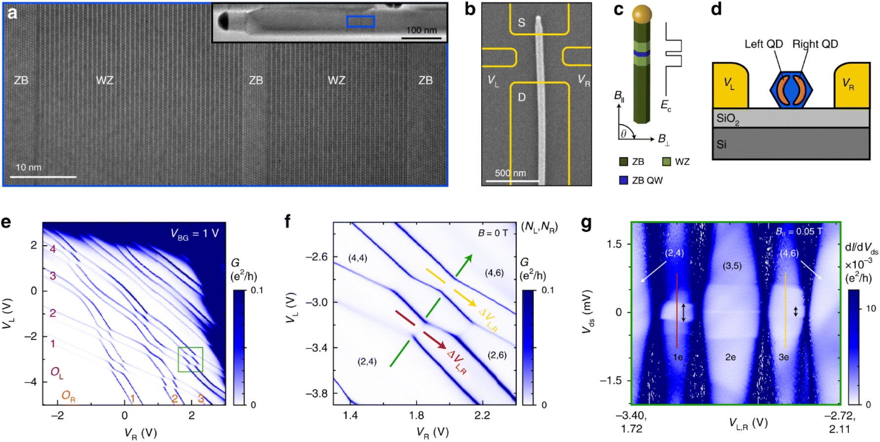 | ||
Fig. 7 (a) Transmission electron micrograph of a representative nanowire. The centre ZB segment acts as a quantum well accessed by WZ tunnel barriers. (b) SEM of the studied nanowire, overlaid with the contact design. (c) Schematic of the crystal structure and resulting conduction-band alignment. (d) Side-view illustration of the formation of two parallel-coupled QDs. (e) Conductance G as a function of side-gate voltages (VL, VR), where the orbital numbers (OL, OR) are indicated. (f) Magnification of the (OL, OR)![[thin space (1/6-em)]](https://www.rsc.org/images/entities/char_2009.gif) = (2, 3) crossing. Green, red, and yellow arrows indicate important gate vectors, and (NL, NR) represents the electron population on the left and right QD. (g) Measurement of dI/dVdsversus Vds along the green gate vector for B‖ = 0.05 T. The Zeeman splitting of the ground state 2EZ is indicated with arrows in the 1e and 3e regimes. From Fig. 1 by Potts, H., Chen, I., Tsintzis, A. et al., Electrical control of spins and giant g-factors in ring-like coupled quantum dots, Nat. Commun., 10, 5740, (2019), https://doi.org/10.1038/s41467-019-13583-7. Is licensed under CC BY 4.0. = (2, 3) crossing. Green, red, and yellow arrows indicate important gate vectors, and (NL, NR) represents the electron population on the left and right QD. (g) Measurement of dI/dVdsversus Vds along the green gate vector for B‖ = 0.05 T. The Zeeman splitting of the ground state 2EZ is indicated with arrows in the 1e and 3e regimes. From Fig. 1 by Potts, H., Chen, I., Tsintzis, A. et al., Electrical control of spins and giant g-factors in ring-like coupled quantum dots, Nat. Commun., 10, 5740, (2019), https://doi.org/10.1038/s41467-019-13583-7. Is licensed under CC BY 4.0. | ||
The electrostatics in the QW were manipulated using two side gates (VL and VR) and a back-gate (VBG). This way, two QDs, coupled to source and drain, form in the ZB-InAs segment (Fig. 7d). The DQD is proven by the honeycomb diagram observed in Fig. 7e. The strong confinement observed in the ZB-InAs is key in the electron population and occupancies of each QD and in the tunning of the inter-dot tunnel coupling thanks to the confinement provided by the crystal phase approach.171 The first orbital crossing (OL,R = 1) was probed in previous work of the same research group.171,177,178 However, in ref. 76 they focused on the conductance maps of the interactions of higher orbitals. A magnification of the crossing (OL, OR) = (2, 3) (highlighted in Fig. 7e), together with the electron population, is shown in Fig. 7f. In conductance maps, for a standard DQD configuration, sharp corners are interpreted as no inter-dot tunnelling, as it can be observed for the (2,3) crossing. In contrast, rounded corners appear when there is a clear hybridization gap as in the (2,2) crossing.
The differential conductance, dI/dVds, is represented in Fig. 7gversus the drain-source voltage (Vds) and the side-gate voltages (VL,R) for B‖ = 0.05 T aligned with the NWQD. Characteristic Coulomb diamonds are obtained in the dI/dV plot as a function of Vds and VL,R (Fig. 7g) for the 1, 2, and 3 electron regimes. The effective g*-factors obtained (∼64 and 40) were significantly larger than those for bulk InAs (−14.9).179,180
Moreover, they found interacting orbitals exhibiting an electronic structure almost identical to carbon nanotube (CNT) QDs (a quantum ring platform with a fourfold orbital- and spin-degeneracy, and anisotropic effective g*-factors), with highly anisotropic g*-factors varying from 3 to 80. However, in contrast to CNTs, it is possible to control the g*-factor from ∼80 to ∼0 using electric fields for the same charge state. Using perturbation theory, they confirmed that ring-like DQDs appear when one odd and one even orbital from each QD hybridize.
Quantum rings can also be employed to explore the Aharonov–Bohm (AB) effect as reported in 2022 by Debbarma and co-workers.181 The AB effect is a quantum mechanical phenomenon in which an electrically charged particle is affected by an electromagnetic potential, despite being confined to a region in which both the magnetic and electric fields are zero.182 In their work, they investigated two different kinds of crystal phase ZB-InAs (4–5 nm thick) ring-like QD structures (A and B). A pure ZB-InAs QD for sample A and the same structure together with a thin InAsSb shell for sample B. Surface band bending in the InAs and in the thin InAsSb shell is crucial for the appearance of the ring-like QD in InAs183 and InAsSb.184 The strong confinement inside the QD produced the absence of filled states, while electrons can accumulate close to the surface.76 However, the resulting ring-like states around the NW surface are sensitive to perturbations, resulting in localized electron states.171 They include two different samples to enhance the surface electron accumulation and to screen symmetry-breaking effects to further increase the spin–orbit interaction.
Fig. 8 shows the conductance and differential conductance maps for both type A and type B ring-like QDs. The conductance map as a function of VL,R of the type B sample does not show any honeycomb structure (Fig. 8a). This is an indication of transport through a single QD.185 They found that the level structure and magnetic field evolution (Fig. 8b) are similar to the observed for CNT QDs. From Fig. 8b, the authors extracted gorb = 290 and an upper limit for |gspin| of approximately 15, results that are consistent with those extracted from Fig. 8c. Moving to the type A structure, the conductance map (Fig. 8d) is explained by transport through a DQD parallel-coupled to source and drain.171,186 The numbering of the orbital crossings is indicated in the schematic in Fig. 8e. The authors highlight that the DQD is not ideal and the gate coupling to some orbitals is not constant over the whole measurement interval. They conclude that thanks to the strong phase coherence of the system, uncommon for non-superconducting rings, they could study theoretical predictions on the effects of symmetry and parity of a quantum ring. In this case, the crystal phase approach opens the possibility to engineer new material and crystal phase combinations that could provide an even more efficient manipulation of electronic states in ring-like DQDs.
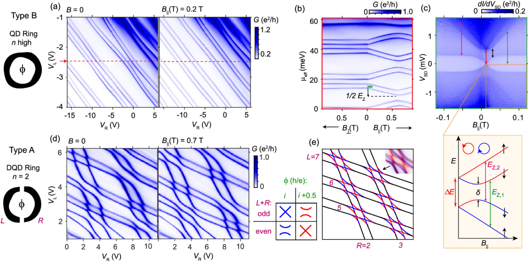 | ||
| Fig. 8 Effects of B-fields on orbital and spin states in QD rings with different symmetries (n). (a) Conductance of a QD ring (sample type B) as a function of VL,R at B = 0 (left) and B‖ = 0.2 T (right) for a back-gate voltage, VBG = 3 V, and source-drain voltage, VSD = 0.1 mV. (b) Conductance along the red line in panel a vs. B⊥ and B‖. (c) Differential conductance vs. B‖ in the one-electron regime along the green bar in panel B. The inset shows schematically how the four nearly degenerate spin and orbital states evolve with B‖, where it is possible to identify EZ and extract gorb from EZ = gorbμBB‖. (d) Conductance of a double QD ring (sample type A) for B = 0 and B‖ = 0.7 T at VBG = 0 V and VSD = 0.5 mV. (e) Schematic for six consecutive orbital crossings at ϕ = 0 and 0.5 h/e. Orbital parity and threaded flux (i, integer) determine whether each crossing is exact or avoided. The small inset shows an overlay of data from panel d at the two fields. From Fig. 2 by Debbarma. R, et al., Nano Lett., 2022, 22, 1, 334–339, https://doi.org/10.1021/acs.nanolett.1c03882 is licensed under CC BY 4.0. | ||
4. Conclusions
In this review article, we make a comprehensive revision of the field of crystal phase NWQDs. Traditionally NWQDs are formed via heterostructure interfaces between materials with different band gaps. However, their perfection is limited by the difficulty to control the interface abruptness and material composition at the atomic level, which unfortunately are determining factors for the physical properties of QDs as they define the shape of the potential well. Here, we discuss the growth of NWQDs in the axial direction varying the crystal phase, instead of the material composition, emphasizing the advantages offered by this approach. As this method employs a change in crystal structure instead of a change in material, then perfectly abrupt interfaces can be achieved. However, the band offset between WZ and ZB is fixed and relatively small, limiting the application of crystal phase QDs to liquid-He temperatures and to fields where the purity of the interface is more critical than the band offset. This is the case of the inspection of fundamental optical and quantum effects. We review the concepts of WZ and ZB crystal structures, supersaturation, and the different options available to control the crystal structure. For controlling the crystal phase, scientists have developed a method where only the group-V supply should be changed. In addition, different crystal phases offer different lateral facet terminations and, consequently, different surface energies, allowing to grow the shell in a selective fashion. That is, the shell can be grown either on the WZ or on the ZB phase of the core, thus leading to the formation of ring-like structures or enabling the growth of crystal phases that would be otherwise very difficult, if not impossible, to obtain. As an example, we describe the case of WZ-GaSb. Then, in Section 3, we discuss the optical and electronic properties of crystal phase NWQDs. The optical properties are focused on the type II transitions that appear in ZB-GaAs QDs and on the atomically sharp nature of the interface between WZ and ZB. Regarding the electronic properties, we mainly analyse the coupling between two QDs (forming DQDs) and the ring-like behaviour of ZB-InAs parallel-coupled DQDs. We strongly believe that crystal phase NWQDs are an excellent platform to discover new quantum phenomena either to probe theoretical models or to engineer new material architectures by means of the crystal structure transfer method.Conflicts of interest
There are no conflicts to declare.Acknowledgements
The authors acknowledge financial support from the Generalitat Valenciana (Projects: COMCUANTICA/003, CIAPOS/2021/293, and CDEIGENT/2020/009).Notes and references
- W. Zhou and J. J. Coleman, Semiconductor quantum dots, Curr. Opin. Solid State Mater. Sci., 2016, 20, 352–360 CrossRef CAS.
- M. T. Borgström, V. Zwiller, E. Müller and A. Imamoglu, Optically Bright Quantum Dots in Single Nanowires, Nano Lett., 2005, 5, 1439–1443 CrossRef PubMed.
- G. Bulgarini, M. E. Reimer, T. Zehender, M. Hocevar, E. P. A. M. Bakkers, L. P. Kouwenhoven and V. Zwiller, Spontaneous emission control of single quantum dots in bottom-up nanowire waveguides, Appl. Phys. Lett., 2012, 100, 121106 CrossRef.
- J. Claudon, J. Bleuse, N. S. Malik, M. Bazin, P. Jaffrennou, N. Gregersen, C. Sauvan, P. Lalanne and J. M. Gérard, A highly efficient single-photon source based on a quantum dot in a photonic nanowire, Nat. Photonics, 2010, 4, 174–177 CrossRef CAS.
- M. Munsch, N. S. Malik, E. Dupuy, A. Delga, J. Bleuse, J. M. Gérard, J. Claudon, N. Gregersen and J. M\ork, Dielectric GaAs Antenna Ensuring an Efficient Broadband Coupling between an InAs Quantum Dot and a Gaussian Optical Beam, Phys. Rev. Lett., 2013, 110, 177402 CrossRef PubMed.
- M. E. Reimer, G. Bulgarini, N. Akopian, M. Hocevar, M. B. Bavinck, M. A. Verheijen, E. P. A. M. Bakkers, L. P. Kouwenhoven and V. Zwiller, Bright single-photon sources in bottom-up tailored nanowires, Nat. Commun., 2012, 3, 737 CrossRef PubMed.
- I. Friedler, C. Sauvan, J. P. Hugonin, P. Lalanne, J. Claudon and J. M. Gérard, Solid-state single photon sources: the nanowire antenna, Opt. Express, 2009, 17, 2095–2110 CrossRef CAS PubMed.
- M. E. Reimer, M. P. van Kouwen, M. Barkelid, M. Hocevar, M. H. M. van Weert, R. E. Algra, E. P. A. M. Bakkers, M. T. Björk, H. Schmid, H. Riel, L. P. Kouwenhoven and V. Zwiller, Single photon emission and detection at the nanoscale utilizing semiconductor nanowires, J. Nanophotonics, 2011, 5, 53502 CrossRef.
- M. P. van Kouwen, M. H. M. van Weert, M. E. Reimer, N. Akopian, U. Perinetti, R. E. Algra, E. P. A. M. Bakkers, L. P. Kouwenhoven and V. Zwiller, Single quantum dot nanowire photodetectors, Appl. Phys. Lett., 2010, 97, 113108 CrossRef.
- D. Dalacu, K. Mnaymneh, J. Lapointe, X. Wu, P. J. Poole, G. Bulgarini, V. Zwiller and M. E. Reimer, Ultraclean Emission from InAsP Quantum Dots in Defect-Free Wurtzite InP Nanowires, Nano Lett., 2012, 12, 5919–5923 CrossRef CAS PubMed.
- J. Heinrich, A. Huggenberger, T. Heindel, S. Reitzenstein, S. Höfling, L. Worschech and A. Forchel, Single photon emission from positioned GaAs/AlGaAs photonic nanowires, Appl. Phys. Lett., 2010, 96, 211117 CrossRef.
- E. D. Minot, F. Kelkensberg, M. van Kouwen, J. A. van Dam, L. P. Kouwenhoven, V. Zwiller, M. T. Borgström, O. Wunnicke, M. A. Verheijen and E. P. A. M. Bakkers, Single Quantum Dot Nanowire LEDs, Nano Lett., 2007, 7, 367–371 CrossRef CAS PubMed.
- S. Nadj-Perge, S. M. Frolov, E. P. A. M. Bakkers and L. P. Kouwenhoven, Spin–orbit qubit in a semiconductor nanowire, Nature, 2010, 468, 1084–1087 CrossRef CAS PubMed.
- V. S. Pribiag, S. Nadj-Perge, S. M. Frolov, J. W. G. van den Berg, I. van Weperen, S. R. Plissard, E. P. A. M. Bakkers and L. P. Kouwenhoven, Electrical control of single hole spins in nanowire quantum dots, Nat. Nanotechnol., 2013, 8, 170–174 CrossRef CAS PubMed.
- N. Somaschi, V. Giesz, L. De Santis, J. C. Loredo, M. P. Almeida, G. Hornecker, S. L. Portalupi, T. Grange, C. Antón, J. Demory, C. Gómez, I. Sagnes, N. D. Lanzillotti-Kimura, A. Lemaítre, A. Auffeves, A. G. White, L. Lanco and P. Senellart, Near-optimal single-photon sources in the solid state, Nat. Photonics, 2016, 10, 340–345 CrossRef CAS.
- X. Ding, Y. He, Z. C. Duan, N. Gregersen, M. C. Chen, S. Unsleber, S. Maier, C. Schneider, M. Kamp, S. Höfling, C. Y. Lu and J. W. Pan, On-Demand Single Photons with High Extraction Efficiency and Near-Unity Indistinguishability from a Resonantly Driven Quantum Dot in a Micropillar, Phys. Rev. Lett., 2016, 116, 20401 CrossRef PubMed.
- S. Unsleber, Y. M. He, S. Gerhardt, S. Maier, C. Y. Lu, J. W. Pan, N. Gregersen, M. Kamp, C. Schneider and S. Höfling, Highly indistinguishable on-demand resonance fluorescence photons from a deterministic quantum dot micropillar device with 74%; extraction efficiency, Opt. Express, 2016, 24, 8539–8546 CrossRef CAS PubMed.
- L. Goldstein, F. Glas, J. Y. Marzin, M. N. Charasse and G. Le Roux, Growth by molecular beam epitaxy and characterization of InAs/GaAs strained-layer superlattices, Appl. Phys. Lett., 1985, 47, 1099–1101 CrossRef CAS.
- P. Lodahl, S. Mahmoodian and S. Stobbe, Interfacing single photons and single quantum dots with photonic nanostructures, Rev. Mod. Phys., 2015, 87, 347–400 CrossRef CAS.
- J. M. García, T. Mankad, P. O. Holtz, P. J. Wellman and P. M. Petroff, Electronic states tuning of InAs self-assembled quantum dots, Appl. Phys. Lett., 1998, 72, 3172–3174 CrossRef.
- C. P. Dietrich, A. Fiore, M. G. Thompson, M. Kamp and S. Höfling, GaAs integrated quantum photonics: Towards compact and multi-functional quantum photonic integrated circuits, Laser Photonics Rev., 2016, 10, 870–894 CrossRef CAS.
- V. J. Gómez, M. Marnauza, K. A. Dick and S. Lehmann, Growth selectivity control of InAs shells on crystal phase engineered GaAs nanowires, Nanoscale Adv., 2022, 4, 3330–3341 RSC.
- M. de la Mata, X. Zhou, F. Furtmayr, J. Teubert, S. Gradečak, M. Eickhoff, A. I. Morral and J. Arbiol, A review of MBE grown 0D, 1D and 2D quantum structures in a nanowire, J. Mater. Chem. C, 2013, 1, 4300–4312 RSC.
- L. Francaviglia, Y. Fontana and A. Fontcuberta i Morral, Semiconductors and Semimetals, Elsevier Inc., 2016, vol. 94, pp. 159–184 Search PubMed.
- K. A. Dick, P. Caroff, J. Bolinsson, M. E. Messing, J. Johansson, K. Deppert, L. R. Wallenberg and L. Samuelson, Control of III–V nanowire crystal structure by growth parameter tuning, Semicond. Sci. Technol., 2010, 25, 024009 CrossRef.
- P. Caroff, K. A. Dick, J. Johansson, M. E. Messing, K. Deppert and L. Samuelson, Controlled polytypic and twin-plane superlattices in III–V nanowires, Nat. Nanotechnol., 2009, 4, 50–55 CrossRef CAS PubMed.
- H. J. Joyce, J. Wong-Leung, Q. Gao, H. Hoe Tan and C. Jagadish, Phase perfection in zinc blende and wurtzite III–V nanowires using basic growth parameters, Nano Lett., 2010, 10, 908–915 CrossRef CAS PubMed.
- I. Geijselaers, N. Vainorius, S. Lehmann, C. E. Pryor, K. A. Dick and M. E. Pistol, Atomically sharp, crystal phase defined GaAs quantum dots, Appl. Phys. Lett., 2021, 119, 263102 CrossRef CAS.
- N. Vainorius, S. Lehmann, D. Jacobsson, L. Samuelson, K. A. Dick and M. E. Pistol, Confinement in Thickness-Controlled GaAs Polytype Nanodots, Nano Lett., 2015, 15, 2652–2656 CrossRef CAS PubMed.
- N. Akopian, G. Patriarche, L. Liu, J. C. Harmand and V. Zwiller, Crystal Phase Quantum Dots, Nano Lett., 2010, 10, 1198–1201 CrossRef CAS PubMed.
- N. Vainorius, D. Jacobsson, S. Lehmann, A. Gustafsson, K. A. Dick, L. Samuelson and M. E. Pistol, Observation of type-II recombination in single wurtzite/zinc-blende GaAs heterojunction nanowires, Phys. Rev. B, 2014, 89, 165423 CrossRef.
- M. Ek and M. A. Filler, Atomic-Scale Choreography of Vapor–Liquid–Solid Nanowire Growth, Acc. Chem. Res., 2018, 51, 118–126 CrossRef CAS PubMed.
- R. S. Wagner and W. C. Ellis, Vapor-liquid–solid mechanism of single crystal growth, Appl. Phys. Lett., 1964, 4, 89–90 CrossRef CAS.
- K. Hiruma, T. Katsuyama, K. Ogawa, M. Koguchi, H. Kakibayashi and G. P. Morgan, Quantum size microcrystals grown using organometallic vapor phase epitaxy, Appl. Phys. Lett., 1991, 59, 431–433 CrossRef CAS.
- M. Koguchi, H. Kakibayashi, M. Yazawa, K. H. K. Hiruma and T. K. T. Katsuyama, Crystal Structure Change of GaAs and InAs Whiskers from Zinc-Blende to Wurtzite Type, Jpn. J. Appl. Phys., 1992, 31, 2061 CrossRef CAS.
- M. Murayama and T. Nakayama, Chemical trend of band offsets at wurtzite/zinc-blende heterocrystalline semiconductor interfaces, Phys. Rev. B: Condens. Matter Mater. Phys., 1994, 49, 4710–4724 CrossRef CAS PubMed.
- R. E. Algra, M. A. Verheijen, M. T. Borgström, L. F. Feiner, G. Immink, W. J. P. van Enckevort, E. Vlieg and E. P. A. M. Bakkers, Twinning superlattices in indium phosphide nanowires, Nature, 2008, 456, 369–372 CrossRef CAS PubMed.
- P. Caroff, K. A. Dick, J. Johansson, M. E. Messing, K. Deppert and L. Samuelson, Controlled polytypic and twin-plane superlattices in III–V nanowires, Nat. Nanotechnol., 2009, 4, 50–55 CrossRef CAS.
- B. W. Jacobs, V. M. Ayres, R. E. Stallcup, A. Hartman, M. A. Tupta, A. D. Baczewski, M. A. Crimp, J. B. Halpern, M. He and H. C. Shaw, Electron transport in zinc-blende wurtzite biphasic gallium nitride nanowires and GaNFETs, Nanotechnology, 2007, 18, 475710 CrossRef.
- J. Bao, D. C. Bell, F. Capasso, J. B. Wagner, T. Mårtensson, J. Trägårdh and L. Samuelson, Optical Properties of Rotationally Twinned InP Nanowire Heterostructures, Nano Lett., 2008, 8, 836–841 CrossRef CAS PubMed.
- K. Pemasiri, M. Montazeri, R. Gass, L. M. Smith, H. E. Jackson, J. Yarrison-Rice, S. Paiman, Q. Gao, H. H. Tan, C. Jagadish, X. Zhang and J. Zou, Carrier Dynamics and Quantum Confinement in type II ZB–WZ InP Nanowire Homostructures, Nano Lett., 2009, 9, 648–654 CrossRef CAS PubMed.
- T. B. Hoang, A. F. Moses, H. L. Zhou, D. L. Dheeraj, B. O. Fimland and H. Weman, Observation of free exciton photoluminescence emission from single wurtzite GaAs nanowires, Appl. Phys. Lett., 2009, 94, 133105 CrossRef.
- H. J. Joyce, J. Wong-Leung, Q. Gao, H. H. Tan and C. Jagadish, Phase Perfection in Zinc Blende and Wurtzite III–V Nanowires Using Basic Growth Parameters, Nano Lett., 2010, 10, 908–915 CrossRef CAS PubMed.
- S. Lehmann, J. Wallentin, D. Jacobsson, K. Deppert and K. A. Dick, A general approach for sharp crystal phase switching in InAs, GaAs, InP, and GaP nanowires using only group v flow, Nano Lett., 2013, 13, 4099–4105 CrossRef CAS PubMed.
- J. Wallentin and M. T. Borgström, Doping of semiconductor nanowires, J. Mater. Res., 2011, 26, 2142–2156 CrossRef CAS.
- K. Tateno, G. Zhang, H. Gotoh and T. Sogawa, VLS Growth of Alternating InAsP/InP Heterostructure Nanowires for Multiple-Quantum-Dot Structures, Nano Lett., 2012, 12, 2888–2893 CrossRef CAS.
- L. Namazi, L. Gren, M. Nilsson, M. Garbrecht, C. Thelander, R. R. Zamani and K. A. Dick, Realization of Wurtzite GaSb Using InAs Nanowire Templates, Adv. Funct. Mater., 2018, 28, 1800512 CrossRef.
- K. A. Dick, A review of nanowire growth promoted by alloys and non-alloying elements with emphasis on Au-assisted III–V nanowires, Prog. Cryst. Growth Charact. Mater., 2008, 54, 138–173 CrossRef CAS.
- N. S. Tabrizi, M. Ullmann, V. A. Vons, U. Lafont and A. Schmidt-Ott, Generation of nanoparticles by spark discharge, J. Nanopart. Res., 2009, 11, 315–332 CrossRef CAS.
- M. H. Magnusson, K. Deppert, J. O. Malm, J. O. Bovin and L. Samuelson, Size-selected gold nanoparticles by aerosol technology, Nanostruct. Mater., 1999, 12, 45–48 CrossRef.
- H. Xu, Y. Wang, Y. Guo, Z. Liao, Q. Gao, N. Jiang, H. H. Tan, C. Jagadish and J. Zou, High-Density, Defect-Free, and Taper-Restrained Epitaxial GaAs Nanowires Induced from Annealed Au Thin Films, Cryst. Growth Des., 2012, 12, 2018–2022 CrossRef CAS.
- V. J. Gómez, M. Graczyk, R. J. Jam, S. Lehmann and I. Maximov, Wafer-scale nanofabrication of sub-100 nm arrays by deep-UV displacement Talbot lithography, Nanotechnology, 2020, 31, 295301 CrossRef PubMed.
- S. L. Diedenhofen, O. T. A. Janssen, M. Hocevar, A. Pierret, E. P. A. M. Bakkers, H. P. Urbach and J. Gómez Rivas, Controlling the Directional Emission of Light by Periodic Arrays of Heterostructured Semiconductor Nanowires, ACS Nano, 2011, 5, 5830–5837 CrossRef CAS PubMed.
- Y. Fontana, G. Grzela, E. P. A. M. Bakkers and J. G. Rivas, Mapping the directional emission of quasi-two-dimensional photonic crystals of semiconductor nanowires using Fourier microscopy, Phys. Rev. B: Condens. Matter Mater. Phys., 2012, 86, 245303 CrossRef.
- S. Assali, L. Gagliano, D. S. Oliveira, M. A. Verheijen, S. R. Plissard, L. F. Feiner and E. P. A. M. Bakkers, Exploring Crystal Phase Switching in GaP Nanowires, Nano Lett., 2015, 15, 8062–8069 CrossRef CAS PubMed.
- J. Vukajlovic-Plestina, W. Kim, L. Ghisalberti, G. Varnavides, G. Tütüncuoglu, H. Potts, M. Friedl, L. Güniat, W. C. Carter, V. G. Dubrovskii and A. Fontcuberta i Morral, Fundamental aspects to localize self-catalyzed III–V nanowires on silicon, Nat. Commun., 2019, 10, 869 CrossRef CAS PubMed.
- F. Panciera, Z. Baraissov, G. Patriarche, V. G. Dubrovskii, F. Glas, L. Travers, U. Mirsaidov and J. C. Harmand, Phase Selection in Self-catalyzed GaAs Nanowires, Nano Lett., 2020, 20, 1669–1675 CrossRef CAS PubMed.
- B. Mandl, J. Stangl, E. Hilner, A. A. Zakharov, K. Hillerich, A. W. Dey, L. Samuelson, G. Bauer, K. Deppert and A. Mikkelsen, Growth Mechanism of Self-Catalyzed Group III–V Nanowires, Nano Lett., 2010, 10, 4443–4449 CrossRef CAS.
- K. Ikejiri, J. Noborisaka, S. Hara, J. Motohisa and T. Fukui, Mechanism of catalyst-free growth of GaAs nanowires by selective area MOVPE, J. Cryst. Growth, 2007, 298, 616–619 CrossRef CAS.
- Q. Gao, D. Saxena, F. Wang, L. Fu, S. Mokkapati, Y. Guo, L. Li, J. Wong-Leung, P. Caroff, H. H. Tan and C. Jagadish, Selective-Area Epitaxy of Pure Wurtzite InP Nanowires: High Quantum Efficiency and Room-Temperature Lasing, Nano Lett., 2014, 14, 5206–5211 CrossRef CAS.
- Y. Kitauchi, Y. Kobayashi, K. Tomioka, S. Hara, K. Hiruma, T. Fukui and J. Motohisa, Structural Transition in Indium Phosphide Nanowires, Nano Lett., 2010, 10, 1699–1703 CrossRef CAS PubMed.
- K. Tomioka, K. Ikejiri, T. Tanaka, J. Motohisa, S. Hara, K. Hiruma and T. Fukui, Selective-area growth of III–V nanowires and their applications, J. Mater. Res., 2011, 26, 2127–2141 CrossRef CAS.
- J. Tatebayashi, Y. Ota, S. Ishida, M. Nishioka, S. Iwamoto and Y. Arakawa, Highly uniform, multi-stacked InGaAs/GaAs quantum dots embedded in a GaAs nanowire, Appl. Phys. Lett., 2014, 105, 103104 CrossRef.
- K. P. Bassett, P. K. Mohseni and X. Li, Evolution of GaAs nanowire geometry in selective area epitaxy, Appl. Phys. Lett., 2015, 106, 133102 CrossRef.
- Y. Kohashi, S. Sakita, S. Hara and J. Motohisa, Pitch-Independent Realization of 30-nm-Diameter InGaAs Nanowire Arrays by Two-Step Growth Method in Selective-Area Metalorganic Vapor-Phase Epitaxy, Appl. Phys. Express, 2013, 6, 25502 CrossRef.
- Y. Kohashi, T. Sato, K. Ikejiri, K. Tomioka, S. Hara and J. Motohisa, Influence of growth temperature on growth of InGaAs nanowires in selective-area metal–organic vapor-phase epitaxy, J. Cryst. Growth, 2012, 338, 47–51 CrossRef CAS.
- K. A. Dick and P. Caroff, Metal-seeded growth of III–V semiconductor nanowires: Towards gold-free synthesis, Nanoscale, 2014, 6, 3006–3021 RSC.
- B. J. Ohlsson, M. T. Björk, A. I. Persson, C. Thelander, L. R. Wallenberg, M. H. Magnusson, K. Deppert and L. Samuelson, Growth and characterization of GaAs and InAs nano-whiskers and InAs/GaAs heterostructures, Phys. E, 2002, 13, 1126–1130 CrossRef CAS.
- A. i Morral, C. Colombo, G. Abstreiter, J. Arbiol and J. R. Morante, Nucleation mechanism of gallium-assisted molecular beam epitaxy growth of gallium arsenide nanowires, Appl. Phys. Lett., 2008, 92, 63112 CrossRef.
- C. B. Maliakkal, M. Tornberg, D. Jacobsson, S. Lehmann and K. A. Dick, Vapor–solid–solid growth dynamics in GaAs nanowires, Nanoscale Adv., 2021, 3, 5928–5940 RSC.
- D. Jacobsson, F. Panciera, J. Tersoff, M. C. Reuter, S. Lehmann, S. Hofmann, K. A. Dick and F. M. Ross, Interface dynamics and crystal phase switching in GaAs nanowires, Nature, 2016, 531, 317–322 CrossRef CAS PubMed.
- Z. Su, N. Wang, H. H. Tan and C. Jagadish, 2D Carrier Localization at the Wurtzite–Zincblende Interface in Novel Layered InP Nanomembranes, ACS Photonics, 2021, 8, 1735–1745 CrossRef CAS.
- N. Wang, W. W. Wong, X. Yuan, L. Li, C. Jagadish and H. H. Tan, Understanding Shape Evolution and Phase Transition in InP Nanostructures Grown by Selective Area Epitaxy, Small, 2021, 17, 2100263 CrossRef CAS PubMed.
- P. Staudinger, S. Mauthe, N. V. Triviño, S. Reidt, K. E. Moselund and H. Schmid, Wurtzite InP microdisks: from epitaxy to room-temperature lasing, Nanotechnology, 2020, 32, 75605 CrossRef PubMed.
- H. Mäntynen, N. Anttu, Z. Sun and H. Lipsanen, Single-photon sources with quantum dots in III–V nanowires, Nanophotonics, 2019, 8, 747–769 Search PubMed.
- H. Potts, I. J. Chen, A. Tsintzis, M. Nilsson, S. Lehmann, K. A. Dick, M. Leijnse and C. Thelander, Electrical control of spins and giant g-factors in ring-like coupled quantum dots, Nat. Commun., 2019, 10, 5740 CrossRef CAS PubMed.
- T. Y. Chang, H. Kim, W. A. Hubbard, K. M. Azizur-Rahman, J. J. Ju, J. H. Kim, W. J. Lee and D. Huffaker, InAsP Quantum Dot-Embedded InP Nanowires toward Silicon Photonic Applications, ACS Appl. Mater. Interfaces, 2022, 14, 12488–12494 CrossRef CAS PubMed.
- T. Y. Chang, H. Kim, B. T. Zutter, W. J. Lee, B. C. Regan and D. L. Huffaker, Orientation-Controlled Selective-Area Epitaxy of III–V Nanowires on (001) Silicon for Silicon Photonics, Adv. Funct. Mater., 2020, 30, 2002220 CrossRef CAS.
- M. Jeannin, T. Cremel, T. Häyrynen, N. Gregersen, E. Bellet-Amalric, G. Nogues and K. Kheng, Enhanced Photon Extraction from a Nanowire Quantum Dot Using a Bottom-Up Photonic Shell, Phys. Rev. Appl., 2017, 8, 54022 CrossRef.
- G. Priante, F. Glas, G. Patriarche, K. Pantzas, F. Oehler and J. C. Harmand, Sharpening the Interfaces of Axial Heterostructures in Self-Catalyzed AlGaAs Nanowires: Experiment and Theory, Nano Lett., 2016, 16, 1917–1924 CrossRef CAS PubMed.
- R. S. Bauer and H. W. Sang, On the adjustability of the “abrupt” heterojunction band-gap discontinuity, Surf. Sci., 1983, 132, 479–504 CrossRef CAS.
- E. Luna, Á. Guzmán, A. Trampert and G. Álvarez, Critical role of two-dimensional island-mediated growth on the formation of semiconductor heterointerfaces, Phys. Rev. Lett., 2012, 109, 1–5 CrossRef PubMed.
- M. Nilsson, L. Namazi, S. Lehmann, M. Leijnse, K. A. Dick and C. Thelander, Single-electron transport in InAs nanowire quantum dots formed by crystal phase engineering, Phys. Rev. B, 2016, 93, 1–7 Search PubMed.
- J. V. Knutsson, S. Lehmann, M. Hjort, E. Lundgren, K. A. Dick, R. Timm and A. Mikkelsen, Electronic Structure Changes Due to Crystal Phase Switching at the Atomic Scale Limit, ACS Nano, 2017, 11, 10519–10528 CrossRef CAS PubMed.
- S. Lehmann, D. Jacobsson, K. Deppert and K. A. Dick, High crystal quality wurtzite-zinc blende heterostructures in metal-organic vapor phase epitaxy-grown GaAs nanowires, Nano Res., 2012, 5, 470–476 CrossRef CAS.
- C. Y. Yeh, Z. W. Lu, S. Froyen and A. Zunger, Zinc-blende–wurtzite polytypism in semiconductors, Phys. Rev. B: Condens. Matter Mater. Phys., 1992, 46, 10086–10097 CrossRef CAS PubMed.
- M. Bouwes Bavinck, K. D. Jöns, M. Zieliński, G. Patriarche, J. C. Harmand, N. Akopian and V. Zwiller, Photon Cascade from a Single Crystal Phase Nanowire Quantum Dot, Nano Lett., 2016, 16, 1081–1085 CrossRef CAS PubMed.
- A. Belabbes, C. Panse, J. Furthmüller and F. Bechstedt, Electronic bands of III–V semiconductor polytypes and their alignment, Phys. Rev. B: Condens. Matter Mater. Phys., 2012, 86, 75208 CrossRef.
- K. A. Dick, P. Caroff, J. Bolinsson, M. E. Messing, J. Johansson, K. Deppert, L. R. Wallenberg and L. Samuelson, Control of III–V nanowire crystal structure by growth parameter tuning, Semicond. Sci. Technol., 2010, 25, 24009 CrossRef.
- R. L. Woo, R. Xiao, Y. Kobayashi, L. Gao, N. Goel, M. K. Hudait, T. E. Mallouk and R. F. Hicks, Effect of Twinning on the Photoluminescence and Photoelectrochemical Properties of Indium Phosphide Nanowires Grown on Silicon (111), Nano Lett., 2008, 8, 4664–4669 CrossRef CAS PubMed.
- B. Liu, Y. Bando, C. Tang, F. Xu, J. Hu and D. Golberg, Needlelike Bicrystalline GaN Nanowires with Excellent Field Emission Properties, J. Phys. Chem. B, 2005, 109, 17082–17085 CrossRef CAS PubMed.
- Z. Chen, C. B. Cao and H. S. Zhu, Oriented Bicrystalline GaN Nanowire Arrays suitable for Field Emission Applications, Chem. Vap. Deposition, 2007, 13, 527–532 CrossRef CAS.
- Y. Chen, T. Burgess, X. An, Y. W. Mai, H. H. Tan, J. Zou, S. P. Ringer, C. Jagadish and X. Liao, Effect of a High Density of Stacking Faults on the Young's Modulus of GaAs Nanowires, Nano Lett., 2016, 16, 1911–1916 CrossRef CAS PubMed.
- H. Shtrikman, R. Popovitz-Biro, A. Kretinin, L. Houben, M. Heiblum, M. Bukała, M. Galicka, R. Buczko and P. Kacman, Method for Suppression of Stacking Faults in Wurtzite III–V Nanowires, Nano Lett., 2009, 9, 1506–1510 CrossRef CAS PubMed.
- P. K. Mohseni and R. R. LaPierre, A growth interruption technique for stacking fault-free nanowire superlattices, Nanotechnology, 2008, 20, 25610 CrossRef PubMed.
- F. Bechstedt and A. Belabbes, Structure, energetics, and electronic states of III–V compound polytypes, J. Phys.: Condens. Matter, 2013, 25, 273201 CrossRef PubMed.
- J. Johansson, Z. Zanolli and K. A. Dick, Polytype Attainability in III–V Semiconductor Nanowires, Cryst. Growth Des., 2016, 16, 371–379 CrossRef CAS.
- N. V. Sibirev, M. A. Timofeeva, A. D. Bol’shakov, M. V. Nazarenko and V. G. Dubrovskii, Surface energy and crystal structure of nanowhiskers of III–V semiconductor compounds, Phys. Solid State, 2010, 52, 1531–1538 CrossRef CAS.
- V. Pankoke, P. Kratzer and S. Sakong, Calculation of the diameter-dependent polytypism in GaAs nanowires from an atomic motif expansion of the formation energy, Phys. Rev. B: Condens. Matter Mater. Phys., 2011, 84, 75455 CrossRef.
- R. Leitsmann and F. Bechstedt, Surface influence on stability and structure of hexagon-shaped III–V semiconductor nanorods, J. Appl. Phys., 2007, 102, 63528 CrossRef.
- M. Rosini and R. Magri, Surface Effects on the Atomic and Electronic Structure of Unpassivated GaAs Nanowires, ACS Nano, 2010, 4, 6021–6031 CrossRef CAS PubMed.
- D. M. Cornet, V. G. M. Mazzetti and R. R. LaPierre, Onset of stacking faults in InP nanowires grown by gas source molecular beam epitaxy, Appl. Phys. Lett., 2007, 90, 13116 CrossRef.
- R. Sjökvist, M. Tornberg, M. Marnauza, D. Jacobsson and K. A. Dick, Observation of the Multilayer Growth Mode in Ternary InGaAs Nanowires, ACS Nanosci. Au, 2022, 2(6), 539–548 CrossRef.
- L. Namazi, M. Nilsson, S. Lehmann, C. Thelander and K. A. Dick, Selective GaSb radial growth on crystal phase engineered InAs nanowires, Nanoscale, 2015, 7, 10472–10481 RSC.
- M. Paladugu, J. Zou, Y. N. N. Guo, X. Zhang, Y. Kim, H. J. Joyce, Q. Gao, H. H. Tan and C. Jagadish, Polarity driven formation of InAs/GaAs hierarchical nanowire heterostructures, Appl. Phys. Lett., 2008, 93, 101911 CrossRef.
- S. Vlassov, S. Oras, B. Polyakov, E. Butanovs, A. Kyritsakis and V. Zadin, Kinking in Semiconductor Nanowires: A Review, Cryst. Growth Des., 2022, 22, 871–892 CrossRef CAS.
- J. C. Harmand, G. Patriarche, F. Glas, F. Panciera, I. Florea, J. L. Maurice, L. Travers and Y. Ollivier, Atomic Step Flow on a Nanofacet, Phys. Rev. Lett., 2018, 121, 166101 CrossRef CAS PubMed.
- A. D. Gamalski, J. Tersoff and E. A. Stach, Atomic Resolution in situ Imaging of a Double-Bilayer Multistep Growth Mode in Gallium Nitride Nanowires, Nano Lett., 2016, 16, 2283–2288 CrossRef CAS PubMed.
- S. Hofmann, R. Sharma, C. T. Wirth, F. Cervantes-Sodi, C. Ducati, T. Kasama, R. E. Dunin-Borkowski, J. Drucker, P. Bennett and J. Robertson, Ledge-flow-controlled catalyst interface dynamics during Si nanowire growth, Nat. Mater., 2008, 7, 372–375 CrossRef CAS PubMed.
- F. Glas, J. C. Harmand and G. Patriarche, Why Does Wurtzite Form in Nanowires of III–V Zinc Blende Semiconductors?, Phys. Rev. Lett., 2007, 99, 146101 CrossRef PubMed.
- J. Johansson, L. S. Karlsson, C. P. T. Svensson, T. Mårtensson, B. A. Wacaser, K. Deppert, L. Samuelson and W. Seifert, Structural properties of 〈111〉B -oriented III–V nanowires, Nat. Mater., 2006, 5, 574–580 CrossRef CAS PubMed.
- V. G. Dubrovskii, Refinement of Nucleation Theory for Vapor–Liquid–Solid Nanowires, Cryst. Growth Des., 2017, 17, 2589–2593 CrossRef CAS.
- F. Glas, J. C. Harmand and G. Patriarche, Nucleation Antibunching in Catalyst-Assisted Nanowire Growth, Phys. Rev. Lett., 2010, 104, 135501 CrossRef PubMed.
- C. B. Maliakkal, E. K. Mårtensson, M. U. Tornberg, D. Jacobsson, A. R. Persson, J. Johansson, L. R. Wallenberg and K. A. Dick, Independent Control of Nucleation and Layer Growth in Nanowires, ACS Nano, 2020, 14, 3868–3875 CrossRef CAS PubMed.
- M. Tornberg, R. Sjökvist, K. Kumar, C. R. Andersen, C. B. Maliakkal, D. Jacobsson and K. A. Dick, Direct Observations of Twin Formation Dynamics in Binary Semiconductors, ACS Nanosci. Au, 2022, 2, 49–56 CrossRef CAS.
- E. K. Mårtensson, J. Johansson and K. A. Dick, Simulating Vapor–Liquid–Solid Growth of Au-Seeded InGaAs Nanowires, ACS Nanosci. Au, 2022, 2, 239–249 CrossRef.
- K. A. Dick, J. Bolinsson, M. E. Messing, S. Lehmann, J. Johansson and P. Caroff, Parameter space mapping of InAs nanowire crystal structure, J. Vac. Sci. Technol., B, 2011, 29, 04D103 CrossRef.
- G. B. Stringfellow, Organometallic Vapor-Phase Epitaxy, ed. G. B. Stringfellow, Academic Press, 2nd edn, 1999, DOI:10.1016/B978-012673842-1/50004-1.
- J. Johansson, K. A. Dick, P. Caroff, M. E. Messing, J. Bolinsson, K. Deppert and L. Samuelson, Diameter Dependence of the Wurtzite−Zinc Blende Transition in InAs Nanowires, J. Phys. Chem. C, 2010, 114, 3837–3842 CrossRef CAS.
- S. A. Dayeh and S. T. Picraux, Direct Observation of Nanoscale Size Effects in Ge Semiconductor Nanowire Growth, Nano Lett., 2010, 10, 4032–4039 CrossRef CAS PubMed.
- V. G. Dubrovskii, Influence of the group V element on the chemical potential and crystal structure of Au-catalyzed III-V nanowires, Appl. Phys. Lett., 2014, 104, 053110 CrossRef.
- V. G. Dubrovskii, N. V Sibirev, J. C. Harmand and F. Glas, Growth Kinetics and Crystal Structure of Semiconductor Nanowires, Phys. Rev. B: Condens. Matter Mater. Phys., 2008, 78, 235301 CrossRef.
- T. Akiyama, K. Sano, K. Nakamura and T. Ito, An empirical potential approach to wurtzite-zinc-blende polytypism in group III–V semiconductor nanowires, Jpn. J. Appl. Phys., 2006, 45, L275 CrossRef CAS.
- V. G. Dubrovskii and N. V Sibirev, Growth thermodynamics of nanowires and its application to polytypism of zinc blende III–V nanowires, Phys. Rev. B: Condens. Matter Mater. Phys., 2008, 77, 35414 CrossRef.
- M. Galicka, M. Bukała, R. Buczko and P. Kacman, Modelling the structure of GaAs and InAs nanowires, J. Phys.: Condens. Matter, 2008, 20, 454226 CrossRef.
- E. Gil, V. G. Dubrovskii, G. Avit, Y. André, C. Leroux, K. Lekhal, J. Grecenkov, A. Trassoudaine, D. Castelluci, G. Monier, R. M. Ramdani, C. Robert-Goumet, L. Bideux, J. C. Harmand and F. Glas, Record Pure Zincblende Phase in GaAs Nanowires down to 5 nm in Radius, Nano Lett., 2014, 14, 3938 CrossRef CAS PubMed.
- E. K. Mårtensson, S. Lehmann, K. A. Dick and J. Johansson, Simulation of GaAs Nanowire Growth and Crystal Structure, Nano Lett., 2019, 19, 1197–1203 CrossRef PubMed.
- E. K. Mårtensson, S. Lehmann, K. A. Dick and J. Johansson, Effect of Radius on Crystal Structure Selection in III–V Nanowire Growth, Cryst. Growth Des., 2020, 20, 5373–5379 CrossRef.
- C. Thelander, P. Caroff, S. Plissard, A. W. Dey and K. A. Dick, Effects of crystal phase mixing on the electrical properties of InAs nanowires, Nano Lett., 2011, 11, 2424–2429 CrossRef CAS PubMed.
- R. E. Algra, M. A. Verheijen, L. F. Feiner, G. G. W. Immink, W. J. P. van Enckevort, E. Vlieg and E. P. A. M. Bakkers, The Role of Surface Energies and Chemical Potential during Nanowire Growth, Nano Lett., 2011, 11, 1259–1264 CrossRef CAS PubMed.
- J. Wallentin, K. Mergenthaler, M. Ek, L. R. Wallenberg, L. Samuelson, K. Deppert, M. E. Pistol and M. T. Borgström, Probing the Wurtzite Conduction Band Structure Using State Filling in Highly Doped InP Nanowires, Nano Lett., 2011, 11, 2286–2290 CrossRef CAS PubMed.
- D. Jacobsson, S. Lehmann and K. A. Dick, Crystal structure tuning in GaAs nanowires using HCl, Nanoscale, 2014, 6, 8257–8264 RSC.
- T. Xu, K. A. Dick, S. Plissard, T. H. Nguyen, Y. Makoudi, M. Berthe, J. P. Nys, X. Wallart, B. Grandidier and P. Caroff, Faceting, composition and crystal phase evolution in III–V antimonide nanowire heterostructures revealed by combining microscopy techniques, Nanotechnology, 2012, 23, 95702 CrossRef PubMed.
- D. Anandan, V. Nagarajan, R. K. Kakkerla, H. W. Yu, H. L. Ko, S. K. Singh, C. T. Lee and E. Y. Chang, Crystal phase control in self-catalyzed InSb nanowires using basic growth parameter V/III ratio, J. Cryst. Growth, 2019, 522, 30–36 CrossRef CAS.
- S. Lehmann, D. Jacobsson and K. A. Dick, Crystal phase control in GaAs nanowires: Opposing trends in the Ga- and As-limited growth regimes, Nanotechnology, 2015, 26, 301001 CrossRef PubMed.
- M. C. Plante and R. R. LaPierre, Control of GaAs nanowire morphology and crystal structure, Nanotechnology, 2008, 19, 495603 CrossRef CAS PubMed.
- G. E. Cirlin, V. G. Dubrovskii, Y. B. Samsonenko, A. D. Bouravleuv, K. Durose, Y. Y. Proskuryakov, B. Mendes, L. Bowen, M. A. Kaliteevski, R. A. Abram and D. Zeze, Self-catalyzed, pure zincblende GaAs nanowires grown on Si(111) by molecular beam epitaxy, Phys. Rev. B, 2010, 82, 35302 CrossRef.
- M. Soda, A. Rudolph, D. Schuh, J. Zweck, D. Bougeard and E. Reiger, Transition from Au to pseudo-Ga catalyzed growth mode observed in GaAs nanowires grown by molecular beam epitaxy, Phys. Rev. B, 2012, 85, 245450 CrossRef.
- P. Krogstrup, M. Hannibal Madsen, W. Hu, M. Kozu, Y. Nakata, J. Nygård, M. Takahasi and R. Feidenhans’l, In-situ x-ray characterization of wurtzite formation in GaAs nanowires, Appl. Phys. Lett., 2012, 100, 93103 CrossRef.
- T. Rieger, M. I. Lepsa, T. Schäpers and D. Grützmacher, Controlled wurtzite inclusions in self-catalyzed zinc blende III–V semiconductor nanowires, J. Cryst. Growth, 2013, 378, 506–510 CrossRef CAS.
- P. Krogstrup, R. Popovitz-Biro, E. Johnson, M. H. Madsen, J. Nygård and H. Shtrikman, Structural Phase Control in Self-Catalyzed Growth of GaAs Nanowires on Silicon (111), Nano Lett., 2010, 10, 4475–4482 CrossRef CAS PubMed.
- S. Paiman, Q. Gao, H. J. Joyce, Y. Kim, H. H. Tan, C. Jagadish, X. Zhang, Y. Guo and J. Zou, Growth temperature and V/III ratio effects on the morphology and crystal structure of InP nanowires, J. Phys. D: Appl. Phys., 2010, 43, 445402 CrossRef.
- S. Assali, I. Zardo, S. Plissard, D. Kriegner, M. A. Verheijen, G. Bauer, A. Meijerink, A. Belabbes, F. Bechstedt, J. E. M. Haverkort and E. P. A. M. Bakkers, Direct Band Gap Wurtzite Gallium Phosphide Nanowires, Nano Lett., 2013, 13, 1559–1563 CrossRef CAS PubMed.
- A. Berg, S. Lehmann, N. Vainorius, A. Gustafsson, M. E. Pistol, L. R. Wallenberg, L. Samuelson and M. T. Borgström, Growth and characterization of wurtzite GaP nanowires with control over axial and radial growth by use of HCl in-situ etching, J. Cryst. Growth, 2014, 386, 47–51 CrossRef CAS.
- E. Husanu, D. Ercolani, M. Gemmi and L. Sorba, Growth of defect-free GaP nanowires, Nanotechnology, 2014, 25, 205601 CrossRef PubMed.
- D. Spirkoska, J. Arbiol, A. Gustafsson, S. Conesa-Boj, F. Glas, I. Zardo, M. Heigoldt, M. H. Gass, A. L. Bleloch, S. Estrade, M. Kaniber, J. Rossler, F. Peiro, J. R. Morante, G. Abstreiter, L. Samuelson and A. I. Morral, Structural and optical properties of high quality zinc-blende/wurtzite GaAs nanowire heterostructures, Phys. Rev. B: Condens. Matter Mater. Phys., 2009, 80, 245325 CrossRef.
- M. Yamaguchi, J. H. Paek and H. Amano, Probability of twin formation on self-catalyzed GaAs nanowires on Si substrate, Nanoscale Res. Lett., 2012, 7, 558 CrossRef PubMed.
- V. J. Gómez, M. Marnauza, K. A. Dick and S. Lehmann, Growth selectivity control of InAs shells on crystal phase engineered GaAs nanowires, Nanoscale Adv., 2022, 4(16), 3330–3341 RSC.
- T. Rieger, T. Scha, D. Gru and M. I. Lepsa, Crystal Phase Selective Growth in GaAs/InAs Core − Shell Nanowires, Cryst. Growth Des., 2014, 14, 1167–1174 CrossRef CAS.
- L. Namazi, L. Gren, M. Nilsson, M. Garbrecht, C. Thelander, R. R. Zamani and K. A. Dick, Realization of Wurtzite GaSb Using InAs Nanowire Templates, Adv. Funct. Mater., 2018, 28, 1–13 Search PubMed.
- H. Kindlund, R. R. Zamani, A. R. Persson, S. Lehmann, L. R. Wallenberg and K. A. Dick, Kinetic Engineering of Wurtzite and Zinc-Blende AlSb Shells on InAs Nanowires, Nano Lett., 2018, 18, 5775–5781 CrossRef CAS PubMed.
- H. I. T. Hauge, M. A. Verheijen, S. Conesa-Boj, T. Etzelstorfer, M. Watzinger, D. Kriegner, I. Zardo, C. Fasolato, F. Capitani, P. Postorino, S. Kölling, A. Li, S. Assali, J. Stangl and E. P. A. M. Bakkers, Hexagonal Silicon Realized, Nano Lett., 2015, 15, 5855–5860 CrossRef CAS PubMed.
- P. Caroff, J. Bolinsson and J. Johansson, Crystal phases in III–V nanowires: From random toward engineered polytypism, IEEE J. Sel. Top. Quantum Electron., 2011, 17, 829–846 CAS.
- B. Ketterer, M. Heiss, E. Uccelli, J. Arbiol and A. Fontcuberta i Morral, Untangling the Electronic Band Structure of Wurtzite GaAs Nanowires by Resonant Raman Spectroscopy, ACS Nano, 2011, 5, 7585–7592 CrossRef CAS PubMed.
- M. Heiss, S. Conesa-Boj, J. Ren, H. H. Tseng, A. Gali, A. Rudolph, E. Uccelli, F. Peiró, J. R. Morante, D. Schuh, E. Reiger, E. Kaxiras, J. Arbiol and A. i Morral, Direct correlation of crystal structure and optical properties in wurtzite/zinc-blende GaAs nanowire heterostructures, Phys. Rev. B: Condens. Matter Mater. Phys., 2011, 83, 45303 CrossRef.
- A. De and C. E. Pryor, Predicted band structures of III–V semiconductors in the wurtzite phase, Phys. Rev. B: Condens. Matter Mater. Phys., 2010, 81, 155210 CrossRef.
- A. Mishra, L. V Titova, T. B. Hoang, H. E. Jackson, L. M. Smith, J. M. Yarrison-Rice, Y. Kim, H. J. Joyce, Q. Gao, H. H. Tan and C. Jagadish, Polarization and temperature dependence of photoluminescence from zincblende and wurtzite InP nanowires, Appl. Phys. Lett., 2007, 91, 263104 CrossRef.
- E. G. Gadret, G. O. Dias, L. C. O. Dacal, M. M. de Lima, C. V. R. S. Ruffo, F. Iikawa, M. J. S. P. Brasil, T. Chiaramonte, M. A. Cotta, L. H. G. Tizei, D. Ugarte and A. Cantarero, Valence-band splitting energies in wurtzite InP nanowires: Photoluminescence spectroscopy and ab initio calculations, Phys. Rev. B: Condens. Matter Mater. Phys., 2010, 82, 125327 CrossRef.
- T. T. T. Vu, T. Zehender, M. A. Verheijen, S. R. Plissard, G. W. G. Immink, J. E. M. Haverkort and E. P. A. M. Bakkers, High optical quality single crystal phase wurtzite and zincblende InP nanowires, Nanotechnology, 2013, 24, 115705 CrossRef PubMed.
- I. Geijselaers, S. Lehmann, K. A. Dick and M. E. Pistol, Two-dimensional electron gas at wurtzite–zinc-blende InP interfaces induced by modulation doping, Appl. Phys. Lett., 2020, 116, 232103 CrossRef CAS.
- L. H. Galvão Tizei and M. Amato, Electronic structure and optical properties of semiconductor nanowires polytypes, Eur. Phys. J. B, 2020, 93, 16 CrossRef.
- N. Vainorius, S. Lehmann, A. Gustafsson, L. Samuelson, K. A. Dick and M. E. Pistol, Wurtzite GaAs Quantum Wires: One-Dimensional Subband Formation, Nano Lett., 2016, 16, 2774–2780 CrossRef CAS PubMed.
- Z. B. Tan, D. Cox, T. Nieminen, P. Lähteenmäki, D. Golubev, G. B. Lesovik and P. J. Hakonen, Cooper pair splitting by means of graphene quantum dots, Phys. Rev. Lett., 2015, 114, 1–5 Search PubMed.
- L. G. Herrmann, F. Portier, P. Roche, A. L. Yeyati, T. Kontos and C. Strunk, Carbon nanotubes as cooper-pair beam splitters, Phys. Rev. Lett., 2010, 104, 1–4 CrossRef PubMed.
- M. C. Hels, B. Braunecker, K. Grove-Rasmussen and J. Nyg\aard, Noncollinear Spin-Orbit Magnetic Fields in a Carbon Nanotube Double Quantum Dot, Phys. Rev. Lett., 2016, 117, 276802 CrossRef CAS PubMed.
- J. C. Estrada Saldaña, A. Vekris, G. Steffensen, R. Žitko, P. Krogstrup, J. Paaske, K. Grove-Rasmussen and J. Nygård, Supercurrent in a Double Quantum Dot, Phys. Rev. Lett., 2018, 121, 257701 CrossRef PubMed.
- K. Grove-Rasmussen, G. Steffensen, A. Jellinggaard, M. H. Madsen, R. Žitko, J. Paaske and J. Nygård, Yu–Shiba–Rusinov screening of spins in double quantum dots, Nat. Commun., 2018, 9, 2376 CrossRef CAS PubMed.
- R. M. Lutchyn, E. P. A. M. Bakkers, L. P. Kouwenhoven, P. Krogstrup, C. M. Marcus and Y. Oreg, Majorana zero modes in superconductor-semiconductor heterostructures, Nat. Rev. Mater., 2018, 3, 52–68 CrossRef CAS.
- Z. Su, A. B. Tacla, M. Hocevar, D. Car, S. R. Plissard, E. P. A. M. Bakkers, A. J. Daley, D. Pekker and S. M. Frolov, Andreev molecules in semiconductor nanowire double quantum dots, Nat. Commun., 2017, 8, 585 CrossRef PubMed.
- H. A. Nilsson, P. Caroff, C. Thelander, M. Larsson, J. B. Wagner, L. E. Wernersson, L. Samuelson and H. Q. Xu, Giant, Level-Dependent g Factors in InSb Nanowire Quantum Dots, Nano Lett., 2009, 9, 3151–3156 CrossRef CAS PubMed.
- M. Nilsson, I. J. Chen, S. Lehmann, V. Maulerova, K. A. Dick and C. Thelander, Parallel-Coupled Quantum Dots in InAs Nanowires, Nano Lett., 2017, 17, 7847–7852 CrossRef CAS PubMed.
- K. A. Dick, C. Thelander, L. Samuelson and P. Caroff, Crystal Phase Engineering in Single InAs Nanowires, Nano Lett., 2010, 10, 3494–3499 CrossRef CAS PubMed.
- B. M. Borg, K. A. Dick, B. Ganjipour, M. E. Pistol, L. E. Wernersson and C. Thelander, InAs/GaSb Heterostructure Nanowires for Tunnel Field-Effect Transistors, Nano Lett., 2010, 10, 4080–4085 CrossRef CAS PubMed.
- T. Rieger, D. Grützmacher and M. I. Lepsa, Misfit dislocation free InAs/GaSb core–shell nanowires grown by molecular beam epitaxy, Nanoscale, 2015, 7, 356–364 RSC.
- M. Nilsson, L. Namazi, S. Lehmann, M. Leijnse, K. A. Dick and C. Thelander, Electron-hole interactions in coupled InAs-GaSb quantum dots based on nanowire crystal phase templates, Phys. Rev. B, 2016, 94, 1–7 Search PubMed.
- V. V. R. Kishore, B. Partoens and F. M. Peeters, Electronic structure of InAs/GaSb core-shell nanowires, Phys. Rev. B: Condens. Matter Mater. Phys., 2012, 86, 165439 CrossRef.
- M. Nilsson, F. V. Boström, S. Lehmann, K. A. Dick, M. Leijnse and C. Thelander, Tuning the Two-Electron Hybridization and Spin States in Parallel-Coupled InAs Quantum Dots, Phys. Rev. Lett., 2018, 121, 156802 CrossRef CAS PubMed.
- C. Thelander, M. Nilsson, F. Viñas Boström, A. Burke, S. Lehmann, K. A. Dick and M. Leijnse, Spectroscopy and level detuning of few-electron spin states in parallel InAs quantum dots, Phys. Rev. B, 2018, 98, 245305 CrossRef CAS.
- G. W. Winkler, D. Varjas, R. Skolasinski, A. A. Soluyanov, M. Troyer and M. Wimmer, Orbital Contributions to the Electron $g$ Factor in Semiconductor Nanowires, Phys. Rev. Lett., 2017, 119, 37701 CrossRef PubMed.
- S. Csonka, L. Hofstetter, F. Freitag, S. Oberholzer, C. Schönenberger, T. S. Jespersen, M. Aagesen and J. Nygård, Giant Fluctuations and Gate Control of the g-Factor in InAs Nanowire Quantum Dots, Nano Lett., 2008, 8, 3932–3935 CrossRef CAS PubMed.
- R. Debbarma, H. Potts, C. J. Stenberg, A. Tsintzis, S. Lehmann, K. Dick, M. Leijnse and C. Thelander, Effects of Parity and Symmetry on the Aharonov–Bohm Phase of a Quantum Ring, Nano Lett., 2022, 22, 334–339 CrossRef CAS PubMed.
- Y. Aharonov and D. Bohm, Significance of Electromagnetic Potentials in the Quantum Theory, Phys. Rev., 1959, 115, 485–491 CrossRef.
- D. C. Tsui, Observation of Surface Bound State and Two-Dimensional Energy Band by Electron Tunneling, Phys. Rev. Lett., 1970, 24, 303–306 CrossRef CAS.
- L. Stampfer, D. J. Carrad, D. Olsteins, C. E. N. Petersen, S. A. Khan, P. Krogstrup and T. S. Jespersen, Andreev Interference in the Surface Accumulation Layer of Half-Shell InAsSb/Al Hybrid Nanowires, Adv. Mater., 2022, 34, 2108878 CrossRef CAS PubMed.
- W. G. van der Wiel, Y. V Nazarov, S. De Franceschi, T. Fujisawa, J. M. Elzerman, E. W. G. M. Huizeling, S. Tarucha and L. P. Kouwenhoven, Electromagnetic Aharonov-Bohm effect in a two-dimensional electron gas ring, Phys. Rev. B: Condens. Matter Mater. Phys., 2003, 67, 33307 CrossRef.
- T. Hatano, M. Stopa and S. Tarucha, Single-Electron Delocalization in Hybrid Vertical-Lateral Double Quantum Dots, Science, 2005, 309, 268–271 CrossRef CAS PubMed.
| This journal is © The Royal Society of Chemistry 2023 |