
 Open Access Article
 This Open Access Article is licensed under a
 Creative Commons Attribution 3.0 Unported Licence
Monolithic InSb nanostructure photodetectors on Si using rapid melt growth†
Heera
Menon
 *ab,
Hossein
Jeddi
bcd,
Nicholas Paul
Morgan
e,
Anna
Fontcuberta i Morral
e,
Håkan
Pettersson
bcd and
Mattias
Borg
ab
*ab,
Hossein
Jeddi
bcd,
Nicholas Paul
Morgan
e,
Anna
Fontcuberta i Morral
e,
Håkan
Pettersson
bcd and
Mattias
Borg
ab
aElectrical and Information Technology, Lund University, Lund, Sweden
bNanoLund, Lund University, Box 118, Lund, SE-221 00, Sweden
cSchool of Information Technology, Halmstad University, Box 823, Halmstad, SE-301 18, Sweden
dSolid State Physics, Lund University, Box 118, Lund, SE-221 00, Sweden
eLaboratory of Semiconductor Materials, Ecole Polytechnique Federale de Lausanne, Lausanne, Switzerland
First published on 18th January 2023
Abstract
Monolithic integration of InSb on Si could be a key enabler for future electronic and optoelectronic applications. In this work, we report the fabrication of InSb metal–semiconductor–metal photodetectors directly on Si using a CMOS-compatible process known as rapid melt growth. Fourier transform spectroscopy demonstrates a spectrally resolved photocurrent peak from a single crystalline InSb nanostructure with dimensions of 500 nm × 1.1 μm × 120 nm. Time-dependent optical characterization of a device under 1550 nm illumination indicated a stable photoresponse with responsivity of 0.50 A W−1 at 16 nW illumination, with a time constant in the range of milliseconds. Electron backscatter diffraction spectroscopy revealed that the single crystalline InSb nanostructures contain occasional twin defects and crystal lattice twist around the growth axis, in addition to residual strain, possibly causing the observation of a low-energy tail in the detector response extending the photosensitivity out to 10 μm wavelengths (0.12 eV) at 77 K.
1 Introduction
Photodetectors in the mid-wavelength infrared (MWIR, 3–8 μm) range have for a long time been of interest for chemical and thermal detection.1 The MWIR spectral region gives information about environmentally important molecular trace gases such as CO2, H2O, CH4, NH3, –OH and –CH and thus could be used for atmospheric monitoring.2 Thermal emission from hot objects in the MWIR region can be tracked and thus has a pivotal role in military and civilian night vision applications.3 There is also a push to expand the operational spectrum of Si photonics from the near-infrared (NIR, 0.75–1.4 μm) to MWIR to increase the bandwidth.4–7The widely used materials for MWIR photodetection are HgCdTe, InSb, and InAs/GaSb type-II super lattices (T2SLs).8,9 Even though HgCdTe detectors have high quantum efficiency, the material contains heavy metals, has poor stability and high cost, due to which researchers are looking into alternative materials. InSb, on the other hand, is a stable and nontoxic semiconductor, and offers higher stability as a promising alternative material for MWIR photodetectors. InSb being a direct bandgap semiconductor, with a room-temperature bandgap energy of 0.18 eV (7 μm) and a liquid nitrogen temperature bandgap of 0.23 eV (5.5 μm) could cover much of the MWIR region for photodetection.10 A major limitation of InSb is the lack of lattice-matched substrates, which for focal plane array detector cameras forces InSb photodetector systems to be realized by flip-chip bonding of InSb wafers onto Si CMOS read-out-integrated circuits (ROICs), which limits process accuracy, throughput and cost.1,11 The trend of moving towards increased pixel numbers, reduction in system size, weight and power consumption by decreasing the detector pitch sizes12,13 is hindered by the lack of a monolithic processes for InSb photodetectors.
Enabling monolithic integration of InSb photodetectors directly on top of the ROICs built in Si would thus be a game-changer in terms of throughput, system scalability and unit cost, but heteroepitaxy of InSb on Si is extremely challenging due to the large lattice mismatch (19.3%) and the crystal symmetry difference between the two materials. Even so, there is a considerable number of reports on InSb photodetectors on heterogeneous substrates, including on Si using thick buffer layers.14,15 A p–i–n InSb photodetector grown on GaAs reported a detectivity of 3.41 × 10⁹ Jones, responsivity of 1.8 A W−1 with a bandwidth of 8.5 GHz.16 Michel et al. reported on a InSb p–i–n photodetector on GaAs-coated Si with a detectivity of 2.8 × 10¹⁰ Jones.17 However, the use of thick buffer layers to accommodate strain is problematic in terms of the high growth temperature and long growth times, which can seriously degrade an underlying ROIC, and may not completely avoid dislocation threading into the InSb device layer. Si and GaAs are substrates that could be used for monolithic integration, and the InSb detectors reported so far either use thick buffer layers to reduce lattice-mismatch induced defects in the device layer or are separately fabricated and transferred to Si substrate. A direct integration of InSb photodetector on Si without a buffer layer has not been reported before and would reduce cost and improve precision of alignment to the ROIC. Rapid melt growth (RMG) is a technique that aids monolithic heterogeneous integration of III–V on Si. In RMG technique, an amorphous III–V film is deposited on an insulator and in contact with the Si substrate through a nanoscale opening called the seed area. The amorphous film is patterned and contained within a dielectric layer. Once the amorphous film is annealed and cooled; the melt would crystallize rapidly from the Si seed area resulting in a single crystalline material.18,19 In this paper, we report for the first time on InSb metal–semiconductor–metal (MSM) photodetectors, integrated without a buffer layer and with minimal thermal budget with the aid of flash lamp annealing (FLA), directly on Si substrates using the Si CMOS compatible RMG technique.19–26 Such a technique would enable integration of InSb photodetectors with Si CMOS circuitry at reduced price using a relatively simple fabrication process. The optical characterization of the photodetector is reported and is supported by an in-depth investigation of the crystallographic properties of the InSb nanostructures and its effects on performance of the photodetector.
2 Experimental details
The fabrication procedure was previously reported in detail.20,21 The overview of the fabrication process is illustrated through the schematic diagram in Fig. 1(a). The fabrication process is initiated with the deposition of 40 nm Si3N4 on a Si (100) 3-inch wafer by means of inductively coupled plasma chemical vapor deposition (ICPCVD). After the deposition of the bottom dielectric, an opening into the Si substrate (also referred to as the seed area) is formed using electron beam lithography and dry etching of Si3N4. The Si seed area would act as the starting point for the InSb crystal growth and may provide a crystalline template for epitaxial growth. This step is followed by a partial V groove formation in the Si seed area using TMAH (25%) etch at 60 °C. After the creation of the V groove, the sample was etched using HF (1%) for 10 s to ensure that the native oxide in the seed areas is removed. Then the sample was loaded into the MBE chamber for the deposition of 120 nm of amorphous InSb at 240 °C. The resulting layer following MBE is slightly In rich (51.5% In, 48.5% Sb). Following this, the InSb was patterned into structures overlapping with the seed areas (Fig. 1(b)) of 5–10 μm length and with widths ranging from 200 nm to 1000 nm using EBL and CH4-based reactive ion etching. Once the InSb structures were patterned, the sample was capped with a layer of 13 nm Al2O3 and 950 nm Si3N4 (also referred to as the crucible). The sample was then heated up to 335 °C in vacuum and flashed with a 1.5 ms pulse of white light with 19.5 J cm−2 energy density to briefly reach a peak temperature just above melting of InSb (525 °C), making the full process within the thermal budget of CMOS processing.27 The crucible contains the material during the short period in the melted state. Upon cooling, the undercooled melt drives the crystallization of InSb from the Si seed area upwards and then to two directions (left and right) creating two growth fronts. In cool down phase, the temperature drops below 400 °C in the time scale of milliseconds and thus decomposition of InSb at this stage is minimal. After the annealing and cooling phase, the Si3N4 capping layer was removed using SF6 based reactive ion etching, allowing for visual inspection of InSb nanostructures. Occasionally, voids and gaps in the InSb structures are observed, caused by formation of In droplets in the heating step before the flash, leading to In diffusion into the surrounding layers. This issue could in the future be avoided by tighter control of the stoichiometry of the deposited InSb film.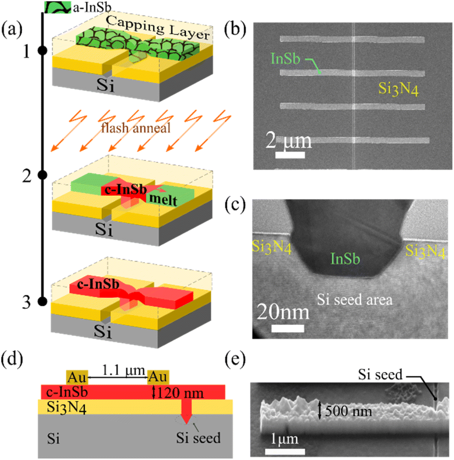 | ||
| Fig. 1 (a) Schematic overview of the RMG process. (1) Patterned amorphous InSb, in contact with the Si seed area and capped with a dielectric layer. (2) Flash annealing of the sample causing melting and rapid recrystallization of InSb starting from the seed area. (3) Schematic of the resulting crystalline InSb structure. (b) SEM image of the seed area and the InSb nanostructures before crystallization. (c) TEM cross sectional view of the Si seed area and InSb. (d) Schematic of the InSb detector (e) SEM image showing the InSb nanostructure used to make the photodetector. | ||
The recrystallized InSb nanostructures were characterized using electron back scatter diffraction (EBSD) and scanning electron microscope (SEM). The EBSD images were further analyzed using the MTex toolbox in Matlab.
To fabricate single nanostructure based InSb photodetectors, the recrystallized InSb nanostructures were contacted by Ni/Au electrodes formed in a lift-off process. The electrode separation is 1.1 μm with a device width of 500 nm. It is expected that an increase in width and decrease in length of the nanostructure could increase the photogenerated current. However, in this work we focus on a single device geometry. Studies have shown that GaSb nanostructures protected from oxidation using an oxide template resulted in higher mobility.28 Therefore, the Al2O3 capping layer was only removed in the contacted regions before metallization, leaving it to protect the InSb from oxidation elsewhere as oxidized InSb surfaces are known to contain a high density of defect states.29,30 Spectrally resolved photocurrent (PC) measurements were carried out at 77 K using Fourier transform infrared (FTIR) spectroscopy using a built-in globar IR source and KBr beam-splitter. We also recorded the time-response of the photodetector at 1550 nm by modulating the laser with a 1 Hz square wave using a pulse generator combined with a storage oscilloscope at different laser power.
Micro-Raman spectroscopy was performed using a Renishaw inVia Raman microscope with a 532 nm laser in a backscattering, unpolarized configuration. The laser was focused on the nanostructures with a microscope objective with numerical aperture NA = 0.85 and detected using a 3000 L mm−1 diffraction grating and a CCD camera. Reference spectra were collected from InSb (110) and (100) bulk crystal faces to establish the expected bulk TO and LO peak positions, respectively.
3 Results and discussion
3.1 Photoresponse
Fig. 2(a) presents the I–V characteristics of the MSM photodetector at room temperature (RT), where an ohmic behavior with no measurable difference between dark and illuminated conditions is observed. This is to be expected considering the narrow band gap of InSb, for which thermal carrier excitation will dominate the current transport at RT. From the known work function of Ni (5.25 V) and smaller electron affinity of InSb (4.59 eV) we can, in a first approximation, assume that a significant Schottky barrier should be present at the Ni–InSb junction, although the precise barrier height depends on the details of how the interface forms. By cooling the photodetectors to 77 K, thermal excitation is suppressed and indeed Schottky barriers at both contacts cause nonlinear I–V characteristics for which the current increases exponentially at low bias while at high bias the device responds in an ohmic fashion. Under these conditions we observe a clear response to illumination, with a difference of more than 2 orders of magnitude between the dark current and PC for positive biases (Fig. 2(b)). At high biases >0.4 V the forward-biased junction (J2) will be transparent due to the high voltage, while the reverse-biased junction (J1) will act as a constant series resistance set by the Schottky barrier height (Fig. 2(d)). Thus, by evaluating the temperature dependence of the I–V characteristics at large biases we can estimate the Schottky barrier height. The dark current for different temperatures is shown in Fig. 2(c). The dark current measured at 1 V falls by 3 orders of magnitude from 16.5 nA at 290 K to 10.6 pA at 140 K, after which the dark current stabilizes at 120 K and below. The barrier height of the metal–semiconductor contact was estimated using the Schottky diode equation in the following logarithmic form: | (1) |
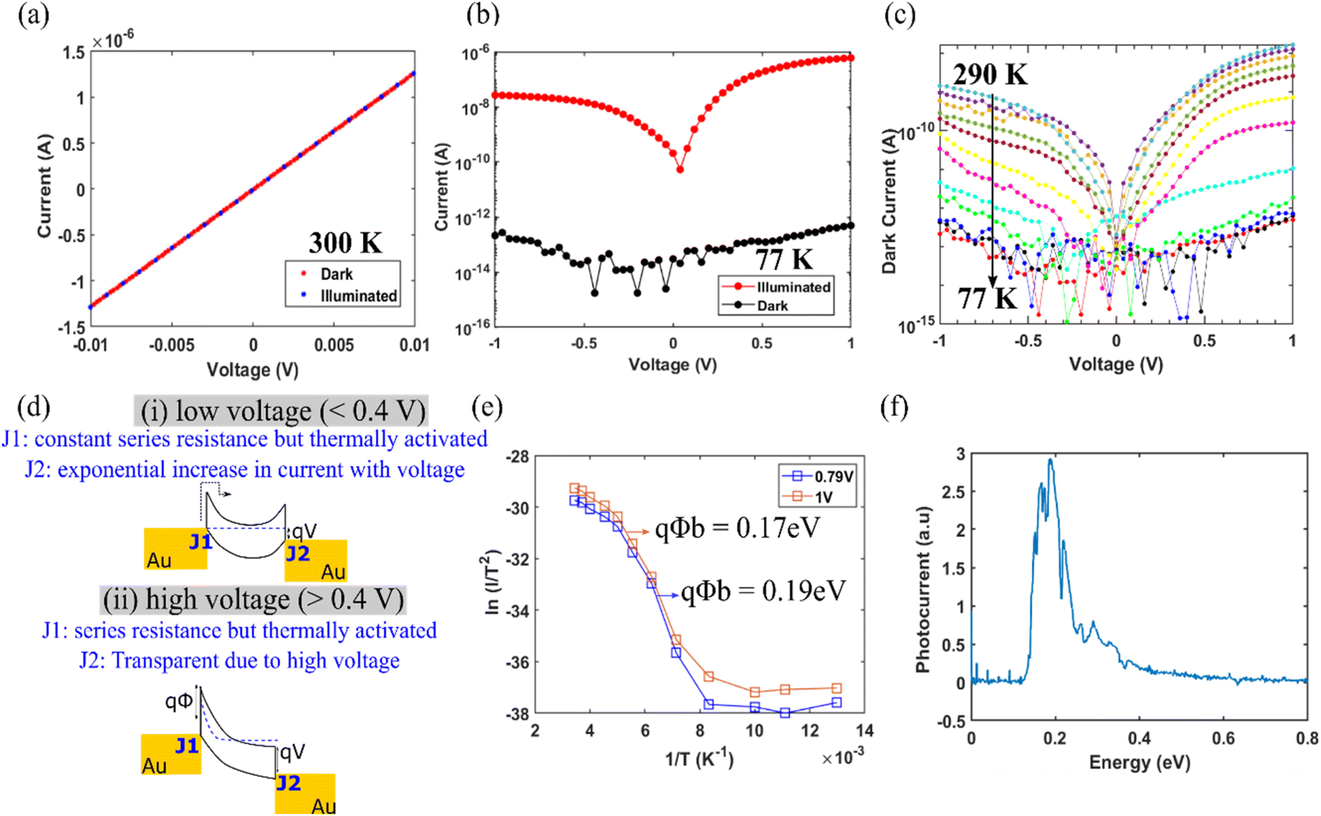 | ||
| Fig. 2 Current–voltage (I–V) curves of a single InSb nanostructure photodetector in dark and under illumination with a globar IR source at (a) 300 K and (b) 77 K. (c) Temperature-dependent I–V traces in dark. (d) Energy band diagram of the photodetector with indicated metal–semiconductor contacts. (e) Extraction of the Schottky barrier height at two different applied biases from the data in (c). (f) Spectrally resolved photocurrent. | ||
Next, FTIR PC spectroscopy was carried out to investigate the photoresponse of the InSb nanostructure photodetectors at 77 K. Fig. 2(f) shows the spectrally resolved PC. The expected bandgap of InSb at 77 K is around 0.23 eV and we do observe a peak in PC close to this energy (0.18 eV). However, the PC onset is redshifted to around 0.12 eV, thus significantly extending the photoresponsivity of the device out to 10 μm. The reason for this could be a bandgap narrowing induced by stress formed during the rapid crystallization of InSb from the melt in the RMG process, or the result of defect states near the conduction band edge.34 This is further investigated using EBSD in Section 3.3.
3.2. Photosensitivity
To explore the photosensitivity of the InSb MSM at 77 K, the device was illuminated with a calibrated 1550 nm diode laser. Fig. 3(a) presents the I–V characteristics for different laser power densities. For our measurements, the laser's optical output at a certain current was first measured using a power meter, while the power meter was covered with a cap with 1 mm2 hole in it. In this way we correlate the measured laser currents to optical power density (mW mm−2). As an example, a 100 mA corresponded to a power density of 19.5 mW mm−2. The distance between laser and the sample/power meter was kept constant throughout the experiments (measurement setup is shown in Fig. S3 in ESI†). The PC (Iph), defined as the increase in current under illumination, grows linearly with increasing laser power (Fig. 3(b)) over the investigated power density range. This allowed us to reliably extract the device responsivity from the measurement results. Responsivity (R) is the amount of output PC per incident optical power i.e., | (2) |
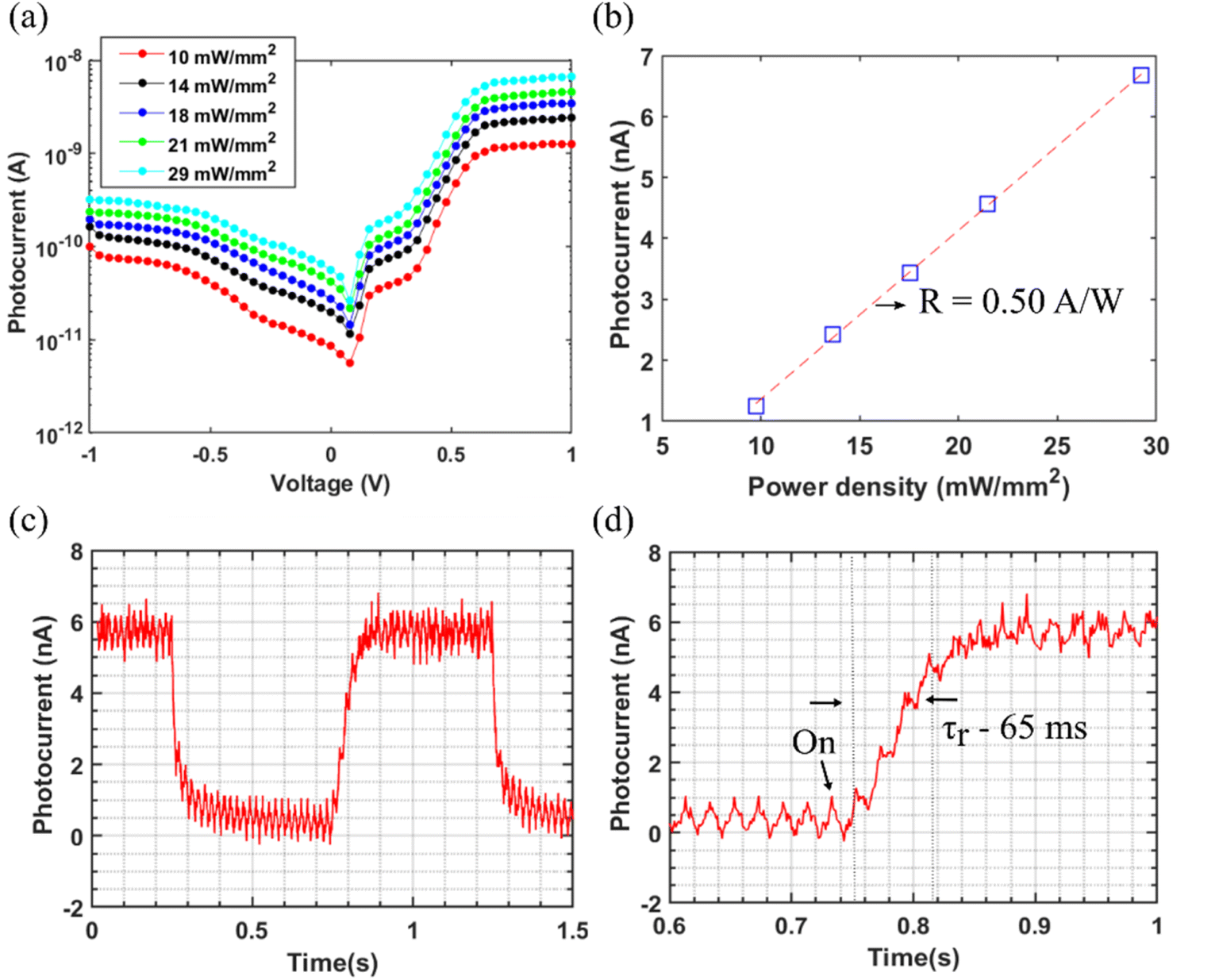 | ||
| Fig. 3 (a) I–V curves under 1550 nm illumination with different power densities at 77 K. Here, for instance the power density of 29 mW mm−2 corresponds to 16 nW power on a single photodetector element. (b) Dependence of PC on power density at 1 V bias. The slope of the plot corresponds to responsivity with consideration of device area. (c) Time-resolved PC response to a 1550 nm laser pulse train. (d) Time-resolved PC onset for the extraction of rise time. | ||
In this case, the responsivity extracted from the slope of Fig. 3(b) is 0.50 A W−1. Here we note that 29 mW mm−2 laser power density corresponds to 16 nW incident power onto the device. The PC variation with power density for different biases, as well as the variation of responsivity with bias, are given in the Fig. S4 and S5 in ESI.† Worth noting is that for all positive biases the responsivity remains nearly constant with varied illumination power, in contrast to many nanoscale photodetectors which report their highest responsivity values for ultralow power only. The previously reported single nanowire InSb photodetectors are of horizontal configuration in which the nanowires are transferred from the free-standing position to a lying position on another substrate horizontally.37 An InSb MSM photodetector fabricated using electrochemically synthesized InSb nanowires has been reported to have a responsivity of 8.4 × 10⁴ A W−1 (ref. 38) for an incident light at 5.5 μm at 0.49 mW cm−2. Our work involves direct integration of InSb detector on Si substrates, which has not been previously reported. Previous work on GaSb photodetectors fabricated using the RMG technique has reported a responsivity of 0.57 A W−1 for a power of 50 μW.39 A responsivity of 311 A W−1 at 4.3 μm for incident power of 1 pW was reported for an InSb nanosheet photodetector, while the responsivity at 100 pW was about ten times lower.35 Given our higher incident power (5–16 nW), the obtained responsivity values are thus reasonable. One limiting factor is the small device thickness (120 nm) which only absorbs about 20% of the incoming radiation at 1550 nm, estimated from the known absorption coefficient of InSb.40 In addition, we estimate that up to 40% of the incoming light could be reflected at the top surface, while reflection at the back InSb surface has only a marginal effect on responsivity (<10%). Future work may thus effectively optimize responsivity by engineered reflective coatings above and below the active InSb layer. Another limiting circumstance in the present case is that we do not have access to any quantum cascade laser operating at the bandgap of around 0.2 eV. By normalizing the spectrally resolved PC in Fig. 2(f) to optical power and using the know responsivity of 0.50 A W−1 at 1550 nm, we can estimate lower boundary of about 5 A W−1 at 6.1 μm.
Finally, we measure the response time of the photodetector using time-resolved PC measurements. Fig. 3(c) and (d) show the transient photoresponse under illumination with a modulated (1 Hz) 1550 nm diode laser @ 16 nW and 1 V bias. The rise and fall time of the detector is around 65 ms and 30 ms and is similar to or shorter than the reported values of the InSb nanosheet and InAs nanosheet photodetectors, which range from seconds to milliseconds.38,41,42 We do not observe response time in the nanosecond time scale as expected from diffusive transport transit time which can be explained by the large surface-to-volume ratio of our ultrathin device, causing delay of the photocurrent response through capture-emission processes via surface trap states. Although the intrinsic protection of the InSb surface is expected to provide some degree of surface passivation,28,43,44 further work will be needed to optimize the response speed of the photodetectors. In summary, our first experimental results for monolithically integrated InSb MSM photodetectors presented here indicate high responsivity in the MWIR spectrum (peak at 6.1 μm) and a relatively fast response speed and are thus promising for further work in this direction.
3.3. Crystallographic analysis
For monolithic InSb photodetectors formed by the RMG method to be a viable approach, we need to properly understand the crystallographic features that arise from the RMG process. Since we have observed a redshift in the spectrally resolved PC (Fig. 2(f)), indicating band gap narrowing that may be due to strain and/or crystal defects, we have invoked EBSD to carefully analyze the local crystalline properties of the InSb structures after the RMG process.![[1 with combining macron]](https://www.rsc.org/images/entities/char_0031_0304.gif) 11] direction. Therefore, we carefully analyze the domain orientations relative to each other. Having determined the mean orientation of the two types of domains, [349] (pink) and [829] (green), respectively, the first (pink) domain orientation is transformed by 60° rotation around the [11] axis. The stereographic projections of the transformed pink and original green lattices are presented in the Fig. S6 in ESI,† and perfectly coincides. This confirms the presence of discrete twin defects in the InSb structures. Twin defect formation is often observed in nanostructured growth of III–V semiconductor and is related to growth conditions variations like temperature instabilities, presence of impurities or morphological instability at the crystallization front.47–49 In-containing III–V semiconductors are sensitive to twin formation due to the relatively higher ionicity of the atomic bonds,50–52 while of these, InSb is least sensitive. In our work, the rather rough top surface of the crucible could disturb the growth front and contribute to the twin formation.
11] direction. Therefore, we carefully analyze the domain orientations relative to each other. Having determined the mean orientation of the two types of domains, [349] (pink) and [829] (green), respectively, the first (pink) domain orientation is transformed by 60° rotation around the [11] axis. The stereographic projections of the transformed pink and original green lattices are presented in the Fig. S6 in ESI,† and perfectly coincides. This confirms the presence of discrete twin defects in the InSb structures. Twin defect formation is often observed in nanostructured growth of III–V semiconductor and is related to growth conditions variations like temperature instabilities, presence of impurities or morphological instability at the crystallization front.47–49 In-containing III–V semiconductors are sensitive to twin formation due to the relatively higher ionicity of the atomic bonds,50–52 while of these, InSb is least sensitive. In our work, the rather rough top surface of the crucible could disturb the growth front and contribute to the twin formation.
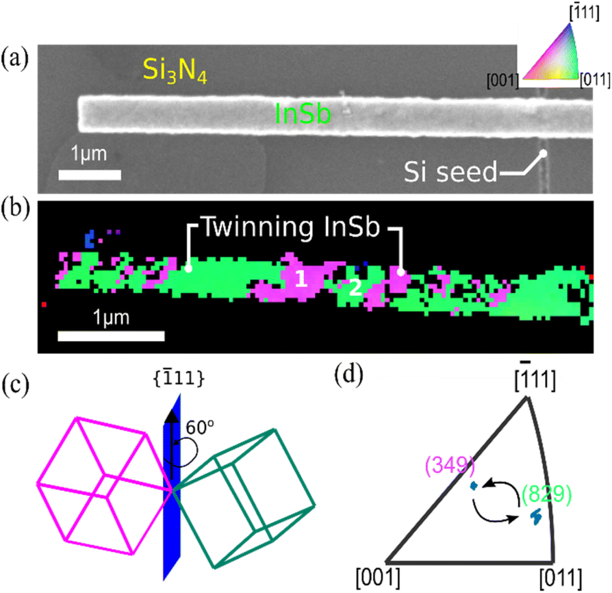 | ||
| Fig. 4 (a) SEM image of the analyzed InSb structure. (b) EBSD Z-orientation map of the InSb structure revealing repeated twin formation in the InSb crystal. 1 and 2 represents the domains used for the analysis. (c) Schematic representation of crystal rotation around [11] axis (d) inverse pole figure showing the two twinned domains. | ||
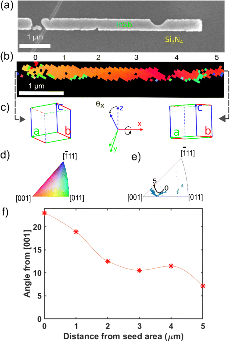 | ||
| Fig. 5 (a) SEM image of a flash annealed InSb nanostructure after removal of the capping layer. (b) The EBSD Z orientation of the InSb structure and (c) schematic representation of the crystal orientation at the beginning of the seed area and at the end of the seed area with the indication of rotation direction. (d) Colour-code for EBSD orientation map. (e) Inverse pole figure showing the lattice rotation. (f) Angular difference of different orientations of the InSb crystal with the (001) plane as a function of distance from Si seed area. | ||
The collected statistics on the out-of-plane InSb crystal orientations are presented in the inverse pole figure (IPF) in Fig. 6. Four specific crystallographic orientations [001], [113], [9 1 10], and [122] orientations are indicated with a specific color in the IPF map, for reasons that will be explained in the following. The intensity of the color extends to 5° outside the specific orientation. Here we can see that there are data points close to the [001] orientation (red in Fig. 6), which is same as the substrate, indicating that some nanostructures have a direct epitaxial relationship. The large lattice-mismatch between InSb and Si leads to the formation of dislocations at the heterojunction, and an inhomogeneous strain field at the heterointerface could thus easily cause a few degrees of crystal lattice tilt,65 which accounts for the spread of the data points around the [001] orientation. In addition, some degree of lattice rotation may already occur close to the seed area.
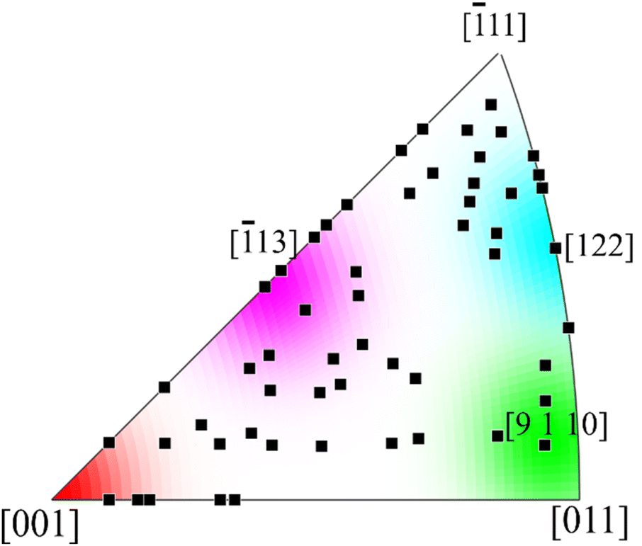 | ||
| Fig. 6 Orientation of InSb above the seed area extracted from EBSD Z orientation map for 55 structures and plotted on the inverse pole figure. Each orientation is associated with a specific color in the inverse pole figure. Here, few orientations are emphasized with the color coding extending to the vicinity of 5°. | ||
As we previously concluded that twin defects are often present in the InSb nanostructures, we should also see epitaxial but twinned domains having orientations close to [122] (cyan in Fig. 6). Indeed, we do see a clustering of data points close to this orientation.
However, the most prominent cluster of data rather has an orientation close to [113]. Previously, heteroepitaxial InSb films on Si (111) substrates were reported to be 30° rotated66 around the (111) axis which reduced the 19% lattice mismatch with Si to 3.3%.67 A similar study of InSb on V-groove Si (001) also reported the same 30° rotation of InSb films on <111> facets of the V-groove.68 Interestingly, rotation of [001] around a <111> axis at an angle of 30° yields <1 1.3 3.7> which is close to [113], suggesting that a similar effect could be present in our present work.
Of course, twinning of these rotated structures may also occur, which would result in orientations close to [9 1 10]. We can confirm the presence of structures with orientations close to this direction, shown as green in Fig. 6. In conclusion, we thus observe a complicated but epitaxial relationship between the crystal orientation of the InSb nanostructures and the Si substrate, the spread of the data indicating considerable residual strain. In addition, some data points fall outside this categorization, and we cannot exclude that some structures have grown in a non-epitaxial manner.
The variations in crystal orientation induced by the initial nucleation, twinning and lattice twist are not expected to have a direct effect on the photocurrent response of the InSb photodetectors, as the band structure of InSb is direct and symmetric around the Γ-point. However, an indirect effect could be that high-index facets on the top and bottom interface of the device may have higher surface recombination velocities than low index (001) or (110) surfaces.69 To evaluate this would be a topic for future studies.
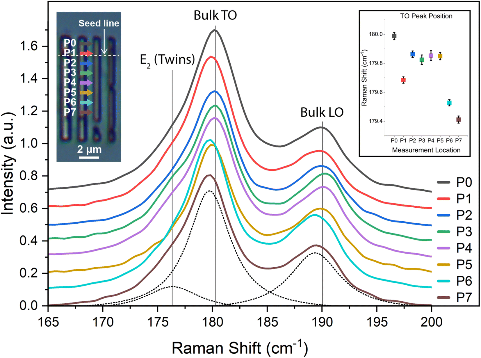 | ||
| Fig. 7 Raman spectra taken along a line scan of a 500 nm-wide InSb nanostructure. The top left optical micrograph inset shows the measurement locations. Vertical lines show the positions of the TO and LO Raman peaks as measured from a bulk InSb reference. The E2 peak is also indicated, which appears for wurtzite-like crystal structures, indicating the presence of twins. The spectrum for P7 is fitted to all three peaks, as shown by the dotted lines. The top right inset shows the fitted TO peak position and corresponding standard error at every point along the line scan. | ||
4. Conclusion
In conclusion, we have fabricated MSM single nanostructure InSb photodetectors monolithically integrated on Si using the RMG technique and analyzed their electrical and optical characteristics, together with their crystallographic properties at length. I–V measurements of the device at 77 K in dark and under illuminated conditions indicated more than 2 orders of magnitude difference in the photocurrent. Time-resolved photocurrent measurement using 1550 nm excitation demonstrated a response time of milliseconds, and a responsivity of 0.50 A W−1 at 16 nW, with extrapolated responsivity of 5 A W−1 at 6.1 μm wavelength. Spectrally resolved photocurrent measurements indicated a photocurrent onset below (0.12 eV) the expected bandgap of InSb (0.23 eV). This extends the photosensitivity of the device out to 10 μm and to find the origin of this led to further investigation of the crystallographic features formed in the single crystalline InSb during the RMG process. EBSD analysis of the InSb structures identified significant crystal twist, twins and evidence of local strain fields, which can explain the red shift of the photoresponse. The dominating crystal orientations indicate an epitaxial relationship to the Si substrate in most cases, which is complicated by the indications of crystal rotation at the onset of growth as well as occasional twinning. The presented results give an important insight into the potential and needs for further optimization to enable monolithically integrated InSb photodetectors on Si.Conflicts of interest
There are no conflicts to declare.Acknowledgements
This work is supported by Swedish Foundation for Strategic Research (nr ICA16-0008), Crafoord Foundation (nr 20171001), Royal Physiographic Society of Lund, and NanoLund. AFM and NM would also like to thank funding from SNSF though the NCCR QSIT and project No. CRSK-2_190289.References
- A. Rogalski, Infrared detectors: an overview, Infrared Phys. Technol., 2002, 43(3–5), 187–210 CrossRef.
- F. K. Tittel, A. A. Kosterev, Y. A. Bakhirkin, C. B. Roller, D. Weidmann and R. F. Curl, et al., Chemical sensors based on quantum cascade lasers, Proc. IEEE Sens., 2003, 2(2), 893–894 CAS.
- W. Fick, K. U. Gassmann, L. D. Haas, M. Haiml, S. Hanna and D. Hübner, et al., Infrared detectors for space applications, Adv. Opt. Technol., 2013, 2(5–6), 407–421 Search PubMed.
- B. W. Jia, K. H. Tan, W. K. Loke, S. Wicaksono, K. H. Lee and S. F. Yoon, Monolithic integration of InSb photodetector on silicon for mid-infrared silicon photonics, ACS Photonics, 2018, 5(4), 1512–1520 CrossRef CAS.
- R. Soref, Mid-infrared photonics in silicon and germanium, Nat. Photonics, 2010, 4(8), 495–497 CrossRef CAS.
- H. Lin, Z. Luo, T. Gu, L. C. Kimerling, K. Wada and A. Agarwal, et al., Mid-infrared integrated photonics on silicon: a perspective, Nanophotonics, 2017, 7(2), 393–420 Search PubMed.
- A. Spott, E. J. Stanton, N. Volet, J. D. Peters, J. R. Meyer and J. E. Bowers, Heterogeneous integration for mid-infrared silicon photonics, IEEE J. Sel. Top. Quantum Electron., 2017, 23(6), 8200810 Search PubMed.
- E. A. Plis, InAs/GaSb type-II superlattice detectors, Adv. Electron., 2014, 2014, 1–12 CrossRef.
- A. Rogalski, P. Martyniuk and M. Kopytko, InAs/GaSb type-II superlattice infrared detectors: future prospect, Appl. Phys. Rev., 2017, 4, 031304 Search PubMed.
- A. Rogalski, M. Kopytko and P. Martyniuk, Antimonide-based Materials. Antimonide-based Infrared Detect A New Perspect, 2018 Search PubMed.
- J. H. Lau, Recent advances and new trends in flip chip technology, J. Electron Packag. Trans. ASME, 2016, 138(3), 16–22 Search PubMed.
- R. Breiter, et al., Size, weight, and power reduction of mercury cadmium telluride infrared detection modules, Opt. Eng., 2011, 50(6), 061010 CrossRef.
- R. G. Driggers, et al., Infrared detector size: how low should you go?, Opt. Eng., 2012, 51(6), 063202 CrossRef.
- I. Kimukin, N. Biyikli and E. Ozbay, InSb high-speed photodetectors grown on GaAs substrate, J. Appl. Phys., 2003, 94(8), 5414–5416 CrossRef CAS.
- G. Singh, E. Michel, C. Jelen, S. Slivken, J. Xu and P. Bove, et al., Molecular-beam epitaxial growth of high quality InSb for p–i–n photodetectors, J. Vac. Sci. Technol. B: Microelectron. Nanometer Struct., 1995, 13(2), 782–785 CrossRef CAS.
- I. Kimukin, N. Biyikli, T. Kartaloǧlu, O. Aytür and E. Ozbay, High-speed InSb photodetectors on GaAs for mid-IR applications, IEEE J. Sel. Top. Quantum Electron., 2004, 10(4), 766–770 CrossRef CAS.
- E. Michel, J. Xu, J. D. Kim, I. Ferguson and M. Razeghi, InSb infrared photodetectors on Si substrates grown by molecular beam epitaxy, IEEE Photonics Technol. Lett., 1996, 8(5), 673–675 Search PubMed.
- H. Y. Serene Koh, Rapid Melt growth of Silicon Germanium for Heterogenous Integration on Silicon, Stanford University, 2011 Search PubMed.
- Y. Liu, M. D. Deal and J. D. Plummer, Rapid melt growth of germanium crystals with self-aligned microcrucibles on Si substrates, J. Electrochem. Soc., 2005, 152(8), G688 CrossRef CAS.
- H. Menon, N. P. Morgan, C. Hetherington, R. Athle, M. Steer and I. Thayne, et al., Fabrication of single-crystalline InSb-on-insulator by rapid melt growth, Phys. Status Solidi A, 2022, 219(4), 1–8 CrossRef.
- H. Menon, L. Södergren, R. Athle, J. Johansson, M. Steer and I. Thayne, et al., Improved quality of InSb-on-insulator microstructures by flash annealing into melt, Nanotechnology, 2021, 32, 165602 CrossRef CAS PubMed.
- Y. Liu, K. Gopalakrishnan, P. B. Griffin, K. Ma, M. D. Deal and J. D. Plummer, MOSFETs and high-speed photodetectors on Ge-on-insulator substrates fabricated using rapid melt growth, Tech. Dig. – Int. Electron Devices Meet., 2004, 100, 1001–1004 Search PubMed.
- X. Bai, C. Y. Chen, P. B. Griffin and J. D. Plummer, Si incorporation from the seed into Ge stripes crystallized using rapid melt growth, Appl. Phys. Lett., 2014, 104(5), 18–21 Search PubMed.
- J. Feng, R. Woo, S. Chen, Y. Liu, P. B. Griffin and J. D. Plummer, P-channel germanium FinFET based on rapid melt growth, IEEE Electron Device Lett., 2007, 28(7), 637–639 CAS.
- H. Y. S. Koh, S. L. Chen, P. B. Griffin and J. D. Plummer, High quality single-crystal laterally graded SiGe on insulator by rapid melt growth, Electrochem. Solid-State Lett., 2010, 13(8), 281–284 CrossRef.
- K. E. Hnida-Gut, M. Sousa, M. Hopstaken, S. Reidt, K. Moselund and H. Schmid, Electrodeposition as an alternative approach for monolithic integration of InSb on silicon, Front. Chem., 2022, 9, 1–8 RSC.
- H. Takeuchi, A. Wung, X. Sun, R. T. Howe and T. J. King, Thermal budget limits of quarter-micrometer foundry CMOS for post-processing MEMS devices, IEEE Trans. Electron Devices, 2005, 52(9), 2081–2086 CrossRef.
- M. Borg, H. Schmid, J. Gooth, M. D. Rossell, D. Cutaia and M. Knoedler, et al., High-mobility GaSb Nanostructures cointegrated with InAs on Si, ACS Nano, 2017, 11(3), 2554–2560 CrossRef CAS PubMed.
- J. L. Webb, J. Knutsson, M. Hjort, S. Gorji Ghalamestani, K. A. Dick and R. Timm, et al., Electrical and surface properties of InAs/InSb nanowires cleaned by atomic hydrogen, Nano Lett., 2015, 15(8), 4865–4875 CrossRef CAS PubMed.
- M. Baik, H. K. Kang, Y. S. Kang, K. S. Jeong, Y. An and S. Choi, et al., Electrical properties and thermal stability in stack structure of HfO2/Al2O3/InSb by atomic layer deposition, Sci. Rep., 2017, 7(1), 1–11, DOI:10.1038/s41598-017-09623-1.
- S. M. Sze and K. K. Ng, Physics of Semiconductor Devices, A John Wiley & Sons, Inc, Plublication. 2007. Available from: https://www.researchgate.net/publication/269107473_What_is_governance/link/548173090cf22525dcb61443/download%0A; http://www.econ.upf.edu/%7Ereynal/Civilwars_12December2010.pdf; https://think-asia.org/handle/11540/8282%0A; https://www.jstor.org/stable/41857625 Search PubMed.
- J. Wagner, A. L. Alvarez, J. Schmitz, J. D. Ralston and P. Koidl, Surface Fermi level pinning in epitaxial InSb studied by electric-field-induced Raman scattering, Appl. Phys. Lett., 1993, 63(3), 349–351 CrossRef CAS.
- H. Menon, L. Södergren, R. Athle, J. Johansson, M. Steer and I. Thayne, et al., Improved quality of InSb-on-insulator microstructures by flash annealing into melt, Nanotechnology, 2021, 32(16), 165602 CrossRef CAS PubMed.
- P. Sarangapani, Y. Chu and J. Charles, Non-equilibrium Green's function predictions of band tails and band gap narrowing in III–V semiconductors and nanodevices.
- S. Zhang, H. Jiao, X. Wang, Y. Chen, H. Wang and L. Zhu, et al., Highly sensitive InSb nanosheets infrared photodetector passivated by ferroelectric polymer, Adv. Funct. Mater., 2020, 1–8 Search PubMed 2006156:.
- Z. Liu, T. Luo, B. Liang, G. Chen, G. Yu and X. Xie, et al., High-detectivity InAs nanowire photodetectors with spectral response from ultraviolet to near-infrared, Nano Res., 2013, 6(11), 775–783 CrossRef CAS.
- Z. Li, J. Allen, M. Allen, H. H. Tan, C. Jagadish and L. Fu, Review on III–V semiconductor single nanowire-based room temperature infrared photodetectors, Materials, 2020, 13(6), 1400 CrossRef CAS PubMed.
- C. H. Kuo, J. M. Wu, S. J. Lin and W. C. Chang, High sensitivity of middle-wavelength infrared photodetectors based on an individual InSb nanowire, Nanoscale Res. Lett., 2013, 8(1), 1–8 CrossRef PubMed.
- Y. H. Chen, J. W. Jheng, P. Mishra, C. Y. Lin and M. C. M. Lee, GaSb MSM photodetectors on Si waveguides by rapid melt growth method, IEEE Photonics Technol. Lett., 2018, 30(11), 1013–1015 CAS.
- G. Gobeli and H. Y. Fan, Infrared absorption and valence band in indium antimonide, Phys. Rev., 1959, 1402, 613–620 Search PubMed.
- X. Wang, D. Pan, M. Sun, F. Lyu, J. Zhao and Q. Chen, High-performance room-temperature UV-IR photodetector based on the InAs Nanosheet and its wavelength-and intensity-dependent negative photoconductivity, ACS Appl. Mater. Interfaces, 2021, 13(22), 26187–26195 CrossRef CAS PubMed.
- S. Zhang, H. Jiao, X. Wang, Y. Chen, H. Wang, L. Zhu, W. Jiang, J. Liu, L. Sun, T. Lin, H. Shen, W. Hu, X. Meng, D. Pan, J. Wang, J. Zhao and J. Chu, Highly sensitive InSb nanosheets infrared photodetector passivated by ferroelectric polymer, Adv. Funct. Mater., 2020, 30, 2006156 CrossRef CAS.
- K. Toko, Y. Ohta, T. Sakane, T. Sadoh, I. Mizushima and M. Miyao, Single-crystalline (100) Ge networks on insulators by rapid-melting growth along hexagonal mesh-pattern, Appl. Phys. Lett., 2011, 98(4), 98–101 CrossRef.
- H. Schmid, M. Borg, K. Moselund, L. Gignac, C. M. Breslin, J. Bruley, D. Cutaia and H. Riel, Template-assisted selective epitaxy of III–V nanoscale devices for co-planar heterogeneous integration with Si, Appl. Phys. Lett., 2015, 106, 233101 CrossRef.
- K. Shimamura, Z. Yuan, F. Shimojo and A. Nakano, Effects of twins on the electronic properties of GaAs, Appl. Phys. Lett., 2018, 1–5 CAS 022105.
- H. J. Joyce, J. L. Boland, C. L. Davies, S. A. Baig and M. B. Johnston, A review of the electrical properties of semiconductor nanowires: insights gained from terahertz conductivity spectroscopy, Semicond. Sci. Technol., 2016, 31, 103003 CrossRef.
- K. Hulme and J. Mullin, Indium antimonide-a review of its preparation, properties and device applications, Solid State Electron., 1962, 5, 211–247 CrossRef CAS.
- D. T. J. Hurle and P. Rudolph, A brief history of defect formation, segregation, faceting, and twinning in melt-grown semiconductors, J. Crystal Growth, 2004, 264, 550–564 CrossRef CAS.
- F. Weinberg and C. Parfeniuk, Semiconductor invited review and optical crystal, 1995, 0008-4433(94).
- P. D. Kanungo, H. Schmid, M. T. Björk, L. M. Gignac, C. Breslin and J. Bruley, et al., Selective area growth of III–V nanowires and their heterostructures on silicon in a nanotube template: towards monolithic integration of nano-devices, Nanotechnology, 2013, 24(22), 225304 CrossRef PubMed.
- J. C. Phillips, Ionicity of the chemical bond in crystals, Rev. Mod. Phys., 1970, 42(3), 317–356 CrossRef CAS.
- P. Rudolph, Springer Handbook of Crystal Growth, 2010, pp. 159–201 Search PubMed.
- J. J. Wen, Z. Liu, L. Li, C. L. Li, C. Xue and Y. H. Zuo, et al., Cooling rate dependent lattice rotation in ge on insulators formed by rapid melt growth, ECS Solid State Lett., 2013, 2(9), 73–76 CrossRef.
- T. Tanaka, K. Toko, T. Sadoh and M. Miyao, High quality single-crystalline Ge-rich SiGe on insulator structures by Si-doping controlled rapid melting growth, Appl. Phys. Express, 2010, 3(3), 2–5 Search PubMed.
- R. Matsumura, Y. Tojo, M. Kurosawa, T. Sadoh, I. Mizushima and M. Miyao, Growth-rate-dependent laterally graded SiGe profiles on insulator by cooling-rate controlled rapid-melting-growth, Appl. Phys. Lett., 2012, 101, 241904 CrossRef.
- K. Toko, T. Tanaka, Y. Ohta, T. Sadoh and M. Miyao, Defect-free Ge-on-insulator with (100), (110), and (111) orientations by growth-direction-selected rapid-melting growth, Appl. Phys. Lett., 2010, 97(15), 95–98 CrossRef.
- K. Toko, Y. Ohta, T. Tanaka, T. Sadoh and M. Miyao, Chip-size formation of high-mobility Ge strips on SiN films by cooling rate controlled rapid-melting growth, Appl. Phys. Lett., 2011, 99(3), 1–4 CrossRef.
- D. J. Tweet, J. J. Lee, J. S. Maa and S. T. Hsu, Characterization and reduction of twist in Ge on insulator produced by localized liquid phase epitaxy, Appl. Phys. Lett., 2005, 87(14), 1–3 CrossRef.
- Z. I. Ozyurt, Development of a Large Area germanium on Insulator Platform by Liquid Phase Epitaxy, Middle East Technical University, 2017 Search PubMed.
- H. Yokoyama, Y. Ohta, K. Toko, T. Sadoh and M. Miyao, Growth-direction dependent rapid-melting-growth of Ge-On-insulator (GOI) and its application to Ge mesh-growth, ECS Trans., 2019, 35(5), 55–60 CrossRef.
- Z. Liu, J. Wen, T. Zhou, C. Xue, Y. Zuo and C. Li, et al., Lateral growth of single-crystal Ge on insulating substrate using amorphous Si seed by rapid melting growth, Thin Solid Films, 2015, 597, 39–43, DOI:10.1016/j.tsf.2015.11.025.
- S. Nakamura and T. Hibiya, Thermal conductivity of GaSb and InSb in solid and liquid states, J. Appl. Phys., 2001, 5125, 1–4 Search PubMed.
- R. G. Seidensticker and M. Rubenstein, Thermal conductivity of liquid InSb and liquid Ga, J. Appl. Phys., 1972, 43(2), 584–586 CrossRef CAS.
- C. P. Kuo, S. K. Vong, R. M. Cohen and G. B. Stringfellow, Effect of mismatch strain on band gap in III–V semiconductors, J. Appl. Phys., 1985, 57(12), 5428–5432 CrossRef CAS.
- C. V. Falub, M. Meduňa, D. Chrastina, F. Isa, A. Marzegalli and T. Kreiliger, et al., Perfect crystals grown from imperfect interfaces, Sci. Rep., 2013, 3(001), 1–6 Search PubMed.
- M. Mori, K. Nagashima, K. Ueda, T. Yoshida, C. Tatsuyama and K. Maezawa, et al., High quality InSb films grown on Si(111) substrate via InSb Bi-layer, e-J. Surf. Sci. Nanotechnol., 2009, 7, 145–148 CrossRef CAS.
- T. Ito, A. Kadoda, K. Nakayama, Y. Yasui, M. Mori and K. Maezawa, et al., Effective mobility enhancement in Al2O3/InSb/Si quantum well metal oxide semiconductor field effect transistors for thin insb channel layers, Jpn. J. Appl. Phys., 2013, 52(4 PART 2), 2–7 Search PubMed.
- M. Mori, S. Khamseh, T. Iwasugi, K. Nakatani, K. Murata and M. Saito, et al., InSb films grown on the V-grooved Si(001) substrate with InSb bilayer, Phys. Procedia, 2010, 3(2), 1335–1339, DOI:10.1016/j.phpro.2010.01.187.
- H. C. Sio, T. K. Chong, S. R. Surve, K. J. Weber and D. H. MacDonald, Characterizing the influence of crystal orientation on surface recombination in silicon wafers, IEEE J. Photovoltaics, 2016, 6(2), 412–418 Search PubMed.
- I. Zardo, S. Conesa-Boj, F. Peiro, J. R. Morante, J. Arbiol and E. Uccelli, et al., Raman spectroscopy of wurtzite and zinc-blende GaAs nanowires: polarization dependence, selection rules, and strain effects, Phys. Rev. B: Condens. Matter Mater. Phys., 2009, 80(24), 1–11 CrossRef.
- K. Aoki, E. Anastassakis and M. Cardona, Dependence of Raman frequencies and scattering intensities on pressure in GaSb, InAs, and InSb semiconductors, Phys. Rev. B: Condens. Matter Mater. Phys., 1984, 30(2), 681–687 CrossRef CAS.
Footnote |
| † Electronic supplementary information (ESI) available: Supplementary material contains more plots on Schottky barrier height, responsivity, and the analysis of twin structures in InSb crystal. See DOI: https://doi.org/10.1039/d2na00903j |
| This journal is © The Royal Society of Chemistry 2023 |