
 Open Access Article
 This Open Access Article is licensed under a Creative Commons Attribution-Non Commercial 3.0 Unported Licence
High p doped and robust band structure in Mg-doped hexagonal boron nitride
Lama
Khalil
a,
Cyrine
Ernandes
a,
José
Avila
b,
Adrien
Rousseau
c,
Pavel
Dudin
 b,
Nikolai D.
Zhigadlo
d,
Guillaume
Cassabois
c,
Bernard
Gil
c,
Fabrice
Oehler
a,
Julien
Chaste
a and
Abdelkarim
Ouerghi
*a
b,
Nikolai D.
Zhigadlo
d,
Guillaume
Cassabois
c,
Bernard
Gil
c,
Fabrice
Oehler
a,
Julien
Chaste
a and
Abdelkarim
Ouerghi
*a
aUniversité Paris-Saclay, CNRS, Centre de Nanosciences et de Nanotechnologies, 91120, Palaiseau, France. E-mail: abdelkarim.ouerghi@c2n.upsaclay.fr
bUniversité Paris-Saclay, Synchrotron SOLEIL, L'Orme des Merisiers, BP48, 91190 Saint-Aubin, France
cLaboratoire Charles Coulomb (L2C), Université de Montpellier, CNRS, 34095 Montpellier, France
dCrystMat Company, CH-8037, Zurich, Switzerland
First published on 6th April 2023
Abstract
In two dimensional materials, substitutional doping during growth can be used to alter the electronic properties. Here, we report on the stable growth of p-type hexagonal boron nitride (h-BN) using Mg-atoms as substitutional impurities in the h-BN honeycomb lattice. We use micro-Raman spectroscopy, angle-resolved photoemission measurements (nano-ARPES) and Kelvin probe force microscopy (KPFM) to study the electronic properties of Mg-doped h-BN grown by solidification from a ternary Mg–B–N system. Besides the observation of a new Raman line at ∼1347 cm−1 in Mg-doped h-BN, nano-ARPES reveals p-type carrier concentration. Our nano-ARPES experiments demonstrate that the Mg dopants can significantly alter the electronic properties of h-BN by shifting the valence band maximum about 150 meV toward higher binding energies with respect to pristine h-BN. We further show that, Mg doped h-BN exhibits a robust, almost unaltered, band structure compared to pristine h-BN, with no significant deformation. Kelvin probe force microscopy (KPFM) confirms the p-type doping, with a reduced Fermi level difference between pristine and Mg-doped h-BN crystals. Our findings demonstrate that conventional semiconductor doping by Mg as substitutional impurities is a promising route to high-quality p-type doped h-BN films. Such stable p-type doping of large band h-BN is a key feature for 2D materials applications in deep ultra-violet light emitting diodes or wide bandgap optoelectronic devices.
Layered two-dimensional (2D) materials are characterized by a strong anisotropy in the bonding energies along the crystal lattice directions.1 In the plane, the intra-layer bonding is mainly of the covalent type, while out-of-the plane weak interlayer interactions dominate, usually with an overwhelming van-der-Waals character.2 Most of the 2D compounds such as transition-metal dichalcogenides (TMDs) or hexagonal boron nitride (h-BN) can exist either in the bulk3,4 or as few- or mono-layer (ML).5 The ML form can often be obtained from the bulk through simple mechanical exfoliation, envisaged upon breaking the weak inter-layer bonding.
Similarly to their 3D counterparts, 2D materials commonly present structural defects that may significantly affect their physical and electronic properties.6 As in conventional 3D semiconductors, substitutional doping by chemical impurities is a promising way to tailor the electronic properties of 2D monolayers. For graphene, the direct substitution of carbon atoms in the honeycomb lattice by atoms with a different number of valence electrons generally affects the density of states. In such 2D carbon-based materials, nitrogen doping is a common practice, due to its comparable atomic size with carbon. Whether these N substitutions introduce electron-donor, electron-acceptor states, or neither of the two depends crucially on the local bond arrangements of the heteroatoms. In addition to bond configuration, dopant density can also dramatically change graphene physical properties, such as the electronic and magnetic characteristics.7–9 Hetero-atom substitution has also shown good results in other small band-gap 2D materials, such as TMDs.10–12 As for 3D semiconductors, substitutional doping is thus an efficient way to robustly tailor the material properties of many 2D materials, at the nanoscale. However we may expect more profound alterations of the electronic properties between intentionally doped and pristine (nominally undoped) 2D materials, due to the much reduced number of atoms in mono- or few-layer 2D compounds compared to their 3D counterparts.8,10–12
For large bandgap 2D material h-BN, chemical impurities can be introduced during or after growth. Recent experimental work on the Si or Mg doping of h-BN sheets,13 produced by Chemical Vapor Deposition (CVD), has shown the successful incorporation of Mg or Si heteroatoms in the h-BN lattice.14–16 However, a microscopic understanding of the local atomic and electronic structure induced by the substitutional doping process in h-BN is lacking, despite its wide usage in the scientific community. In particular, angle photoemission spectroscopy has not been performed on Mg-doped bulk h-BN, due to its relatively low electric conductivity compared to other 2D materials. In this context, we obtain here the direct visualization of the electronic band structure by angle-resolved photoemission spectroscopy (ARPES) in correlation with the Mg atomic density. Mg doping is obtained during the growth of h-BN crystals by solidification from a ternary Mg–B–N system using a high-pressure, high-temperature cubic anvil technique. Here, a mixture of Mg flakes (99.99% pure), amorphous B powder (99.99%) and amorphous BN powder (99.9%) in a molar ratio 1![[thin space (1/6-em)]](https://www.rsc.org/images/entities/char_2009.gif) :1.2:0.1 (total mass of ∼1 g) were used as starting materials and further enclosed in a BN crucible. The BN sources were purified before the use by heating them at 2000 °C for 2 h under dynamic vacuum in order to remove oxygen impurities and other volatile contaminants. In a typical growth run, the sample was compressed to 3 GPa at room temperature. Then the temperature was ramped up in 1 h to the value of ∼1900 °C, maintained there for 1 h, and finally cooled to 20 °C in 1 h. Afterwards, the pressure was released and the sample removed. Further details about the crystal growth process can be found elsewhere.17 To compensate for the lack of large-scale samples and to avoid the spatial averaging of areas with different stacking sequence18 or number of layers, we use nano-ARPES at synchrotron facility to restrict the h-BN analysis to homogenous nanometer-sized regions with well-controlled Mg concentrations. We then correlate the local electronic structure to density-functional theory (DFT) calculations, associated to microscopic Raman (μ-Raman) spectroscopy to obtain the local structural information. This combination of theoretical and experimental means allows for the unambiguous assignment of the different Mg-doped regions. Then the comparison between the experimental (ARPES) and calculated (DFT) band structure, shows that the position of the valence band maximum (VBM) is strongly correlated to the density of Mg atoms. The Mg doping does not deteriorate the experimental band structure, and ARPES in Mg doped h-BN gives rise to sharp bands with the usual π valence bands degenerate at the K point. Similarly, the h-BN crystal structure is not strongly affected by the Mg impurities and remains hexagonal, with the conventional AA′ stacking. Kelvin probe force microscopy (KPFM) confirms the doping, with a reduced Fermi level difference between pristine and Mg doped h-BN crystals.
:1.2:0.1 (total mass of ∼1 g) were used as starting materials and further enclosed in a BN crucible. The BN sources were purified before the use by heating them at 2000 °C for 2 h under dynamic vacuum in order to remove oxygen impurities and other volatile contaminants. In a typical growth run, the sample was compressed to 3 GPa at room temperature. Then the temperature was ramped up in 1 h to the value of ∼1900 °C, maintained there for 1 h, and finally cooled to 20 °C in 1 h. Afterwards, the pressure was released and the sample removed. Further details about the crystal growth process can be found elsewhere.17 To compensate for the lack of large-scale samples and to avoid the spatial averaging of areas with different stacking sequence18 or number of layers, we use nano-ARPES at synchrotron facility to restrict the h-BN analysis to homogenous nanometer-sized regions with well-controlled Mg concentrations. We then correlate the local electronic structure to density-functional theory (DFT) calculations, associated to microscopic Raman (μ-Raman) spectroscopy to obtain the local structural information. This combination of theoretical and experimental means allows for the unambiguous assignment of the different Mg-doped regions. Then the comparison between the experimental (ARPES) and calculated (DFT) band structure, shows that the position of the valence band maximum (VBM) is strongly correlated to the density of Mg atoms. The Mg doping does not deteriorate the experimental band structure, and ARPES in Mg doped h-BN gives rise to sharp bands with the usual π valence bands degenerate at the K point. Similarly, the h-BN crystal structure is not strongly affected by the Mg impurities and remains hexagonal, with the conventional AA′ stacking. Kelvin probe force microscopy (KPFM) confirms the doping, with a reduced Fermi level difference between pristine and Mg doped h-BN crystals.
Nano-ARPES requires a highly conductive substrate, and the substrate must not affect the electronic dispersion of the Mg-doped h-BN material studied here. A possible solution consists in the mechanical transfer of the h-BN material on a monocrystalline epitaxial graphene layer grown on SiC. Here, the thermal decomposition of undoped 4H-SiC(0001) at 1550 °C in 800 mbar argon for 10 min was used to produce a large and uniform graphene film with a long-range order and high electron mobility. The graphene characteristic and thicknesses can be tuned by varying different experimental parameters.19,20Fig. 1(a) presents schematic of the full sample structure, with the layered Mg-doped h-BN being transferred on the graphene/SiC substrate. Our Mg-doped h-BN multilayers are obtained by mechanical exfoliation of a bulk crystal by the standard scotch tape technique. Fig. 1(b) sketches the conventional crystal structure of hexagonal (2H) h-BN, referred as the AA′ stacking (or polytype). Each individual layer of h-BN consists in boron B and nitrogen N atoms arranged in the two inequivalent A and B sublattices of the hexagonal lattice. In the presented crystal structure each B atom is stacked on a N atom and reciprocally (AA′ stacking). From previous experiments and literature, we then expect the in-plane BN and BB bond lengths to be about 1.45 and 2.52 Å, respectively.20 Similarly, the expected interlayer spacing of bulk h-BN is 3.33 Å.21 The graphene underlayer only interacts with the h-BN by weak van-der-Waals interactions. The graphene/SiC surface guarantees a reduced strain on multilayer h-BN, and is known to have a negligible impact on the h-BN band structure and the Fermi energy level.22 An optical micrograph of the sample is shown in Fig. 1(c), with several large homogenous h-BN domains spanning several tens of microns. Note that the sample underwent an annealing at 300 °C under ultra-high vacuum (UHV) conditions to remove any contamination between the graphene and h-BN layers.
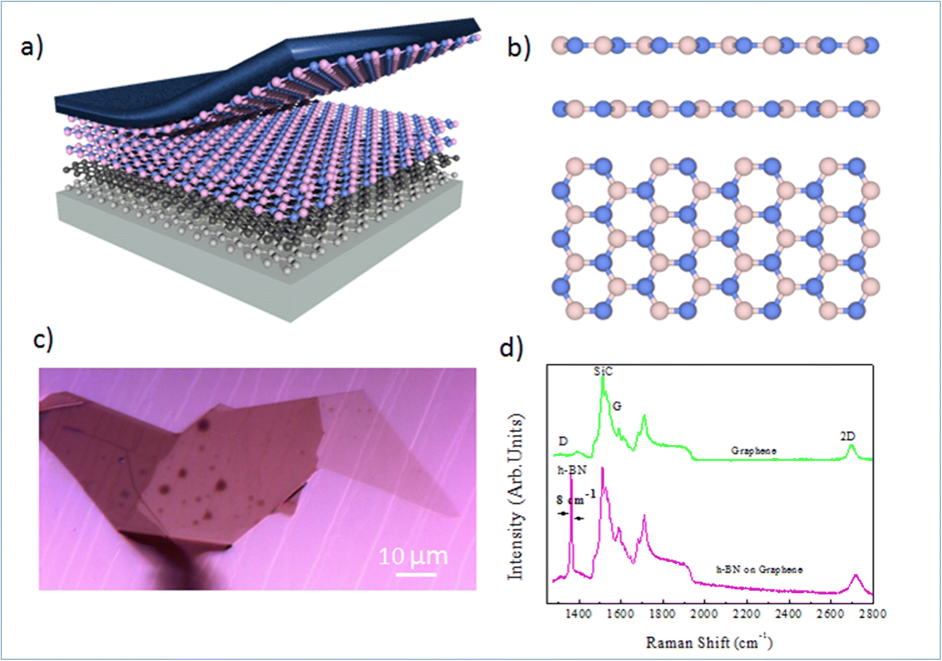 | ||
| Fig. 1 Crystal structure and micro-Raman spectroscopy of multilayer Mg doped h-BN: (a) graphical representation of the mechanical exfoliation of the h-BN sample on the graphene/SiC surface. (b) Crystal structure of the 2H (AA′) h-BN polytype. (c) Optical image of the Mg-doped h-BN sample, as exfoliated on graphene/SiC surface. (d) Micro-Raman spectra of h-BN/graphene and reference graphene area (532 nm laser, room temperature). | ||
To learn more about the electronic properties and confirm the incorporation of Mg in h-BN, we first perform micro-Raman spectroscopy. This technique is widely used to study 2D materials and allows to determine the number and the stacking sequence of layers, as well as the presence of external electrical field, doping and strain. Fig. 1(d) shows typical micro-Raman spectra of the Mg doped h-BN/graphene and pristine graphene/SiC layer in the wavenumber range of 1350–3000 cm−1, obtained at room temperature using a 532 nm laser. We first look at the reference graphene/SiC spectra (green curve). Besides the second-order Raman bands from the SiC substrate (1200 cm−1), the main three Raman modes of graphene are present: (i) the D band (defect induced mode, 1370 cm−1), (ii) the G band (in-plane vibration mode, 1550 cm−1) and (iii) the 2D band (two-phonon mode, 2710 cm−1), which are the standard hallmarks of a quality graphene layer. Comparing to the h-BN/graphene heterostructure spectra (pink), we observe a new peak at 1365 cm−1. This characteristic feature corresponds to the in-plane vibration (E2g) of B and N atoms in the h-BN crystal.23–25 The line widths (7–8 cm−1) of this BN-related peak (1365 cm−1) is obtained from the full width at half maximum (FWHM) after fitting to pure Lorentzian shape. The D peak of graphene (1350 cm−1), which is sensitive to the defects in graphene or induced by its surrounding, shows no evolution between pristine graphene and h-BN/graphene heterostructure, which evidences the quality of the van-der-Waals interface and validates our transfer protocol. The persistence of this graphene 2D peak in the heterostructure confirms the lack electronic states at the interface and indicates that the graphene and h-BN layers are nearly fully decoupled electronically.
In Fig. 2, we focus on the BN-related Raman signal around 1365 cm−1. Fig. 2(a) compares different Raman spectra from Mg-doped h-BN/graphene with reference undoped h-BN.26 The spectra are normalized to the intensity of the standard E2g stretching mode of the B and N atoms, at 1365 cm−1 in h-BN.23–25 In addition to this well-identified line, visible in both the reference and Mg-doped h-BN layers, we observe a new satellite peak near 1347 cm−1, which only appears in Mg-doped h-BN. The linewidth, position and intensity of this Raman signal vary as a function of the position on the sample (see zones 1 to 3 in Fig. 2). As this new peak correlates to the presence of Mg in h-BN grown by solidification from a ternary Mg–B–N system, we hypothesize it stems from a local perturbation induced by the Mg-related impurities in the h-BN crystal. Any atomic substitution with different charge, ionic mass or radius either introduces new local vibration modes, or leads to spectral shifts of the existing modes due to increased or decreased bond length. Here, the redshift suggests a direct incorporation of the Mg-atoms in the h-BN lattice, forming relatively longer Mg–N bonds after the substitution of boron atoms.16Fig. 2(b) and (c) present Raman intensity maps of the 1365 cm−1 and 1347 cm−1 Raman lines, respectively. The spatial localization of zones 1–3 used to acquire the individual spectra of Fig. 2(a) is also indicated. Atomic force microscopy demonstrates that the optical contrast of Fig. 1(c) arises from thickness variations of our multilayer h-BN sample (zone 1: 46 nm, zone 2: 41 nm, zone 3: 17 nm). These thickness variations directly translate into the observed intensity changes of the E2g-Raman line at 1365 cm−1 (Fig. 2(b)), and also affects the Mg-related peak map (Fig. 2(c)). Comparatively, the Mg-related map (Fig. 2(c)) presents larger spatial fluctuations in area of constant thickness, which hints at local inhomogeneities of the Mg incorporation in the h-BN crystal. Some Mg-doped h-BN crystals were further analyzed by transmission electron microscopy (TEM). This TEM sample was prepared as follow. First Mg-doped BN flakes were exfoliated from the bulk crystal and transferred to a SiO2/Si surface for Raman measurement (similar to Fig. 2(a) red curve). After verification of the characteristic Mg-doped h-BN Raman lines (see above), selected flakes were then transferred to a conventional copper TEM grid using a PMMA method. The TEM and scanning TEM (STEM) observations were performed on a FEI Titan Themis operating at 200 kV. The chemical composition of the material was measured by Energy Dispersive X-rays Spectroscopy (EDX) using a calibrated Bruker “Super X” detector. In Fig. 2(d), we see the EDX composition of a representative area. As the Mg-doped BN flakes are overwhelmingly composed of B and N, we use a logarithmic scale so that the other chemical elements are visible on the same graph. We observe a Cu signal (from the TEM grid) and a SiO signal (from residual SiO2 picked up by the PMMA transfer). The Mg signal is visible but at the limit of detection of our equipment. Quantification of the B, N and Mg signal reveals atomic composition xB = 49.94%, xN = 50.05% and xMg = 0.01% with xB + xN + xMg = 100%. Given the low (but visible) Mg signal, this measurement is very imprecise and we estimate that the actual Mg concentration is comprised between 0.01 and 0.05%. Considering an atomic density of 1.1 × 10²³ at. cm−3 for h-BN, we deduce a Mg atomic density between 1 × 10²⁰ and 5 × 10²⁰ at. cm−3. The Fig. 2(e) shows an atomically resolved STEM image of the h-BN lattice viewed along the [0001] zone axis. The atomic lattice is well resolved and shows a clear hexagonal structure with no visible defect. The TEM diffraction, Fig. 2(e) (inset), confirms the crystal phase to be hexagonal.
 | ||
| Fig. 2 Room temperature micro-Raman spectroscopy of Mg doped h-BN: (a) micro-Raman spectra of Mg-doped and reference pristine h-BN crystals. The spatial positions of zones 1–3 are shown in (b). (b) and (c) Micro-Raman peak position maps of the Mg-doped h-BN sample integrated around 1365 cm−1 and 1347 cm−1, respectively. Excitation wavelength is 532 nm for all Raman data, (d) EDX spectra of the Mg-doped h-BN flakes transferred on a TEM grid. The Mg signal is about 3 orders of magnitude lower than the B and N contribution, (e) atomically resolved STEM image along the [0001] zone axis, showing the hexagonal BN lattice. The corresponding TEM diffraction is shown in the inset, exposing a clear hexagonal signature. | ||
We now turn to the study of Mg-doping on the electronic structure of h-BN with nano-ARPES. In Fig. 3, we compare the band structure of pristine h-BN to that of Mg-doped h-BN. The corresponding electronic dispersions, Fig. 3(a and b), are collected along the high symmetry ΓK direction. The π and σ bands of h-BN20 are easily identified in both samples. On the one hand, the π states disperse from the Γ point up towards the valence band maximum (VBM) located at the K point in the ΓK direction, then down to the M point in the KM direction (not shown). On the other hand, the σ bands, degenerate at the Γ point, disperse downwards to the K point.27 The main change from pristine (Fig. 3(a)) to Mg-doped hBN (Fig. 3(b)) is an upshift of the VBM from 2.98 eV (pristine h-BN) binding energy (BE), to 2.83 eV BE (Mg-doped h-BN) (Fig. 3(c)). In order to fully understand each electronic band structure, we superpose in Fig. 3(d and e) our experimental ARPES data with band structure calculations in the DFT framework for free standing (undoped) h-BN layer of hexagonal symmetry (AA′ stacking) using PBE functionals. The only modification required to obtain a good fit is an energy shift of the DFT calculated bands to account for the different Fermi level position. All main features are well reproduced by the calculated band structures, for both the pristine and Mg-doped h-BN. Considering that our DFT model is strictly hexagonal AA′ h-BN, the good match between the experimental and simulated band structure hints at a standard hexagonal crystal structure for Mg-doped h-BN (AA′ stacking), consistent with previous experimental studies and theoretical predictions.20,27 From the ARPES data, Fig. 3, the incorporation of Mg impurities has a profound but uniform effect on the overall electronic properties of the h-BN crystal. As seen from the DFT comparison, Fig. 3(c and d), the energy shift measured on π band occurs uniformly over the whole band structure. Therefore, it behaves just as a global shift of the valence bands toward the Fermi-level, aka. conventional p-type doping. This experimental p-type doping of our Mg-containing h-BN layer can be explained by a charge transfer from Mg atoms to the h-BN layer. Mg-doped h-BN thus exhibits a robust, almost unaffected, band structure with no significant band deformation over the probed k-space.
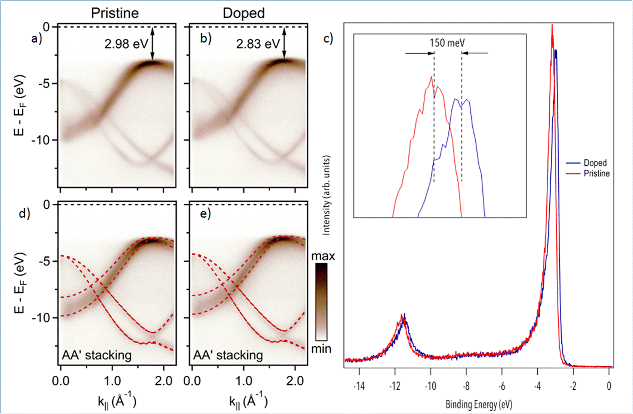 | ||
| Fig. 3 Electronic structure of pristine and Mg doped h-BN: (a and b) nano-ARPES spectra of pristine h-BN and Mg-doped h-BN acquired at photon energy hν = 100 eV, respectively. (c) Nano-ARPES intensity integrated spectra as a function of the binding energy, extracted from the 2D ARPES map, for pristine h-BN (red line) and Mg-doped h-BN (blue line). (d and e) Same nano-ARPES data with superposed band structure from DFT calculation (PBE) of bulk hexagonal AA′ h-BN. | ||
To confirm the doping in our Mg-doped h-BN, we use correlative AFM and KPFM to quantitatively analyze the changes in surface potential between our Mg-doped h-BN sample and a reference pristine (nominally undoped) h-BN sample. Fig. 4(a and b) show the AFM topography of the hBN crystal (light color) on top of the graphene/SiC substrate (dark color). The thickness of the pristine h-BN is about 23.0 nm, comparable to that of zone 3 of our Mg-doped sample. Fig. 4(c and d) present the KPFM surface potential map of the selected samples. Due to the difference of the work function between graphene and h-BN, clear surface potential difference is observed, leading to the observed contrast between the graphene substrate (dark color) and the h-BN crystal (light color) in the KPFM data. The work function of graphene layer is about 4.3 eV this implies that the work function of Mg doped h-BN is about 4.4 eV. Spatial fluctuations in Fig. 4(c) possibly relates to local inhomogeneities of the Mg incorporation in the h-BN crystal, as already observed in Raman map at a larger scale (Fig. 2(c)). To quantify the value of the surface potential across the h-BN/graphene junction, we extract representative line profiles in Fig. 4(e and f). A clear increase of surface potential between the pristine and the Mg-doped h-BN from 100 to 190 ± 10 mV can be measured, demonstrating a large Fermi-level variation in the Mg-doped h-BN and the p-doping character of the Mg atoms.
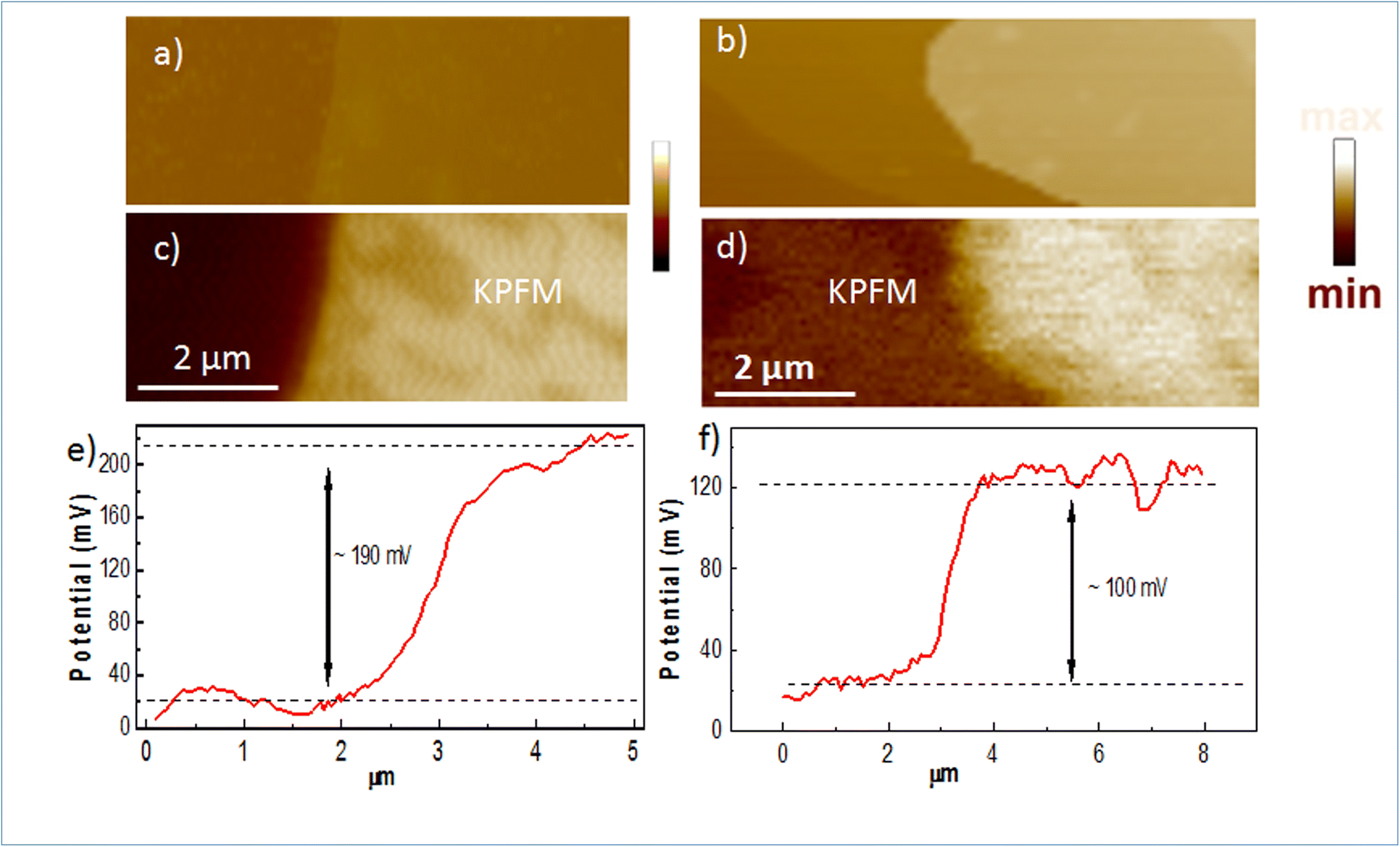 | ||
| Fig. 4 Surface potential of pristine and Mg doped h-BN deposited on graphene: (a and b) AFM images of the pristine and Mg-doped h-BN. Lateral scale is the same than KPFM images. (c and d) Corresponding KPFM images. (e and f) KPFM line profiles taken perpendicularly to the h-BN/graphene interface. | ||
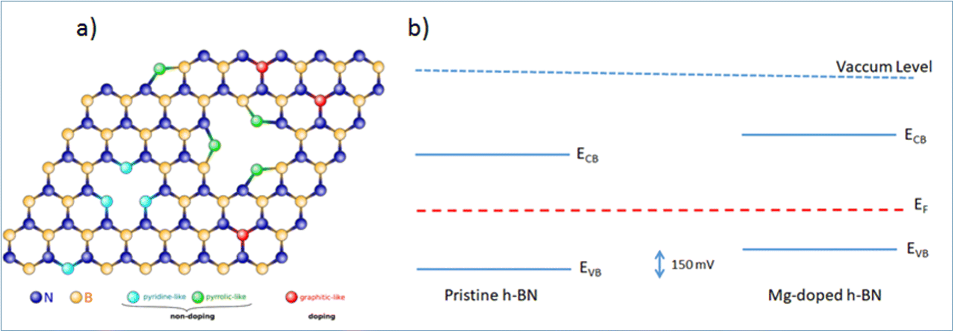
While the simple substitution of B by Mg is an option, alternative structural models can be proposed for the incorporation of Mg in the h-BN honeycomb lattice. Due to the structural proximity between h-BN and graphene, we draw here a parallel between n-type doped graphene and nitrogen N impurities8,28 and we identify three main configurations: ‘graphitic’, ‘pyridine-like’ and ‘pyrrolic-like’ (Fig. 5(a)). ‘Graphitic’ magnesium is a direct substitution, in which the Mg atom simply replaces a host boron atom B. Since Mg is over coordinated in this arrangement this configuration is expected to act as an electron acceptor and contribute electrically to the observed p-type doping.16 Alternatively, ‘pyridine-like’ Mg is the collective replacement of three nitrogen N atoms by three Mg atoms in a triangular arrangement. In this configuration, each Mg only bonds to two other atoms (B and N) and should not bear any additional electrical charge. Similarly, ‘pyrrolic-like’ Mg is the collective replacement of three BN pairs by three Mg atoms in a triangular symmetry. Here also, each Mg only bonded to two atoms should bear not extra electron. Therefore, we expect that both ‘pyrrolic-like’ and ‘pyridine-like’ Mg should not contribute electrically to the p-type doping, leaving the ‘graphitic’ boron-substituted Mg as the main contributor to the experimental p-type doing. Other study on Mg-doping of h-BN considering another type of defect also concludes on the predominance of such ‘graphitic’ Mg substitution.16 In particular, it showed that the single Mg substitution is the only configuration presenting a Mg–N bond length longer than the original B–N bond length, thus being the only one in agreement with the Raman peak red-shift associated with the Mg substitution of Fig. 1(d). On the basis of these results, we are able to determine all the respective band offsets of pristine and Mg doped h-BN. Considering the known values of the quasiparticle bandgaps for h-BN we obtain a valence band discontinuity ΔEv = 0.15 ± 0.02 eV (Fig. 5(b)). The KPFM (∼90 mV) and ARPES (∼150 meV) upshifts are comparable and we attribute the difference to the spatial inhomogeneities of the Mg incorporation. This result evidences the p type doping effect in the Mg doped h-BN sample.
 | ||
| Fig. 5 (a) Proposed atomic arrangements of Mg impurities in h-BN of the three suggested Mg incorporation sites: graphitic, pyrrolic, and pyridinic. The crystal is viewed along the c-axis. (b) Band alignment and offset in our h-BN/graphene heterostructures, as determined from the ARPES data. | ||
In summary, we have successfully conducted high-resolution nano-ARPES experiments from high-quality exfoliated Mg-doped h-BN crystals. Our experimental results coupled with theoretical calculations show that the stacking order for multilayer Mg-doped h-BN is AA′. We find that such Mg-doped h-BN gives rise to sharp electronic bands, in particular for the valence bands at the K point, which linewidth compares favorably to those from reference pristine h-BN. The incorporation of Mg atoms does not change the experimental band structure and we retrieve all the hallmarks of pristine h-BN with degenerate π bands at the K point. The main feature of Mg-doped h-BN is a collective up shift of the valence bands, which is well resolved experimentally, and which demonstrates the presence of an effective p-type doping as a shift of the Fermi level in the Mg-doped h-BN.
Conflicts of interest
There are no conflicts to declare.Acknowledgements
We thank Christophe David for the KPFM measurement and Gilles Patriarche for the STEM measurement. We acknowledge the financial support by MagicValley (ANR-18-CE24-0007) and Graskop (ANR-19-CE09-0026), 2D-on-Demand (ANR-20-CE09-0026), and MixDferro (ANR-21-CE09-0029) grant. This work is also supported by a public grant overseen by the French National Research Agency (ANR) as part of the “Investissements d'Avenir” program (Labex NanoSaclay, ANR-10-LABX-0035) and by the French technological network RENATECH. We thank Cristine Giorgetti for the h-BN band structure calculation.References
- A. K. Geim and K. S. Novoselov, The rise of graphene, Nat. Mater., 2007, 6, 183–191 CrossRef CAS PubMed.
- A. K. Geim and I. V. Grigorieva, Van der Waals heterostructures, Nature, 2013, 499, 419–425 CrossRef CAS PubMed.
- G. Cassabois, P. Valvin and B. Gil, Hexagonal boron nitride is an indirect bandgap semiconductor, Nat. Photonics, 2016, 10, 262–266 CrossRef CAS.
- T. Q. P. Vuong, et al., Phonon-Photon Mapping in a Color Center in Hexagonal Boron Nitride, Phys. Rev. Lett., 2016, 117, 1–5 CrossRef.
- R. Bourrellier, et al., Nanometric Resolved Luminescence in h-BN Flakes: Excitons and Stacking Order, ACS Photonics, 2014, 1, 857–862 CrossRef CAS.
- D. Pierucci, et al., Van der Waals epitaxy of two-dimensional single-layer h-BN on graphite by molecular beam epitaxy: electronic properties and band structure, Appl. Phys. Lett., 2018, 112, 253102 CrossRef.
- M. Boutchich, et al., Atmospheric pressure route to epitaxial nitrogen-doped trilayer graphene on 4H-SiC (0001) substrate, Appl. Phys. Lett., 2014, 105, 233111 CrossRef.
- D. Usachov, et al., Nitrogen-doped graphene: efficient growth, structure, and electronic properties, Nano Lett., 2011, 11, 5401–5407 CrossRef CAS PubMed.
- E. Velez-fort, et al., Epitaxial Graphene on 4H-SiC (0001) Grown under Nitrogen Flux : Evidence of Low Nitrogen Doping and High, ACS Nano, 2012, 10893–10900 CrossRef CAS PubMed.
- T. D. Thanh, et al., Recent advances in two-dimensional transition metal dichalcogenides-graphene heterostructured materials for electrochemical applications, Prog. Mater. Sci., 2018, 96, 51–85 CrossRef CAS.
- D. Pierucci, et al., Tunable Doping in Hydrogenated Single Layered Molybdenum Disulfide, ACS Nano, 2017, 11, 1755–1761 CrossRef CAS PubMed.
- P. Mallet, et al., Bound Hole States Associated to Individual Vanadium Atoms Incorporated into Monolayer WSe2, Phys. Rev. Lett., 2020, 125, 1–6 CrossRef.
- S. Lu, et al., Towards n-type conductivity in hexagonal boron nitride, Nat. Commun., 2022, 13, 1–10 CAS.
- S. Majety, T. C. Doan, J. Li, J. Y. Lin and H. X. Jiang, Electrical transport properties of Si-doped hexagonal boron nitride epilayers, AIP Adv., 2013, 3, 122116 CrossRef.
- A. Mballo, et al., Towards p-type conduction in hexagonal boron nitride: doping study and electrical measurements analysis of HBN/algan heterojunctions, Nanomaterials, 2021, 11, 1–12 CrossRef PubMed.
- F. Sun, et al., P-Type conductivity of hexagonal boron nitride as a dielectrically tunable monolayer: modulation doping with magnesium, Nanoscale, 2018, 10, 4361–4369 RSC.
- N. D. Zhigadlo, Crystal growth of hexagonal boron nitride (hBN) from Mg-B-N solvent system under high pressure, J. Cryst. Growth, 2014, 402, 308–311 CrossRef CAS.
- J. Zribi, et al., Structural and electronic transitions in few layers of isotopically pure hexagonal boron nitride, Phys. Rev. B, 2020, 102 DOI:10.1103/PhysRevB.102.115141.
- E. Pallecchi, et al., High electron mobility in epitaxial graphene on 4H-SiC(0001) via post-growth annealing under hydrogen, Sci. Rep., 2014, 4 DOI:10.1038/srep04558.
- H. Henck, et al., Direct observation of the band structure in bulk hexagonal boron nitride, Phys. Rev. B, 2017, 95, 085410 CrossRef.
- X. Blase, A. Rubio, S. G. Louie and M. L. Cohen, Quasiparticle band structure of bulk hexagonal boron nitride and related systems, Phys. Rev. B, 1995, 51, 6868–6875 CrossRef CAS PubMed.
- H. Henck, et al., Stacking fault and defects in single domain multilayered hexagonal boron nitride, Appl. Phys. Lett., 2017, 110, 023101 CrossRef.
- H. Sediri, et al., Atomically Sharp Interface in an h-BN-epitaxial graphene van der Waals Heterostructure, Sci. Rep., 2015, 5, 16465 CrossRef CAS PubMed.
- S. Liu, et al., Single Crystal Growth of Millimeter-Sized Monoisotopic Hexagonal Boron Nitride, Chem. Mater., 2018, 30, 6222–6225 CrossRef CAS.
- S. M. Kim, et al., Synthesis of large-area multilayer hexagonal boron nitride for high material performance, Nat. Commun., 2015, 6, 8662 CrossRef CAS PubMed.
- H. Henck, et al., Direct observation of the band structure in bulk hexagonal boron nitride, Phys. Rev. B, 2017, 95, 085410 CrossRef.
- R. J. Koch, et al., Electronic structure of exfoliated and epitaxial hexagonal boron nitride, Phys. Rev. Mater., 2018, 2, 074006 CrossRef CAS.
- E. Vélez-Fort, E. Pallecchi, M. G. Silly, M. Bahri, G. Patriarche, A. Shukla, F. Sirotti and A. Ouerghi, Single step fabrication of N-doped graphene/Si3N4/SiC heterostructures, Nano Res., 2014, 7, 835–843 CrossRef.
| This journal is © The Royal Society of Chemistry 2023 |