
 Open Access Article
 This Open Access Article is licensed under a Creative Commons Attribution-Non Commercial 3.0 Unported Licence
Atomic scale insights into the epitaxial growth mechanism of 2D Cr3Te4 on mica†
Hailin
Yang
,
An
Wu
,
Huaxin
Yi
,
Weiwei
Cao
 ,
Jiandong
Yao
,
Guowei
Yang
and
Yi-Chao
Zou
*
,
Jiandong
Yao
,
Guowei
Yang
and
Yi-Chao
Zou
*
School of Materials Science & Engineering, State Key Laboratory of Optoelectronic Materials and Technologies, Nanotechnology Research Center, Sun Yat-sen University, Guangzhou, 510275, P. R. China. E-mail: zouych5@mail.sysu.edu.cn
First published on 15th December 2022
Abstract
Two-dimensional (2D) magnetic materials are of wide research interest owing to their promising applications in spintronic devices. Among them, chromium chalcogenide compounds are some of the limited available systems that present both high stability in air and high Curie temperatures. Epitaxial growth techniques based on chemical vapour deposition (CVD) have been demonstrated to be a robust method for growing 2D non-layered chromium chalcogenides. However, the growth mechanism is not well-understood. Here, we demonstrate the epitaxial growth of Cr3Te4 nanoplates with high quality on mica. Atomic-resolution scanning transmission electron microscopy (STEM) imaging reveals that the epitaxial growth is based on nanosized chromium oxide seed particles at the interface of Cr3Te4 and mica. The chromium oxide nanoparticle exhibits a coherent interface with both mica and Cr3Te4 with a lattice mismatch within 3%, suggesting that, as a buffer layer, chromium oxide can release the interfacial strain, and induce the growth of Cr3Te4 although there is a distinct oxygen-content difference between mica and Cr3Te4. This work provides an experimental understanding behind the epitaxial growth of 2D magnetic materials at the atomic scale and facilitates the improvement of their growth procedures for devices with high crystalline quality.
Introduction
2D magnetic materials are of great research importance in the key fields of spintronics, topological physics and materials science.1–5 In 1966, the Mermin–Wagner theorem proposed that the isotropic Heisenberg model does not exist for 2D long-range magnetic ordering at non-zero temperatures because of thermal fluctuations.6 It was not until the recent findings of intrinsic ferromagnetism in CrI3 and CrGeTe3,7,8 researchers started to realize that magnetic anisotropy can eliminate this limitation which allows Ising ferromagnetism.2,8,9 With this development, 2D magnetic materials have attracted extensive attention for spintronic and magnetic storage devices.10,11 However, most 2D magnetic materials like CrI3 are unstable under the ambient environment, limiting their practical applications.12 Therefore, it is of technological importance to develop air-stable 2D magnetic materials.Among the air-stable 2D magnetic materials, chromium chalcogenide compounds exhibit a very high Curie temperature over room temperature,13–18 making them appealing for spintronic devices. For example, ferromagnetism can hold above 300 K in a metallic phase of 1T-CrTe2 down to the atomically thin limit.13,16 On the other hand, 2D chromium–telluride (Cr–Te) compounds are some of the very-limited 2D magnetic materials that have shown exotic phenomena such as anomalous Hall effects and the topological Hall effect.15,19–21 Furthermore, with a low-symmetry crystal structure and strong spin–orbit coupling, Cr–Te compounds offer a unique platform for studying magnetocrystalline anisotropy.22,23 The unique magnetic properties and abundant spin phenomena make 2D Cr–Te compounds an excellent candidate for spintronic devices.
Various preparation methods for growing Cr–Te compounds have been employed in recent years, including mechanical exfoliation, molecular beam epitaxy and CVD.24–27 Cr–Te films with few layers grown by molecular beam epitaxy have demonstrated inherent long-range ordered ferromagnetism.18,24,25 Compared to mechanical exfoliation and molecular beam epitaxy, CVD shows advantages in the phase engineering and possibility of wafer-scale production with low cost.5,26,27 Previous studies have shown that almost all the available materials in the Cr–Te system can be grown by CVD, including CrTe,27–29 Cr2Te3,30,31 Cr5Te8,21,26 Cr3Te4,19 and CrTe2.32 Through changing the growth parameters during CVD, the phase structure and stoichiometric ratio of Cr–Te compounds can be adjusted. For example, through tuning the growth temperature, Meng et al. found that the thickness of 1T-CrTe2 nanosheets can be reduced to several nanometers from ∼130 nm, along with a monotonic increase of the Curie temperature. Tang et al.21 realized phase engineering of Cr5Te8 nanosheets with a colossal anomalous Hall effect through controlling the cooling rate. These advantages make CVD a commonly used method for the synthesis of 2D chromium–telluride compounds.
Achieving the synthesis of high-quality non-layered Cr–Te compound crystals, such as Cr5Te8 and Cr3Te4, is still a challenge. It is remotely possible to use conventional exfoliation methods to obtain non-layered 2D Cr–Te, as their interlayer binding is not solely based on van der Waals interactions (referred to as ‘non-layered’)19 and therefore comparatively strong compared to the layered ones like CrTe2, due to the existence of covalent bonding formed between the intercalated Cr atoms with surrounding Te atoms. Until now, CVD has been the only robust method reported that can successfully grow non-layered Cr–Te compounds.21,26–29 For example, recently Li et al. demonstrated the growth of ultrathin air-stable Cr3Te4 nanosheets with topologically nontrivial magnetic-spin states.19 In fact, many of the 2D magnetic materials are achieved by an epitaxial growth on mica.33 Wu et al.29 obtained CrTe crystals with mono- and few unit-cell thickness through a CVD-assisted epitaxial growth. Chen et al. synthesized highly air-stable Cr5Te8 nanosheets on mica, where all the grown nanosheets showed well aligned side facets, suggesting a feature of epitaxial growth.26 However, no work has yet been done on the epitaxial growth mechanism of 2D magnetic materials, although such a procedure has already been widely employed. This prompts the need for studies to clarify the growth mechanism and to fill the research gap in the controllable growth of 2D magnetic crystals with high quality.
In this study, we demonstrate an epitaxial growth of Cr–Te nanoplates on mica by CVD and investigate the epitaxial interfaces using advanced electron-microscopy. Through careful structural and compositional analysis, we found that the interfacial structures are more complicated than expected: instead of a direct stack of hexagonal Cr or Te atomic rings on mica's Si–Al–O pseudo-hexagonal rings, the interface of Cr3Te4 and mica is oxygen-rich with nanosized Cr2O3 seed particles. Specifically, through detailed structural investigation using the sub-angstrom STEM technique, the crystallographic orientation relationships between different phases and their formation mechanisms have been investigated.
Experimental
Sample growth
Cr3Te4 nanoplates were grown on mica substrates based on an atmospheric pressure CVD system using a quartz tube with a diameter of one inch. CrCl3 (Aladdin, anhydrous, 99.9% metals basis) powder and Te powder (Sigma Aldrich, 200 mesh, 99.8% trace metals basis) were used as the Cr and Te sources. Prior to the growth, the mica substrate was freshly cleaved so that a clean surface was exposed for sample growth. During the CVD growth, a quartz boat containing a mixed powder of CrCl3 and Te (weight ratio of CrCl3![[thin space (1/6-em)]](https://www.rsc.org/images/entities/char_2009.gif) :Te ∼ 0.1) was placed at the central region of the CVD furnace. The mica substrate was placed face down on this quartz boat for the sample growth and deposition. A mixed gas of argon and hydrogen (Ar:H2 = 95:5 vol%) with a flow rate of 100 sccm was used as the carrier gas throughout the process. For a typical growth, the growth temperature was set as 660–700 °C with a ramp rate of 40–50 °C min−1 and held for 8 min at the growth temperature. Once the growth was complete, the top cover of the furnace was opened for a rapid cooling. The lateral size of the nanoplate can be increased to ∼25 μm by employing a tube-in-tube growth technique (see ESI Fig. S1†).26
:Te ∼ 0.1) was placed at the central region of the CVD furnace. The mica substrate was placed face down on this quartz boat for the sample growth and deposition. A mixed gas of argon and hydrogen (Ar:H2 = 95:5 vol%) with a flow rate of 100 sccm was used as the carrier gas throughout the process. For a typical growth, the growth temperature was set as 660–700 °C with a ramp rate of 40–50 °C min−1 and held for 8 min at the growth temperature. Once the growth was complete, the top cover of the furnace was opened for a rapid cooling. The lateral size of the nanoplate can be increased to ∼25 μm by employing a tube-in-tube growth technique (see ESI Fig. S1†).26
Characterization
Scanning electron microscopy (SEM) was conducted using a Hitachi Regulus 8230 with a cold-field emission gun, equipped with a Bruker Quantax X-ray energy-dispersive spectrometer (EDS). Atomic force microscopy (AFM) characterization was performed using a Bruker Dimension FastScan microscope operated in a tapping mode. X-ray diffraction (XRD) was conducted using a Rigaku D/Max-2200 VPC system with an operational X-ray tube power of 1.6 kW and a Cu Kα was used as the X-ray source. Raman spectra were obtained using a confocal Renishaw inVia Raman microscope equipped with a 532 nm laser. The laser was focused on the sample with a 50× objective. The power of laser excitation measured below the microscope objective lens was set to 2.25 mW to ensure signal acquisition. All measurements were performed at room temperature. Transmission electron microscopy (TEM) characterization techniques, including bright-field (BF) imaging and selected area electron diffraction (SAED), were carried out on an FEI Tecnai F30 microscope operated at 300 kV. Atomic-resolution STEM images were acquired from an aberration-corrected STEM FEI Titan Themis 60-300, operated at 300 kV using an annular dark field (ADF) detector with a collection angle of ∼48–200 mrad and a BF detector. To reduce the electron-beam damage on the mica substrate, we used a probe current of ∼9 pA for high resolution imaging under a low dose34 and a probe current of ∼40 pA for EDS acquisition. Multi-slice image simulations for high resolution STEM images were conducted using QSTEM software and a source size of 0.8–1 Å. Cross-sectional TEM specimens were prepared using a focused ion beam-scanning electron microscope (FIB SEM, FEI Helios 660) by 30 kV, 16 kV, 5 kV and 2 kV ion beam milling and polishing to electron transparency.Results and discussion
Fig. 1 shows the morphological and compositional characterization results of the as-grown products. We found that the as-grown nanostructures display a morphology of hexagonal nanoplates (see Fig. 1b). These nanoplates are of several to tens of micrometers in lateral size, with well-defined side facets and flat surfaces. Interestingly, we note that the crystallographic edges of the as-grown nanoplates are parallel to each other, suggesting that there is an epitaxial relationship between the substrate and the as-grown nanoplates. In order to obtain details of the sample morphological and structural information, we conducted AFM, Raman, EDS and XRD characterization. Statistical AFM measurement shows that the nanoplates have a thickness ranging from 10–150 nm, depending on the growth temperature (Fig. S1†). For the sample in Fig. 1b, a typical AFM height profile is shown in Fig. 1d and e, showing a nanoplate with a thickness of ∼60 nm with a clean and flat surface. The atomically flat surface indicates that there was no observable screw dislocation formed during the nanoplate growth. Fig. 1f presents a Raman spectrum taken from the nanoplates, which displays two main characteristic peaks located at 117 and 137 cm−1, corresponding to the out-of-plane A1g and in-plane Eg vibrational modes of chromium chalcogenides, consistent with previous reports.21,27 To confirm the compositional uniformity within the nanoplates, we carried out an EDS mapping on single nanoplates with SEM (Fig. 1g–i). A quantitative and statistical analysis of the EDS spectra gives a Cr atomic ratio of 44 at% in Cr–Te with an uncertainty of ±2 at%, suggesting a Cr-rich phase, very close to the theoretical atomic ratio of Cr in Cr3Te4 of ∼42.9 at%. EDS mapping also shows that the Cr and Te elements are distributed evenly within the nanoplates, as shown in Fig. 1j. Fig. 1k shows the corresponding XRD patterns taken from the as-grown samples on mica, which display both the peaks from the nanoplates (orange) and the peaks from the mica substrate (grey). The peaks from the mica substrate match the powder diffraction file (PDF, # 01-084-1305) from a typical muscovite KAl3Si3O10(OH)2 with a space group of C2/c(15). The XRD pattern from the samples matches well with the standard peaks from Cr3Te4 according to the XRD database (PDF # 04-003-4548, with a = 6.85 Å, b = 3.92 Å, and c = 12.27 Å, and a space group of C2/m(12)). Therefore, the above characterization results confirm that our nanoplates have a composition of a Cr–Te compound and a high crystallinity.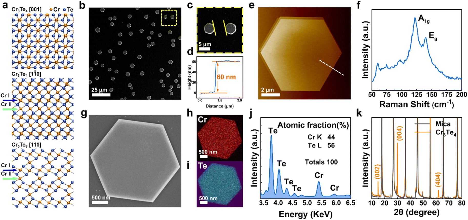 | ||
Fig. 1 (a) A schematic showing the crystal structure of Cr3Te4 viewed along different zone axes, with the top panel for [001] and the middle panel for [1![[1 with combining macron]](https://www.rsc.org/images/entities/char_0031_0304.gif) 0]. Bottom panel shows a comparison to Cr5Te8 viewed along [110]. (b) An over-view SEM image showing the as-grown hexagonal nanoplates on the mica substrate. (c) A magnified SEM image magnified from the area denoted by a yellow-dashed rectangle in (b), with the two lines illustrating that the nanoplates have crystallographic edges that are parallel to each other. (d) An AFM height profile taken from a sample section marked by a white dashed line in (e), showing a thickness of ∼60 nm. (e) Corresponding AFM image. (f) A typical Raman spectrum taken from the nanoplate, showing two characteristic peaks at around 117 cm−1 and 137 cm−1. (g) A magnified SEM image showing the regulated shape and flat surface of the nanoplate. (h and i) Corresponding EDS maps taken from the sample with Cr and Te maps displayed in (h and i) respectively. (j) An EDS spectrum showing the Cr and Te characteristic peaks from the sample with a quantitative analysis result shown in the top right corner. (k) XRD patterns taken from the sample, where the orange pattern is from the sample whereas the grey pattern is from the blank mica substrate. 0]. Bottom panel shows a comparison to Cr5Te8 viewed along [110]. (b) An over-view SEM image showing the as-grown hexagonal nanoplates on the mica substrate. (c) A magnified SEM image magnified from the area denoted by a yellow-dashed rectangle in (b), with the two lines illustrating that the nanoplates have crystallographic edges that are parallel to each other. (d) An AFM height profile taken from a sample section marked by a white dashed line in (e), showing a thickness of ∼60 nm. (e) Corresponding AFM image. (f) A typical Raman spectrum taken from the nanoplate, showing two characteristic peaks at around 117 cm−1 and 137 cm−1. (g) A magnified SEM image showing the regulated shape and flat surface of the nanoplate. (h and i) Corresponding EDS maps taken from the sample with Cr and Te maps displayed in (h and i) respectively. (j) An EDS spectrum showing the Cr and Te characteristic peaks from the sample with a quantitative analysis result shown in the top right corner. (k) XRD patterns taken from the sample, where the orange pattern is from the sample whereas the grey pattern is from the blank mica substrate. | ||
To determine the crystal structure of our nanoplates, we conducted electron diffraction characterization using TEM. Among the possible Cr–Te phases to be determined for our nanoplates, we note that Cr5Te8 and Cr3Te4 can show similar {001} peak positions in XRD, while most of the nanoplates lie on the substrates with dominant {001} surface planes, which makes only the {001} peaks ‘visible’. However, Cr5Te8 and Cr3Te4 do show distinct differences in atomic stacking when viewed along 〈110〉 directions (see middle and bottom panels of Fig. 1a), for which we need a view perpendicular to their {001} planes. Therefore, we conducted cross-sectional (S)TEM imaging to examine the phase structure. The cross-sectional (S)TEM samples were prepared using FIB (see the Experimental section), and the FIB lamellae were cut parallel to the crystallographic edges of the nanoplates. Fig. 2a shows an over-view image of our cross-sectional sample, in which the middle region is the sample, below which the dark area is the mica substrate. To determine the phase of the sample, we performed SAED from the Cr–Te (denoted as CT) area along three zone axes, by rotating the sample along the 〈001〉 axis. Fig. 2b shows the SAED pattern taken from the sample area without rotation. From Fig. 2b, the diffraction spots along the out-of-plane direction show an atomic-plane spacing of ∼6.08 Å, which can be indexed to the {002} plane of Cr3Te4. Using a similar approach, we can index the other diffraction spots in Fig. 2b, and therefore the zone axis of this SAED can be determined to be [1![[3 with combining macron]](https://www.rsc.org/images/entities/char_0033_0304.gif) 0]CT. Subsequently, we rotated the sample along the 〈001〉 axis by ∼12° and ∼30° respectively and obtained two other sets of electron diffractions, as shown in Fig. 2c and d, which can be indexed to the [1
0]CT. Subsequently, we rotated the sample along the 〈001〉 axis by ∼12° and ∼30° respectively and obtained two other sets of electron diffractions, as shown in Fig. 2c and d, which can be indexed to the [1![[2 with combining macron]](https://www.rsc.org/images/entities/char_0032_0304.gif) 0] and [10] axes of Cr3Te4 respectively. The tilt angle between those zone axes matches well with the angle between the corresponding axes of Cr3Te4 (i.e. ∼12° tilt from [10] to [10], and ∼30° tilt from [10] to [10], see Fig. 2b–d). Therefore, the phase structure of our nanoplate samples can be initially identified as Cr3Te4.
0] and [10] axes of Cr3Te4 respectively. The tilt angle between those zone axes matches well with the angle between the corresponding axes of Cr3Te4 (i.e. ∼12° tilt from [10] to [10], and ∼30° tilt from [10] to [10], see Fig. 2b–d). Therefore, the phase structure of our nanoplate samples can be initially identified as Cr3Te4.
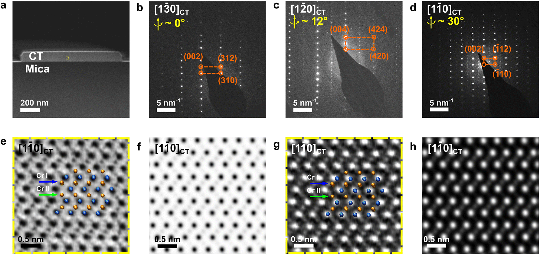 | ||
| Fig. 2 (a) An overview ADF-STEM image showing the cross-sectional TEM sample on the mica substrate. (b–d) SAED patterns taken from the nanoplate along various zone axes, obtained from a crystal tilt of ∼0° (b), ∼12° (c) and ∼30° (d). (e) Experimental BF-STEM image taken from the sample, magnified from the area denoted by a yellow square in (a). (f) Corresponding simulated image at [10]CT. (g) High resolution ADF-STEM experimental image and (h) corresponding simulated image at [10]CT. Insets in (e) and (g) display the positions of Cr (orange balls) and Te (dark blue balls) atomic columns. | ||
To further confirm the atomic-stacking sequence in the as-grown nanoplates, we conducted atomic-resolution STEM imaging under ADF-STEM and BF-STEM modes along the [10] axis. It should be pointed out that there are two distinct Cr coordinates in the non-layered Cr–Te. As shown in Fig. 1a, the crystal structure of the non-layered Cr–Te can be considered as such that, between the CrTe2 layers (Cr I), there are intercalated Cr atoms (Cr II). Here we defined those two types of Cr coordinates, as Cr I, and Cr II, as illustrated by the atomic models in Fig. 1a. The difference between Cr3Te4 and Cr5Te8 is in the number of intercalated Cr atoms. In Cr3Te4, the ratio between the number of atoms occupied at Cr II:Cr I is 50 at% and Cr II is fully occupied. In contrast, the atomic ratio of Cr II:Cr I is much less, and 25 at% in Cr5Te8, where Cr II is not fully occupied (Fig. 1a). Therefore, experimental STEM images can directly distinguish if the phase is Cr3Te4 or Cr5Te8 by checking the occupation at Cr II sites in our samples. Fig. 2e and f show the BF-STEM images taken from the sample, where the dark dots indicate the presence of atoms. We can clearly see that the Cr II coordinates are fully occupied by Cr (Fig. 2e), in agreement with our simulated BF-STEM image for [10]CT in Fig. 2f. Fig. 2g shows the corresponding ADF-STEM image taken from our samples. We can find that the positions of atomic columns (bright contrast) are consistent with the projection of the atomic model under this axis. Please note that the intensity in an ADF-STEM image is approximately proportional to the atomic number Z1.7, while the atomic numbers of Te and Cr are 72 and 24, respectively. The intensity of the intercalated Cr layers is therefore small in ADF-STEM images (Fig. 2g and h), due to a smaller number of Cr atoms in Cr II compared to Cr I, as well as a much lower atomic number of Cr compared to Te, confirmed by the simulated ADF-STEM image in Fig. 2h. Thus, due to the fact that the Cr II coordinates are fully occupied in our samples, the as-grown nanoplate is composed of a single-crystalline Cr3Te4 phase instead of Cr5Te8.
To understand the epitaxial relationship between the Cr3Te4 nanoplates and the mica, we note that during the electron diffraction experiments for Cr3Te4 (Fig. 2), the mica substrate is also very close to the zone axis, when we viewed the sample along the [10]CT axis. This suggests that the epitaxial relationship between the two can be found around this zone axis. Fig. 3a shows the SAED pattern taken from both the Cr3Te4 sample and its underlying mica, in which two sets of diffraction patterns are superimposed, with one belonging to [10]CT and the other indexed to [010]Mica. The analysis of Fig. 3a suggests that, besides the expected {001}Mica//{001}CT resulting from a layer-by-layer growth, there is another crystallographic relationship being {60}Mica//{420}CT. The crystallographic relationships between the sample and the mica suggest that there exist coherent interfaces between them. To investigate if this is indeed the case, we further conducted atomic-resolution ADF-STEM imaging along the [10]CT axis. Interestingly, we found that a ‘buffer layer’ with a thickness of only a few nanometers was formed between the nanoplate and the substrate, which was not noticeable without high-resolution imaging. This ‘buffer layer’ is composed of dispersed seed particles that are aligned along the interfaces. Fig. 3b presents an ADF-STEM image showing a typical seed particle, through which we can see that the buffer layer exhibits a slightly lower brightness compared to Cr3Te4, while still brighter than the bottom mica substrate, suggesting a different composition compared to Cr3Te4 or mica. In order to characterize the composition of the buffer layer, we conducted an EDS line scan along the out-of-plane direction, across the interface of mica/seed particle and the seed particle/Cr3Te4 interface (see the bottom panel of Fig. 3b). A quantitative analysis of the EDS scan through the center region of the seed particle shows that the seed particle has a chemical composition of ∼60 at% O and ∼40 at% Cr with an uncertainty of ±4 at%. The EDS result indicates that the intermediate layer is probably composed of chromium oxide Cr2O3. To confirm this, we further took atomic-resolution ADF-STEM images from the seed nanoparticle to resolve its crystal structure, as shown in Fig. 3c and d. Combining this image and its fast Fourier transform (FFT) images (Fig. 3g and h), we found that the FFT pattern from the seed particle area can be indexed to the [241] zone axis of a trigonal Cr2O3 phase (PDF # 04-002-5942, with a = b = 4.96 Å, and c = 13.80 Å, and a space group of Rc(167)).
 | ||
| Fig. 3 (a) A typical SAED pattern taken from the Cr3Te4–mica interface, containing two sets of patterns with one indexed to the [010]Mica zone axis and the other to [10]CT zone axis. (b) An ADF-STEM taken at the Cr3Te4/mica interface showing the formation of a typical seed particle. Bottom panel displays an EDS line scan taken through the interface region denoted by the yellow-dashed rectangle in (c), scanned from bottom to top. The plateau region of Te counts in EDS suggests the Cr3Te4 nanoplate area while the high oxygen-content region is from the mica substrate. (d–f) The high magnification images taken from the area denoted by green, blue and orange squares, overlayed with the corresponding atomic models for the chromium oxide region (d), mica region (e) and Cr3Te4 region (f). (g) FFT of the atomic-resolution image at the interface between Cr2O3 and Cr3Te4 showing a specific orientation relationship of [10]CT//[241]CO. (h) FFT from the atomic-resolution image of the mica/Cr2O3 interface showing that the two have a specific orientation relationship of [010]Mica//[241]CO. (i and j) Corresponding atomic resolution images overlayed with the atomic models showing the interfaces between mica/Cr2O3 and Cr2O3/Cr3Te4 viewed along [241]CO. (k) Proposed models showing lattice matching at the mica/Cr2O3 and Cr2O3/Cr3Te4 interfaces under the [001*] zone axes of mica and Cr3Te4. | ||
To further analyze the crystallographic relationships between Cr2O3 and mica, as well as between Cr2O3 and Cr3Te4, we have taken atomic resolution images from both interfaces, and we present the corresponding FFT patterns in Fig. 3g and h. Combining FFT and atomic-resolution imaging (Fig. 3g–j), the interfacial atomic planes can be indexed to (001)Mica, (001)CT, and (04)CO, respectively. As for the interfacial structure between Cr2O3 and Cr3Te4, through analysis of Fig. 3g and lattice-spacing measurement from the equilibrium region away from the interface, we found 2d{![[4 with combining macron]](https://www.rsc.org/images/entities/char_0034_0304.gif) 20}CO (2.56 Å)//2d{420}CT (2.63 Å), where the lattice mismatch can be measured to be 3% (bottom panel of Fig. 3k). As for the interfacial structure between mica and Cr2O3, Fig. 3h shows an FFT pattern taken from both mica and Cr2O3 that can be indexed to [010]Mica and [241]CO axes. From Fig. 3h, the diffraction spots corresponding to {001}Mica are aligned with {04}CO indicating {001}Mica//{04}CO. Although the spots that represent those mica atomic planes that are parallel to the {10}CO are not visible in Fig. 3h, as they are beyond the information resolution limit of the experiment, it was known that {60}Mica is perpendicular to {001}Mica//{04}CO, based on the electron diffraction pattern in Fig. 3a. Combined with the observation that {04}CO is perpendicular to {20}CO (see Fig. 3g), we can deduce that {60}Mica//{20}CO. It should also be noted that when in equilibrium 3d{60}Mica (2.62 Å) ≈ 2d{20}CO (2.56 Å), with a lattice mismatch of 2%. The other (perpendicular) in-plane lattice mismatch between 2d{020}Mica (8.99 Å) and 5d{025}CO (8.74 Å) was also calculated and has a lattice mismatch of 3%. Thus, both the seed particle/Cr3Te4 and the seed particle/mica interfaces can be considered as almost coherent, as illustrated schematically in Fig. 3k.
20}CO (2.56 Å)//2d{420}CT (2.63 Å), where the lattice mismatch can be measured to be 3% (bottom panel of Fig. 3k). As for the interfacial structure between mica and Cr2O3, Fig. 3h shows an FFT pattern taken from both mica and Cr2O3 that can be indexed to [010]Mica and [241]CO axes. From Fig. 3h, the diffraction spots corresponding to {001}Mica are aligned with {04}CO indicating {001}Mica//{04}CO. Although the spots that represent those mica atomic planes that are parallel to the {10}CO are not visible in Fig. 3h, as they are beyond the information resolution limit of the experiment, it was known that {60}Mica is perpendicular to {001}Mica//{04}CO, based on the electron diffraction pattern in Fig. 3a. Combined with the observation that {04}CO is perpendicular to {20}CO (see Fig. 3g), we can deduce that {60}Mica//{20}CO. It should also be noted that when in equilibrium 3d{60}Mica (2.62 Å) ≈ 2d{20}CO (2.56 Å), with a lattice mismatch of 2%. The other (perpendicular) in-plane lattice mismatch between 2d{020}Mica (8.99 Å) and 5d{025}CO (8.74 Å) was also calculated and has a lattice mismatch of 3%. Thus, both the seed particle/Cr3Te4 and the seed particle/mica interfaces can be considered as almost coherent, as illustrated schematically in Fig. 3k.
Based on the above compositional and structural information of the interface between Cr3Te4 and its mica substrate, we now discuss the potential impact of the presence of Cr2O3 on the growth of Cr3Te4 on mica: (1) from the stress release point of view, the lateral lattice constants of mica and Cr3Te4 are 5.2 Å and 4.0 Å, respectively, giving a lattice mismatch of ∼20%. The mismatch is too large for a direct epitaxial growth of Cr3Te4 on mica. While in our experiment, the chromium oxide nanoparticle exhibits a coherent interface with both mica and Cr3Te4 with a lattice mismatch within 3%, which significantly reduces the system energy by reducing residual elastic stress from the lattice mismatch. We recognize that such a finding is consistent with the ‘buffer-layer’ strategy demonstrated in previous studies,35–37 in which the growth of a transition layer on the substrate was found to be the key to achieve the later coherent epitaxial growth of defect-free crystals. (2) From a growth mechanism point of view, Cr2O3 can act as a seed particle for Cr3Te4 growth, which might have been formed with less energy required prior to the formation of the Cr–Te compound. We have illustrated the proposed growth process in Fig. 4. Cr2O3 has an oxygen-rich composition, and so is the mica substrate (KAl3Si3O10(OH)2). With the oxygen atoms present in the environment, it is likely that the Cr atoms preferred to be bonded with the oxygen atoms first instead of the Te atomic source at the nucleation stage. In the later layer-by-layer growth process, Cr2O3 can provide a Cr resource for the intercalation of Cr atoms into the Cr–Te layers, and facilitate the full occupation of Cr into Cr II site (see atomic models in Fig. 1a or 2) positions by increasing the Cr chemical potential in the local environment. This seed-particle induced growth mechanism has also been demonstrated in other CVD grown metal chalcogenide systems, e.g. the formation of Mo-oxysulfide nanoparticles during the growth of 2D MoS2.38–42 Furthermore, during the following growth of Cr3Te4 on the top of Cr2O3, the Cr atom rings at the top surface of Cr2O3 seed particles have the chance to be re-constructed so that they can be bonded with Te atoms in a low-energy configuration, which in turn reduces the stress at the epitaxially grown interface, resulting in high-quality 2D Cr3Te4 crystals.
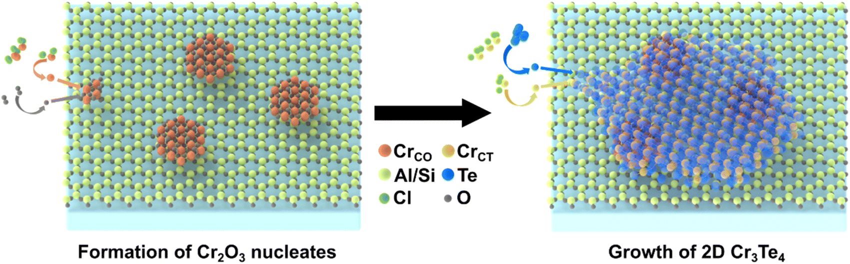 | ||
| Fig. 4 A schematic diagram illustrating the proposed crystal growth model for epitaxially grown 2D Cr3Te4 on the mica substrate. The process has two steps, with the first step being the formation of Cr2O3 seed particles, and the second step being the growth of Cr3Te4 based on Cr2O3/Cr3Te4 interfaces. | ||
Conclusions
Through combining electron diffractions and aberration-corrected STEM imaging, we found that the interface between epitaxially grown chromium chalcogenides on mica can be more complex than expected. The lack of previous study on high-resolution images at the mica-sample interface is likely due to the electron-beam sensitivity of the mica substrate, which was overcome by the low-dose imaging techniques in our work.34 Our experimental findings show that there is an oxide-assisted growth mechanism, where Cr2O3 seed nanoparticles were formed between mica and Cr3Te4. We propose that the seed nanoparticles may not just act as a Cr source during growth, but can also act as a buffer layer to release the strain at the Cr3Te4–mica interface. This growth mechanism we found provides guidance for designing epitaxial-growth procedures to obtain high-quality 2D chromium–telluride crystals.Conflicts of interest
There are no conflicts to declare.Acknowledgements
This work is supported by the National Natural Science Foundation of China (Grant No. 12104517), the Science and Technology Projects in Guangzhou, Guangzhou Basic and Applied Basic Research Foundation (202201011074), the Fundamental Research Funds for the Central Universities, Sun Yat-sen University (22qntd0101) and the Sun Yat-sen University (starting grant 29000-18841290, 29000-12220013).References
- C. Tan, J. Chen, X.-J. Wu and H. Zhang, Nat. Rev. Mater., 2018, 3, 17089 CrossRef CAS.
- M. Gibertini, M. Koperski, A. F. Morpurgo and K. S. Novoselov, Nat. Nanotechnol., 2019, 14, 408–419 CrossRef CAS PubMed.
- X. Jiang, Q. Liu, J. Xing, N. Liu, Y. Guo, Z. Liu and J. Zhao, Appl. Phys. Rev., 2021, 8, 031305 CAS.
- M. Och, M.-B. Martin, B. Dlubak, P. Seneor and C. Mattevi, Nanoscale, 2021, 13, 2157–2180 RSC.
- S. Zhang, H. Wu, L. Yang, G. Zhang, Y. Xie, L. Zhang, W. Zhang and H. Chang, Mater. Horiz., 2022, 9, 559–576 RSC.
- N. D. Mermin and H. Wagner, Phys. Rev. Lett., 1966, 17, 1133–1136 CrossRef CAS.
- C. Gong, L. Li, Z. Li, H. Ji, A. Stern, Y. Xia, T. Cao, W. Bao, C. Wang, Y. Wang, Z. Q. Qiu, R. J. Cava, S. G. Louie, J. Xia and X. Zhang, Nature, 2017, 546, 265–269 CrossRef CAS PubMed.
- B. Huang, G. Clark, E. Navarro-Moratalla, D. R. Klein, R. Cheng, K. L. Seyler, D. Zhong, E. Schmidgall, M. A. McGuire, D. H. Cobden, W. Yao, D. Xiao, P. Jarillo-Herrero and X. Xu, Nature, 2017, 546, 270–273 CrossRef CAS PubMed.
- S. Jiang, L. Li, Z. Wang, K. F. Mak and J. Shan, Nat. Nanotechnol., 2018, 13, 549–553 CrossRef CAS PubMed.
- B. Huang, M. A. McGuire, A. F. May, D. Xiao, P. Jarillo-Herrero and X. Xu, Nat. Mater., 2020, 19, 1276–1289 CrossRef CAS PubMed.
- K. S. Burch, D. Mandrus and J.-G. Park, Nature, 2018, 563, 47–52 CrossRef CAS PubMed.
- S. Lu, Q. Zhou, Y. Guo, Y. Zhang, Y. Wu and J. Wang, Adv. Mater., 2020, 32, 2002658 CrossRef CAS PubMed.
- A. Purbawati, J. Coraux, J. Vogel, A. Hadj-Azzem, N. Wu, N. Bendiab, D. Jegouso, J. Renard, L. Marty, V. Bouchiat, A. Sulpice, L. Aballe, M. Foerster, F. Genuzio, A. Locatelli, T. O. Menteş, Z. V. Han, X. Sun, M. Núñez-Regueiro and N. Rougemaille, ACS Appl. Mater. Interfaces, 2020, 12, 30702–30710 CrossRef CAS PubMed.
- R. Chua, J. Zhou, X. Yu, W. Yu, J. Gou, R. Zhu, L. Zhang, M. Liu, M. B. H. Breese, W. Chen, K. P. Loh, Y. P. Feng, M. Yang, Y. L. Huang and A. T. S. Wee, Adv. Mater., 2021, 33, 2103360 CrossRef CAS PubMed.
- M. Huang, L. Gao, Y. Zhang, X. Lei, G. Hu, J. Xiang, H. Zeng, X. Fu, Z. Zhang, G. Chai, Y. Peng, Y. Lu, H. Du, G. Chen, J. Zang and B. Xiang, Nano Lett., 2021, 21, 4280–4286 CrossRef CAS PubMed.
- X. Sun, W. Li, X. Wang, Q. Sui, T. Zhang, Z. Wang, L. Liu, D. Li, S. Feng, S. Zhong, H. Wang, V. Bouchiat, M. Nunez Regueiro, N. Rougemaille, J. Coraux, A. Purbawati, A. Hadj-Azzem, Z. Wang, B. Dong, X. Wu, T. Yang, G. Yu, B. Wang, Z. Han, X. Han and Z. Zhang, Nano Res., 2020, 13, 3358–3363 CrossRef CAS.
- X. Zhang, B. Wang, Y. Guo, Y. Zhang, Y. Chen and J. Wang, Nanoscale Horiz., 2019, 4, 859–866 RSC.
- X. Zhang, Q. Lu, W. Liu, W. Niu, J. Sun, J. Cook, M. Vaninger, P. F. Miceli, D. J. Singh, S.-W. Lian, T.-R. Chang, X. He, J. Du, L. He, R. Zhang, G. Bian and Y. Xu, Nat. Commun., 2021, 12, 2492 CrossRef CAS PubMed.
- B. Li, X. Deng, W. Shu, X. Cheng, Q. Qian, Z. Wan, B. Zhao, X. Shen, R. Wu, S. Shi, H. Zhang, Z. Zhang, X. Yang, J. Zhang, M. Zhong, Q. Xia, J. Li, Y. Liu, L. Liao, Y. Ye, L. Dai, Y. Peng, B. Li and X. Duan, Mater. Today, 2022, 57, 66–74 CrossRef CAS.
- Y. Liu and C. Petrovic, Phys. Rev. B, 2018, 98, 195122 CrossRef CAS.
- B. Tang, X. Wang, M. Han, X. Xu, Z. Zhang, C. Zhu, X. Cao, Y. Yang, Q. Fu, J. Yang, X. Li, W. Gao, J. Zhou, J. Lin and Z. Liu, Nat. Electron., 2022, 5, 224–232 CrossRef CAS.
- F. Wang, J. Du, F. Sun, R. F. Sabirianov, N. Al-Aqtash, D. Sengupta, H. Zeng and X. Xu, Nanoscale, 2018, 10, 11028–11033 RSC.
- X.-H. Luo, W.-J. Ren and Z.-D. Zhang, J. Magn. Magn. Mater., 2018, 445, 37–43 CrossRef CAS.
- Y. Fujisawa, M. Pardo-Almanza, J. Garland, K. Yamagami, X. Zhu, X. Chen, K. Araki, T. Takeda, M. Kobayashi, Y. Takeda, C. H. Hsu, F. C. Chuang, R. Laskowski, K. H. Khoo, A. Soumyanarayanan and Y. Okada, Phys. Rev. Mater., 2020, 4, 114001 CrossRef CAS.
- Z. Zhou, Y. He and Q. Wang, Phys. B, 2022, 626, 413579 CrossRef CAS.
- C. Chen, X. Chen, C. Wu, X. Wang, Y. Ping, X. Wei, X. Zhou, J. Lu, L. Zhu, J. Zhou, T. Zhai, J. Han and H. Xu, Adv. Mater., 2022, 34, 2107512 CrossRef CAS PubMed.
- M. Wang, L. Kang, J. Su, L. Zhang, H. Dai, H. Cheng, X. Han, T. Zhai, Z. Liu and J. Han, Nanoscale, 2020, 12, 16427–16432 RSC.
- Y. Guo, L. Kang, S. Yu, J. Yang, X. Qi, Z. Zhang and Z. Liu, ChemNanoMat, 2021, 7, 323–327 CrossRef CAS.
- H. Wu, W. Zhang, L. Yang, J. Wang, J. Li, L. Li, Y. Gao, L. Zhang, J. Du, H. Shu and H. Chang, Nat. Commun., 2021, 12, 5688 CrossRef CAS PubMed.
- M. Bian, A. N. Kamenskii, M. Han, W. Li, S. Wei, X. Tian, D. B. Eason, F. Sun, K. He, H. Hui, F. Yao, R. Sabirianov, J. P. Bird, C. Yang, J. Miao, J. Lin, S. A. Crooker, Y. Hou and H. Zeng, Mater. Res. Lett., 2021, 9, 205–212 CrossRef CAS.
- K. Niu, G. Qiu, C. Wang, D. Li, Y. Niu, S. Li, L. Kang, Y. Cai, M. Han and J. Lin, Adv. Funct. Mater., 2022, 2208528, DOI:10.1002/adfm.202208528.
- L. Meng, Z. Zhou, M. Xu, S. Yang, K. Si, L. Liu, X. Wang, H. Jiang, B. Li, P. Qin, P. Zhang, J. Wang, Z. Liu, P. Tang, Y. Ye, W. Zhou, L. Bao, H.-J. Gao and Y. Gong, Nat. Commun., 2021, 12, 809 CrossRef CAS PubMed.
- R. Cheng, L. Yin, Y. Wen, B. Zhai, Y. Guo, Z. Zhang, W. Liao, W. Xiong, H. Wang, S. Yuan, J. Jiang, C. Liu and J. He, Nat. Commun., 2022, 13, 5241 CrossRef CAS PubMed.
- Y.-C. Zou, L. Mogg, N. Clark, C. Bacaksiz, S. Milovanovic, V. Sreepal, G.-P. Hao, Y.-C. Wang, D. G. Hopkinson, R. Gorbachev, S. Shaw, K. S. Novoselov, R. Raveendran-Nair, F. M. Peeters, M. Lozada-Hidalgo and S. J. Haigh, Nat. Mater., 2021, 20, 1677–1682 CrossRef CAS PubMed.
- Y. Cheng, C. Zhang, Y. Xu, Z. Li, D. Chen, W. Zhu, Q. Feng, S. Xu, J. Zhang and Y. Hao, Mater. Today Commun., 2021, 29, 102766 CrossRef CAS.
- B. Zhang, J. Su, X. Guo, L. Zhou, Z. Lin, L. Feng, J. Zhang, J. Chang and Y. Hao, Adv. Sci., 2020, 7, 1903044 CrossRef CAS PubMed.
- W. Yang, S. S. Hullavarad, B. Nagaraj, I. Takeuchi, R. P. Sharma, T. Venkatesan, R. D. Vispute and H. Shen, Appl. Phys. Lett., 2003, 82, 3424–3426 CrossRef CAS.
- Y. Zhang, Y. Yao, M. G. Sendeku, L. Yin, X. Zhan, F. Wang, Z. Wang and J. He, Adv. Mater., 2019, 31, 1901694 CrossRef CAS PubMed.
- H. Li, Y. Li, A. Aljarb, Y. Shi and L.-J. Li, Chem. Rev., 2018, 118, 6134–6150 CrossRef CAS PubMed.
- J. D. Cain, F. Shi, J. Wu and V. P. Dravid, ACS Nano, 2016, 10, 5440–5445 CrossRef CAS PubMed.
- S. Saini, P. Mele, H. Honda, T. Suzuki, K. Matsumoto, K. Miyazaki, A. Ichinose, L. Molina Luna, R. Carlini and A. Tiwari, Thin Solid Films, 2016, 605, 289–294 CrossRef CAS.
- D. Zhu, H. Shu, F. Jiang, D. Lv, V. Asokan, O. Omar, J. Yuan, Z. Zhang and C. Jin, npj 2D Mater. Appl., 2017, 1, 8 CrossRef.
Footnote |
| † Electronic supplementary information (ESI) available. See DOI: https://doi.org/10.1039/d2na00835a |
| This journal is © The Royal Society of Chemistry 2023 |