
 Open Access Article
 This Open Access Article is licensed under a Creative Commons Attribution-Non Commercial 3.0 Unported Licence
Surface plasmon enhanced ultrathin Cu2ZnSnS4/crystalline-Si tandem solar cells†
Shafayeth
Jamil
 a,
Uday
Saha
b and
Md. Kawsar
Alam
*a
a,
Uday
Saha
b and
Md. Kawsar
Alam
*a
aDepartment of Electrical and Electronic Engineering, Bangladesh University of Engineering and Technology, Dhaka, 1205, Bangladesh. E-mail: kawsaralam@eee.buet.ac.bd; kawsar.alam@alumni.ubc.ca
bDepartment of Electrical and Computer Engineering and Institute of Research in Electronics and Applied Physics (IREAP), University of Maryland, College Park, Maryland 20742, USA
First published on 12th April 2023
Abstract
Thin-film silicon solar cells have sparked a great deal of research interest because of their low material usage and cost-effective processing. Despite the potential benefits, thin-film silicon solar cells have low power-conversion efficiency, which limits their commercial usage and mass production. To solve this problem, we design an ultrathin dual junction tandem solar cell with Cu2ZnSnS4 (CZTS) and crystalline silicon (c-Si) as the main absorbing layer for the top and bottom cells, respectively, through optoelectronic simulation. To enhance light absorption in thin-film crystalline silicon, we use silver nanoparticles at the rear end of the bottom cell. We utilize amorphous Si with a c-Si heterojunction to boost the carrier collection efficiency. Computational analyses show that within 9 μm thin-film c-Si, we achieve 28.28% power conversion efficiency with a 220 nm top CZTS layer. These findings will help reduce the amount of Si (∼10 vs. ∼180 μm) in silicon-based solar cells while maintaining high power conversion efficiency.
1. Introduction
The need for sustainable energy development has significantly increased interest in renewable resources. Solar energy is a prominent renewable energy source that provides “limitless” emission-free energy. Among many semiconductor materials, silicon has a nearly 70 year development history for photovoltaic purposes. Si-wafer based PV technology accounted for about 95% of the total production in 2020 (ref. 1) because of several reasons: silicon is the second most abundant element in the Earth's crust; the bandgap of silicon is within the optimal region (1.1–1.4 eV) for efficient solar energy conversion; it is stable and non-toxic and silicon semiconductor technology is well established. The current crystalline silicon (c-Si) solar cell efficiency record is 26.7%.2 However, the maximum achievable power conversion efficiency (PCE) is limited to 29.43% (ref. 3) by silicon's indirect bandgap at 1.12 eV and nonradiative auger recombination-a dominant intrinsic loss mechanism for a c-Si photovoltaic cell. Another bottleneck for c-Si solar cell development is the material cost, which represents about 50% of the cost of a solar panel.4 Due to silicon's indirect bandgap, photocurrent obtained using single-pass absorption is quite low unless the thickness surpasses many tens of microns. Thus, to achieve a sufficient photocurrent, the thickness of c-Si needs to be around 100–200 μm, while the current industry standard for wafer-based c-Si solar cells is 180 μm.5 Consequently, there is a tradeoff between higher efficiency and material cost while developing silicon photovoltaic cells.Several strategies have been used to obtain highly efficient silicon based solar cells. Although the PERC cell is the most efficient silicon homojunction solar cell,6 significant improvements have been made since 2015, owing primarily to the development of Si heterojunction (SHJ) solar cells formed between hydrogenated amorphous silicon (a-Si:H) and crystalline silicon (c-Si) absorbers using improved passivating contact technology. The present success of SHJ solar cells is primarily attributed to the fact that they combine bulk c-Si and thin film solar cell technology, integrating the advantages of both.7 SHJ cells are further improved through developing the heterojunction with intrinsic thin-layer (HIT) cells by inserting a thin intrinsic layer between a-Si and c-Si layers. As a result, the carrier collection efficiency in the device improves. This technology enabled the development of high efficiency Si solar cells with a wafer thickness below 100 μm at a low processing temperature (200 °C).8 Moreover, the Staebler–Wronski effect observed in amorphous silicon solar cells does not occur in SHJ solar cells, as the base material of the structure is crystalline silicon.9 Furthermore, compared to standard c-Si solar cells (−0.45%/K), the HIT solar cell shows a better temperature coefficient (<−0.25%/K).10 However, achieving high HIT solar cell efficiency requires a high-quality a-Si:H(i) layer and a-Si:H/c-Si interface.
One of the direct ways to surpass the Shockley–Queisser efficiency limit for silicon-based solar cells is by utilizing a multi-junction tandem cell structure, which increases the spectral efficiency of the device. C–Si has a high potential for usage in multi-junction cells because its bandgap of 1.12 eV is almost ideal for a two-terminal tandem and when paired with a top absorber with a bandgap of 1.72 eV, a maximum PCE of up to 43% is possible.11 Group III–V materials and perovskite have been studied extensively as the top absorber of Si-based tandem cells.2,12 Thin film chalcogenides (TFCs) such as CdTe, CIGSSe, and CZTSSe are promising candidates for the top absorber due to their high single-junction solar cell efficiencies, direct and tunable bandgap, competitive manufacturing costs, and superior stability.13,14 Among these materials, kesterite-based Cu2ZnSnS4 (CZTS) is gaining considerable attention because it is composed entirely of abundant, non-toxic elements and exhibits a high absorption coefficient (>104 cm−1).15,16 Moreover, its bandgap is dependent on the degree of cationic disorder, ranging from about 1.5 eV in the completely disordered state to 1.65 eV in the less disordered state.17 The theoretical maximum efficiency of a tandem cell based on a top cell with a bandgap of 1.65 eV is 35%.18 Hajijafarassar et al. investigated the monolithic integration of CZTS on a Si bottom solar cell by inserting a TiN buffer layer.14 The efficiency of the tandem cell was limited to 1.1% (with a 350 μm thick Si absorber) due to the difficulty of reproducing high-quality CZTS absorbers on non-glass substrates as well as non-ohmic blocking behaviour at the TiN interfaces. Valentini et al. achieved 3.5% efficiency (with a 250 μm thick Si absorber) using a MoS2/FTO/ZnO trilayer structure as an intermediate contact between the top and the bottom cells with poor short circuit current density (Jsc) (6 mA cm−2) because of the low transmittance of the trilayer intermediate contact.19 Overall, further research is required to develop an ohmic intermediate layer with high transmittance. Additionally, it is necessary to increase the short circuit current of the tandem cell, which can be achieved by enhancing the photon absorption of the tandem cell. At the same time, it is important to reduce the thickness of the Si absorber layer in order to build ultrathin, high-performance Si solar cells that could reduce the cost of commercial silicon based photovoltaics.
Typically, single-pass light absorption within the absorber layers of any thin-film solar cell is relatively low. Thus, several light absorption enhancement techniques based on increasing the optical path length and embedding scatterers within cells have been developed to increase efficiency. Plasmonic light trapping is a popular approach for effective light coupling into the cell while avoiding the adverse effects of surface texturing, such as increased surface recombination. As a result, the solar cell's absorption improves, leading to a rise in short circuit current and conversion efficiency. Plasmonic nanostructures have been employed in at least three different configurations:20 on the cell's surface,21,22 embedded in the active layer,23,24 and at the bottom interface between the semiconductor and metal in the form of metal nanoparticles (MNPs)25–27 or surface plasmonic gratings.28 Zhang et al. theoretically studied nanoparticle integrated ultra-thin solar cells with a Si thickness of 20 μm that can potentially achieve 18.2% efficiency by combining the absorption enhancement with the benefit of a thinner Si induced open circuit voltage increase.29 Yan et al. achieved 15.1% efficient ultrathin (20 μm) front-textured crystalline silicon solar cells with rear-located periodic silver nanoarrays.30 Marom et al. observed a clear optical absorption increase in the a-Si thin films in the NIR by integrating silver nanoparticles.31 The performance of these plasmonic solar cells can be further enhanced by employing a tandem cell structure, since adding another absorber would enhance the total light absorption of the device.
All the techniques mentioned above improve the performance of Si solar cells, which motivated us to combine plasmonics, HIT cell and tandem cell technologies to develop a highly efficient thin film CZTS/Si tandem cell. In this paper, we have designed and investigated the prospects of ultrathin CZTS/Si heterojunction tandem solar cells with an integrated plasmonic back reflector through computational analysis. We have also studied the effect of metal nanoparticles in the tandem solar cell as well as optimized the absorbers' thicknesses to maximize the performance of the tandem cell.
2. Device modeling and simulation method
Fig. 1 illustrates the architecture of a CZTS/Si tandem solar cell. The top cell architecture (ZnO/CdS(n)/CZTS(p)) is modeled based on an experimental structure proposed by Shin et al.32 Here, CZTS and CdS work as the primary absorber layer and buffer layer, respectively. An N-type transparent ZnO window layer acts as the top surface field layer. CdS and ZnO are both 30 nm thick. The thickness of the CZTS layer has been varied later for the current matching purpose. 50 nm MgF2 is applied on top of ZnO as an antireflection coating layer. The HIT structure is used in the bottom cell design with Ag nanoparticles incorporated in the MgF2/Ag back reflector at the rear of the structure for plasmonic enhancement. In the design, n-type c-Si works as the main bottom cell absorber. 5 nm intrinsic a-Si:H passivation layers are placed on both sides of the c-Si. N-doped a-Si:H and p-doped a-Si:H act as emitter and back surface field layers, respectively. The thickness of both n-doped and p-doped a-Si:H layers is 10 nm. In the backside of the cell, we placed an array of hemispherical silver (Ag) MNPs embedded in a 100 nm thick MgF2 layer, followed by a rear Ag mirror, similar to configurations that have shown EQE enhancement.25 Hemispherical nanoparticles are used to improve the coupling of scattered light into the Si layer. It was observed that the maximum plasmonic coupling is achieved if the pitch of the Ag MNPs is ∼750–900 nm (ESI, section S4†). Therefore, we considered the array period of Ag MNPs to be 750 nm for the rest of the simulation. Between the a-Si:H(p) layer and the Ag nanoparticles, a 20 nm SiO2 spacer layer is inserted, which is necessary for enhanced light trapping and high-quality surface passivation.25 Small contact windows are opened on the rear SiO2 layer through which a-Si (p) is connected to the back contact. No transparent conductive oxide (TCO) layer is used in the back contact, as high-efficiency SHJ without TCO in rear a-Si:H(p)/Ag emitter contact has been demonstrated, which was achieved by proper junction engineering.33 To connect the bottom and top cells, a 30 nm ITO recombination layer is inserted between the two cells. Along with the other parts of the tandem solar cell, the CZTS/ITO interface is experimentally realizable.34 Therefore, the proposed structure can be realized using currently available fabrication technology.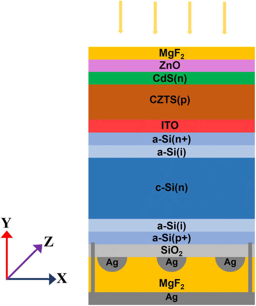 | ||
| Fig. 1 Cross-sectional schematic of the Cu2ZnSnS4 (CZTS)/Si tandem cell with a plasmonic back reflector. The CZTS top cell and si bottom cell are connected by an ito recombination layer. The hemispherical plasmonic Ag nanoparticles (NPs) are embedded in a 100 nm MgF2 dielectric layer followed by an Ag mirror which also serves as the back contact. Between the bottom cell and the Ag NPs, a 20 nm SiO2 spacer layer is inserted for passivation purposes. | ||
Next, we studied the junction energy levels to assess the carrier collection efficiency of the tandem cell.35Fig. 2 illustrates the energy band diagram of the tandem cell. In this case, a spike-like conduction band offset (CBO) is observed at the CdS/CZTS interface, which is supported by high-performance devices.32,36 However, the band alignment of CdS/CZTS in lower performance devices has been reported to be cliff-type which limits the Voc of solar cells by assisting interfacial recombination.37 The interfacial defects at the CdS/CZTS junction can be reduced by epitaxial growth of CBD-CdS and Cd diffusion.38 The holes produced at the CZTS absorber do not reach the cathode side due to the energy barrier created by CdS and the ZnO layer. These holes reach the ITO recombination layer, recombining with the electrons generated at the c-Si absorber. The surface dangling bonds and defects in the c-Si/a-Si junction are passivated by inserting a high-quality 5 nm intrinsic a-Si layer between the two layers using a low-damage process. Again, the electrons produced at the c-Si absorber are restricted by the a-Si (p) back surface field layer; thus, these electrons cannot reach the anode. However, the holes can easily cross the narrow spike-like CBO at the c-Si/a-Si junction at the rear end of the cell to reach the anode. Overall, the cell is designed to maximize the carrier collection efficiency of the tandem cell.
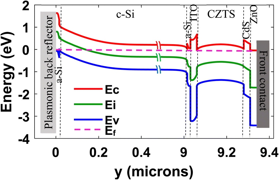 | ||
| Fig. 2 Energy band diagram of the CZTS/Si tandem cell under equilibrium conditions. | ||
We used rigorous optoelectronic simulation to evaluate the performance of our proposed tandem cell. To simulate the tandem solar cell, we used the methodology as previously utilized by our team.39 The optical40–48 and the electrical32,48–62 parameters were extracted from the literature. Additionally, we have listed the electronic properties in the ESI (section S1)†. Moreover, we benchmarked our used parameters by modeling experimental solar cells to ensure the reliability of the simulation results, which can be found in the ESI (section S2).† In this regard, first, light absorption and carrier generation rates were calculated by solving Maxwell's curl equation through finite difference time domain (FDTD) analysis. The electrical characteristics of the top CZTS cell and bottom Si cell were calculated independently by solving the Poisson equation, continuity equation, and drift-diffusion equation self-consistently. Next, we modeled the top and bottom cells separately by using equivalent circuits and then combined them using Matlab Simulink to obtain the electrical characteristics of the tandem cell. We compared the J–V characteristics obtained from the circuit model to the device simulation results for both the top and bottom cells to ascertain that the circuit model can accurately reproduce the behavior of the top and bottom cells calculated from the device simulations (ESI, section S3†). More details on theoretical model including simulation equations can be found in ref. 39.
3. Results and discussion
3.1 Effects of plasmonic nanoparticles
First, we investigated the effects of Ag nanoparticles on the performance of the CZTS/Si tandem solar cell. To start our analysis, we considered the top and bottom absorber thicknesses of 200 nm and 9 μm, respectively. As mentioned earlier, absorber thicknesses have been optimized later. Fig. 3(a) shows the absorption spectrum of the tandem cell, top cell, and bottom cell without Ag nanoparticles. Photons with a wavelength less than 600 nm are mostly absorbed in the top CZTS cell, while longer wavelength photons (>900 nm) are mainly absorbed in the bottom Si cell.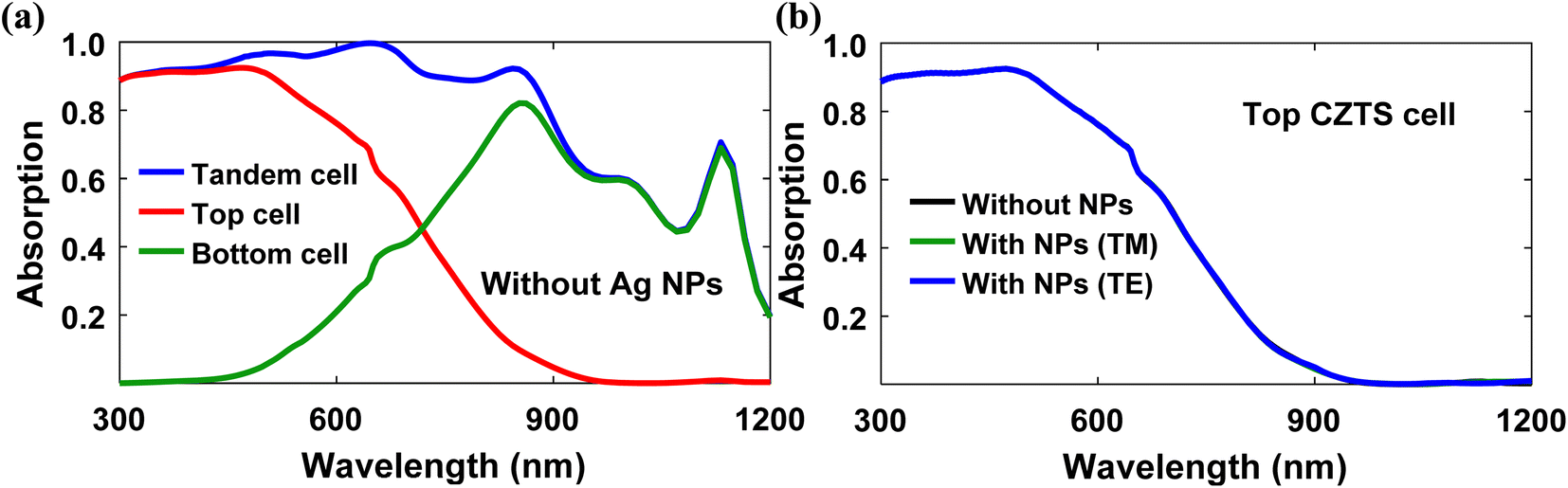 | ||
| Fig. 3 Absorption as a function of wavelength in the (a) top CZTS cell, bottom Si cell and overall tandem cell without Ag nanoparticles and (b) top CZTS cell with and without Ag NPs. The top cells with and without Ag NPs show identical absorption spectra for TM and TE polarized illumination. Therefore, Ag NPs do not improve the light absorption of the CZTS top cell. | ||
The total absorption in the tandem cell, which is the sum of top and bottom cell absorption, is relatively high (>0.8) until 900 nm, although it declines for higher wavelength photons. Thus, absorption enhancement in the tandem cell beyond 900 nm wavelength is the primary concern. To improve the total absorption of low energy photons, we integrated hemispherical Ag nanoparticles at the rear end of the tandem cell. However, it should be noted that no absorption enhancement can be observed in the top cell (Fig. 3(b)) since almost all shorter wavelength photons are absorbed by a single pass through the tandem cell and do not reach the Ag nanoparticles. As a result, surface plasmon resonance (SPR) does not exist and absorption remains the same for lower wavelength light. For this reason, we only studied the impact of Ag nanoparticles on the bottom Si cell.
Fig. 4 compares light absorption in the bare (without Ag NPs) bottom cell with that in the plasmonic bottom cell. A broadband absorption improvement is achieved for TM polarized light for wavelengths longer than 850 nm. Absorption enhancement is also found for TE polarized illumination; however, the plasmonic cell exhibits lower TE polarized light absorption in the 1100–1170 nm wavelength region than the bare solar cell.
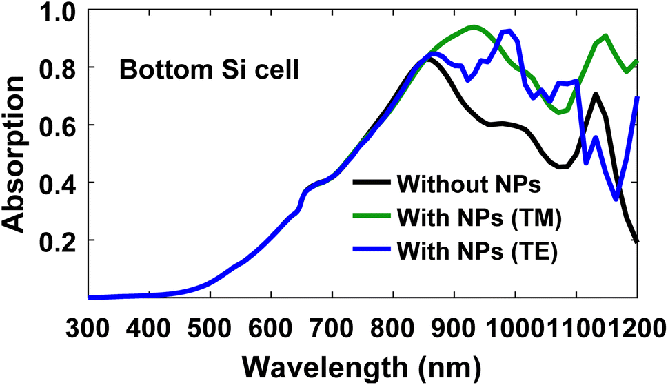 | ||
| Fig. 4 Comparison of absorption spectra between bottom Si cells with and without Ag NPs for TM and TE polarized light. Due to the incorporation of Ag NPs, the Si cell exhibits enhanced broad-band light absorption beyond 900 nm wavelength. | ||
Incident electromagnetic radiation excites localized surface plasmon (LSP) resonances on the Ag metal particles, which then scatter light back into the Si absorber at resonant wavelengths. Efficient scattering of photons into active materials increases the length of the photon path, leading to increased absorption. The amplification of the optical electric field, |![[E with combining right harpoon above (vector)]](https://www.rsc.org/images/entities/i_char_0045_20d1.gif) op|/|op_in| (expressed as the ratio of the magnitude of the optical electric field, op, to the magnitude of the incident optical electric field, op_in), within the active layer at different wavelengths due to Ag nanoparticles is illustrated in Fig. 5. For both TM (Fig. 5(a)) and TE (Fig. 5(e)) polarized light, the electric field can improve the incident field up to 2 times at 1200 nm wavelength. Moreover, it can be noted that the field enhancement declines with decreasing wavelengths. Since the electric field can increase two times the incident field, the optical electric field intensity (|op|2) may enhance up to fourfold, significantly boosting the Si absorber's absorption and improving the bottom cell's performance. Overall, Ag nanoparticles improve both photon scattering and the optical-electric field within the Si bottom cell, resulting in improved power absorption in the Si bottom cell.
op|/|op_in| (expressed as the ratio of the magnitude of the optical electric field, op, to the magnitude of the incident optical electric field, op_in), within the active layer at different wavelengths due to Ag nanoparticles is illustrated in Fig. 5. For both TM (Fig. 5(a)) and TE (Fig. 5(e)) polarized light, the electric field can improve the incident field up to 2 times at 1200 nm wavelength. Moreover, it can be noted that the field enhancement declines with decreasing wavelengths. Since the electric field can increase two times the incident field, the optical electric field intensity (|op|2) may enhance up to fourfold, significantly boosting the Si absorber's absorption and improving the bottom cell's performance. Overall, Ag nanoparticles improve both photon scattering and the optical-electric field within the Si bottom cell, resulting in improved power absorption in the Si bottom cell.
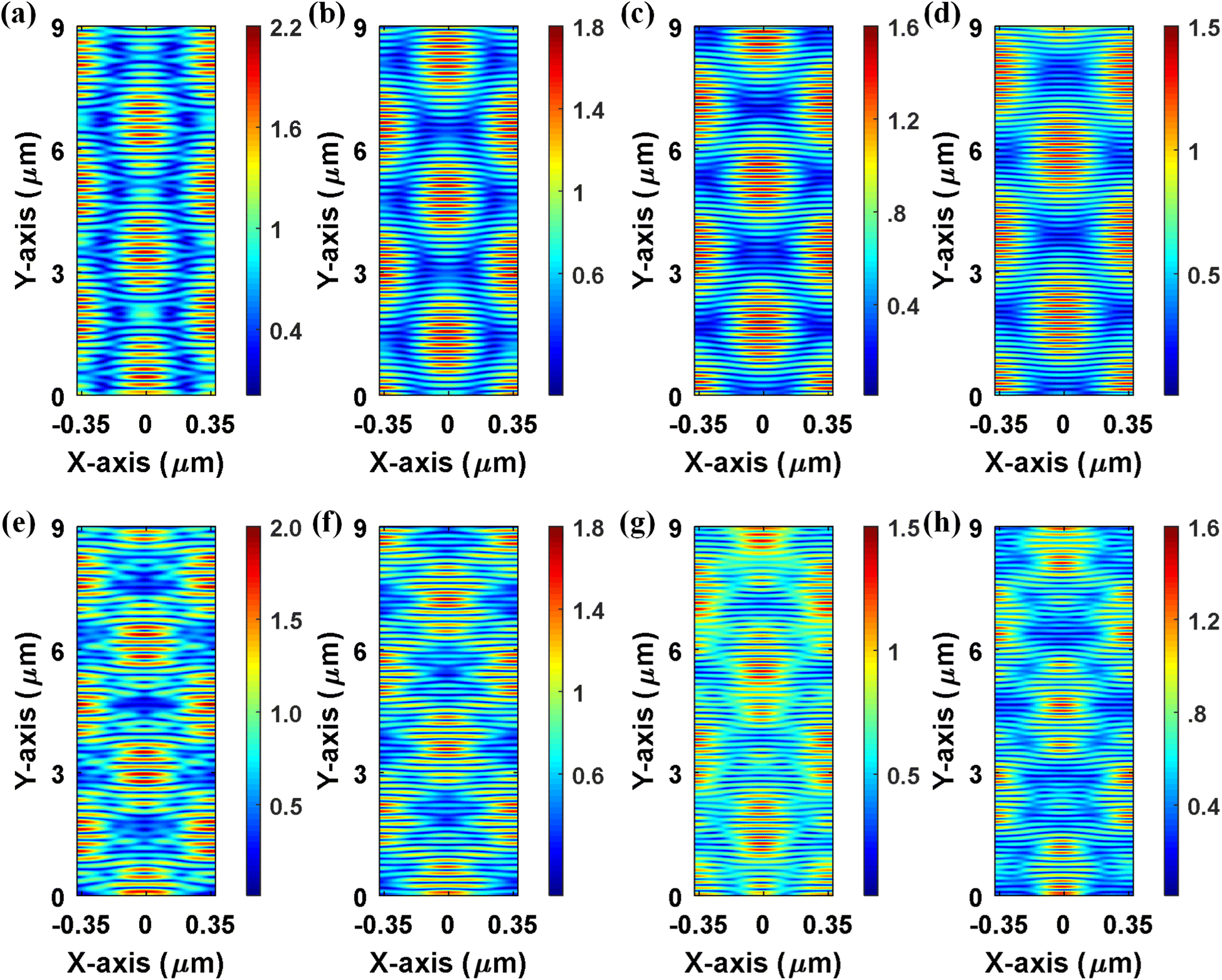 | ||
| Fig. 5 Electric-field enhancement in the bottom Si cell for TM polarized light at wavelengths (a) 1200 nm, (b) 1100 nm, (c) 1050 nm, and (d) 980 nm, and for TE polarized light at wavelengths (e) 1200 nm, (f) 1085 nm, (g) 1000 nm and (h) 965 nm. | ||
Fig. 6 compares the overall absorption in the plasmonic Si bottom cell (the average of TM and TE polarized light absorption) and the bare bottom cell. Improved absorption for longer wavelength light (>900 nm) is attained, which was the primary motivation for introducing Ag nanoparticles, as discussed previously. Absorption enhancement is ∼150% for the 900–1100 nm wavelength range, which reaches up to 400% for 1200 nm wavelength. Moreover, the reduced absorption enhancement in the 1100–1150 nm range is not a major issue because the AM 1.5G solar spectrum exhibits relatively lower spectral irradiance in this range. Thus, higher absorption enhancement in this range would have had little effect on the cell's performance.
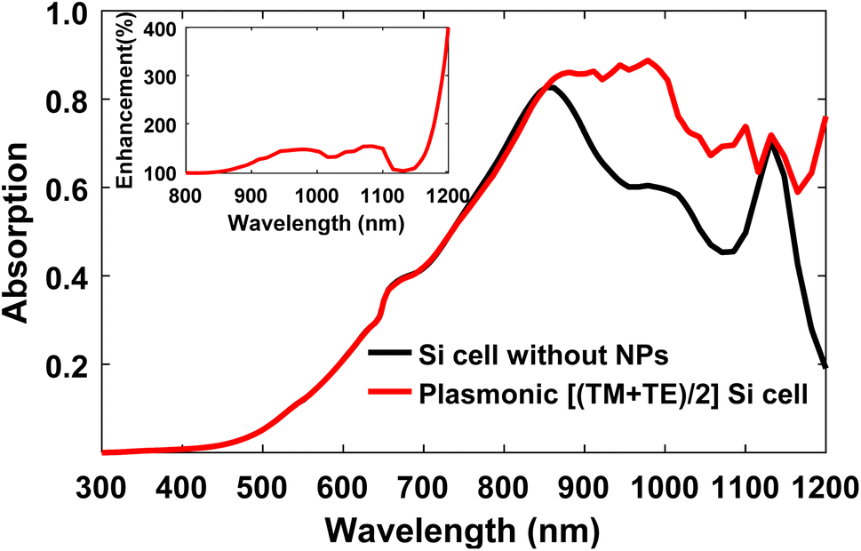 | ||
| Fig. 6 Comparison of overall absorption spectra (the average of TM and TE polarized light absorption) in bottom Si cells without and without Ag NPs. The inset shows the absorption enhancement in the bottom cell due to the insertion of Ag nanoparticles. | ||
Next, we investigated the effect of the size of the hemispherical Ag nanoparticles on the performance of the Si bottom cell. The absorbed power (Pabs) enhancement due to the insertion of Ag nanoparticles was calculated using the following formula:
 | (1) |
Fig. 7(a) illustrates Pabs enhancement as a function of the radius of hemispherical Ag nanoparticles. The enhancement is minimal for smaller particles (<100 nm), as the enhancement provided by small particles is limited by plasma damping due to surface scattering.63 Furthermore, the plasmon resonance range is narrow for smaller particles (Fig. 7(b)); thus, broadband enhancement is not achieved. On the other hand, power absorption improves with increasing nanoparticle size, as scattering is more efficient than absorption for larger particles.64 Moreover, from Fig. 7(b), it can be observed that the resonance peak red-shifts with an increasing nanoparticle radius, which happens due to dynamic depolarization in larger plasmonic metal nanoparticles.65 Additionally, absorption spectra become broader as a result of radiation damping.63,65
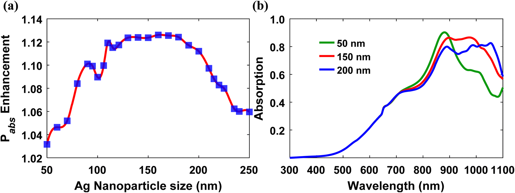 | ||
| Fig. 7 (a) Power absorption (Pabs) enhancement in a plasmonic Si bottom cell as a function of Ag nanoparticles' radius, and (b) optical absorption spectra of a plasmonic bottom cell incorporating different Ag nanoparticles. | ||
The red-shift and broadening of the resonance with increased particle size cause significant Pabs enhancement. The Pabs enhancement is maximum (>1.12) for the 130–180 nm radius range. Beyond a radius of 180 nm, Pabs enhancement decreases with the magnitude of the plasmonic resonance, and absorption declines due to radiation damping.63,65 As a result, relatively large particles lose their plasmonic characteristics.
Considering that the maximum enhancement in power absorption occurs for nanoparticles with a radius of 130–180 nm, we used 130 nm Ag nanoparticles for the rest of the analysis.
3.2 Thickness optimization of the tandem cell
The current mismatch between cells is one of the major issues reducing a tandem device's final output efficiency. For this reason, we optimized the thickness of CZTS and Si absorbers to improve the performance of the tandem solar cell through current matching. In this regard, optical interference with thickness needs to be discussed since optical interference might be used for an additional light trapping mechanism.66Fig. 8 shows the absorption spectrum for different c-Si layer thicknesses. It can be observed that there are various wavelengths with greater absorption, indicating constructive interference in these wavelengths. As reflection at the a-Si/c-Si interfaces is negligible due to the extremely thin a-Si layer thickness and the roughly similar refractive indices of a-Si and c-Si, these interference patterns are primarily produced at the SiO2/Ag back reflector interface. It can be observed that with increasing thickness of the absorber layer, the number of wavelengths at which constructive interference occurs also increases. However, this is not the primary reason for photocurrent enhancement with increasing thickness. The absorption spectrum also moves upwards with increasing thickness indicating the absorption length enhancement in the absorber, facilitating greater light absorption. The bottom cell's photocurrent increases with absorber thickness mainly for this reason.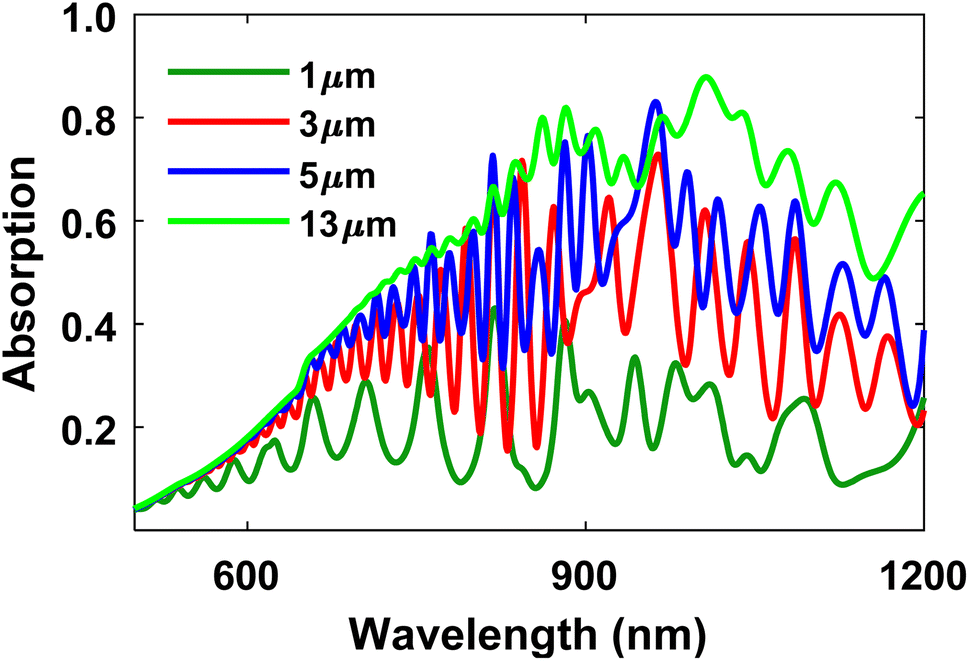 | ||
| Fig. 8 Absorption in the c-Si absorber at different thicknesses indicating the interference pattern at different wavelengths. | ||
Fig. 9(a) illustrates the dependence of a tandem cell's Jsc on the CZTS and Si absorber's thicknesses. CZTS absorbs a significant amount of radiation at a relatively lower thickness (170 to 230 nm) since, in a tandem structure, the top cell absorbs high-energy photons with relatively short absorption depth. Further increasing the thickness of CZTS results in lower Jsc in the top cell due to increased carrier recombination. Additionally, a thicker top absorber allows very little optical radiation to reach the bottom cell, resulting in a larger current mismatch. On the other hand, the Si bottom cell shows a high current density at a very thin thickness (∼9 μm) due to the introduction of plasmonic nanoparticles in the bottom cell, which significantly improves the absorbance of the cell at longer wavelengths. Furthermore, recombination loss in the ultrathin Si absorber is reduced considerably, boosting the short circuit current through improved carrier collection. At 210 nm CZTS and 9 μm Si, the maximum Jsc of 20.21 mA cm−2 was achieved. Since we observe high Jsc at a wide range of CZTS and Si thicknesses, we analyzed the effect of absorbers thicknesses on the tandem cell's open circuit voltage, Voc.
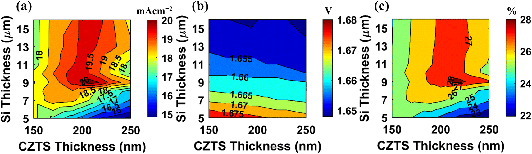 | ||
| Fig. 9 Variation of (a) short circuit current density (Jsc), (b) open circuit voltage, (Voc) and (c) efficiency of the plasmonic CZTS/Si tandem cell with the thicknesses of CZTS and c-Si absorbers. | ||
In contrast to the open circuit current of a tandem cell, which is equal to the minimum Jsc of the two cells, the open circuit voltage of a tandem cell is roughly equal to the sum of the individual Voc of top and bottom cells. As a result, in order to optimize the Voc of the tandem cell, the open circuit voltages of the individual cells must be maximized. Fig. 9(b) shows that Voc is maximum when the thickness of both cells is small. With increasing thickness, the bulk recombination in absorbers increases, which reduces the Voc in the top and bottom cells. The highest Voc (1.68 V) is obtained at 150 nm of CZTS and 5 μm of Si. Further decreasing the thicknesses of the absorbers would have reduced the open circuit voltage because of the reduction of electron–hole pair generation in ultrathin absorbers. The fill factor of the tandem cell is between 83 and 89%.
Finally, we analyzed the variation of tandem efficiency with top and bottom cells' absorber thicknesses (Fig. 9(c)). The maximum efficiency of 28.28% can be obtained at 220 nm CZTS and 9 μm Si. Moreover, we compared the plasmonic tandem cell with the back textured tandem cell (ESI, section S5†). The textured cell results in poorer optical power absorption in the 700–1000 nm wavelength range compared to the plasmonic tandem cell. As a result, the total efficiency of the back textured cell is ∼8% lower than that of the plasmonic cell (28.28 vs. 26.24%).
Fig. 10(a) illustrates the J–V and P–V characteristics of the fully optimized plasmonic CZTS/Si tandem cell. The comparison of performance characteristics between tandem cells with and without a plasmonic back reflector is given in Table 1. Because of the light trapping mechanism, the plasmonic cell shows a Jsc of 19.93 mA cm−2 which is ∼39.76% higher than that of the tandem cell without the plasmonic back reflector. Thus, the usage of a plasmonic back reflector significantly improves the short circuit current of the tandem cell. Since the open circuit voltage is logarithmically dependent on the photocurrent, only a slight increase in Voc (1.654 V to 1.662 V) is achieved. The overall PCE is improved by ∼34.66% (from ∼21% to 28.28). In this regard, the highest experimentally reported efficiency of a CZTS solar cell is 11%67 which was improved theoretically to 19.4% by direct integration of a thin Si layer with a thickness as low as 2 μm between the Mo back-contact and the primary CZTS active layer.68 Our tandem cell without a plasmonic back reflector achieves ∼8.24% efficiency improvement (∼21 vs. 19.4%) over the double-absorber hybrid model. This improvement can be attributed to tandem structure implementation, increasing Si absorber thicknesses to 9 μm and using an antireflection coating layer. Fig. 10(b) illustrates the power absorption spectrum of the fully optimized plasmonic CZTS/Si tandem solar cell.
 | ||
| Fig. 10 (a) Current–voltage (J–V) and power–voltage (P–V) characteristics and the (b) power absorption spectrum of the fully optimized plasmonic CZTS/Si tandem solar cell. The thickness of the top cell CZTS absorber is 220 nm and the bottom cell c-Si absorber is 9 μm. The radius of the hemispherical ag nanoparticles is 130–180 nm. | ||
| Tandem cell | V oc (V) | J sc (mA cm−2) | FF (%) | Efficiency (%) |
|---|---|---|---|---|
| Without a plasmonic back reflector | 1.654 | 14.26 | 89 | 20.99 |
| With a plasmonic back reflector | 1.662 | 19.93 | 85.38 | 28.28 |
The performances of several Si-based solar cells are listed in Table 2. The plasmonic CZTS/Si tandem cell provides superior performance compared to the III–V/Si tandem cells and is only surpassed by the Perovskite/Si tandem cell. In addition, the proposed plasmonic tandem cell's performance is much superior to existing ultrathin silicon photovoltaics.
| Cell type | Si absorber thickness (μm) | V oc (V) | J sc (mA cm−2) | FF (%) | Efficiency (%) |
|---|---|---|---|---|---|
| This work | 9 | 1.662 | 19.93 | 85.38 | 28.28 |
| Ultrathin c-Si69 | 10 | 0.589 | 33.9 | 78.5 | 15.7 |
| Ultrathin c-Si70 | 10 | 0.623 | 29 | 76 | 13.7 |
| Single junction c-Si2 | 165 | 0.738 | 42.65 | 84.90 | 26.7 |
| Perovskite/Si tandem71 | 260 | 1.90 | 19.26 | 79.52 | 29.15 |
| AlGaAs/Si tandem12 | 300 | 1.55 | 27.90 | 58 | 25.20 |
3.3 Impact of the dielectric medium
In addition, we investigated the effects of the dielectric medium surrounding the Ag nanoparticles to find out the best dielectric material for the tandem cell. The dependence of photocurrent (Jph) of the bottom Si cell as a function of the refractive index of the insulator medium is depicted in Fig. 11. The Jph is the maximum in three distinct refractive index regions. Compared to the other regions, region 1 (1.28–1.45) generated the maximum Jph. The refractive index of MgF2 for visible light lies within this range which is used in the proposed structure.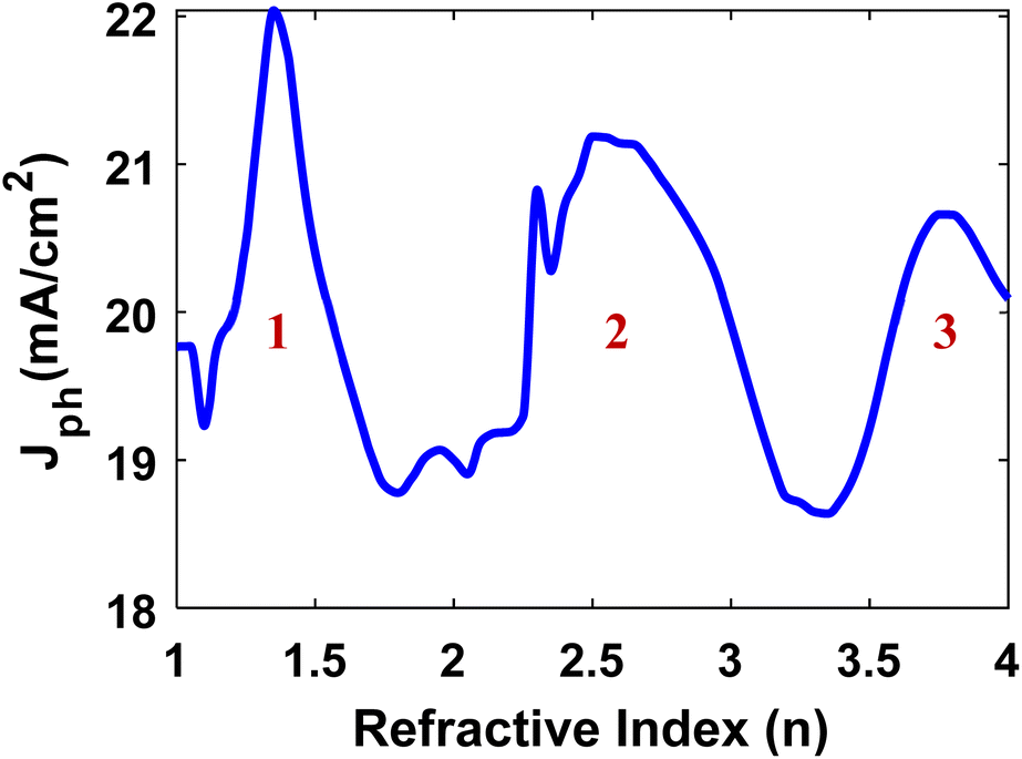 | ||
| Fig. 11 Photocurrent in the bottom cell as a function of refractive index, n of the dielectric Ag NPs embedding medium. | ||
Consequently, our structure already employs the optimal refractive index. Other fluorides such as LiF and AlF3,72 as well as oxides SiO2 and ZnO:Al have a similar refractive index. Region 2 covers the refractive index range from 2.4 to 2.8. TiO2 has a refractive index that falls into this range.73 Si has a refractive index in region 3 (3.7–3.9) for visible radiation. However, embedding nanoparticles directly in the Si absorber layer leads to significant optical and electrical losses.74
4. Conclusion
We have investigated the prospects of CZTS/Si tandem cells with plasmonic Ag nanoparticles embedded in MgF2 dielectric at the rear end of the cell. Although the characteristics of the CZTS top cell are not much altered, a significant improvement of the Si bottom cell can be observed due to the addition of Ag nanoparticles. The scattering of light into the c-Si absorber and electric field intensity is improved, resulting in higher absorbance of longer wavelength photons in the tandem cell. Absorption improvement resulted in a higher photogenerated current in the bottom cell. Furthermore, we optimized the size of the nanoparticles for the highest absorption enhancement, which was calculated to be in the 130 and 180 nm range. The thicknesses of the absorbers were also tuned for current matching of the top and bottom cells. The optimized cell consists of a 220 nm CZTS top absorber and a 9 μm bottom c-Si bottom absorber. Thus, the thickness of the c-Si absorber is significantly reduced (only ∼5% of commercial Si cells) because of the plasmonic light trapping mechanism, which would considerably reduce the tandem cell's production cost. The fully optimized solar cell achieves a PCE of 28.28%. As a result, it is feasible to manufacture silicon-based solar cells with lower material consumption and production costs that are extremely efficient.Conflicts of interest
There are no conflicts of interest to declare.References
- Fraunhofer Institute for Solar Energy Systems, Photovoltaics Report, Freiburg, 2022, https://www.ise.fraunhofer.de/content/dam/ise/de/documents/publications/studies/Photovoltaics-Report.pdf.
- M. A. Green, E. D. Dunlop, J. Hohl-Ebinger, M. Yoshita, N. Kopidakis and X. Hao, Prog. Photovoltaics Res. Appl., 2021, 29, 657–667 CrossRef.
- A. Richter, M. Hermle and S. W. Glunz, IEEE J. Photovoltaics, 2013, 3, 1184–1191 Search PubMed.
- A. Goetzberger, C. Hebling and H.-W. Schock, Mater. Sci. Eng. R, 2003, 40, 1–46 CrossRef.
- L. C. Andreani, A. Bozzola, P. Kowalczewski, M. Liscidini and L. Redorici, Adv. Phys.: X, 2019, 4, 1548305 CAS.
- M. A. Green, Adv. Mater., 2001, 13, 1019–1022 CrossRef CAS.
- K. Masuko, M. Shigematsu, T. Hashiguchi, D. Fujishima, M. Kai, N. Yoshimura, T. Yamaguchi, Y. Ichihashi, T. Mishima, N. Matsubara, T. Yamanishi, T. Takahama, M. Taguchi, E. Maruyama and S. Okamoto, IEEE J. Photovoltaics, 2014, 4, 1433–1435 Search PubMed.
- M. Taguchi, A. Yano, S. Tohoda, Y. Nakamura, K. Matsuyama, T. Nishiwaki, K. Fujita and E. Maruyama, IEEE J. Photovoltaics, 2014, 4, 96–99 Search PubMed.
- T. Sawada, N. Terada, S. Tsuge, T. Baba, T. Takahama, K. Wakisaka, S. Tsuda and S. Nakano, Proceedings of 1994 IEEE 1st World Conference on Photovoltaic Energy Conversion, 1994, vol. 2, pp. 1219–1226 Search PubMed.
- S. DeWolf, A. Descoeudres, Z. C. Holman and C. Ballif, Green, 2012, 2, 7–24 CrossRef CAS.
- Z. Yu, M. Leilaeioun and Z. Holman, Nat. Energy, 2016, 1, 16137 CrossRef.
- K. Tanabe, K. Watanabe and Y. Arakawa, Sci. Rep., 2012, 2, 349 CrossRef PubMed.
- M. Kumar, A. Dubey, N. Adhikari, S. Venkatesan and Q. Qiao, Energy Environ. Sci., 2015, 8, 3134–3159 RSC.
- A. Hajijafarassar, et al. , Sol. Energy Mater. Sol. Cells, 2020, 207, 110334 CrossRef CAS.
- C. Platzer-Björkman, N. Barreau, M. Bär, L. Choubrac, L. Grenet, J. Heo, T. Kubart, A. Mittiga, Y. Sanchez, J. Scragg, S. Sinha and M. Valentini, JPhys Energy, 2019, 1, 044005 CrossRef.
- S. C. Riha, B. A. Parkinson and A. L. Prieto, J. Am. Chem. Soc., 2009, 131, 12054–12055 CrossRef CAS PubMed.
- M. Valentini, C. Malerba, F. Menchini, D. Tedeschi, A. Polimeni, M. Capizzi and A. Mittiga, Appl. Phys. Lett., 2016, 108, 211909 CrossRef.
- I. Almansouri, A. Ho-Baillie, S. P. Bremner and M. A. Green, IEEE J. Photovoltaics, 2015, 5, 968–976 Search PubMed.
- M. Valentini, C. Malerba, L. Serenelli, M. Izzi, E. Salza, M. Tucci and A. Mittiga, Sol. Energy, 2019, 190, 414–419 CrossRef CAS.
- H. A. Atwater and A. Polman, Nat. Mater., 2010, 9, 205–213 CrossRef CAS PubMed.
- D. Zhang, X. Yang, X. Hong, Y. Liu and J. Feng, Opt. Quantum Electron., 2015, 47, 1421–1427 CrossRef CAS.
- S. Pillai, K. R. Catchpole, T. Trupke and M. A. Green, J. Appl. Phys., 2007, 101, 093105 CrossRef.
- J.-Y. Lee and P. Peumans, Opt. Express, 2010, 18, 10078–10087 CrossRef CAS PubMed.
- P. Spinelli and A. Polman, Opt. Express, 2012, 20, A641–A654 CrossRef CAS PubMed.
- Y. Yang, S. Pillai, H. Mehrvarz, H. Kampwerth, A. Ho-Baillie and M. A. Green, Sol. Energy Mater. Sol. Cells, 2012, 101, 217–226 CrossRef CAS.
- H. Tan, R. Santbergen, A. H. M. Smets and M. Zeman, Nano Lett., 2012, 12, 4070–4076 CrossRef CAS PubMed.
- M. J. Mendes, S. Morawiec, F. Simone, F. Priolo and I. Crupi, Nanoscale, 2014, 6, 4796–4805 RSC.
- V. E. Ferry, L. A. Sweatlock, D. Pacifici and H. A. Atwater, Nano Lett., 2008, 8, 4391–4397 CrossRef CAS PubMed.
- Y. Zhang, N. Stokes, B. Jia, S. Fan and M. Gu, Sci. Rep., 2014, 4, 4939 CrossRef CAS PubMed.
- W. Yan, Z. Tao, M. Gu and B. S. Richards, Sol. Energy, 2017, 150, 156–160 CrossRef CAS.
- S. Marom, M. Dorresteijn, R. Modi, A. Podestà and M. Di Vece, Mater. Res. Express, 2019, 6, 045012 CrossRef.
- B. Shin, O. Gunawan, Y. Zhu, N. A. Bojarczuk, S. J. Chey and S. Guha, Prog. Photovoltaics Res. Appl., 2013, 21, 72–76 CrossRef CAS.
- M. Bivour, C. Reichel, M. Hermle and S. W. Glunz, Sol. Energy Mater. Sol. Cells, 2012, 106, 11–16 CrossRef CAS.
- J. Ge, J. Chu, J. Jiang, Y. Yan and P. Yang, ACS Appl. Mater. Interfaces, 2014, 6, 21118–21130 CrossRef CAS PubMed.
- H. Bitam, et al. , Appl. Sol. Energy, 2022, 58, 198–202 CrossRef.
- A. Crovetto, et al. , Appl. Phys. Lett., 2017, 110, 083903 CrossRef.
- M. Bär, et al. , Appl. Phys. Lett., 2011, 99, 222105 CrossRef.
- F. Liu, et al. , Adv. Energy Mater., 2016, 6, 1600706 CrossRef.
- U. Saha and M. K. Alam, RSC Adv., 2017, 7, 4806–4814 RSC.
- M. Bass, V. N. Mahajan and E. Van Stryland, Handbook of Optics, McGraw-Hill, USA, 3rd edn, 2010, vol. 2 Search PubMed.
- M. Fang, A. Aristov, K. v. Rao, A. v. Kabashin and L. Belova, RSC Adv., 2013, 3, 19501–19507 RSC.
- W. L. Bond, J. Appl. Phys., 1965, 36, 1674–1677 CrossRef CAS.
- J.-H. Lee, K.-H. Ko and B.-O. Park, J. Cryst. Growth, 2003, 247, 119–125 CrossRef CAS.
- R. E. Treharne, A. Seymour-Pierce, K. Durose, K. Hutchings, S. Roncallo and D. Lane, J. Phys.: Conf. Ser., 2011, 286, 012038 CrossRef.
- D. T. Pierce and W. E. Spicer, Phys. Rev. B, 1972, 5, 3017 CrossRef.
- E. D. Palik, Handbook of Optical Constants of Solids, Academic Press, 1991, vol. 2 Search PubMed.
- H. H. Moore, J. Phys. Chem. Ref. Data, 1982, 9, 161–290 Search PubMed.
- K. Ito, Copper Zinc Tin Sulfide-Based Thin-Film Solar Cells, Wiley, 2014 Search PubMed.
- S. Y. Kuo and M. Y. Hsieh, Nanoscale, 2014, 6, 7553–7559 RSC.
- D. P. Norton, Y. W. Heo, M. P. Ivill, K. Ip, S. J. Pearton, M. F. Chisholm and T. Steiner, Mater. Today, 2004, 7, 34–40 CrossRef CAS.
- J. P. Leitão, N. M. Santos, P. A. Fernandes, P. M. P. Salomé, A. F. da Cunha, J. C. González, G. M. Ribeiro and F. M. Matinaga, Phys. Rev. B, 2011, 84, 024120 CrossRef.
- A. Janotti and C. G. van de Walle, Rep. Prog. Phys., 2009, 72, 126501 CrossRef.
- R. Stangl, A. Froitzheim, L. Elstner, and F. W. Fuhs, Proc. 17th Eur. Photovoltaic Sol. Energy Conf. Exhib., Munich, Germany, 2001 Search PubMed.
- L. Zhao, C. L. Zhou, H. L. Li, H. W. Diao and W. J. Wang, Phys. Status Solidi A, 2008, 205, 1215–1221 CrossRef CAS.
- X. Wen, X. Zeng, W. Liao, Q. Lei and S. Yin, Sol. Energy, 2013, 96, 168–176 CrossRef CAS.
- Z. Fan and J. G. Lu, J. Nanosci. Nanotechnol., 2005, 5, 1561–1573 CrossRef CAS PubMed.
- O. Madelung, Semiconductors: Data Handbook, Springer-Verlag Berlin Heidelberg, 3rd edn, 2004 Search PubMed.
- P. T. Landsberg, Recombination in Semiconductors, Cambridge University Press, 2009 Search PubMed.
- W. Martienssen and H. Warlimont, Springer Handbook of Condensed Matter and Materials Data, Springer, 2005 Search PubMed.
- U. Saha and M. K. Alam, Phys. Status Solidi RRL, 2018, 12, 1700335 CrossRef.
- U. Saha and M. K. Alam, RSC Adv., 2018, 8, 4905–4913 RSC.
- U. Saha and M. K. Alam, Sol. Energy, 2019, 184, 664–671 CrossRef CAS.
- A. Wokaun, J. P. Gordon and P. F. Liao, Phys. Rev. Lett., 1982, 48, 957–960 CrossRef CAS.
- K. Catchpole and A. Polman, Opt. Express, 2008, 16, 21793–21800 CrossRef CAS PubMed.
- M. Meier and A. Wokaun, Opt. Lett., 1983, 8, 581–583 CrossRef CAS PubMed.
- Z. Durmaz, S. Husein and R. Saive, Opt. Express, 2021, 29, 4324 CrossRef CAS PubMed.
- C. Yan, et al. , Nat. Energy, 2018, 3, 764–772 CrossRef CAS.
- T. AlZoubi, A. Moghrabi, M. Moustafa and S. Yasin, Sol. Energy, 2021, 225, 44–52 CrossRef CAS.
- M. S. Branham, W.-C. Hsu, S. Yerci, J. Loomis, S. V. Boriskina, B. R. Hoard, S. E. Han and G. Chen, Adv. Mater., 2015, 27, 2182–2188 CrossRef CAS PubMed.
- S. Jeong, M. D. McGehee and Y. Cui, Nat. Commun., 2013, 4, 2950 CrossRef PubMed.
- A. Al-Ashouri, et al. , Science, 2020, 370, 1300–1309 CrossRef CAS PubMed.
- Y. Lee, H. Sun, M. J. Young and S. M. George, Chem. Mater., 2016, 28, 2022–2032 CrossRef CAS.
- A. Bendavid, P. J. Martin and H. Takikawa, Thin Solid Films, 2000, 360, 241–249 CrossRef CAS.
- E. Moulin, J. Sukmanowski, P. Luo, R. Carius, F. X. Royer and H. Stiebig, J. Non-Cryst. Solids, 2008, 354, 2488–2491 CrossRef CAS.
Footnote |
| † Electronic supplementary information (ESI) available. See DOI: https://doi.org/10.1039/d2na00826b |
| This journal is © The Royal Society of Chemistry 2023 |