
 Open Access Article
 This Open Access Article is licensed under a Creative Commons Attribution-Non Commercial 3.0 Unported Licence
Improving infra-red polarized imaging efficiency in a bilayer wire-grid polarizer
Jiyeon
Jeon†
a,
Byong Sun
Chun†
 a,
Youryang
Seo†
ab,
Minkyeong
Kim
ac,
Hakseong
Kim
a,
Yeongho
Kim
a,
Jong Su
Kim
b and
Sang Jun
Lee
*a
a,
Youryang
Seo†
ab,
Minkyeong
Kim
ac,
Hakseong
Kim
a,
Yeongho
Kim
a,
Jong Su
Kim
b and
Sang Jun
Lee
*a
aDivision of Interdisciplinary Materials Measurement Institute, Korea Research Institute of Standards and Science, Daejeon 34113, Republic of Korea. E-mail: sjlee@kriss.re.kr
bDepartment of Physics, Yeungnam University, Gyeongsan 38541, Republic of Korea
cDepartment of Physics, Chonnam National University, Gwangju 61186, Republic of Korea
First published on 14th December 2022
Abstract
The optical, plasmonic, and imaging performance of an infra-red polarized system exceeds that of a conventional infra-red detector due to its high resolution and precision. The wire-grid polarizer has large potential for use in an infra-red polarized imaging device owing to its large polarization efficiency. In this study, we theoretically and experimentally investigate a method to improve the polarization efficiency of a wire-grid polarizer. Here, we demonstrated a high-performance wire grid polarizer with a maximum extinction ratio (ER) of 355 using a bilayer structure and dielectric material in the mid-wavelength infra-red (MWIR) region (3000 nm–5000 nm), which is a 4 times higher ER value than that of the monolayer structure. More interestingly, we were able to improve the performance of the bilayer wire-grid polarizer by devising a method to improve the surface roughness using Ar ion milling. The ER for the after-milled sample was 1255, which was markedly larger than that of the before-milled sample. The results of transmittance measurement confirmed that the improvement in the ER was due to the Fabry–Perot (F–P) phenomenon caused by constructive or destructive interference in the bilayer wire-grid structure and the enhancement of the surface smoothness. These results will help design a polarizer structure that will maximize the polarization efficiency and realize a high-performance infrared polarized imaging system.
Introduction
Infrared polarization images are used in light detection and ranging, bio-sensing, refractive-index sensing, military, optoelectronics, etc. owing to their high resolution and precision in real time. The image of an object captured by a conventional infrared detector will have a low contrast, unless the target object's temperature is significantly different from that of its surroundings. Thus, at narrow temperature differences, the object in the image nearly blends with the background.1–4 Polarized images possess different polarization properties arising from the scattering, absorption, and reflection of light due to the structure and texture of the object's surface. These properties still can be used to discern an object from the background. Hence, it can produce a considerably clearer image than the conventional system that only detects the optical radiation from an object. The polarized image enables the detection of an object that is not identified by the background.5,6The polarizer is the most important component of a polarization imaging device; common examples include angle, liquid-crystal, and wire-grid polarizers.7–10 The wire-grid polarizer is composed of an array of metal grids with a shorter period than the incident wavelength. It has garnered more interest than the other polarizers owing to its excellent polarization efficiency, wide viewing angle and wavelength range, high stability, and compatibility with other optical components.11 When an incident light wave is polarized perpendicular to the wire grid, a high-efficiency transmitted transverse magnetic (TM) wave is generated. When it is polarized parallel to the wire grid, a reflected or absorbed transverse electric (TE) wave is generated. Therefore, to improve the performance of this polarizer, the extinction ratio (ER), defined as the transmission ratio of the TM-polarized light to the TE-polarized light (ER = TTM/TTE), should be increased. The performance of a wire-grid polarizer is governed by structural parameters such as the period of the wire grid, width of the wire, depth of the grid, metal thickness, and complex refractive index of the metal. The polarizer must have a narrow and uniform pitch to achieve a high ER.11–13 Recently, Au has been widely used as a wire-grid material because it has a lower resistivity (2.44 × 10⁻⁸ Ω m) than other materials, and consequently a higher extinction coefficient in the terahertz region.13
Wire-grid polarizers of various structures with high ERs have been produced in the visible or long-wavelength infrared region. The typical structures of wire-grid polarizers are the monolayer and bilayer structures. The monolayer structure has a disadvantage in that its ER is smaller than that of the bilayer structure. Thus, polarizers with this structure tend to perform poorly. The reason the bilayer structure has a larger ER is that the light reflected from the second grid of the bilayer is partially re-reflected at the first grid, resulting in the constructive or destructive interference of light.14,15 Although the bilayer wire-grid polarizer shows better performance than the monolayer polarizer, the fabrication of the bilayer polarizer requires precise process control, complex processes, and expensive process equipment.12,15
The objective of this research was to experimentally and theoretically optimize the bilayer wire-grid polarizer performance. In order to maximize the efficiency of the bilayer wire-grid polarizer fabrication process and increase the polarization efficiency, we introduced the dielectric material and the secondary etching method using Ar ion milling on the bilayer wire-grid polarizer. To this end, first, to maximize the TM, TE, and ER, the thickness of the dielectric material was optimized to produce a bilayer structure based on the monolayer polarizer structure. Second, by using Ar ion milling, we tried to maximize the ER by improving the surface smoothness of the bilayer wire-grid polarizer. To evaluate the performance of the after-milled bilayer wire-grid polarizer with a dielectric material, transmission spectra were measured and compared with those of the monolayer and before-milled bilayer wire-grid polarizer. By using these approach methods, the ER for the after-milled bilayer polarizer was 1255, which was markedly larger than the 90 and 460 of the monolayer and before-milled bilayer polarizer samples, respectively. These results indicate that the bilayer wire-grid polarizer sample including the dielectric material with enhanced surface smoothness will maximize the polarization efficiency and realize a high-performance infrared polarized imaging system.
Experimental
Polarizer fabrication
To compare the ER between the two structures, monolayer and bilayer polarizers were fabricated using the nanoimprint method. Fig. 1 illustrates the schematic of monolayer polarizer fabrication using nanoimprint lithography. | ||
| Fig. 1 Schematic of fabrication of monolayer polarizers using nanoimprint lithography. | ||
First, an Si master mold with a period of 400 nm and a linewidth of 200 nm was fabricated using e-beam lithography. Second, the pattern of the Si master mold was duplicated using OrmoStamp® and polyethylene terephthalate (PET) to create a PET mold. Third, a 150 nm-thick layer of PMGI-SF3, a lift-off solution, was coated on a sapphire substrate and cured at 180 °C for 5 min. Subsequently, a layer of LV400 is coated on the PMGI-SF3 layer, soft-baked at 140 °C for 1 min, and imprinted with the PET mold to engrave a pattern. Finally, the nanosized pattern engraved on the resist (PMGI-SF3 and LV400) was etched by reactive ion etching (RIE). In the case of the monolayer polarizer, after etching the resist, Au was deposited and lifted off using N-Methyl-2-pyrrolidone (NMP).
To develop the bilayer polarizer, the same impressing process was repeated on a 650 nm-thick SiO2-deposited substrate. Next, a 7 nm-thick Cr mask layer was deposited on it to etch a 350 nm-thick SiO2 layer. Finally, Au was deposited on this layer.
Simulation
The ER is expressed as ER = TTM/TTE. A higher TM transmittance and a lower TE transmittance are indispensable for a higher ER. Therefore, we simulated the structure, and accordingly fabricated a polarizer with a higher ER in the mid-infrared band of 3–5 μm. The simulations were conducted using the Computer Simulation Technology (CST) Microwave Studio packages. CST Microwave studio is a simulator based on the finite integration technique (FIT) first proposed by Weiland and analyses the electromagnetic field of 3D structures.16 FIT discretizes the integral form of Maxwell's equations. This applies to the 3D structure that creates a suitable meshing system, and subdivides it into several small cuboids, the so-called grid cells. To solve this numerically, a finite calculation domain containing the considered application problems is applied. In this way, CST calculates various electromagnetic quantities such as electric fields, magnetic fields, surface currents, power flows, current densities, surface and volumetric power loss densities, electric energy densities, and magnetic energy densities. In the simulation, a GaSb substrate with a refractive index of 3.7 and structures fabricated using the period of the wire grid from the nanoimprint process (p = 400 nm), width of the wire (w = 200 nm), and thickness of Au (thmetal = 50 nm) were applied.Results and discussion
Dielectric materials can absorb transmitted light, reduce loss, and consequently improve the performance of the polarizer.17–19 To find the optimal thickness of the dielectric material, we simulated the transmittance properties of the polarizer according to the deposited-SiO2 thickness (thSiO2) with p = 400 nm, w = 200 nm, and thmetal = 50 nm. Fig. 2 is a schematic of the monolayer structure with SiO2 used in this simulation.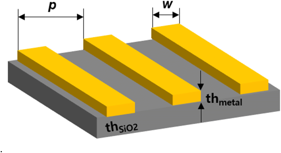 | ||
| Fig. 2 Schematic of the monolayer with SiO2 used in the simulation, where the period of the wire grid is 400 nm, the width of the wire is 200 nm, and the thickness of Au is 50 nm. | ||
Fig. 3 illustrates the TM, TE, and ER simulation results according to thSiO2. Fig. 3a depicts the change of TM according to thSiO2. Beyond a thSiO2 of 1000 nm, a resonance dip occurred as it further increased. The effect of the Fabry–Perot (F–P) resonance can also be confirmed in TE simulation. As shown in Fig. 3b, TE gradually decreases from 400 to 800 nm in thSiO2, and a small peak appeared from 1000 nm due to the F–P resonance. As illustrated in Fig. 3c, when thSiO2 is 1000 nm or greater, ER decreases in the relatively short-wavelength region due to resonance. However, when it is 600–800 nm, the TM is unaffected by resonance, and moreover no TE peak appears. Hence, the ER is large in the full-wavelength region. To realize the best possible polarizer performance with a high ER based on these results, we fabricated a bilayer polarizer with a thSiO2 of 650 nm.
 | ||
| Fig. 3 Simulation results of (a) TM, (b) TE, and (c) ER characteristics according to the thickness of the SiO2 layer. | ||
Fig. 4 shows a schematic of the monolayer structure, monolayer structure with SiO2, and bilayer structure used in this simulation. Here, the monolayer structure consists of p = 400 nm, w = 200 nm, and thmetal = 50 nm and the monolayer structure with SiO2 uses the same structure as the monolayer, whereas 650 nm of SiO2 is deposited on the substrate. The bilayer structure was fabricated by etching 350 nm of SiO2 using a photolithography process in a monolayer structure with SiO2.
 | ||
| Fig. 4 Schematic of the (a) monolayer, (b) monolayer with SiO2, and (c) bilayer structures used in the simulation, where the period of the wire grid is 400 nm, width of the wire is 200 nm, and thicknesses of Au, SiO2, and the SiO2 post layer are 50, 650, and 350 nm, respectively. | ||
Fig. 5 displays the simulation results of the transmittance characteristics according to the structure. In the wavelength range of 3–5 μm, the basic structure of the monolayer polarizer exhibited approximately a TM transmittance of 65%, and ERs of 17 and 29 at wavelengths of 3.5 and 4.5 μm, respectively.
 | ||
| Fig. 5 Simulation results of (a) TM, (b) TE, and (c) ER characteristics according to the structure. | ||
Next, a 650 nm-thick SiO2 (a monolayer with SiO2) was added to increase the TM transmitted light. The introduction of SiO2 confirmed that the TM transmittance increased above 70%, and the TE transmittance decreased. Hence, the polarizer exhibited an ER of 158 at 3.5 μm and an ER of 239 at 4.5 μm. Therefore, a dielectric material must be used to increase the ER and maximize the performance of the polarizer. However, this monolayer with the SiO2 structure exhibited non-uniform TM transmitted light in the entire wavelength region. Therefore, a bilayer structure was introduced to obtain a uniform transmittance of the TM light. According to our previous simulation results, the ER value increased as the thickness of the etched SiO2 post layer (thpost) increased. However, due to difficulties in the fabrication process with the high-aspect-ratio structure, thpost was set to 350 nm, which is smaller than p. A uniform TM transmittance of over 90% in the entire wavelength region was observed in the bilayer structure. This occurred because of the F–P phenomenon caused by constructive or destructive interference, as the light reflected from the second grid was partially re-reflected from the first grid. In the bilayer structure, the amount of light reflected by the upper and lower grids increased; therefore, the transmitted TE light significantly decreased compared with that in the monolayer. Consequently, TM transmittance increased, and TE transmittance decreased, resulting in ERs of 1.2 × 10⁴ at 3.5 μm and 1.7 × 10⁴ at 4.5 μm in the bilayer structure. Evidently, this improvement in the ER was due to the increase of the light reflectance because of the combination of the bilayer polarizer metal and the dielectric material.
To better understand the influence of the bilayer, we investigate x- and z-components of the electric field intensity along the z-direction of the structure at 3.5 μm for the three types of samples. As shown in Fig. 6 we observe the maximum accumulated charges and the x-component electric field (|Ex(Z)|y=0) around the upper metal and lower metal grating at the bilayer structure. Also, the z-component electric field (|Ez(Z)|y=0) can be considered as the coupling between the upper metal and lower metal grating, which is clearly shown in the Ez(Z) distribution. The performance of the bilayer is further enhanced by a strong coupling between the evanescent fields on the surfaces of the bilayer's metal resulting in a high TM transmission.
 | ||
| Fig. 6 Simulation results of the near-field image according to the structure. | ||
In general, light energy can cause thermal fluctuations, so this will affect the performance of the device in which the wire-grid polarizer is used.20 When the bilayer is used, the light absorption increases, so the thermal fluctuation (at this time, TM has a greater effect than TE) caused by this also acts as a very important factor in the development of a device using a wire-grid polarizer. Therefore, it is also very important to understand the thermal properties of polarized light.
To experimentally verify the performance of the polarizer as predicted through the simulation, we fabricated a polarizer with two structures on a sapphire (Al2O3) substrate. The fabricated structure was the same as the one performing optimally as predicted through the simulation.
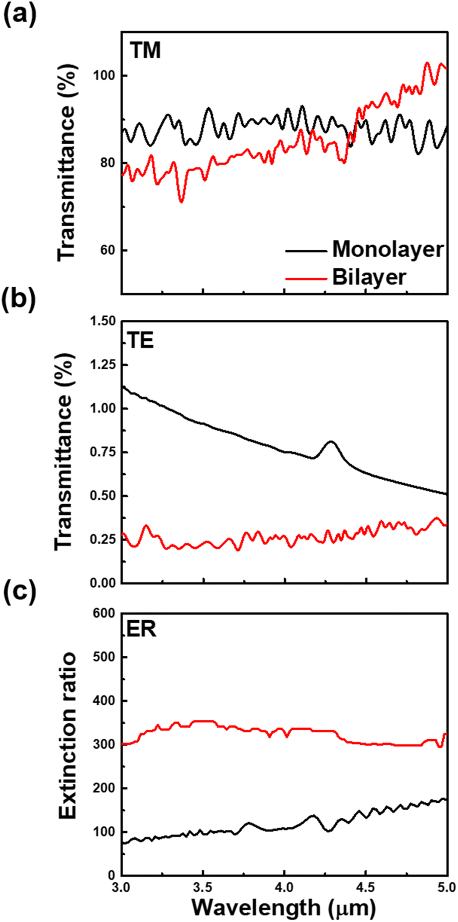
The transmittance measurement revealed no significant change in the TM transmittance in the two structures. The TE transmittance of the bilayer structure, however, exhibited a lower value than that of the monolayer structure. As illustrated in Fig. 7a and b, at a wavelength of 3.5 μm, the transmittance values of the TE light through the polarizer were approximately 0.91% and 0.23% for the monolayer and the bilayer, respectively. Evidently, the bilayer structure transmitted weaker TE waves than the monolayer structure because the laminated metal of the bilayer polarizer reflected most of the light waves, and consequently reduced the transmittance.21 Comparing the ER in terms of the structure, at 3.5 μm, the ER of the monolayer structure was 90, but the ER of the bilayer structure was 355, which is 4 times that of the monolayer.
 | ||
| Fig. 7 Experimental results of (a) TM, (b) TE, and (c) ER characteristics according to the structure. | ||
Theoretical (Fig. 5) and experimental (Fig. 7) characteristics have qualitatively consistent trends but significantly different quantitatively. For example, the theoretical ER in the bilayer structure is 1.2 × 10⁴ while the experimental ER in the bilayer structure is 355 at a wavelength of 3.5 μm. To confirm our speculation, we have employed Computer Simulation Technology Microwave Studio packages. It was carried out on the polarizer to investigate the effect of structure variation on its ER behaviour. In reality, ER properties could depend not only on the period of the wire grid, width of the wire, depth of the grid and metal thickness but also depend on microstructural features such as interface roughness, grain size and texture. Even though it was impossible to incorporate these details in our rather simplified modelling effort, we presume that the predicted ER values may at least serve as the upper bound values at each structure.
To maximize the polarizer performance, we fabricated an etched SiO2 post layer with a thickness of 350 nm through RIE. In this case, a local non-uniform etched area occurs through long-term etching. This inevitably degraded the etched SiO2 post layer surface smoothness at the top as well as on the side. Therefore, Au deposited on the etched SiO2 post has poor surface smoothness at the top and forms a sidewall, which scatters the light and reduces its transmittance, deteriorating the performance of the polarizer.22–25 Therefore, we attempted to improve the surface smoothness using the secondary etching technique. To reduce the surface roughness and sidewall, Ar ion milling was performed to etch the irregular shape of the metal. Because the dependence of surface properties on the ER is important for evaluating the performance of polarizers, the effect of surface properties on the ER was also studied.
Fig. 8 displays the scanning electron microscopy (SEM) image of the before-Ar-ion-milling surface with respect to the Ar-ion-milling time. To verify the change of surface roughness and sidewall, we conducted an experiment while increasing the milling time in 90 s increments. After the first 90 s, compared with those of the before-milling surface, the surface roughness and sidewall of the after-milling surface improved notably. However, the surface was still rough. An additional round of Ar ion milling was performed for 270 s, which significantly reduced the surface roughness and sidewall. However, the surface roughness and sidewall at 360 s were not significantly different from those at 270 s.
 | ||
| Fig. 8 SEM image of the surface of the bilayer wire-grid polarizer before and during Ar ion milling. | ||
Fig. 9a–c illustrate the simulation results of the light transmittance characteristics according to the surface roughness. As depicted in Fig. 9a and b, as the surface roughness was reduced, TM transmittance increased in the short-wavelength region. Thereafter, no significant change, or rather a subtle decrease in the long wavelength region, was observed. However, TE transmittance first plummets and subsequently declines gradually. The ER values at wavelengths of 3.5 and 4.5 μm obtained from the simulation results are illustrated in Fig. 6c. As indicated in the figure, the ER value increased as the surface became smoother for both the wavelengths, and the value gradually saturated as the roughness decreased further.
 | ||
| Fig. 9 Simulation results of (a) TM, (b) TE, and (c) ER characteristics according to surface roughness. Experimental results of the (d) TM, (e) TE, and (f) ER characteristics according to the Ar ion milling time. | ||
Fig. 9d–f depict the experimental results of transmittance according to the ion milling time. As indicated in the simulation result, with an increase in the milling time, TM transmittance increased, and TE transmittance declined. We confirmed that the surface roughness and sidewall decreased with the milling time. The transmittance measurements revealed that TM transmittance increased and TE transmittance decreased due to reduced light scattering. Hence, the ER increased. As depicted in Fig. 9f, the ER for the 360 s milled sample was 1255, which was markedly larger than those (460 and 600) of the 0- and 90 s milled samples, respectively. These results indicate that the Ar-ion-milled samples with enhanced surface smoothness exhibited an improved ER compared with the rough ones. Notably, the performance of the polarizer remarkably increased for smoother surfaces.
In general, bilayer wire-grid polarizers show better performance than monolayer polarizers, but the fabrication of bilayer polarizers has disadvantages in that it is difficult to manufacture because precise process control, complicated processes, and expensive process equipment are required. However, we were able to improve the performance of the bilayer wire-grid polarizer very easily by devising a method to improve the surface roughness using Ar ion milling to overcome the difficulties of fabrication of bilayer wire-grid polarizers with such high performance.
Conclusions
We theoretically and experimentally demonstrated a high-performance wire-grid polarizer using a dielectric material, a bilayer structure, and enhanced surface smoothness. The dielectric material absorbs the transmitted light and reduces loss. The bilayer structure allows the light reflected from the second grid to be partially re-reflected from the first grid, resulting in the F–P phenomenon caused by constructive or destructive interference. The enhanced surface smoothness reduces light scattering and increases transmittance. The material, structure, and smoothness increase the TM transmittance and decrease the TE transmittance, thereby increasing the ER and ultimately improving the performance of the wire-grid polarizer. These results will help design a polarizer structure that will maximize the polarization efficiency and realize a high-performance infrared polarized imaging system. The proposed method can be seamlessly extended to the development and optimization of optical, plasmonic, and polarization imaging systems where the polarizer is the most important component for achieving high-resolution and high-precision images.Author contributions
Conceptualization: Jiyeon Jeon, Byong Sun Chun and Youryang Seo; simulation: Jiyeon Jeon, Byong Sun Chun and Youryang Seo; writing—original draft preparation: Jiyeon Jeon, Byong Sun Chun and Youryang Seo; writing— review and editing: Minkyeong Kim, Hakseong Kim, Yeongho Kim, Jong Su Kim and Sang Jun Lee; supervision: Sang Jun Lee. All authors have read and agreed to the published version of the manuscript.Conflicts of interest
There are no conflicts to declare.Acknowledgements
This research was supported by Nano Material Technology Development Program (NRF-2018M3A7B4069994), National R&D Program (2022M3H4A1A02076394, 2022M3I8A2079227) through the National Research Foundation of Korea (NRF) funded by Ministry of Science and ICT and by Characterization platform for advanced materials funded by Korea Research Institute of Standards and Science (KRISS–2022–GP2022-0013).Notes and references
- K. P. Gurton, A. J. Yuffa and G. W. Videen, Opt. Lett., 2014, 39, 3857–3859 CrossRef PubMed.
- J. Hwang, B. Oh, Y. Kim, S. Silva, J. O. Kim, D. A. Czaplewski, J. E. Ryu, E. K. Kim, A. Urbas, J. Zhou, Z. Ku and S. J. Lee, Sci. Rep., 2018, 8, 14787 CrossRef PubMed.
- J. S. Tyo, D. L. Goldstein, D. B. Chenault and J. A. Shaw, Appl. Opt., 2006, 45, 5453–5469 CrossRef PubMed.
- C. S. L. Chun, D. L. Fleming and E. J. Torok, Proc. SPIE, 1994, 2234, 275–286 CrossRef.
- M. Felton, K. P. Gurton, J. L. Pezzaniti, D. B. Chenault and L. E. Roth, Opt. Exp., 2010, 18, 15704–15713 CrossRef CAS PubMed.
- J. Van der Spiegel, X. Wu, M. Zhang and N. Engheta, IEEE International Conference on Electron Devices and Solid State Circuit, EDSSC, 2012, pp. 1–3 Search PubMed.
- S. L. Wadsworth, P. G. Clem, E. D. Branson and G. D. Boreman, Opt. Mater. Express, 2011, 1, 466–479 CrossRef CAS.
- T. Du, F. Fan, A. M. W. Tam, J. Sun, V. G. Chigrinov and H. S. Kwok, Adv. Mater., 2015, 27, 7191–7195 CrossRef CAS PubMed.
- N. Nguyen-Huu, Y. L. Lo, Y. B. Chen and T. Y. Yang, Proc. SPIE, 2011, 7934, 79340U CrossRef.
- S. Ge, W. Liu, S. Zhou, S. Li, X. Sun, Y. Huang, P. Yang, J. Zhang and D. Lin, Coatings, 2018, 8, 192 CrossRef.
- Y. Lu, M. H. Cho, Y. P. Lee and J. Y. Rhee, Appl. Phys. Lett., 2008, 93, 061102 CrossRef.
- S. H. Ahn, J. S. Kim and L. J. Guo, J. Vac. Sci. Technol. B, 2007, 25, 2388–2391 CrossRef CAS.
- I. Yamada, K. Takano, M. Hangyo, M. Saito and W. Watanabe, Opt. Lett., 2009, 34, 274–276 CrossRef PubMed.
- Z. Li, W. Liu, H. Cheng, D. Y. Choi, S. Chen and J. Tian, Adv. Opt. Mater., 2019, 7, 1900260 CrossRef.
- Y. Ekinci, H. H. Solak, C. David and H. Sigg, Opt. Express, 2006, 14, 2323–2334 CrossRef CAS PubMed.
- T. Weiland, Arch. Elektron. Uebertrag., 1977, 31, 116–120 Search PubMed.
- J. J. Wang, W. Zhang, X. Deng, J. Deng, F. Liu, P. Sciortino and L. Chen, Opt. Lett., 2005, 30, 195–197 CrossRef PubMed.
- H. T. Chen, J. Zhou, J. F. O'Hara, F. Chen, A. K. Azad and A. J. Taylor, Phys. Rev. Lett., 2010, 105, 073901 CrossRef PubMed.
- J. Sun, L. Liu, G. Dong and J. Zhou, Opt. Express, 2011, 19, 21155–21162 CrossRef CAS PubMed.
- S. Im, E. Sim and D. Kim, Sci. Rep., 2018, 8, 14973 CrossRef PubMed.
- M. D. Islam, J. O. Kim, Y. Ko, Z. Ku, D. A. Boyd, E. M. Smith, V. Q. Nguyen, J. D. Myers, C. C. Baker, W. Kim, J. S. Sanghera, D. A. Czaplewski, A. M. Urbas, J. Genzer and J. E. Ryu, Macromol. Mater. Eng., 2020, 305, 2000033 CrossRef CAS.
- H. Ryu, S. J. Yoon and D. Kim, Appl. Opt., 2008, 47, 5715–5721 CrossRef CAS PubMed.
- T. Siefke, M. Heusinger, C. B. R. Hurtado, J. Dickmann, U. Zeitner, A. Tünnermann and S. Kroker, Opt. Express, 2018, 26, 19534–19547 CrossRef CAS PubMed.
- F. Zhang, J. Proust, D. Gérard, J. Plain and J. Martin, J. Phys. Chem. C, 2017, 121, 7429–7434 CrossRef CAS.
- H. Kim, S. Y. Ji, S. H. Cho, J. Y. Jung and W. S. Chang, Appl. Surf. Sci., 2022, 578, 151965 CrossRef CAS.
Footnote |
| † These authors contributed equally to this work. |
| This journal is © The Royal Society of Chemistry 2023 |