
 Open Access Article
 This Open Access Article is licensed under a Creative Commons Attribution-Non Commercial 3.0 Unported Licence
Nanoscale electrochemical charge transfer kinetics investigated by electrochemical scanning microwave microscopy†
Mohamed
Awadein
 a,
Maxwell
Sparey
a,
Simon
Grall
b,
Ferry
Kienberger
a,
Nicolas
Clement
b and
Georg
Gramse
*ac
a,
Maxwell
Sparey
a,
Simon
Grall
b,
Ferry
Kienberger
a,
Nicolas
Clement
b and
Georg
Gramse
*ac
aKeysight Labs Austria, Keysight Technologies, Linz 4020, Austria
bLIMMS/CNRS Institute of Industrial Science, University of Tokyo, Tokyo 153-8505, Japan
cInstitute of Biophysics, Johannes Kepler University, Linz 4020, Austria. E-mail: georg.gramse@jku.at
First published on 17th November 2022
Abstract
We show how microwave microscopy can be used to probe local charge transfer reactions with unprecedented sensitivity, visualizing surface reactions with only a few hundred molecules involved. While microwaves are too fast under classical conditions to interact and sense electrochemical processes, this is different at the nanoscale, where our heterodyne microwave sensing method allows for highly sensitive local cyclic voltammetry (LCV) and local electrochemical impedance spectroscopy (LEIS). LCV and LEIS allow for precise measurement of the localized charge transfer kinetics, as illustrated in this study for a ferrocene self-assembled monolayer immersed in an electrolyte. The theoretical analysis presented here enables a consistent mapping of the faradaic kinetics and the parasitic contributions (nonfaradaic) to be spectrally resolved and subtracted. In particular, this methodology reveals an undistorted assessment of accessible redox site density of states associated with faradaic capacitance, fractional surface coverage and electron transfer kinetics at the nanoscale. The developed methodology opens a new perspective on comprehending electrochemical reactivity at the nanoscale.
Introduction
The study of electron transfer kinetics in electrochemical reactions at the nanoscale has been hampered by instrumentation challenges related to tiny currents and small frequency bandwidth. Its understanding is essential for a range of applications including molecular electronics,1 material engineering,2 biosensors,3 photosynthesis,4 supercapacitors,5,6 and nanoelectronics devices7–10 such as DNA nanopores.11Established electrochemical methods, i.e. cyclic voltammetry (CV)12,13 and electrochemical impedance spectroscopy (EIS)7,14 are powerful techniques to study the potentiometric and kinetic aspects of charge transfer reactions in electrochemistry.
Although these classical methods provide access to important information about the ensemble of molecules, they are insensitive to surface heterogeneity. Scanning Electrochemical Microscopy (SECM)15–17 is a promising technique used to study electrochemical properties at the interfaces. SECM provides locally resolved surface analysis regardless of electrode conductivity. Even though the SECM is sensitive to heterogeneities throughout the sample surface, the image resolution is limited to the μm to sub-μm range.18 This barrier is due to the limitations in ultramicroelectrode (UME)19 fabrication methods. Atomic force microscopy-based SECM in molecular touching mode (Mt-AFM-SECM) is a desirable approach enabling electrochemical imaging at the nanoscale with fA resolution.20–22 However, it is limited in frequency bandwidth, and requires a redox cycling mechanism to operate (e.g. moving redox labeled molecules). Electrochemical-Scanning Tunneling Microscopy (EC-STM)23,24 is another high-resolution scanning probe microscopy (SPM) type that provides in situ monitoring of electrochemically active molecules.
The topographic resolution of EC-STM is in the sub-nm range, and the current sensitivity is within the sub-pA range. While this resolution is difficult to achieve with other techniques, the sensitivity is insufficient to measure current at the nanoscale. However, as we have shown previously, it is possible to go beyond this limitation and achieve aA (10−18 A)25 sensitivity by using a GHz heterodyne impedance sensing method combined with the EC-STM. This was technically realized by integrating a vector network analyzer (VNA) into EC-STM.25 We will refer to this new type of microscopy as Electrochemical Scanning Microwave Microscope (EC-SMM). The developed heterodyne impedance sensing methods have significant advantages compared to other methods in sensitivity (down to aA) and specificity (differential impedance is sensed) but also wide frequency bandwidth.
Based on this sensing mechanism, we develop in this study a closed theoretical framework that is used to quantitatively interpret the EC-SMM data and provide with this an extension of CV and EIS to the nanoscale. Our results show Localised Cyclic Voltammetry (LCV), derived from the RF-measurement signal while applying a potential linear sweep where we can distinguish between the resistive and capacitive contribution to the total current with an unparallel current sensitivity. Moreover, using EC-SMM, we demonstrate localized electrochemical impedance spectroscopy (LEIS) for the first time, allowing us to individually address the electrochemical process at the different frequency domains and helping us to eliminate the parasitic contribution.26,27 The analysis method accurately maps the nanoscale electron transfer kinetics related to the redox capacitance that previously studied and discussed in literature, but only based on macroscale measurements.28 Our electrochemical study was performed on Ferrocenyl-undecanethiol (FcC11SH) self-assembled monolayer (SAM) on gold electrode Au(111) as it provides an excellent platform for investigating electron transfer kinetics.29,30
Results and discussion
RF-electrochemical microscope
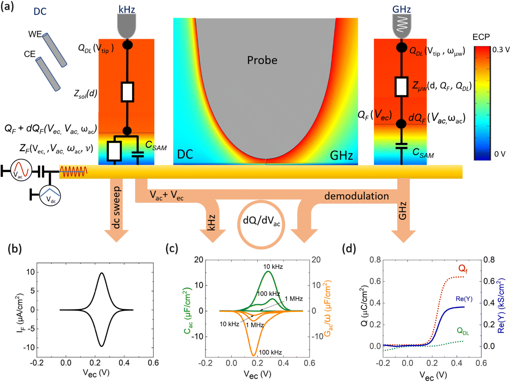
The EC-SMM merges the conventional EC-STM with the Scanning Microwave Microscopy (SMM).31,32 In EC-STM, a fixed bias potential is applied between the metallic probe and the conductive sample. The distance between probe tip and sample is in the range of 1–5 nm. For ideal topographical resolution, the tunnelling distances can be increased or reduced by increasing or lowering of the apparent tunnelling barrier height (the bias voltage) or by adjusting the tunneling current (setpoint). These parameters have to be adjusted depending on the SAM thickness under the tip. The resulting tunnelling current between the tip and the sample is used as distance feedback allowing for topographical imaging. The metallic tip is fully insulated apart from the apex, minimizing any parasitic current that obscures the tunnelling current. The bi-potentiostat controls the electrochemical potential between the two working electrodes, the sample (WE1) and the tip (WE2) with respect to the reference electrode. This allows maintenance of a constant potential between the sample and the tip while applying a linear potential sweep. The function of the bi-potentiostat is to keep the electrochemical background currents constant to ensure stable tunneling conditions. The VNA measures the reflection coefficient S11(ω, V) ∼ Z(ω, V), which is related to the impedance Z, as detailed in the Materials and Methods section.Probing charge dynamics of the solid–electrolyte-interface
Fig. 1a illustrates the area between the probe and redox-active self-assembled monolayer (SAM) on the gold substrate. It shows the distribution of the charges in the SAM-electrolyte interface, including the double layer and the associated diffusion layer at the SAM and probe interfaces. At GHz-frequencies Z = Zsol + ZSAM contain two contributions, a fully capacitive one from the SAM and a complex solution impedance. At a frequency much larger than the relaxation frequency, the SAM behaves mainly as a capacitor.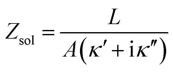 | (1) |
 | (2) |
 | (3) |
 | ||
| Fig. 1 Experimental setup and electrochemical model between the probe and the sample. (a) Shows a schematic model of the PtIr probe and the Fc SAM on Au(111) electrode separated by the NaCLO4, including the electrochemical double layers forming at the interfaces. The red and the blue areas represent the gradient of the positive and negative potentials. (b) Is the experimental setup of the broadband electrochemical microscope. A bi-potentiostat controls the dc potential of the probe and substrate. An additional ac perturbation voltage of 1–70 kHz is applied to the substrate by the lock-in. The VNA sends out a microwave signal to the probe. The back-reflected signal gets directly down-converted in the mixer and measured by the lock-in amplifier. | ||
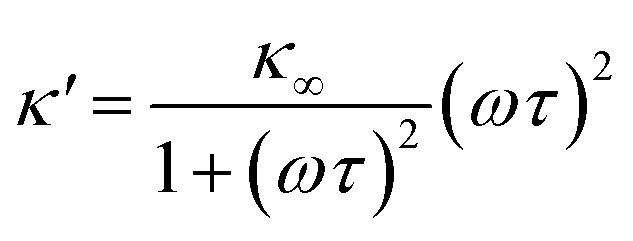
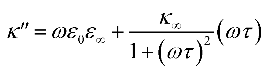
As eqn (2), (3) and Fig. S1† show, κ′ and κ′′ are strongly frequency dependent, where τ represents the Debye relaxation of the medium, κ∞,sol can be determined by κ∞,sol = εsε0/τ, εs = 78 which is the static dielectric constant, and ε0 = (8.85 × 10⁻¹²) F m−1 is the dielectric permittivity of vacuum. At low frequencies, the charges appearing on the ferrocene and the metallic probe are counterbalanced in the solution by ions that form the electrochemical double-layer extending with a length λD ∝ √c−1 into the electrolyte.
The Debye length λD is in the range of 10 nm for an ionic concentration of c = 1 mM in NaClO4 solution. Provided the ions can follow the alternating potential and are fast enough to diffuse in and out of the double layer, it acts as a pure capacitor Cdl(Q,ω). For frequencies slower than the relaxation time τdl = (λDL − λ2D) − (λSL)/D is typically defined by the distance between both electrodes L, the diffusion constant D, the Stern layer length λs, and the Debye length λD.34 This leads to a time constant of τdl = 106 ns or fdl ≈ 600 MHz (c = 1 mM, D = 1.85 × 10⁻⁹ m2 s−1, λD = 9.8 nm, L = 30 nm).35
Our SMM-STM probe operating at GHz frequencies and at very close proximity to the substrate (∼1–5 nm) has two important implications: (1) the double-layer capacitance is too slow to be sensed at GHz frequencies. (2) The separation distance between the two electrodes is smaller than the diffusion layer length, and thus the thin double layer approximation is no longer valid. Instead, the charges Q on the probe and the sample lead to an increase of the local ion concentration, c, and a decrease of the GHz impedance Z ∼ c as we will detail below.
Depending on the oxidation state of the surface-bound redox species on the sample side, they also expose a surface charge QF to the liquid interface, which is associated with a pseudo-or-faradaic capacitance CF.36
The faradaic charging current iF(t) of voltage V(t) applied across CF can be classically described by the following equation.29
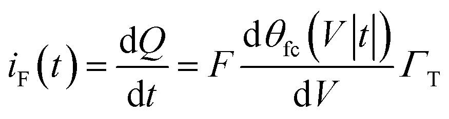 | (4) |
Γ T is the total surface coverage of ferrocene, θfc is the relative oxidation state, and F is the Faraday constant. CF is modulated by the ratio between oxidized and reduced species θfc. IF(t) is a result of the charge transfer from the gold substrate to the surface-bound electrochemical redox species across the alkyl chain, as shown in Fig. 1a. It is associated with a charge transfer resistance RCT. The following differential equation expresses the voltage dependency and the dynamics of θfc37
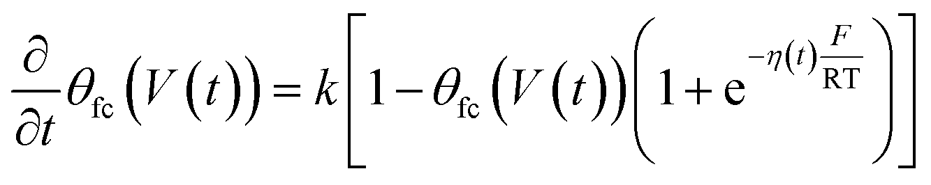 | (5) |
η(t) is the overpotential η(t) = V(t) − V(0), k is the reaction rate constant defined by 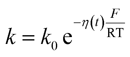 , with k0 the first order rate constant that includes a decay factor to account for the C11 thickness. The solution of this first-order differential equation (eqn (2)) gives the faradaic current induced by the potential linear sweep, as can be seen in Fig. 2b. Note that the CV's shape strongly depends on the sweep rate. For sweep rates or harmonic perturbations faster than k0 (i.e. GHz) or τF = RctCF the faradaic capacitance cannot charge anymore. For slower sweep rates, the current leads to charge QF(t) accumulation at the Fc–liquid interface, expressed with the following equation.
 | (6) |
 | ||
| Fig. 2 Finite element simulation (FEM) and equivalent circuit models resulting in global and localized CV curves. (a) The classical CV is obtained in the three-electrode configuration at mHz–Hz frequencies. Localized CVs are measured through variations of the GHz admittance Y (GHz, on the right) that are related with changes of the local ion concentration between probe and sample. The kHz modulation voltage Vac is used to probe ZF and its kinetics by demodulating dQ by dVac at ωac and considers the shown equivalent circuit. (b) Simulated global CV of the equivalent circuit (mHz–Hz domain). (c) Analytical simulation of dQ/dVac for ωac = 1, 10, 100 kHz corresponding to Cac and Gac/ωac. (d) Calculated double layer and faradaic charges (dotted lines) and corresponding Y change sensed at GHz frequencies (blue line). | ||
The presence of the charges at the solid electrolyte interface is associated with a local increase of the ion concentration and thus with a change in κ∞ by33
 | (7) |
Importantly, for frequencies close to the relaxation frequency of water, κ′ and κ′′ are both dependent on the ion concentration such that the impedance at GHz frequencies changes both its real and imaginary part (Z ∼ c). The number of charges that have to be compensated can be approximated using the image charge method by
| Q = QF(1 − ZSAM/Ztot) | (8) |
 | (9) |
Dynamics of the sample-probe system
Following this discussion on the charge sensing mechanism in the tip-sample region, we visualized the equivalent circuit models (Fig. 2) and the results of Finite Element Modelling (FEM) numerical simulations of the whole tip-sample region. The potential distribution around the tip-sample area is based on the Nernst–Planck–Poisson equations, calculated at quasi-static (DC) and GHz frequency conditions. The potential distribution is plotted together with the equivalent circuit models at different frequency domains, describing the electrochemical dynamics between the tip and the substrate, including the charging/discharging of the CF assessed by the EC-SMM. As can be seen from the FEM results (Fig. 2a), the electrical potential distribution at the probe liquid interface is different at DC potentials than at GHz potentials. The electrical double layer leads to an exponential potential drop at lower frequencies. At GHz, the effect is less pronounced. The equivalent circuit models differ depending on the frequency range. At low frequencies (mHz–Hz), where a potentiostat controls the voltage, the equivalent circuit model is represented by a solution impedance Zsol, a geometric capacitance (CSAM) for the SAM, and a faradaic impedance ZF(Vec) summarizing charge transfer resistance Rct and faradaic capacitance CF(Vec). A linear DC voltage sweep results in a current measured by the working electrode and leads to the CV shown in Fig. 2b which is described by eqn (5) and reflects the voltage dependency of Zf(Vec). As discussed above, the faradaic charge QF and the probe charges QP increases the local ion concentration, c, and thus decrease the impedance Zsol. The contribution of the different charges (dotted lines) is plotted against the applied electrochemical potential in Fig. 2d. As can be seen from eqn (9), the impedance decreases quickly with increasing tip-sample distances (see Fig. S2 and S3†). Only at <100 nm to the surface do the interface charges as a function of the redox charge become measurable.To isolate this signal with the EC-SMM an additional kHz voltage perturbation is applied to the substrate, this leads to dynamic oxidation and reduction of the ferrocene and charging/discharging of dQF. A lock in-amplifier (LIA) detects the change of the GHz wave impedance via and thus the derivative of the charge in the liquid between the probe and the ferrocene molecules.
 | (10) |
Note, that the measured charges correspond to the sum of probe (QP) and sample image charges (−QF):
| dQ = dQP(Rsol/Ztot) − dQf(1 − Rsol/Ztot) | (11) |
In Fig. 2c, we show the calculated Cac(Vec) and Gac(Vec) spectra based on eqn (1)–(8) for the one-dimensional case of a redox-active SAM with a thickness of 1.5 nm at a time constant of τF = 1 ms. As can be seen, Cac depends strongly on the sample electrochemical potential and also on the ac-modulation frequency. Thus, detecting the differential impedance gives us access to the LCV and LEIS. Additionally, all voltage-independent contributions are suppressed, which is the second significant advantage of differential measurement over absolute measurement leading also to an improved lateral resolution. In what follows, we will compare the modeling results with experimental data.
Localized cyclic voltammetry (LCV)
The EC-SMM allows us to study classical electrochemical and localized information simultaneously. The classical CV is shown in Fig. 3a and was obtained under potentiostatic control with a linear potential sweep applied between the substrate and the reference electrode. The current is measured at the substrate. As discussed earlier, this current relates to the electrochemical charge transfer, which oxidizes and reduces the surface-bound ferrocene molecules. We found that the maximum current of the classical CV (Fig. 3a) is Ip ≈ 0.6 μA cm−2, with a half-wave potential of E1/2 ∼ 0.24 V vs. Ag/AgCl, which leads to an average surface coverage of Γ = 2.4 ± 0.2 nm−2 being in agreement with literature.23 Simultaneously with the potential linear sweep, the STM probe recorded the Cac and Gac/ω that is plotted against the voltage sweep in Fig. 3b. The Cac signal measured at fac = 16 kHz resolves two arches at Vec ∼ 0.2 V and Vec ∼ 0.3 V. The first arch is due to the double-layer capacitance of the probe, and the second is due to the faradaic capacitance of the sample, as we showed in the theoretical calculations in Fig. 2c and d. Overall, the experimental data is in excellent qualitative agreement with the simulated data. Interestingly, the Gac/ω term of the complex capacitance in Fig. 3b, which corresponds to the loss term, shows a substantial variation during the voltage sweep.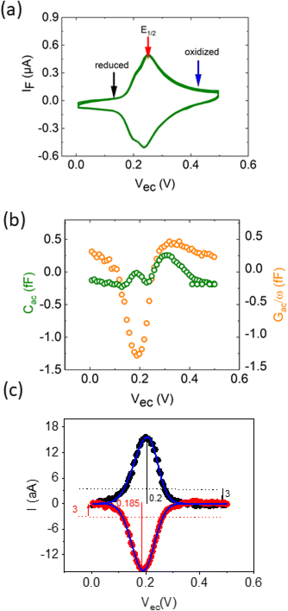 | ||
| Fig. 3 Comparison of classical and localized CV results. (a) The classical CV on an electrode area of 0.5 cm2 is shown. The CV is highly reversible, with a redox peak at ∼250 mV. The red and the black arrows mark the applied DC potential for LEIS. (b) Real and imaginary local capacitance sensed by the SMM. (c) The LCV curve is calculated from (b) as detailed in the text. All curves were recorded simultaneously at a potential sweep rate of 10 mV s−1. | ||
In Fig. 3c, we calculate from the measured data the corresponding local current of the LCV from the expression
| I = s(Cac − Gac/ω)/2 = sQ′ImZ′Re | (12) |
The overall shape of the global CV and local CV is similar; however, the local CV lacks the shoulder at ∼0.2 V which is related to the superposition of different organizational phases of Fc38 that are averaged in the global signal.
The forward/backward peak separation of LCV ΔEp ≈ 16 ± 2 mV is similar to the global CV, and the comparison of the faradaic currents from the global and local measurements allows us to determine the sensing area of the LCV more precisely to be A = 670 ± 15 nm2, what would be in line with an exposed probe radius of ∼15 nm (details on the calculation in ESI Note 1†).
Localized EIS
While the LCV allows us to study the dependency of the electrochemical charge transfer on the electrochemical potential, the kinetics can be addressed by local electrochemical impedance spectra (LEIS). Therefore, we acquired the LEIS of the Fc SAM in Fig. 4 a and b. The LEIS is represented in the bode diagram and Nyquist plot. The spectra were acquired at two steady-state potentials (marked in Fig. 3a). The red dots represent the impedance spectra at the potential of E1/2 and the blue dots at the oxidized state. At E1/2 the real part in the Bode plot shows one clear peak at around f2 = 16 kHz and indicates a second peak below our accessible frequency range (f1 < 1 kHz). The higher frequency f2 agrees approximately with the modulation frequency chosen for the LCV and explains the pronounced signal in the G/ωac channel in Fig. 3b.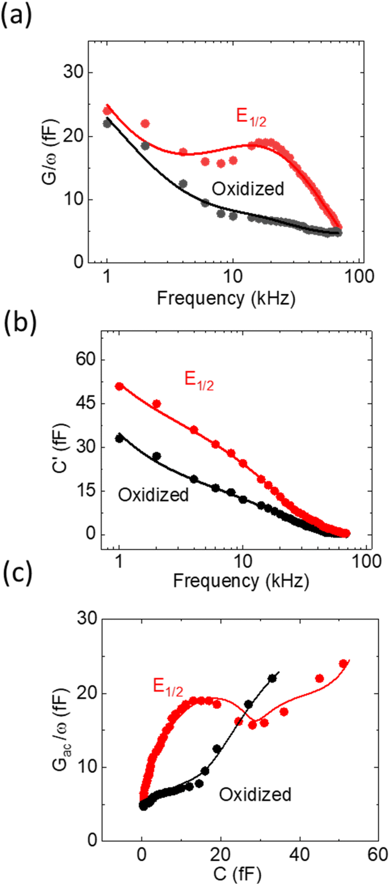 | ||
| Fig. 4 Experimental results DLEIS, fitted to the analytical simulation (a) and (b) are Bode plots of Cac and Gac/ω, the real and imaginary part of dQ/dV, respectively. The red circles and lines are the measured LEIS at E1/2 and the simulated data, respectively. The black circles and lines are measured LEIS at the oxidation potential and the simulated data. (c) is the Nyquist plot of (a) and (b). | ||
Interestingly, we note that the spectra acquired in the oxidized state show only the relaxation at f1 not the one at f2 like the curve acquired at E1/2. This can be understood considering the developed model in eqn (11) and allows us to extract quantitative values of the circuit parameters. Therefore, we model the total impedance according to the circuit in Fig. 2a with:
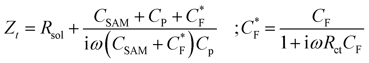 | (13) |
If we consider in this model the CSAM to be known (see Table 1), we can calculate the remaining parameters. As shown in the table, the values agree with literature23,32 using classical EIS. The most relevant parameter CF = 374 μF cm−2 at E1/2 already considers the coverage Γ. However, we note that the quantitative results depend strongly on the value chosen for CSAM. However, in the oxidized state, CF decreases as expected. Also, the charge transfer resistance Rct is within the range reported in the literature and decreases as expected in the oxidized state. Similar results are observed for the solution resistance that gets directly modulated by the charges on the Fc.
| Red | E 1/2 | Ox | Lit. | |
|---|---|---|---|---|
| a The used model is described in the text. We calculated CSAM assuming a thickness of 1.5 nm and an εr = 7, accounting for the coverage of the SAM. | ||||
| C p (μF cm−2) | 11 ± 3 | 14 ± 1.5 | 11 ± 1 | — |
| A s (μm2) | 0.038 ± 0.002 | — | ||
| C SAM (μF cm−2) | 8.18 | 1–16 (ref. 39 and 40) | ||
| C f (μF cm−2) | 74 ± 31 | 374 ± 55 | 134 ± 35 | 380 (ref. 41) |
| R ct (Ω cm2) | >1000 | 4 ± 2 | 1.6 ± 5 | 14 (ref. 41) |
| R s (Ω cm2) | 6.4 ± 10 | 8.7 ± 2 | 12 ± 5 | — |
Finally, the fit allows us to estimate the probing area As and the probe aperture radius for this measurement to be Rp = 35 ± 2 nm.
Conclusions
A heterodyne capacitive sensing method was proposed as a robust experimental technique in electrochemistry, from which a localized redox reaction can be resolved through localized cyclic voltammetry with sensitivity down to attoampere. This level of sensitivity is unparalleled by any other SPM technique. Additionally, localized EIS was performed for the first time by EC-SMM, enabling the study of the charge transfer kinetics at the nanoscale level. This technique has gone some way toward understanding the electrochemical process at nanoscale, as illustrated with an archetype molecular redox system. RF nano-electrochemistry and related analysis could have important implications for a better understanding of electrochemical catalysis at the nanoscale, batteries and charge transport in molecular biophysics.Materials and methods
Experimental setup
The experimental STM-SMM setup consists of a Keysight 5400 AFM operated in STM mode using Keysight STM scanner N9503A with a Pt/Ir probe (80/20). The STM scanner was modified by removing the front-end including the amplifier and replacing it with a modified SMA connector and a high quality coaxial cable that allows for stable connection of the STM probe and low loss transmission of the microwave to the probe. The STM probe was prepared by cutting 200 μm diameter Pt/Ir (80/20) wire and insulating it with apiezon wax. The bi-potentiostat system consisted of a Pt/Ir counter electrode (CE) (80/20), an Ag/AgCl reference electrode (RE), and an Au working electrode on a glass substrate (111) (Arrandee, Germany). The microwave excitation and sensing is done by a Keysight Vector Network Analyser (VNA) that is connected to the STM via a signal line using high quality coax cables. As shown in Fig. 1b, the microwave signal line includes an impedance matcher and directional coupler. A bias tee was used to separate the GHz high-frequency signal from the DC tunneling current that is measured by a FEMTO (109 Gain) current amplifier.Electrochemical methods
A single CV assessed the presence of ferrocene. This CV defined the redox potential with a measured E1/2 at ∼240 mV vs. Ag/AgCl (Fig. 3a). Following this, impedance measurements were carried out at the peak current potential and outside the redox window. DLEIS measurements were conducted by combining an AC signal (Vac) with a DC linear sweep and then applying the sum signal to the substrate. The AC signal Vac had an amplitude = 50 mV and a frequency range of 1–70 kHz. The modulated reflection coefficient S11 was demodulated by the lock-in amplifier. The output signal is the first derivative of S11, where the change in ΔS11 can be expressed as in the following equation (see ESI 3† for further information)| ΔS11 = AeiφΔZ(ω) = Aeiφ (R + 1/iωC) | (14) |
A defines the scaling of the admittance for the measured S11 signal, φ is the rotation in the complex plane. LEIS measurements were performed at two potential points to record the potential derivative of the impedance spectroscopy, dZ(ω)/dVac
Numerical calculation
FEM was performed with COMSOL Multiphysics 5.6 (2D axisymmetric, Nernst–Plank–Poisson Equations, statics, time domain, frequency domain perturbation). Simulation geometry resembles the experimental conditions shown in Fig. 2a. The model consisted of an STM probe modelled in a truncated conical shape with a cone angle of 15°. The tip has a spherical aperture with a radius of 100 nm located at a distance z above the sample. The SAM was defined as a dielectric layer with a thickness of 1.5 nm and dielectric permittivity of 2. The time-dependent charge at the interfaces of the SAM was calculated from eqn (3) using the boundary ODE interfaces. Meshing size was set to 0.1 nm on the apex of the probe and the SAM using the boundary layer mesh. The voltage sweep was applied to the probe, and the sample was identical to the experiment for the time-dependent solution. The upper side of the simulation box was set to the ground and acted as the reference electrode. The concentration on the upper side of the simulation box was set to 10 mM. To calculate the GHz capacitance, a harmonic perturbation of 10 mV was applied to the probe, and complex admittance was calculated. This model calculated the complex C(V) against voltage sweeps.The analytical modeling
The analytical modeling that resembles the experimental measurements was carried out with Wolfram Mathematica 12 and is based on the equivalent circuit model visualized in Fig. 2a. The double-layer was calculated from the Stern formula. The geometrical capacitance was defined as dielectric material with a thickness of 1.5 nm and dielectric permittivity of 2. The low-frequency dielectric permittivity of the electrolyte was set to 78. The tip-sample distance was defined as variable z (10–50 nm). The relaxation time of the electrolyte was set to 10 GHz. The faradaic current was obtained from the solution of the first-order differential eqn (2). The time-dependent voltage was defined as a superposition of linear potential sweep and the perturbation signal. The tip-sample capacitance and loss are calculated at 1 GHz and then demodulated by fitting with a harmonic function.Conflicts of interest
The authors declare no conflict of interest.Acknowledgements
This project has received funding from the MSCA-ITN projects BORGES and SENTINEL under grant agreements 813863 and 812398, respectively. Additional support from the NanoBat project funded by the EU's H2020 research and innovation program under Grant Agreements no. 861962 and the ATTRACT 2 project funded by European Commission under Grant Agreement 101004462 are acknowledged.References
- R. Sivakumarasamy, et al. , Selective layer-free blood serum ionogram based on ion-specific interactions with a nanotransistor, Nat. Mater., 2018, 17, 464–470 CrossRef CAS.
- M. Stefanoni, U. M. Angst and B. Elsener, Kinetics of electrochemical dissolution of metals in porous media, Nat. Mater., 2019, 18, 942–947 CrossRef CAS.
- A. Kyndiah, et al. , Nanoscale Mapping of the Conductivity and Interfacial Capacitance of an Electrolyte-Gated Organic Field-Effect Transistor under Operation, Adv. Funct. Mater., 2021, 31, 2008032 CrossRef CAS.
- K. K. Sakimoto, A. B. Wong and P. Yang, Self-photosensitization of nonphotosynthetic bacteria for solar-to-chemical production, Science, 2016, 351, 74–77 CrossRef CAS PubMed.
- P. K. Panda, A. Grigoriev, Y. K. Mishra and R. Ahuja, Progress in supercapacitors: roles of two dimensional nanotubular materials, Nanoscale Adv., 2020, 2, 70–108 RSC.
- F. Liu, et al. , Dual redox mediators accelerate the electrochemical kinetics of lithium-sulfur batteries, Nat. Commun., 2020, 11, 5215 CrossRef CAS PubMed.
- A. C. Meng, K. Tang, M. R. Braun, L. Zhang and P. C. McIntyre, Electrochemical impedance spectroscopy for quantitative interface state characterization of planar and nanostructured semiconductor-dielectric interfaces, Nanotechnology, 2017, 28, 415704 CrossRef.
- A. Alessandrini and P. Facci, Electron transfer in nanobiodevices, Eur. Polym. J., 2016, 83, 450–466 CrossRef CAS.
- J. Abbott, et al. , CMOS nanoelectrode array for all-electrical intracellular electrophysiological imaging, Nat. Nanotechnol., 2017, 12, 460–466 CrossRef CAS.
- A. Tarasov, et al. , Understanding the Electrolyte Background for Biochemical Sensing with Ion-Sensitive Field-Effect Transistors, ACS Nano, 2012, 6, 9291–9298 CrossRef CAS.
- C. Lv, et al. , Molecular Transport through a Biomimetic DNA Channel on Live Cell Membranes, ACS Nano, 2020, 14, 14616–14626 CrossRef PubMed.
- N. Elgrishi, et al. , A Practical Beginner's Guide to Cyclic Voltammetry, J. Chem. Educ., 2018, 95, 197–206 CrossRef CAS.
- C. Yun and S. Hwang, Analysis of the Charging Current in Cyclic Voltammetry and Supercapacitor's Galvanostatic Charging Profile Based on a Constant-Phase Element, ACS Omega, 2021, 6, 367–373 CrossRef CAS.
- B.-Y. Chang and S.-M. Park, Electrochemical Impedance Spectroscopy, Annu. Rev. Anal. Chem., 2010, 3, 207–229 CrossRef CAS PubMed.
- C. Sandford, et al. , A synthetic chemist's guide to electroanalytical tools for studying reaction mechanisms, Chem. Sci., 2019, 10, 6404–6422 RSC.
- M. A. Edwards, S. Martin, A. L. Whitworth, J. V. Macpherson and P. R. Unwin, Scanning electrochemical microscopy: principles and applications to biophysical systems, Physiol. Meas., 2006, 27, R63–R108 CrossRef PubMed.
- K. Eckhar, X. Chen, F. Turcu and W. Schuhmann, Redox competition mode of scanning electrochemical microscopy (RC-SECM) for visualisation of local catalytic activity, Phys. Chem. Chem. Phys., 2006, 8, 5359 RSC.
- A. J. Bard and M. V. Mirkin, Scanning electrochemical microscopy, CRC Press, 2001 Search PubMed.
- J. Op de Beeck, W. De Malsche, D. S. Tezcan, P. De Moor and G. Desmet, micro-fabrication processes on the, J. Chromatogr. A, 2012, 1239, 35–48 CrossRef CAS PubMed.
- K. Huang, A. Anne, M. A. Bahri and C. Demaille, Probing Individual Redox PEGylated Gold Nanoparticles by Electrochemical–Atomic Force Microscopy, ACS Nano, 2013, 7, 4151–4163 CrossRef CAS.
- L. Nault, et al. , Electrochemical Atomic Force Microscopy Imaging of Redox-Immunomarked Proteins on Native Poxviruses: From Subparticle to Single-Protein Resolution, ACS Nano, 2015, 9, 4911–4924 CrossRef CAS.
- K. Chennit, et al. , Electrochemical Imaging of Dense Molecular Nanoarrays, Anal. Chem., 2017, 89, 11061–11069 CrossRef CAS.
- A. K. Yagati, J. Min and J.-W. Choi, Electrochemical Scanning Tunneling Microscopy (ECSTM) – From Theory to Future Applications, in Modern Electrochemical Methods in Nano, Surface and Corrosion Science, ed. Aliofkhazraei M., InTech, 2014 Search PubMed.
- M. López-Martínez, et al. , Differential Electrochemical Conductance Imaging at the Nanoscale, Small, 2017, 13, 1700958 CrossRef.
- S. Grall, et al. , Attoampere Nanoelectrochemistry, Small, 2021, 17, 2101253 CrossRef CAS.
- P. F. Barbara, T. J. Meyer and M. A. Ratner, Contemporary Issues in Electron Transfer Research, J. Phys. Chem., 1996, 100, 13148–13168 CrossRef CAS.
- P. R. Bueno, G. Mizzon and J. J. Davis, Capacitance Spectroscopy: A Versatile Approach To Resolving the Redox Density of States and Kinetics in Redox-Active Self-Assembled Monolayers, J. Phys. Chem. B, 2012, 116, 8822–8829 CrossRef CAS.
- C. E. D. Chidsey, Free Energy and Temperature Dependence of Electron Transfer at the Metal-Electrolyte Interface, Science, 1991, 251, 919–922 CrossRef CAS.
- A. L. Eckermann, D. J. Feld, J. A. Shaw and T. J. Meade, Electrochemistry of redox-active self-assembled monolayers, Coord. Chem. Rev., 2010, 254, 1769–1802 CrossRef CAS.
- K. Uosaki, Y. Sato and H. Kita, Electrochemical characteristics of a gold electrode modified with a self-assembled monolayer of ferrocenylalkanethiols, Langmuir, 1991, 7, 1510–1514 CrossRef CAS.
- B. A. Bagdad, C. Lozano and F. Gamiz, Near-field scanning microwave microscope platform based on a coaxial cavity resonator for the characterization of semiconductor structures, Solid-State Electron., 2019, 159, 150–156 CrossRef CAS.
- S. Berweger, et al. , Microwave Near-Field Imaging of Two-Dimensional Semiconductors, Nano Lett., 2015, 15, 1122–1127 CrossRef CAS PubMed.
- V. V. Shcherbakov, Y. M. Artemkina, I. A. Akimova and I. M. Artemkina, Dielectric Characteristics, Electrical Conductivity and Solvation of Ions in Electrolyte Solutions, Materials, 2021, 14, 5617 CrossRef CAS PubMed.
- M. Z. Bazant, K. Thornton and A. Ajdari, Diffuse-charge dynamics in electrochemical systems, Phys. Rev. E, 2004, 70, 021506 CrossRef.
- K. Hu, Z. Chai, J. K. Whitesell and A. J. Bard, In situ monitoring of diffuse double layer structure changes of electrochemically addressable self-assembled monolayers with an atomic force microscope, Langmuir, 1999, 15(9), 3343–3347 CrossRef CAS.
- B. E. Conway and E. Gileadi, Kinetic theory of pseudo-capacitance and electrode reactions at appreciable surface coverage, Trans. Faraday Soc., 1962, 58, 2493 RSC.
- B. E. Conway, V. Birss and J. Wojtowicz, The role and utilization of pseudocapacitance for energy storage by supercapacitors, J. Power Sources, 1997, 66, 1–14 CrossRef CAS.
- C. Cannes, F. Kanoufi and A. J. Bard, Cyclic voltammetry and scanning electrochemical microscopy of ferrocenemethanol at monolayer and bilayer-modified gold electrodes, J. Electroanal. Chem., 2003, 547, 83–91 CrossRef CAS.
- Y. Aceta, Y. R. Leroux and P. Hapiot, Evaluation of Alkyl-Ferrocene Monolayers on Carbons for Charge Storage Applications, a Voltammetry and Impedance Spectroscopy Investigation, ChemElectroChem, 2019, 6, 1704–1710 CrossRef CAS.
- F. S. Damos, R. C. S. Luz and L. T. Kubota, Determination of Thickness, Dielectric Constant of Thiol Films, and Kinetics of Adsorption Using Surface Plasmon Resonance, Langmuir, 2005, 21, 602–609 CrossRef CAS.
- P. R. Bueno and J. J. Davis, Elucidating Redox-Level Dispersion and Local Dielectric Effects within Electroactive Molecular Films, Anal. Chem., 2014, 86, 1997–2004 CrossRef CAS PubMed.
Footnote |
| † Electronic supplementary information (ESI) available. See DOI: https://doi.org/10.1039/d2na00671e |
| This journal is © The Royal Society of Chemistry 2023 |