
 Open Access Article
 This Open Access Article is licensed under a Creative Commons Attribution-Non Commercial 3.0 Unported Licence
The growth mechanism and intriguing optical and electronic properties of few-layered HfS2†
Jitendra
Singh
*ab,
Jia-Hui
Shao
a,
Guan-Ting
Chen
a,
Han-Song
Wu
a and
Meng-Lin
Tsai
 *a
*a
aDepartment of Materials Science and Engineering, National Taiwan University of Science and Technology, Taipei 106335, Taiwan
bDepartment of Physics, Udit Narayan Post Graduate College Padrauna, Kushinagar 274304, Uttar Pradesh, India
First published on 7th November 2022
Abstract
Due to electronic properties superior to group VIB (Mo and W) transition metal dichalcogenides (TMDs), group IVB (Hf and Zr) TMDs have become intriguing materials in next-generation nanoelectronics. Therefore, the growth of few-layered hafnium disulfide (HfS2) on c-plane sapphire as well as on a SiO2/Si substrate has been demonstrated using chemical vapour deposition (CVD). The structural properties of HfS2 were investigated by recording X-ray diffraction patterns and Raman spectra. The XRD results reveal that the layers are well oriented along the (0001) direction and exhibit the high crystalline quality of HfS2. The Raman spectra confirm the in-plane and out-plane vibration of Hf and S atoms. Moreover, the HfS2 layers exhibit strong absorption in the UV to visible region. The HfS2 layer-based photodetector shows a photoresponsivity of ∼1.6, ∼0.38, and ∼0.21 μA W−1 corresponding to 9, 38, and 68 mW cm−2, respectively under green light illumination and is attributed to the generation of a large number of electron–hole pairs in the active region of the device. Besides, it also exhibits the highly crystalline structure of HfS2 at high deposition temperature. The PL spectrum shows a single peak at ∼1.8 eV and is consistent with the pristine indirect bandgap of HfS2 (∼2 eV). Furthermore, a few layered HfS2 back gate field-effect transistor (FET) is fabricated based on directly grown HfS2 on SiO2/Si, and the device exhibits p-type behaviour. Thus, the controllable and easy growth method opens the latest pathway to synthesize few layered HfS2 on different substrates for various electronic and optoelectronic devices.
1. Introduction
In recent years, two-dimensional (2D) materials, particularly graphene, have attracted widespread attention due to their physical and chemical properties.1–3 However, the zero bandgap in graphene limits its utility for various electronic and optoelectronic applications. This has aroused interest in other materials with inherent 2D bandgaps, such as hexagonal boron nitride, black phosphorous, and transition metal dichalcogenides (TMDs).4–6 Among them, group VIB TMD monolayers and few-layered MX2 (where M = transition metal, X = S, Se, and T) have been exclusively investigated and become potential candidates for different electronic and optoelectronic devices.7–10 Besides, group IVB (HfX2, ZrX2, X = S, Se) monolayers and few layers are seldom reported but have remarkable electronic and optoelectronic properties.11–16 An acoustic phonon-limited carrier mobility of ∼1800 cm2 V−1 s−1 is calculated theoretically at room temperature for HfS2, which is far higher compared to that of the widely investigated MoS2 (∼340 cm2 V−1 s−1).16 Moreover, theoretical calculations also revealed that field-effect transistors (FETs) based on HfS2 can have a sheet current density of ∼500 μA μm−1, which is ∼102 times higher than that of FETs based on MoS2.17 Thus, HfS2 has emerged as a promising material with great potential for electronic and optoelectronic applications.18,19Despite remarkable predictions based on theoretical calculations, only a handful of experimental results have been reported. This is due to the adversities involved in the growth of HfS2 monolayers and few layers. Previously, mechanical exfoliation methods were utilized to develop few-layered HfS2 based ultrasensitive phototransistors and efficient FETs.11,12 However, mechanical exfoliation methods lead to uncontrolled formation of a number of layers which hinders the comprehensive study of HfS2-based phototransistors. On the other hand, the chemical vapour deposition (CVD) technique has been widely reported as a potential method for synthesizing large area 2D monolayers such as MoS2,20 WS2,21 and ZrS2.22 Recently, epitaxial growth of high quality HfS2 on the c-plane sapphire substrate has been demonstrated using CVD.18 However, the optimal device performance based on epitaxial growth has still not been achieved. In particular, HfS2 (∼1.33 eV per primitive cell)23 has larger interaction energy than MoS2 (∼0.46 eV per primitive cell),21 which affects the substrate surface energy. Thus, the transfer of effective atoms is strongly hindered which results in the vertical formation of a film. This kind of structure is not suitable for fabricating electronic or optoelectronic devices.24 Until now, there have been no reports on direct growth of HfS2 on the SiO2/Si substrate using CVD, which is a crucial requirement for the fabrication of various electronic and optoelectronic devices.25,26 Generally, it has been reported that as-grown HfS2 on sapphire can be subsequently transferred to the SiO2/Si substrate using dry and wet transfer methods. However, this brings side effects (strain and doping) due to the contamination of (and deterioration of) as-grown HfS2, which leads to altering of the pristine electronic structure. Thus, the growth of high quality HfS2 either on c-sapphire or directly on SiO2/Si is still a demanding task for fabricating highly efficient and stable electronic and optoelectronic devices.
To avoid the aforementioned issues, in this work, few-layered HfS2 films have been successfully grown on c-plane sapphire and directly on the SiO2/Si substrate through CVD using hafnium tetra-chloride (HfCl4) and sulfur (S) as reactants. The few-layered films show high crystallinity and edge orientation. Furthermore, a photodetector has been fabricated using as-grown HfS2 on c-plane sapphire and it exhibits a good photoresponse of ∼1.6, ∼1.5, and ∼1.4 μA W−1 under green, UV, and white light illumination conditions, respectively at a power density of 9 mW cm−2. The photodetector also reveals a fast rise time of 0.33 s and recovery time of 0.40 s under green light illumination. These values are very close to the previously reported values in the case of vertically oriented few-layered HfS2 nanosheet-based photodetectors.11,24 The fast rise and recovery times of our device are attributed to the presence of low defect density and trap states at the interface which leads to prompt charge carrier separation in the active region of the device. These results suggest that HfS2 can be a suitable material for various electronic and optoelectronic applications. Keeping these applications of HfS2 in mind, therefore, we have fabricated a back-gate FET based on few-layered HfS2 directly grown on the SiO2/Si substrate, and the device exhibits p-type behaviour. We believe that this is the first time direct growth of few-layered HfS2 on the SiO2/Si substrate using CVD for the fabrication of back-gate FETs has been reported. Thus, this controllable approach of CVD provides a new route to direct growth of few-layered HfS2 on the SiO2/Si substrate for various promising, highly efficient, and stable electronic and optoelectronic devices.
2. Experimental methods
2.1 Sample preparation
Few-layered HfS2 on c-plane sapphire and SiO2/Si substrates was synthesized using the chemical vapour deposition (CVD) technique in a hot wall furnace as shown in Fig. 1(a). 200 mg of high purity sulfur powder (99%, Showa) and 100 mg of HfCl4 (98%, Sigma Aldrich) were placed in two separate Al2O3 crucibles and inserted upstream at the low heating zone. Pre-ultra-sonication cleaned c-sapphire and SiO2/Si (300 nm) substrates (acetone, IPA, DI water for each 15 min, dry under N2 gas) were used to grow few-layered HfS2. First, the c-sapphire substrate was placed at a heating zone 3 cm behind the sensor and few-layered HfS2 was successfully grown in the upstream. Similarly, the SiO2/Si substrate was inserted at the same place and the upstream growth of few-layered HfS2 was carried out. The pressure in the tube was 15 Torr and then 100 sccm Ar and 10 sccm H2 were pumped into the tube. The temperatures of the high and low heating zone were kept at 950 °C and 200 °C, respectively. The high temperature zone was heated at 25 °C min−1 from room temperature to 950 °C and it took 37 minutes to reach the appropriate temperature, while for the low temperature zone, 37 minutes was set to reach 200 °C. The growth time was kept at 25 min. After completion of growth in 25 min, both heating zones were stopped and immediately the furnace was opened for cooling. After rapid cool down of the furnace, the samples were taken out for further characterization. | ||
| Fig. 1 (a) Schematic illustration of chemical vapor deposition (CVD) growth of few-layered HfS2 in high and low temperature zones. (b) The temperature profiles of low and high temperature zones during the growth process of HfS2. (c) and (d) Side and top views of the hexagonal structure of HfS2. | ||
2.2 Calculation details
The calculations were performed mainly with the Biovia Material Studio CASTEP code (Accelrys Inc., San Diego, CA, USA).27,28 The generalized gradient approximation functional (GGA) was parameterized by Perdew, Burke, and Ernzerhof.29 The plane-wave cut-off energy was set to 400 eV and shifted 4 × 4 × 2 Monkhorst–Pack meshes for the layered structures were used. Also, 4 × 4 × 2 meshes with actual spacing 0.079233, 0.079233, and 0.3879, respectively, for the bulk, were used to perform Brillouin zone integration in order to ensure the convergence of the results. A tolerance SCF factor of 2 × 10⁻⁶ eV per atom was used to perform the calculations. The convergence of the total energy was set to be better than 2 × 10⁻⁵ eV per atom. A vacuum layer with a thickness of 10 Å was used to model the 2D nature of the compounds.2.3 Device fabrication
Photodetectors based on few-layered HfS2 grown on c-plane sapphire were fabricated by depositing Ni (50 nm) contacts using RF sputtering (multi-functional sputtering, KD-sputter R-24K11) through a shadow mask under a high vacuum and a pressure of 5 × 10⁻⁶ Torr at room temperature. The photoresponse of the device was measured using a Keithly 2612 B source meter under various light illumination conditions such as UV, green, and white. Further, a few layered HfS2 based back-gate FETs were fabricated on directly grown few-layered HfS2 on SiO2/Si by depositing Ni (5 nm)/Au (95 nm) contacts using an e-gun (Fulintec, FU-12CE) through a shadow mask at room temperature with a pressure of 4 × 10⁻⁴ Torr. The current–voltage (I–V) characteristics of the device were measured by using a Keithley 2612B source meter at a different gate and drain bias voltage.2.4 Characterization
The XRD patterns of as grown few-layered HfS2 on c-plane sapphire and SiO2/Si substrates were recorded using a Bruker D2 phaser X-ray diffractometer setup. The Raman spectra of HfS2 on both substrates were recorded using a HORIBA (iHR550) micro-Raman spectrometer. The topography and thickness of few-layered HfS2 were measured in tapping mode through atomic force microscopy (AFM) using a Bruker Dimension ICON setup. The TEM images of HfS2 were characterized using a Philips Tecnai F30 Field Emission Gun Transmission Microscope (FEG-TEM) operating at 200 kV. The sample was first transferred onto a copper grid and then images were recorded for characterization. The X-ray photoemission spectroscopy (XPS) measurements were performed using a VG ESCA Scientific Theta Probe with Al Kα (1486.6 eV) with an X-ray spot size of 15–400 μm. The absorbance spectra (from 200–800 nm range) and PL spectra (under 460 nm excitation) of few-layered HfS2 were investigated using a UV-vis-NIR spectrophotometer (JASCO V670) and a fluorescence spectrometer (JASCO FP-8500) with an integrating sphere, respectively.3. Results and discussion
The growth of few-layered HfS2 on c-plane sapphire and SiO2/Si substrates was carried out using a CVD system with a separate heating zone as represented by the schematic in Fig. 1(a). Contrary to most CVD syntheses of TMDs, hafnium dioxide (HfO2) was not taken into consideration as a reactant material for use as a source of hafnium since its evaporation temperature is too high (∼2500 °C). As an alternative, we decided to use hafnium tetrachloride (HfCl4), which has a low sublimation temperature (∼317 °C), as a precursor.Due to the low melting point of HfCl4, it is beneficial for synthesizing HfS2 films under more uniform and stable growth conditions during the CVD process. Briefly, S and HfCl4 powders were used as precursors and put in separate crucibles and then inserted inside a quartz tube. Appropriate substrates were placed in the high temperature heating zone. Before the growth process, c-plane sapphire and SiO2/Si substrates were pre-cleaned to avoid the contamination and formation of defect and trap states at the surface during the growth process. Typical growth temperatures were set at 950 °C and 200 °C for high and low heating zones, respectively. The growth pressure was controlled at 15 Torr. The growth time was varied between 15 and 25 minutes for different thicknesses of HfS2, and 100 sccm Ar and 10 sccm H2 were used as carrier gases during the growth process. By using these obtained parameters, it was observed that the evaporation of the source has more control since it simply depends on the precursor and carrier gas flow rates. It is noticed that the hydrogen gas flow is crucial for the sulfurization of HfCl4. Thus, in our experiment, the growth of HfS2c-plane sapphire and SiO2/Si substrates cannot be achieved if we do not use hydrogen gas as a strong additional reductant. A potential reaction is as follows:
| HfCl4 (g) + 2S (g) 2H2 (g) → HfS2 (g) + 4HCl (g) | (1) |
The samples were cooled down from 950 °C to room temperature under Ar gas flow immediately after the growth process. The growth and cooling temperature profiles are illustrated in Fig. 1(b). As-grown HfS2 on sapphire and SiO2/Si substrates was investigated by optical microscopy and the optical images are shown in Fig. S1(a) and (b), respectively in the ESI.† HfS2 on sapphire exhibits yellowish color while that on the SiO2/Si substrate shows a faded pink color, illustrating good uniformity and continuity via our CVD technique. It was noticed that the growth of HfS2 on sapphire was easily achieved due to the presence of fewer dangling bonds on the surface of sapphire as a result of the lower energy barrier for the migration of HfS2 along the substrate leading to the uniform and continuous layer formation of HfS2. However, the basic growth mechanism of HfS2 on the SiO2/Si substrate is as follows: in the initial reaction stage, first S, vapor of HfCl4, and hydrogen react with each other at appropriate temperatures and form HfS2 species which diffuse simultaneously onto the SiO2/Si substrate. Later, HfS2 species that are adsorbed on the substrate then attempt to migrate to form the HfS2 layer. But the presence of dangling bonds at the surface of SiO2/Si substrate increases the energy barrier for the migration of HfS2 along the substrate surface and hinders the formation of HfS2 monolayers on the substrate.24 The adatoms–substrate interaction and the concentration gradient of the adatoms both have a significant impact on the surface migration of HfS2.24 As a result, the 1T-HfS2 interlayer interaction energy, which is 1.33 eV per primitive cell, is significantly higher than that of MoS2 (0.46 eV per primitive cell)21 and a low diffusion flux of gaseous HfS2 species that form the vapor phase at the start of the reaction efficiently shortens the migration length, which results in the formation of 3D fracture like layers of HfS2 on the SiO2/Si substrate. The height of HfS2 nanoparticles is confined to a limited nucleation time before covering the entire surface of a substrate. However, to gain an in-depth understanding of this growth mechanism on the SiO2/Si substrate further experimental work will be needed.
Fig. 1(c) and (d) show the top and side views of an atomistic model of HfS2 in which each layer contains three atomic planes. The Hf atoms are octahedrally coordinated by six S atoms that are covalently bonded in the order S–Hf–S with a thickness of ∼0.59 nm controlled by weak vdW interactions. HfS2 acquires a CdI2 like structure (1T structure) and belongs to space group P![[3 with combining macron]](https://www.rsc.org/images/entities/char_0033_0304.gif) m1 with a cell dimension a = b = 3.625 Å and c = 5.846 Å.30
m1 with a cell dimension a = b = 3.625 Å and c = 5.846 Å.30
As grown few-layered HfS2 on c-plane sapphire and SiO2/Si substrates was characterized for its structural properties by performing Raman and X-ray diffraction (XRD) measurements. The Raman spectra of as-grown HfS2 on sapphire and SiO2/Si substrates were recorded using a 532 nm excitation laser as shown in Fig. 2(a) and (b), respectively, which exhibit two characteristic peaks at ∼264 cm−1 and ∼338 cm−1 attributed to the Eg and A1g modes, corresponding to the in-plane and out of plane vibration modes of the S–Hf–S lattice, respectively.31,32 The Raman modes are consistent with that reported for mechanical exfoliated thin films.23 The full width at half maximum (FWHM) value of the A1g Raman mode is less than 10 cm−1, indicating the high crystal quality of HfS2.27 Similarly, the XRD patterns of as-grown HfS2 on c-plane sapphire and SiO2/Si substrates were obtained in a normal θ–2θ configuration as shown in Fig. 2(c) and (d), respectively. The XRD pattern on both the substrates is composed of various peaks which correspond to the characteristic peaks of HfS2. All peaks have been allocated their identification and Miller indices. Despite the sapphire peak (0006) (Fig. 2(c)) from the substrate, only the (000l) diffraction peaks of the 1T phase of HfS2 are distinctly found at 2θ = 15.1°, 30.5°, 46.6°, and 63.5°, corresponding to (0001), (0002), (0003), and (0004) of HfS2 (JCPDS card No. 28-0444), respectively, showing that the HfS2 layers were grown in the c-plane axis of the sapphire substrate. All HfS2 peaks were also clearly observed on the SiO2/Si (Fig. 2(d)) substrate. The XRD peaks of HfS2 on both SiO2/Si and sapphire substrates are well matched with the reported characteristics peaks of HfS2 in the literature.27 The sharp and narrow peaks with a FWHM of <0.3° represent the high crystalline quality of HfS2 on both substrates.
 | ||
| Fig. 2 (a) Raman spectra of as grown-HfS2 on (a) sapphire and (b) SiO2/Si substrates. X-ray diffraction patterns of HfS2 grown on (c) sapphire and (d) SiO2/Si substrates. (e) UV-visible spectra: black (theoretical) and red (experimental) and (f) Tauc plot of as grown few-layered HfS2 on sapphire to estimate the optical bandgap. | ||
The intriguing optical properties of HfS2 grown on sapphire were investigated by performing UV-visible measurements as shown in Fig. 2(e). The absorption spectra exhibit broad range absorbance in the UV to visible (300–600 nm) region. The spectra are quite well matched with the theoretical absorption of HfS2. The absorption peak is observed around 440 nm, representing the opening of the optical bandgap in HfS2. An optical bandgap of ∼2.59 eV is estimated from the absorption band edge using the Tauc plot as shown in Fig. 2(f). The calculated band structure of bulk HfS2 using various theoretical methods predicted indirect bandgaps of 1.9 and 2.7 eV,33 while the bandgap of bulk HfS2 calculated from experimental methods was found to be about 2 eV.34,35 This inequality of bandgaps between the current study and previously reported studies could be ascribed to the quantum confinement effect as investigated earlier in the case of MoS2.36 The photoluminescence (PL) spectrum of HfS2 grown on SiO2/Si was obtained and is shown in Fig. S2 in the ESI,† which exhibits the main peak at ∼659 nm (1.88 eV), which is very close to the theoretically predicted bandgap of HfS2. This peak is attributed to the near bandgap emission of HfS2 since it is very close to the bandgap. The PL spectrum also consists of a peak at a higher wavelength of ∼670 nm (1.85 eV) and is probably attributed to defect related emission. However, further examination is still needed to confirm the exact origin of this peak.
The surface topography of as grown few-layered HfS2 on sapphire and SiO2/Si was investigated by recording atomic force microscopy (AFM) images shown in Fig. 3(a) and (b), respectively. The AFM results reveal a root mean square (RMS) of ∼4 nm for the few-layered HfS2 surface on sapphire. Besides, a uniform terraced structure along a sharp edge can be distinctly found (Fig. 3(a)). The step height profiles at the terrace edge of few layered HfS2 on sapphire and SiO2/Si are shown in Fig. 3(c) and (d), respectively, in which the terrace height is determined to be ∼21 and ∼25 nm, on sapphire and SiO2/Si, respectively. Moreover, the terrace edge is oriented with a dominant direction, revealing the preferential orientation of grown HfS2. Further, the elemental composition and bonding type in HfS2 were investigated by performing X-ray photoelectron spectroscopy (XPS) measurements. The binding energy peaks observed near 17.6 eV and 16.2 eV are shown in Fig. 4(a) and can be attributed to Hf 4f5/2 and 4f7/2 core levels. The binding energy peaks observed near 162.0 and 160.2 eV in Fig. 4(b) correspond to S 2p1/2 and 2p3/2 core levels. These peak positions are well matched with the reported standard spectra of HfS2.37 Thus, the results justified the growth of few layered HfS2 by CVD. Besides, the signal due to the chlorine (Cl) element is entirely suppressed exhibiting the complete reaction of HfCl4 to form HfS2 during the CVD process as shown in Fig. S2(b) and (c) in the ESI.†
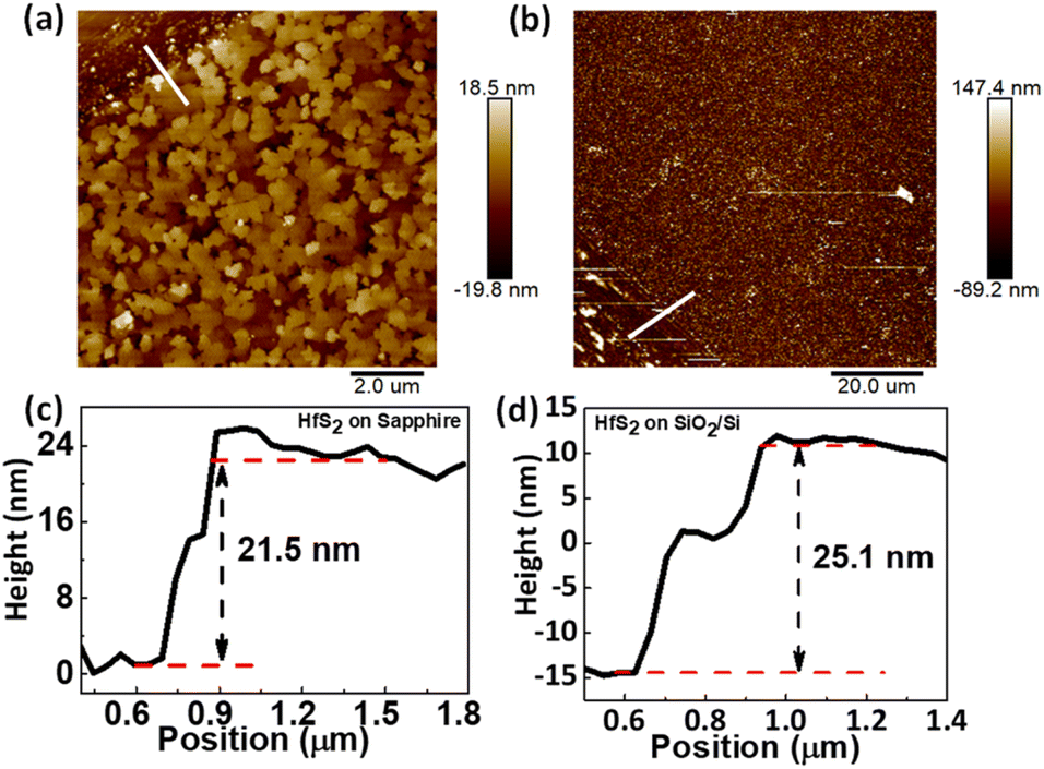 | ||
| Fig. 3 Atomic force microscopy (AFM) images of few layered HfS2 on (a) sapphire and (b) SiO2/Si substrates. (c) and (d) Height profiles of HfS2 on sapphire and SiO2/Si substrates, respectively. | ||
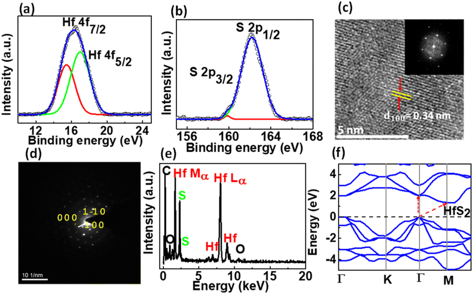 | ||
| Fig. 4 (a) and (b) X-ray photoemission spectroscopy (XPS) spectra of as-grown HfS2, (a) is the Hf 4f states allocated with two peaks, while (b) is the S 2p states, respectively. (c) High-resolution transmission microscopy (HR-TEM) image of HfS2. The inset shows the fast Fourier transform (FFT) image of HfS2. (d) Selected area electron diffraction (SAED) pattern from the selected area of the crystal. (e) The TEM energy dispersive X-ray spectroscopy (EDS) survey spectrum of HfS2 (f) The calculated band structure of hexagonal HfS2, the arrows inside show direct and indirect bandgaps between the valence and conduction bands of HfS2. | ||
To further characterize the structure of HfS2, high-resolution transmission electron microscopy (HR-TEM) images of few layered HfS2 were recorded using an HR-TEM setup. Fig. 4(c) shows the top-view HR-TEM image of HfS2 and indicates that the lattice fringe with 0.34 nm spacing corresponds to the (100) plane of HfS2. The inset shows the fast Fourier transform (FFT) of the lattice image. Fig. 4(d) displays the selective area electron diffraction (SAED) pattern of HfS2, showing hexagonal symmetry along with crystal plane distances of 3.06 Å and 3.05 Å which correspond to the (1![[1 with combining macron]](https://www.rsc.org/images/entities/char_0031_0304.gif) 0) and (100) planes of HfS2, respectively.
0) and (100) planes of HfS2, respectively.
The TEM energy dispersive X-ray spectroscopy (EDS) spectrum in Fig. 4(e) reveals the existence of both Hf and S elements. From this spectrum, the stoichiometry ratio is estimated and found to be very close to 1![[thin space (1/6-em)]](https://www.rsc.org/images/entities/char_2009.gif) :2, which indicates the stoichiometric composition of as-grown HfS2. To calculate the band structure, density of states, and optical properties of HfS2, density functional theory (DFT) calculations were performed. The calculated density of states of HfS2 is shown in Fig. S2(d),† while the band structure is shown in Fig. 4(f). The band structure of HfS2 reveals the direct (∼1.35 eV) and indirect bandgap (∼2 eV) between the maxima of the valence band and minima of the conduction band, respectively. Direct excitonic transitions occur between the Γ points while indirect transitions occur between the Γ and M points shown by the red arrow (Fig. 4(f)). Also, the thickness distribution of HfS2 layers broadens the absorption range.24 Thus, the strong absorption (Fig. 2(e)) due to the indirect and direct transition of charge carriers from the valence to the conduction band suggests the potential application of few-layered HfS2 for various optoelectronic devices.
:2, which indicates the stoichiometric composition of as-grown HfS2. To calculate the band structure, density of states, and optical properties of HfS2, density functional theory (DFT) calculations were performed. The calculated density of states of HfS2 is shown in Fig. S2(d),† while the band structure is shown in Fig. 4(f). The band structure of HfS2 reveals the direct (∼1.35 eV) and indirect bandgap (∼2 eV) between the maxima of the valence band and minima of the conduction band, respectively. Direct excitonic transitions occur between the Γ points while indirect transitions occur between the Γ and M points shown by the red arrow (Fig. 4(f)). Also, the thickness distribution of HfS2 layers broadens the absorption range.24 Thus, the strong absorption (Fig. 2(e)) due to the indirect and direct transition of charge carriers from the valence to the conduction band suggests the potential application of few-layered HfS2 for various optoelectronic devices.
To understand the optoelectronic properties of few-layered HfS2, a typical HfS2 photodetector on a sapphire substrate was fabricated. The schematic of the HfS2 photodetector is shown in Fig. 5(a). Briefly, Ni (50 nm) contacts were deposited on the top of HfS2 on a sapphire substrate using an interdigitated finger shadow mask (separated by a distance of 300 μm). Fig. 5(b) shows the typical current density–voltage (J–V) characteristics of the HfS2 photodetector in the bias voltage range of ±20 V under dark and green laser (532 nm) light illumination conditions as a function of laser power density. An ohmic contact was formed between the Ni electrode and HfS2 layer as represented by symmetrical log J–V characteristics. Under dark conditions, the photodetector reveals a current density of ∼5 nA cm−2 at an applied bias voltage of ±20 V, while under green laser light illumination, the current density increased by a factor of ∼10 at a power density of 9 mW cm−2.
 | ||
| Fig. 5 (a) Schematic diagram of the fabricated HfS2 photodetector. (b) Current–voltage (I–V) characteristics of the fabricated photodetector on c-plane sapphire under dark and under green (532 nm) laser light illumination conditions at different laser power densities. (c) The responsivity vs. bias voltage curve of the photodetector at different laser intensities. (d) The responsivity of the photodetector as a function of laser power densities at an applied bias voltage of 20 V. | ||
Further, with increasing the laser power density from 9 to 38 mW cm−2, the photocurrent increases, and it becomes saturated at a power density of 68 mW cm−2. The saturation of photocurrent with laser power density can be attributed to the trapping of generated electron–hole pairs by the available few trap states and defects in the interfacial region. At a high power density and applied bias of ±20 V, the active layer shows a poor density of generated charge carriers i.e. carriers could not get sufficient activation energy to overcome the built-in potential barrier in the interfacial region. Herein, the potential barrier is formed by a trap and defects due to the different work functions of the electrode and HfS2. Therefore, at high power density, the generation of free charge carriers can be limited due to the trapping of some carriers by trap and defect states as a result of the saturation of photocurrent. Furthermore, to evaluate the performance of the fabricated photodetector, the responsivity (R) is calculated under green laser light illumination as a function of bias voltage and laser power density as shown in Fig. 5(c) and (d), respectively, and can be defined as:
 | (2) |
The responsivity is measured at different laser power densities as a function of bias voltage and found to be ∼1.6, ∼0.38, and ∼0.21 μA W−1 corresponding to 9, 38, and 68 mW cm−2, respectively (Fig. 5(c)). The measured responsivity of ∼1.6 μA W−1 corresponding to 9 mW cm−2 is similar to the reported responsivity of ∼9.0 × 10⁻⁵ A W−1 of multilayer MoS2 phototransistor in near-infrared photo detection.38 Also, these responsivity values are highly comparable to the reported responsivity of ∼10−2 mA W−1 for the photodetector based on epitaxially grown HfS2 on a sapphire substrate.18 However, the values are lower than the reported responsivity of ∼890 A W−1 for the HfS2 phototransistor based on the exfoliation method.11 Herein, the lower responsivity can be associated with the higher resistivity of HfS2 layers. Fig. 5(d) represents the variation of responsivity as a function of laser power density. It is noticed that with increasing the laser power density, the responsivity gradually decreases and this is attributed to the change in the photon intensity upon light illumination. Further, we have also investigated the photoresponse and responsivity of the HfS2 photodetector as a function of bias voltage and laser power density under UV (342 nm) laser and white light illumination conditions as shown in Fig. S3(a–c) and (d–f),† respectively. The photodetector exhibits a similar kind of photoresponse to that reported under green laser light illumination. A comparison of all the photo-responsivities was demonstrated under different laser light illumination conditions and plotted as a function of laser power density as shown in Fig. S4.† It was noticed that no significant change in the responsivities was observed i.e. the responsivities remain almost the same (except for smaller variation) under all laser light illumination conditions. This can be associated with the fact that the rate of generation of electron–hole pairs i.e. excitons, remains independent of the type (i.e. UV to visible region) of laser light illumination.
To further evaluate the temporal response of the fabricated HfS2 photodetector, the current–time (I–t) measurements were performed under green laser light illumination (532 nm, @power density 38 mW cm−2) in ON/OFF switching mode at an applied bias voltage of 1 V as shown in Fig. 6(a). The results distinctly reveal that the HfS2 photodetector shows good repeatability over many cycles as evident from ON/OFF cycles of the I–t curve and the ON/OFF ratio was found to be <10. By considering one cycle of the I–t curve, the rise time and fall time between peak saturation values from 10% to 90% and 90% to 10% were estimated and found to be ∼0.33 and ∼0.40 seconds, respectively. Herein, the values of rise and fall times are found to be a little higher compared to the reported values of rise and fall times of ∼24 ms of the photodetector based on vertically orientated few-layered HfS2 nanosheets.24 The higher values of rise and fall can be ascribed to the high resistance at the interface of the device. This adequately affects the electron–hole separation at the interface and leads to the deterioration of the prompt charge carrier transport in the active region of the photodetector. This can also be attributed to the defect induced recombination of generated charge carriers before transporting them to their respective electrodes. Future work will be focused on optimizing and design architecture processing of the device, which will substantially enhance the performance of our HfS2 photodetector for various advanced optoelectronic devices.
 | ||
| Fig. 6 (a) Current–time (I–t) curve of the fabricated HfS2 photodetector under periodically turning ON/OFF of a green laser light at an applied bias voltage of 1 V. (b) and (c) are the typical rise and fall times calculated from one single photoresponse cycle of (a). | ||
Furthermore, to investigate the electronic properties of HfS2, we fabricated field effect transistors (FETs) based on directly grown HfS2 on SiO2/Si using Au (95 nm)/Ni (5 nm) as a source and drain electrode and SiO2 as a dielectric with p+-type Si as a back gate electrode. The schematic of the FET device is shown in Fig. 7(a). Detailed information about the fabrication of FETs is available in the experimental section. Fig. 7(b) shows the Id–Vg curve at Vd = 5 V with Vg from −10 V to +10 V. The transfer characteristics of the few-layered HfS2 FET were measured at room temperature and reveal p-type behaviour with an on/off ratio of ∼103, which is lower compared to that of the n-type device. To the best of our knowledge, several studies have been reported on the transfer of HfS2 from sapphire to the SiO2/Si substrate. However, herein for the first time, we directly grew HfS2 on SiO2/Si and report its FET characteristics. We have observed a lower on/off ratio in our case compared to other reported on/off responses which can be attributed to the formation of defects, wrinkles, and charge trapping at the interface during the growth process. To confirm the p-type behaviour of our FET device, the Id–Vd characteristics were also measured at 0 V and a negative back gate bias voltage of −2 V with a sweeping voltage of −3.5 V to +3.5 V as shown in the inset of Fig. 7(b). Initially, at 0 V gate bias voltage, the forward and reverse currents are observed as ∼0.035 and ∼−0.028 μA, respectively. As we applied a negative gate bias voltage of −2 V, the forward and reverse current increased as a result of the p-type behaviour of the device. The p-type behaviour of our device can be associated with the increase in the charge trapping at the interface with applied negative gate bias voltage. Thus, the combination of very good responsivity, fast response time, and p-type conduction of HfS2 makes it a favourable layered material for potential photodetector and FET devices.
 | ||
| Fig. 7 Electrical measurements of the directly fabricated back gate HfS2 FET device on the SiO2/Si substrate. (a) Schematic of the fabricated back gate HfS2 FET device. (b) Id–Vg output characteristics of the back gate FET device at an applied drain bias voltage of 5 V. The inset shows the Id–Vg characteristics of the back gate FET device at an applied back gate bias voltage of 0 V and −2 V. | ||
4. Conclusion
The successful growth of few-layered hafnium disulfide (HfS2) on c-plane sapphire as well as directly on SiO2/Si substrates has been demonstrated using CVD. The structural properties were measured by recording the Raman and XRD spectra of HfS2 grown on sapphire and directly on the SiO2/Si substrate, which exhibit the high crystalline quality of HfS2 on both types of substrates. The optical properties of as-grown HfS2 were investigated and well matched with the theoretical results. The optical bandgap from the absorption spectra of HfS2 was estimated using the Tauc plot and found to be ∼2.59 eV (indirect bandgap). DFT calculations were performed to calculate the optical properties, band structure, and density of states. Furthermore, the photodetector was fabricated based on as-grown HfS2 on sapphire and demonstrates excellent UV to visible light sensing performance with an ON/OFF ratio of about 10. The rise and recovery times were estimated and found to be ∼0.33 and ∼0.40 seconds under green laser light illumination. Moreover, a back gate FET based on few-layered HfS2 directly grown on SiO2/Si was fabricated, and it exhibits p-type behaviour. Thus, herein we for the first time report the growth mechanism of transfer-free directly grown HfS2 on SiO2/Si which can become a promising method to synthesize high quality 2D few layers on different substrates for potential cutting-edge electronic and optoelectronic devices.Conflicts of interest
There are no conflicts to declare.Acknowledgements
This study was supported in parts by the Ministry of Science and Technology (MOST) of Taiwan under 107-2218-E-011-023-MY3 and 109-2622-E-011-011-CC3.References
- Y. Liu, R. Cheng, L. Liao, H. Zhou, J. Bai, G. Liu, L. Liu, Y. Huang and X. Duan, Nat. Commun., 2011, 2, 1–7 Search PubMed
.
- K. S. Novoselov, A. K. Geim, S. V Morozov, D. Jiang, Y. Zhang, S. V Dubonos, I. V Grigorieva and A. A. Firsov, Science, 2004, 306, 666–669 CrossRef CAS
- A. Hashimoto, K. Suenaga, A. Gloter, K. Urita and S. Iijima, Nature, 2004, 430, 870–873 CrossRef CAS
- K. S. Novoselov, A. Mishchenko, A. Carvalho and A. H. Castro Neto, Science, 2016, 353(6298), aac9439 CrossRef CAS PubMed
- L. M. Xie, Nanoscale, 2015, 7, 18392–18401 RSC
- D.-H. Lien, J. S. Kang, M. Amani, K. Chen, M. Tosun, H.-P. Wang, T. Roy, M. S. Eggleston, M. C. Wu and M. Dubey, Nano Lett., 2015, 15, 1356–1361 CrossRef CAS
- Y. Lee, X. Zhang, W. Zhang, M. Chang, C. Lin, K. Chang, Y. Yu, J. T. Wang, C. Chang and L. Li, Adv. Mater., 2012, 24, 2320–2325 CrossRef CAS PubMed
- S. Larentis, B. Fallahazad and E. Tutuc, Appl. Phys. Lett., 2012, 101, 223104 CrossRef
- L. Britnell, R. M. Ribeiro, A. Eckmann, R. Jalil, B. D. Belle, A. Mishchenko, Y.-J. Kim, R. V Gorbachev, T. Georgiou and S. V Morozov, Science, 2013, 340, 1311–1314 CrossRef CAS PubMed
- A. K. Geim and I. V Grigorieva, Nature, 2013, 499, 419–425 CrossRef CAS PubMed
- K. Xu, Z. Wang, F. Wang, Y. Huang, F. Wang, L. Yin, C. Jiang and J. He, Adv. Mater., 2015, 27, 7881–7887 CrossRef CAS PubMed
- K. Xu, Y. Huang, B. Chen, Y. Xia, W. Lei, Z. Wang, Q. Wang, F. Wang, L. Yin and J. He, Small, 2016, 12, 3106–3111 CrossRef CAS PubMed
- R. Yue, A. T. Barton, H. Zhu, A. Azcatl, L. F. Pena, J. Wang, X. Peng, N. Lu, L. Cheng and R. Addou, ACS Nano, 2015, 9, 474–480 CrossRef CAS
- L. Li, X. Fang, T. Zhai, M. Liao, U. K. Gautam, X. Wu, Y. Koide, Y. Bando and D. Golberg, Adv. Mater., 2010, 22, 4151–4156 CrossRef CAS
- C. Gong, H. Zhang, W. Wang, L. Colombo, R. M. Wallace and K. Cho, Appl. Phys. Lett., 2013, 103, 53513 CrossRef
- W. Zhang, Z. Huang, W. Zhang and Y. Li, Nano Res., 2014, 7, 1731–1737 CrossRef CAS
- G. Fiori, F. Bonaccorso, G. Iannaccone, T. Palacios, D. Neumaier, A. Seabaugh, S. K. Banerjee and L. Colombo, Nat. Nanotechnol., 2014, 9, 768–779 CrossRef CAS PubMed
- D. Wang, X. Zhang, H. Liu, J. Meng, J. Xia, Z. Yin, Y. Wang, J. You and X.-M. Meng, 2D Mater., 2017, 4, 31012 CrossRef
- C. Yan, L. Gan, X. Zhou, J. Guo, W. Huang, J. Huang, B. Jin, J. Xiong, T. Zhai and Y. Li, Adv. Funct. Mater., 2017, 27, 1702918 CrossRef
- D. Dumcenco, D. Ovchinnikov, K. Marinov, P. Lazic, M. Gibertini, N. Marzari, O. L. Sanchez, Y.-C. Kung, D. Krasnozhon and M.-W. Chen, ACS Nano, 2015, 9, 4611–4620 CrossRef CAS PubMed
- S. Tongay, W. Fan, J. Kang, J. Park, U. Koldemir, J. Suh, D. S. Narang, K. Liu, J. Ji and J. Li, Nano Lett., 2014, 14, 3185–3190 CrossRef CAS
- X. Wang, L. Huang, X.-W. Jiang, Y. Li, Z. Wei and J. Li, J. Mater. Chem. C, 2016, 4, 3143–3148 RSC
- S. H. Chae, Y. Jin, T. S. Kim, D. S. Chung, H. Na, H. Nam, H. Kim, D. J. Perello, H. Y. Jeong and T. H. Ly, ACS Nano, 2016, 10, 1309–1316 CrossRef CAS PubMed
- B. Zheng, Y. Chen, Z. Wang, F. Qi, Z. Huang, X. Hao, P. Li, W. Zhang and Y. Li, 2D Mater., 2016, 3, 35024 CrossRef
- J. Xia, X. Huang, L.-Z. Liu, M. Wang, L. Wang, B. Huang, D.-D. Zhu, J.-J. Li, C.-Z. Gu and X.-M. Meng, Nanoscale, 2014, 6, 8949–8955 RSC
- Y.-H. Lee, L. Yu, H. Wang, W. Fang, X. Ling, Y. Shi, C.-T. Lin, J.-K. Huang, M.-T. Chang and C.-S. Chang, Nano Lett., 2013, 13, 1852–1857 CrossRef CAS
- B. Zheng, Z. Wang, F. Qi, X. Wang, B. Yu, W. Zhang and Y. Chen, Appl. Surf. Sci., 2018, 435, 563–567 CrossRef CAS
- S. J. Clark, M. D. Segall, C. J. Pickard, P. J. Hasnip, M. I. J. Probert, K. Refson and M. C. Payne, Z. fur Krist.–Cryst. Mater., 2005, 220, 567–570 CrossRef CAS
- J. P. Perdew, Phys. Rev. Lett., 1996, 77, 3865 CrossRef CAS PubMed
- L. E. Conroy and K. C. Park, Inorg. Chem., 1968, 7, 459–463 CrossRef CAS
- X. Zhang, X.-F. Qiao, W. Shi, J.-B. Wu, D.-S. Jiang and P.-H. Tan, Chem. Soc. Rev., 2015, 44, 2757–2785 RSC
- X. Zhang, Q.-H. Tan, J.-B. Wu, W. Shi and P.-H. Tan, Nanoscale, 2016, 8, 6435–6450 RSC
- M. Traving, T. Seydel, L. Kipp, M. Skibowski, F. Starrost, E. E. Krasovskii, A. Perlov and W. Schattke, Phys. Rev. B: Condens. Matter Mater. Phys., 2001, 63, 35107 CrossRef
- D. L. Greenaway and R. Nitsche, J. Phys. Chem. Solids, 1965, 26, 1445–1458 CrossRef CAS
- K. Terashima and I. Imai, Solid State Commun., 1987, 63, 315–318 CrossRef CAS
- K. F. Mak, C. Lee, J. Hone, J. Shan and T. F. Heinz, Phys. Rev. Lett., 2010, 105, 136805 CrossRef PubMed
-
Handbook of X-Ray Photoelectron Spectroscopy: A Reference Book of Standard Spectra for Identification and Interpretation of XPS Data, ed. J. F. Moulder, J. Chastain and R. C. King, Physical Electronics Division, Perkin–Elmer Corp., Eden Prairie, Minnesota, 1995 Search PubMed
- W. Choi, M. Y. Cho, A. Konar, J. H. Lee, G. Cha, S. C. Hong, S. Kim, J. Kim, D. Jena and J. Joo, Adv. Mater., 2012, 24, 5832–5836 CrossRef CAS PubMed
Footnote |
| † Electronic supplementary information (ESI) available. See DOI: https://doi.org/10.1039/d2na00578f |
| This journal is © The Royal Society of Chemistry 2023 |