
 Open Access Article
 This Open Access Article is licensed under a Creative Commons Attribution-Non Commercial 3.0 Unported Licence
Tunable resonance of a graphene-perovskite terahertz metasurface
Guibin
Li
a,
Guocui
Wang
ab,
Yan
Zhang
 a,
Jingling
Shen
a and
Bo
Zhang
*a
a,
Jingling
Shen
a and
Bo
Zhang
*a
aKey Laboratory of Terahertz Optoelectronics, Ministry of Education, Advanced Innovation Center for Imaging Technology, Beijing Key Laboratory for Terahertz Spectroscopy and Imaging, Beijing Key Laboratory of Metamaterials and Devices, Department of Physics, Capital Normal University, Beijing, 100048, China. E-mail: bzhang@cnu.edu.cn
bBeijing Engineering Research Center for Mixed Reality and Advanced Display, School of Optics and Photonics, Beijing Institute of Technology, Beijing 100081, China
First published on 9th January 2023
Abstract
The combination of graphene and perovskite has received extensive research attention because its photoelectric properties are excellent for the dynamic manipulation of light–matter interactions. Combining graphene and perovskite with a metasurface is expected to effectively improve the metasurface device's performance. Here, we report a terahertz graphene-perovskite metasurface with a tunable resonance. Under 780 nm laser excitation, the device's THz transmission is significantly reduced, and the Fano resonance mode can be manipulated in multiple dimensions. We verify the experimental results using a finite-difference time-domain (FDTD) simulation. Graphene and perovskite interact strongly with the metasurface, resulting in a short-circuit effect, which significantly weakens the resonance intensity of the Fano mode. The photoinduced conductivity enhancement intensifies the short-circuit effect, reducing the THz transmission and resonance intensity of the Fano mode and causing the resonance frequency to redshift. Finally, we provide a reference value for applications of hybrid metasurface-based optical devices in a real environment by investigating the effect of moisture on device performance.
1. Introduction
Metasurfaces are a cluster of two-dimensional artificial materials comprising an inerratic array of periodical, metal or dielectric, sub-wavelength structures. They have attracted extensive attention as a new way to manipulate electromagnetic waves for diverse applications, including as absorbers,1–3 modulators,4–6 and biosensors7–10 because of their unusual optical properties, including negative refractive indices, superlensing, artificial magnetism, and hyperbolic dispersion.11–17 Their major mechanism is the sensitivity of their resonance modes to changes in the microenvironment. However, when the material and structural parameters of a metasurface are fixed, the resonance modes become stable, greatly limiting the metasurface's potential applications. Therefore, the combination of metasurfaces with other semiconductor materials provides new opportunities and possibilities for the development of dynamic, functional THz devices.18–21Perovskite is a material with the structure ABX3, where A is an organic or inorganic cation, B is a metal cation, and X is a halide anion. Perovskite materials can be divided into inorganic metallic halide perovskites (A = Cs; B = Pb, Sn; X = Cl, Br, I) and organometallic halide perovskites (A = CH3NH3, CH3CH2NH3; B = Pb, Sn; X = Cl, Br, I). In recent years, organometallic halide perovskites have shown excellent performance in solar cells, photodetectors, and other optoelectronic devices. They have attracted great research attention because of their tunable optical band gap, high light absorption coefficients, high carrier mobility, low cost, long carrier diffusion distance, low-temperature processing, extremely low exciton binding energy, and efficient charge transportation to the selective contact layers.22–29
To further improve device performance, it is necessary to combine organometallic halide perovskites with other semiconducting materials such as graphene. Graphene is a single-atom-thick planar sheet of sp2-hybridized carbon in a honeycomb lattice. Novoselov et al. first successfully synthesized monolayer graphene from bulk graphite in 2004 using mechanical exfoliation.30 Research into the material's properties began with its magnetotransport properties and anomalous Berry phase,31,32 and its optical, electronic, mechanical, and thermal properties have attracted much attention since. Monolayer graphene possesses high carrier mobility, zero band-gap, tunable optical absorption, strong terahertz response, optical transparency, mechanical flexibility, high Fermi velocity, a tunable Fermi level, and many other unique properties.33–41 Monolayer graphene, as a two-dimensional semiconductor material, can be combined with perovskite to form a hybrid structure, which is a promising route to effectively controlling light–matter interactions and improving metasurface device performance.42–44
Here, we propose an actively tunable hybrid terahertz metasurface device comprising monolayer graphene and organometallic halide perovskite (CH3NH3PbI3). Without photoexcitation, the metasurface device has two weak resonance peaks. The one at a lower frequency is the Fano resonance mode, and the one at a higher frequency is the dipole resonance mode. When 780 nm laser excitation at 250 mW cm−2 is applied to the device, the THz transmission is significantly reduced. Because of the two modes' different physical mechanisms, the Fano resonance mode is the more sensitive to photoexcitation, and its resonance intensity is reduced while the frequency is significantly redshifted. To explain these observations, we calculated the device conductivity using equivalent transmission line theory and established an equivalent circuit model. We also verified the experimental results using a finite-difference time-domain (FDTD) simulation. Finally, we simulate the effect of a humid environment on device performance by spraying a layer of water mist uniformly on the surface of the device.
2. Experimental details
The experimental measurement system is a THz time-domain spectroscopic (THz-TDS) system, as shown in Fig. 1(a). The enlarged view in Fig. 1(a) shows the overall structure of the sample and its components. Monolayer graphene was prepared by chemical vapor deposition and shifted to an undefiled quartz substrate with the dimensions 2 cm × 2 cm × 1 mm. Fig. 1(b) shows the Raman spectrum of the graphene on the quartz substrate. The locations of the G peak at ∼1586 cm−1 and the 2D peak at ∼2672 cm−1 demonstrate the high quality of the monolayer graphene.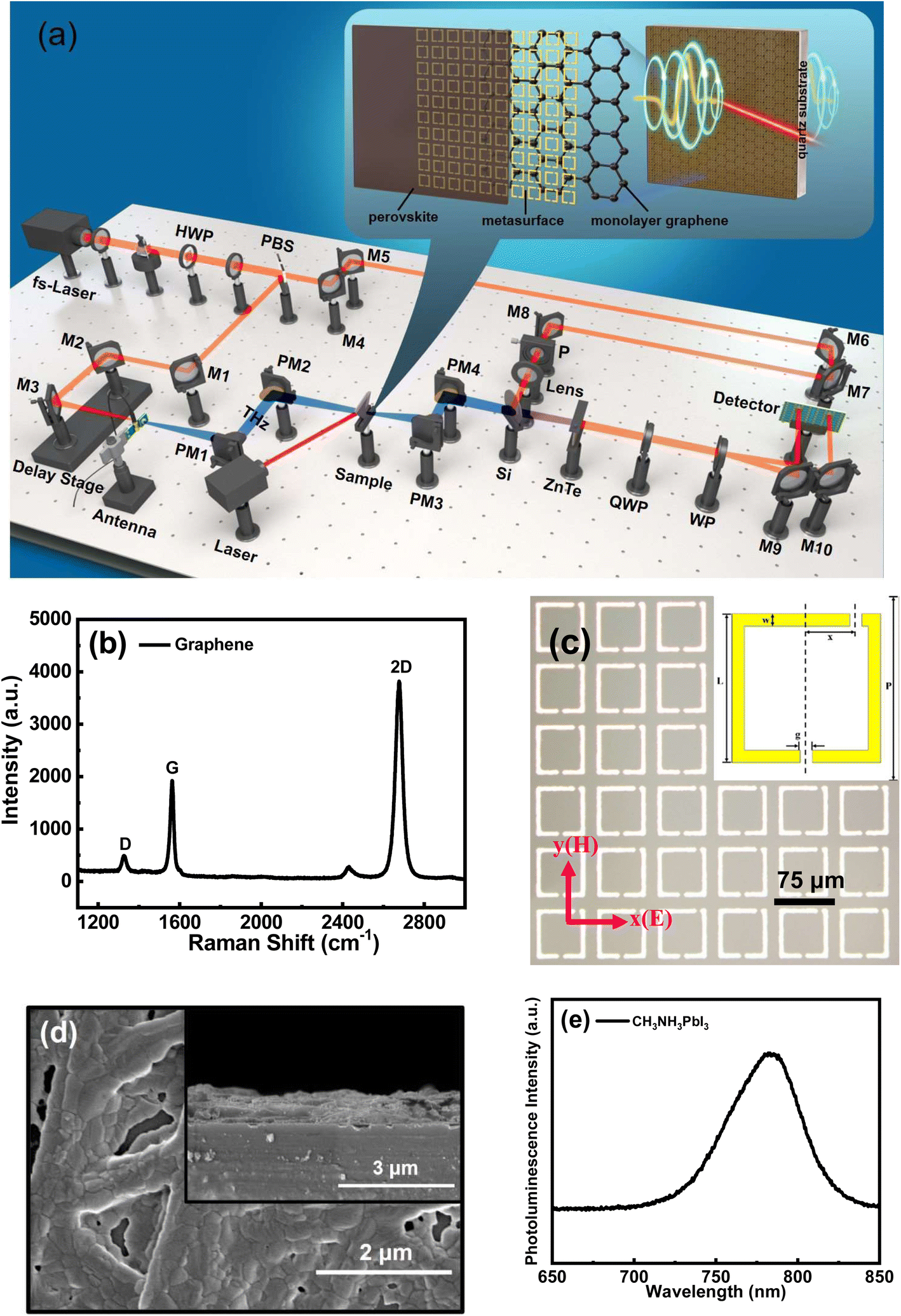 | ||
| Fig. 1 (a) Schematic of the terahertz time-domain spectroscopic system and the sample used in this study. (b) Raman spectrum of monolayer graphene on a quartz substrate. (c) Microscope image of the terahertz asymmetric split-ring resonator. The inset shows the structural parameters of the unit cell. Scale bar = 75 μm. (d) SEM surface and cross-sectional images of the CH3NH3PbI3/TASR/graphene/quartz device. (e) A photoluminescence image of the CH3NH3PbI3. | ||
The metasurface was fabricated on the monolayer graphene sheet via ultraviolet lithography. A microscope image of the metasurface is shown in Fig. 1(c), where the structure and parameters of the unit cell are shown in the inset. The unit cell of the metasurface is a terahertz asymmetric split-ring resonator (TASR). The configurable parameters of the TASR are as follows: outer length L = 60 μm, line width w = 5 μm, gap width (function as an equivalent capacitor) g = 5 μm, and period P = 75 μm. One of the gaps is aligned with the center of the unit cell, while the other is displaced from the center by x = 20 μm to create the asymmetry of the structure. The structural asymmetry of the resonator is why the sharp, dark Fano resonance mode is excited.
Finally, the perovskite (CH3NH3PbI3) solution was obtained by putting 200 mg of methyl ammonium iodide (CH3NH3I) and 600 mg of PbI2 into a reagent bottle, followed by adding 1 ml of dimethylformamide, and sonication at 70 °C for 30 min. A proper amount of the prepared perovskite solution was taken and dropped on the TASR/graphene/quartz sample. The spinning coating speed was set as 1000 rpm for the first 15 s and 2000 rpm for the last 30 s. Chlorobenzene solution was dropped at the 8th second of the spin-coating process to induce crystallization, and then the film was formed. Finally, the spin-coated sample was annealed at 100 °C for 15 min. Scanning electron microscopy (SEM) images of the surface and cross section of the CH3NH3PbI3/TASR/graphene/quartz sample are shown in Fig. 1(d). The photoluminescence of the CH3NH3PbI3 was measured, as shown in Fig. 1(e).
3. Results and discussion
Fig. 2(a) and (b) show the frequency-domain THz transmission signals of the TASR/quartz and TASR/graphene/quartz samples, respectively. In the absence of graphene, we observe two distinct resonant absorption minima at 778 and 1172 GHz. The sharp resonant absorption at the lower frequency corresponds to the Fano resonant mode, which has a high Q factor. The resonance absorption at the higher frequency corresponding to the dipole resonant mode, which has a higher intensity and broad line width. After adding the monolayer graphene, the resonant intensities of both modes are significantly decreased, and the frequency of the Fano mode shows an obvious redshift, while that of the dipole resonance mode undergoes a blueshift.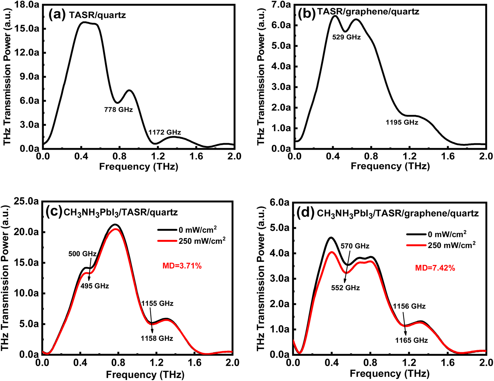 | ||
| Fig. 2 Frequency-domain THz transmission signals of (a) the TASR/quartz device and (b) the TASR/graphene/quartz device without photoexcitation. (c, d) Frequency-domain THz transmission signals of (c) the CH3NH3PbI3/TASR/quartz device and (d) the CH3NH3PbI3/TASR/graphene/quartz device without (black) and with (red) photoexcitation at 780 nm with a continuous-wave laser at 250 mW cm−2. | ||
Fig. 2(c) and (d) show the frequency-domain THz transmission signals of the CH3NH3PbI3/TASR/quartz and CH3NH3PbI3/TASR/graphene/quartz samples without and with photoexcitation by a 780 nm laser at 250 mW cm−2. Without photoexcitation, the CH3NH3PbI3/TASR/quartz sample has two weak resonances at 500 and 1155 GHz, corresponding to the Fano and dipole resonance modes, respectively. 780 nm laser excitation causes the THz transmission to decrease slightly, the frequency of the Fano resonance to weakly redshift from 500 GHz to 495 GHz, and the frequency of the dipole resonance to faintly blueshift from 1155 GHz to 1158 GHz, while the resonance intensity of the two modes barely changes.
In contrast, the response of the CH3NH3PbI3/TASR/graphene/quartz sample is greatly amplified. There are two weak resonances at 570 GHz and 1156 GHz, corresponding to the Fano and dipole modes. When the sample is excited at 780 nm, the THz transmission decreases significantly, while the Fano and dipole resonances undergo more significant red- and blueshifts, from 570 GHz to 552 GHz and from 1156 GHz to 1165 GHz, respectively. It is worth noting that the intensity of the Fano resonance is obviously weakened during this process, while that of the dipole resonance is almost unchanged.
To quantify the THz modulation, a modulation depth (MD) is defined as follows:45–49
 | (1) |
The lower-frequency Fano resonance mode of the metamaterial can only be excited because the inherent symmetry of the split-ring structure is broken by the displacement of one of the its gaps from the center of the unit cell (see Fig. 1(c)). The Fano resonance is a dark-mode resonance, weakly coupled to free space and excited by sub-radiant, anti-parallel surface currents in the asymmetric resonator, so it is a sharp resonance with high Q factor and low radiative losses.50–52 The resonance at higher frequency, the dipole resonance mode, is excited by a dipole-like parallel surface current in the split-ring resonator. The dipole resonance is almost independent of the unit cell symmetry and exists in both asymmetric and symmetric split-ring resonator structures. The dipole resonance is a bright mode resonance with intense radiation coupling to free space, broad resonant line width, and high resonant intensity.53
After adding graphene and/or perovskite, both the Fano and dipole resonance modes change significantly. The metasurface creates a strong electric field in the two capacitance gaps of the asymmetric resonator by confining the electric field to a high sub-wavelength volume, increasing the interaction intensity between the field and the material layers. Because of this, both resonance modes are affected by the addition of graphene and/or perovskite.
We used an equivalent circuit model to further interpret the mechanism of the interaction between the metasurface and the material layer.54–57 The metallic stripes of the resonator correspond to the inductances (L1 and L2), the split gaps correspond to the capacitances (C1 and C2), and dissipation corresponds to the resistances (R1 and R2). Fig. 3(a) shows the equivalent circuit of the TASR/quartz sample. Considerable charge accumulates at both ends of the two gaps in the asymmetric resonator—equivalently, the plates of the two capacitors—resulting in an intense electric field in the resonator gaps. This corresponds to the sharp Fano resonant mode with high Q factor and a dipole resonant mode with broad line width and high intensity. The addition of monolayer graphene and perovskite is equivalent to adding parallel resistances Rg and Rp (functioning as an equivalent resistance Re) at both ends of each equivalent capacitance, as shown in Fig. 3(b). This induces a short-circuit effect, significantly suppressing the electric field in the two gaps of the asymmetric resonator and decreasing the electric field strength, therefore reducing the intensities of both resonance modes.
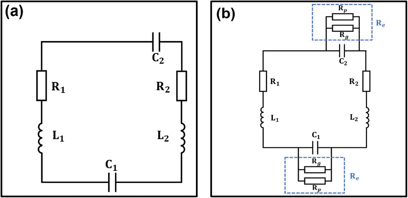 | ||
| Fig. 3 Equivalent circuit models of (a) the TASR/quartz device and (b) the CH3NH3PbI3/TASR/graphene/quartz device. | ||
For the CH3NH3PbI3/TASR/graphene/quartz sample, the THz transmission decreases significantly upon photoexcitation, while for the CH3NH3PbI3/TASR/quartz sample, the THz transmission decreases only slightly. To explain this, we used equivalent transmission line theory to calculate the change in sample conductivity.58,59 The complex transmission function of a conductive film can be denoted as
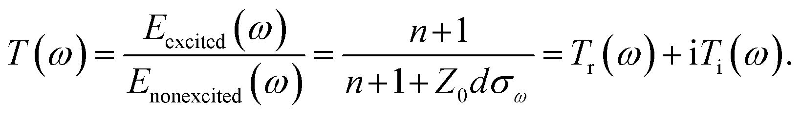 | (2) |
The real and imaginary parts of the film conductivity are then:
 | (3) |
 | (4) |
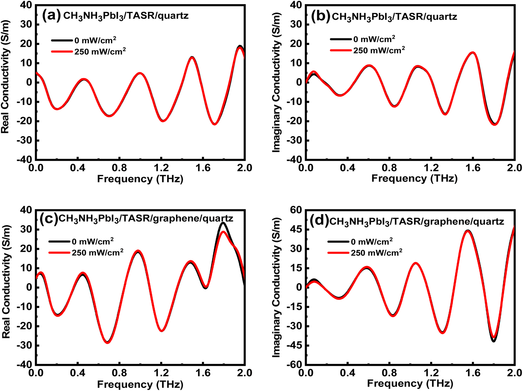 | ||
| Fig. 4 The (a) real and (b) imaginary parts of the conductivity of the CH3NH3PbI3/TASR/quartz sample calculated using equivalent transmission line theory without (black) or with (red) photoexcitation by a 780 nm laser at 250 mW cm−2. The (c) real and (d) imaginary parts of the conductivity of the CH3NH3PbI3/TASR/graphene/quartz sample calculated using equivalent transmission line theory without (black) or with (red) photoexcitation. | ||
The real and imaginary conductivities of the CH3NH3PbI3/TASR/quartz sample are shown in Fig. 4(a) and (b). Both increase weakly under photoexcitation. The real and imaginary conductivities of the CH3NH3PbI3/TASR/graphene/quartz sample, shown in Fig. 4(c) and (d), show a more obvious increase compared with the CH3NH3PbI3/TASR/quartz sample. Under photoexcitation, the more the conductivity of the sample increases, the greater the modulation depth of the THz wave.
This can be explained by the way the graphene was prepared. Because the monolayer graphene was fabricated by chemical vapor deposition, it exhibits weak p-type doping.60 Therefore, under photoexcitation, a large number of photo-generated electron–hole pairs are generated in the CH3NH3PbI3 layer, and the electrons are transferred to the graphene layer, where they accumulate continuously, effectively reducing the recombination of carriers. In pure CH3NH3PbI3, electron–hole pairs generated under photoexcitation recombine rapidly. Therefore, compared with the CH3NH3PbI3/TASRs/quartz sample, the CH3NH3PbI3/TASRs/graphene/quartz sample has a more obvious increase in conductivity and more significant modulation of the THz transmission.
Under photoexcitation, the intensity of the Fano resonance mode of the CH3NH3PbI3/TASR/graphene/quartz sample also decreases, except the significant decrease in THz transmission, and the resonance frequency undergoes a significant redshift. The intensity of the dipole resonant mode barely changes, while its resonant frequency shows a blueshift. Thus, in the equivalent circuit model of the CH3NH3PbI3/TASR/graphene/quartz sample, the resistance Re in parallel with the equivalent capacity C decreases. As Re decreases, the inhibitory effect of the monolayer graphene and perovskite on the electric field in the gap increases, enhancing the short-circuit effect.
In the Fano resonance mode, there is a large amount of heterogeneous charge accumulation at both ends of the gaps in the asymmetric resonator, while for the dipole resonance mode, which has a different physical mechanism, the charge accumulation at the ends of the gaps is homogeneous. Therefore, the Fano resonance mode is more sensitive to the short-circuit effect; correspondingly, the resonance intensity of the Fano mode is weakened under photoexcitation, while that of the dipole mode is barely affected. Similarly, when a large number of photo-generated electron–hole pairs are generated in the sample under photoexcitation, the resonance frequency of the Fano mode shifts more obviously than that of the dipole mode.
To prove the reliability of these experiment results, we simulated the devices with a finite-difference time-domain (FDTD) solver. Fig. 5(a) shows the simulated frequency-domain signal of the TASR/quartz sample. In the absence of graphene and perovskite, there is a sharp resonance peak with high Q factor at 778 GHz, which is the dark Fano resonance mode, and a high-intensity resonance peak with broad linewidth at 1205 GHz, which is the bright dipole resonance mode. Fig. 5(b) shows the simulated frequency-domain signal of the CH3NH3PbI3/TASR/graphene/quartz sample, where we assume that the graphene and perovskite have the same conductivity. The conductivities of the graphene and perovskite in the simulation are set to a value equivalent to that obtained when applying continuous photoexcitation in the experiment. When the conductivities of the graphene and perovskite are 0 S m−1, there is a sharp, dark Fano resonance peak with high Q factor at 580 GHz, and a bright dipole resonant peak with broad line width and high intensity at 907 GHz. The addition of the graphene and perovskite results in a significant redshift of the frequencies of both the Fano and dipole resonance modes.
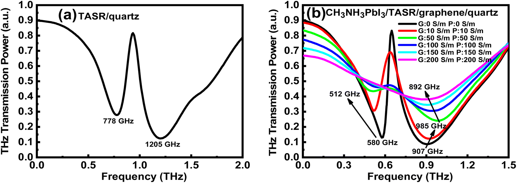 | ||
| Fig. 5 Simulations of the frequency-domain THz transmission of (a) the TASR/quartz sample or (b) the CH3NH3PbI3/TASR/graphene/quartz sample with varying graphene and perovskite conductivities. | ||
When the conductivities of the graphene and perovskite are increased to 50 S m−1, the resonance intensity of the Fano mode is significantly reduced, and its resonant frequency shows a redshift from 580 to 512 GHz. The intensity of the dipole resonant mode is also reduced gradually, and its resonant frequency shows a blueshift from 907 to 985 GHz. As the conductivities of the graphene and perovskite continue to increase, the Fano resonant mode disappears gradually, and only the dipole resonant mode remains, redshifted from 985 to 892 GHz. Therefore, consistent with the experimental results, it is mainly the Fano resonance that is affected by increasing the conductivities of the graphene and perovskite, while the dipole resonance mode is less affected.
Next, we simulated the electric field distributions under different conditions. Fig. 6(a) and (b) show the electric field distributions of the dark Fano resonance mode and the bright dipole resonance mode, respectively, of the TASR/quartz sample. In the absence of graphene and perovskite, there is a very intense electric field in the resonators in both the Fano and dipole modes, which corresponding to a sharp Fano resonant absorption with high Q factor and a dipole resonant absorption with broad line width and high intensity.
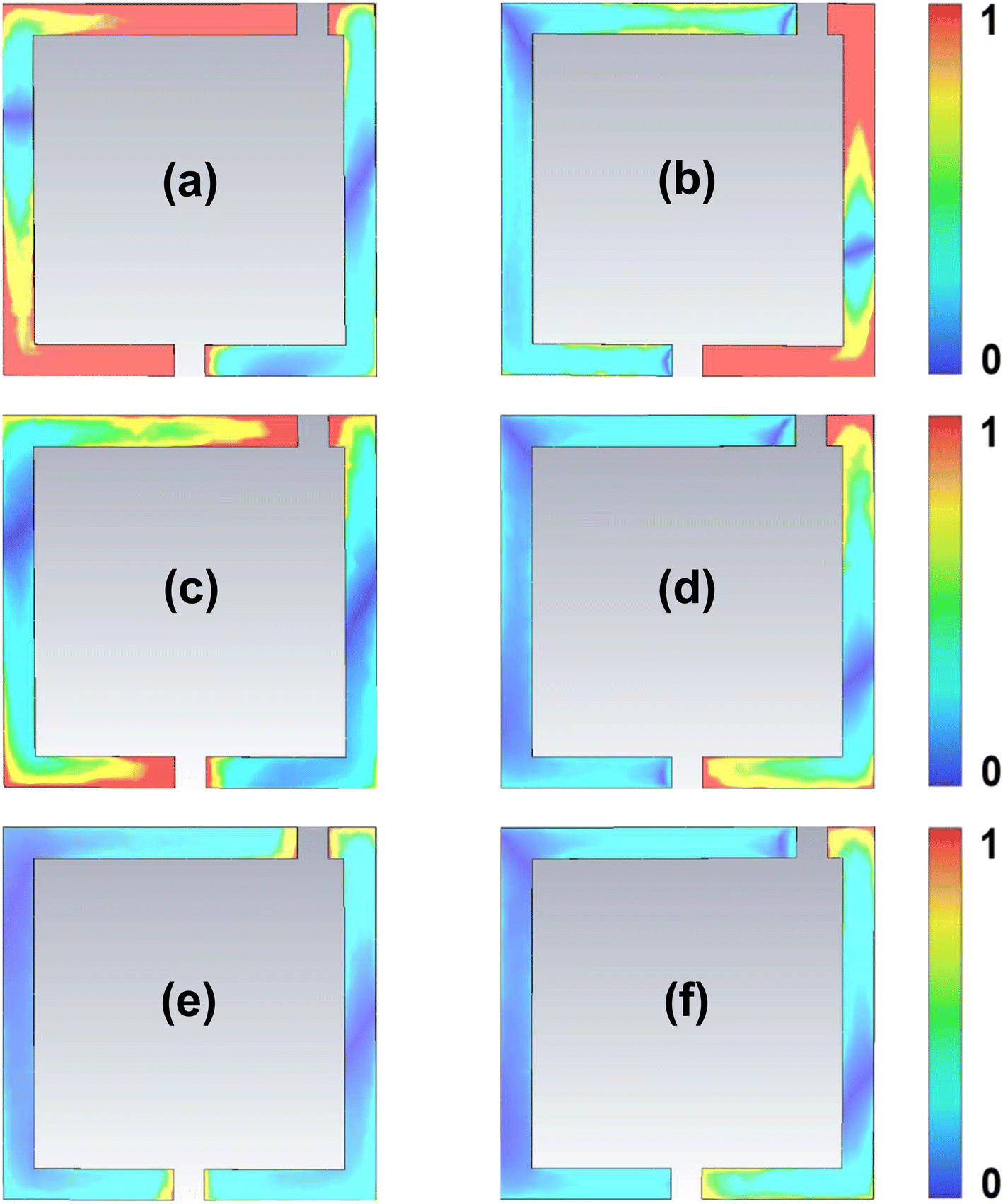 | ||
| Fig. 6 The electric field distributions of (a) the Fano resonance mode and (b) the dipole resonance mode of the TASR/quartz samples. (c, d) The electric field distributions of (c) the Fano resonance mode and (d) the dipole resonance mode of the CH3NH3PbI3/TASR/graphene/quartz samples with graphene and perovskite conductivity 10 S m−1. (e, f) The electric field distributions of (e) the Fano resonance mode and (f) the dipole resonance mode of the CH3NH3PbI3/TASR/graphene/quartz sample with graphene and perovskite conductivity 100 S m−1. | ||
Fig. 6(c) and (d) show the electric field distributions of the Fano and dipole resonance modes, respectively, of the CH3NH3PbI3/TASR/graphene/quartz samples when the conductivity of the graphene and perovskite is 10 S m−1. The addition of the graphene and perovskite significantly reduces the electric field intensities of both resonance modes compared with the TASR/quartz samples, resulting in the reduction of the resonance intensities of both modes.
Fig. 6(e) and (f) show the electric field distributions of the Fano and dipole resonance modes, respectively, of the CH3NH3PbI3/TASR/graphene/quartz samples when the conductivity of the graphene and perovskite is 100 S m−1. Notably, as the conductivities of the graphene and perovskite increase, the electric field distribution intensity of the Fano resonance mode decreases significantly, while that of the dipole resonance mode decreases only slightly. When the conductivities of the graphene and perovskite change, it mainly affects the Fano resonance mode, but not the dipole resonance mode, which is consistent with the experimental and simulation results.
We also simulated the surface current distributions under different conditions. Fig. 7(a) and (b) show the surface current distributions of the dark Fano resonance mode and the bright dipole resonance mode, respectively, of the TASR/quartz samples. For the Fano resonance mode, anti-parallel surface currents form a current loop in the TASR, where the gaps act as equivalent capacitors, and thus the accumulation of heterogeneous charges is observed at both ends of the gaps. Thus, in the Fano resonant mode, the strong electric field is confined to the two gaps of the resonator, which results in a higher sensitivity of the Fano resonance to changes in the material layer and its conductivity.
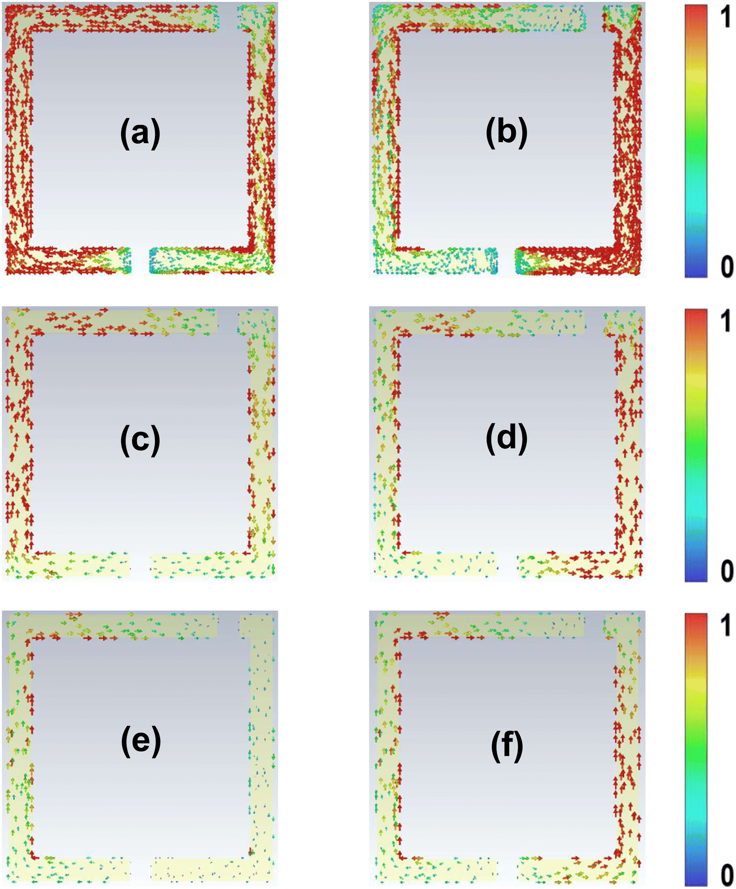 | ||
| Fig. 7 The surface current distributions of (a) the Fano resonance mode and (b) the dipole resonance mode of the TASR/quartz sample. (c, d) The surface current distributions of (c) the Fano resonance mode and (d) the dipole resonance mode of the CH3NH3PbI3/TASR/graphene/quartz sample with graphene and perovskite conductivity 10 S m−1. (e, f) The surface current distributions of (e) the Fano resonance mode and (f) the dipole resonance mode of the CH3NH3PbI3/TASR/graphene/quartz sample with graphene and perovskite conductivity 100 S m−1. | ||
However, for the dipole resonance mode, parallel surface currents are observed on the two arms of the TASR without gaps, resulting in the accumulation of homogeneous charges at both ends of the gaps. Thus, in the dipole resonant mode, the electric field intensity in the two gaps of the resonator is weaker than that in the Fano resonance mode, so the dipole resonance mode has lower sensitivity to changes in the material layer and its conductivity. These simulations explain the above experimental and simulation results.
It is worth noting that both the Fano resonance mode and the dipole resonance mode have strong surface current distributions in this simulation, so the resonance intensities of the two modes are very strong. Fig. 7(c) and (d) show the surface current distributions of the Fano and dipole modes, respectively, of the CH3NH3PbI3/TASR/graphene/quartz samples when the conductivity of the graphene and perovskite is 10 S m−1. The surface current distributions are weakened for both modes, so the addition of the graphene and perovskite affects both resonances.
Fig. 7(e) and (f) show the surface current distributions of the Fano and dipole resonance modes, respectively, of the CH3NH3PbI3/TASR/graphene/quartz samples when the conductivity of the graphene and perovskite is 100 S m−1. As the conductivities of the graphene and perovskite increase, the surface current distribution of the Fano mode is significantly weakened, while that of the dipole mode only slightly weakens. Again, changes in the conductivities of the graphene and perovskite mainly affect the Fano mode, while the dipole mode is only slightly affected.
It is well known that the performance and stability of optoelectronic devices based on perovskite materials are very sensitive to moisture and humidity in the environment because perovskite is easily degraded and damaged by water.61–64 Therefore, we investigated the effect of a humid environment on the actively-tunable hybrid terahertz metasurface device. First, we sprayed a layer of water mist uniformly on the surface of the CH3NH3PbI3/TASR/graphene/quartz sample (i.e. on the CH3NH3PbI3 layer) to simulate the degradation of CH3NH3PbI3 by water in humid air. Next, the sample was tested in the THz-TDS system to obtain the frequency-domain THz transmission signal without and with photoexcitation by a 780 nm laser at 250 mW cm−2. Under photoexcitation, the MD of the sample was only 0.6%, and the resonance intensities of both the Fano and dipole resonance modes were almost unchanged because of the water degradation of the CH3NH3PbI3 layer. However, it is worth noting that the resonance frequencies of the two modes still shifted significantly under photoexcitation. The frequency of the Fano resonance mode redshifted from 551 to 543 GHz, while that of the dipole resonance mode blueshifted from 1134 to 1137 GHz. Thus, the CH3NH3PbI3/TASR/graphene/quartz sample proposed in this study can be used as a frequency-tunable THz metasurface switch in a dry environment, while in a wet environment, it becomes a THz frequency-selective device. The above results are useful for practical applications of optoelectronic devices based on organometallic halide perovskite materials (Fig. 8).
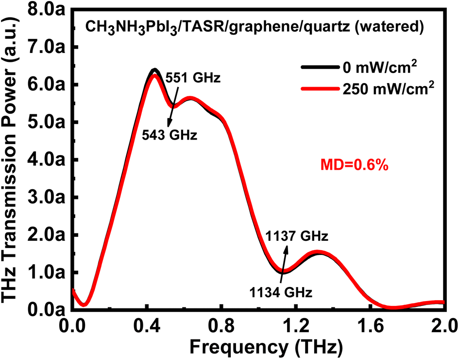 | ||
| Fig. 8 Frequency-domain THz transmission by the CH3NH3PbI3/TASR/graphene/quartz sample wetted with water mist without photoexcitation (black) and excited by a 780 nm continuous-wave laser at 250 mW cm−2 (red). | ||
4. Conclusion
In this work, we investigated the properties of an actively tunable, hybrid terahertz metasurface device comprising monolayer graphene, organometallic halide perovskite (CH3NH3PbI3), and a metasurface consisting of terahertz asymmetric split-ring resonators (TASR). The metasurface has two resonance modes: the one at lower frequency is the Fano resonance, while the one at higher frequency is the dipole resonance. With the addition of monolayer graphene and CH3NH3PbI3, the resonance intensities of the two modes are significantly weakened, and the resonance frequencies undergo a simultaneous redshift. When the sample is excited by 780 nm laser excitation at 250 mW cm−2, the THz transmission is significantly reduced, and multidimensional manipulation of the Fano resonance is achieved. However, the resonance intensity of the dipole mode is almost unchanged, and its frequency undergoes a blueshift. We explained the physical mechanism using equivalent transmission line theory and equivalent circuit models and verified the experimental results using a finite-difference time-domain simulation. Finally, we investigated the effect of moisture on device performance, and found that under photoexcitation, a sample wetted with water mist undergoes almost no modulation of the THz wave or the intensity of the resonance modes, but the resonance frequencies still shift significantly. This characterization provides a foundation for applications of hybrid metasurface devices based on organometallic halide perovskite and other semiconductor materials in realistic environments.Author contributions
The manuscript was written through contributions of all authors. All authors have given approval to the final version of the manuscript.Conflicts of interest
The authors declare no conflict of interest.Acknowledgements
This research was supported by National Natural Science Foundation of China (Grant No. 62175168 and 61505125), Nature Science Foundation of Beijing Municipality (Grant No. 4202013).References
- J. Huang, J. N. Li, Y. Yang, J. Li, J. H. Li, Y. T. Zhang and J. Q. Yao, Opt. Express, 2020, 28, 7018–7027 CrossRef PubMed.
- L. Peng, X. M. Li, X. Liu, X. Jiang and S. M. Li, Nanoscale Adv., 2019, 1, 1452–1459 RSC.
- N. I. Landy, S. Sajuyigbe, J. J. Mock, D. R. Smith and W. J. Padilla, Phys. Rev. Lett., 2008, 100, 207402 CrossRef CAS PubMed.
- L. Wang, Y. X. Zhang, X. Q. Guo, T. Chen, H. J. Liang, X. L. Hao, X. Hou, W. Kou, Y. C. Zhao, T. C. Zhou, S. X. Liang and Z. Q. Yang, Nanomaterials, 2019, 9, 965 CrossRef.
- J. E. Heyes, W. Withayachumnankul, N. K. Grady, D. R. Chowdhury, A. K. Azad and H. T. Chen, Appl. Phys. Lett., 2014, 105, 181108 CrossRef.
- Y. K. Srivastava, A. Chaturvedi, M. Manjappa, A. Kumar, G. Dayal, C. Kloc and R. Singh, Adv. Opt. Mater., 2017, 5, 1700762 CrossRef.
- X. Yan, Z. Zhang, L. J. Liang, M. S. Yang, D. Q. Wei, X. X. Song, H. T. Zhang, Y. Y. Lu, L. H. Liu, M. J. Zhang, T. Wang and J. Q. Yao, Nanoscale, 2020, 12, 1719–1727 RSC.
- R. Y. Zhou, C. Wang, Y. X. Huang, K. Huang, Y. L. Wang, W. D. Xu, L. J. Xie and Y. B. Ying, Biosens. Bioelectron., 2021, 188, 113336 CrossRef CAS PubMed.
- W. D. Xu, L. J. Xie, J. F. Zhu, L. H. Tang, R. Singh, C. Wang, Y. G. Ma, H. T. Chen and Y. B. Ying, Carbon, 2019, 141, 247–252 CrossRef CAS.
- X. Yan, T. T. Li, G. H. Ma, J. Gao, T. L. Wang, H. Y. Yao, M. S. Yang, L. J. Liang, J. Li, J. Li, D. Q. Wei, M. Wang, Y. X. Ye, X. X. Song, H. T. Zhang, C. Ma, Y. P. Ren, X. D. Ren and J. Q. Yao, Photonics Res., 2022, 10, 280–288 CrossRef.
- K. Sun, R. H. Fan, X. H. Zhang, Z. D. Zhang, Z. C. Shi, N. Wang, P. T. Xie, Z. Y. Wang, G. H. Fan, H. Liu, C. T. Liu, T. X. Li, C. Yan and Z. H. Guo, J. Mater. Chem. C, 2018, 6, 2925–2943 RSC.
- M. Manjappa, Y. K. Srivastava, A. Solanki, A. Kumar, T. C. Sum and R. Singh, Adv. Mater., 2017, 29, 1605881 CrossRef.
- S. Kaur, S. Karmakar, A. Jana, S. Rane, R. K. Varshney and D. R. Chowdhury, iScience, 2022, 25, 104024 CrossRef CAS.
- A. Poddubny, I. Iorsh, P. Belov and Y. Kivshar, Nat. Photonics, 2013, 7, 948–957 CrossRef.
- X. Zhang and Z. W. Liu, Nat. Mater., 2008, 7, 435–441 CrossRef PubMed.
- T. J. Yen, W. J. Padilla, N. Fang, D. C. Vier, D. R. Smith, J. B. Pendry, D. N. Basov and X. Zhang, Science, 2004, 303, 1494–1496 CrossRef PubMed.
- J. Valentine, S. Zhang, T. Zentgraf, E. Ulin-Avila, D. A. Genov, G. Bartal and X. Zhang, Nature, 2008, 455, 376–379 CrossRef.
- T. J. Cui, L. L. Li, S. Liu, Q. Ma, L. Zhang, X. Wan, W. X. Jiang and Q. Cheng, iScience, 2020, 23, 101403 CrossRef.
- J. Li, J. T. Li, Y. Yang, J. N. Li, Y. T. Zhang, L. Wu, Z. Zhang, M. S. Yang, C. L. Zheng, J. H. Li, J. Huang, F. Y. Li, T. T. Tang, H. T. Dai and J. Q. Yao, Carbon, 2020, 163, 34–42 CrossRef.
- L. P. Xia, Y. X. Zou, M. Zhang, W. J. Yan, S. H. Dang, S. B. Li, S. Y. Yin and H. L. Cui, Phys. Scr., 2019, 94, 125701 CrossRef CAS.
- C. Xu, Z. H. Ren, J. X. Wei and C. Lee, iScience, 2022, 25, 103799 CrossRef CAS PubMed.
- L. Y. Xiong, B. Liu, D. D. Liu, L. F. Lv, Y. B. Hou, J. L. Shen and B. Zhang, Nanoscale, 2020, 12, 3343–3350 RSC.
- Y. Li, W. B. Yan, Y. L. Li, S. F. Wang, W. Wang, Z. Q. Bian, L. X. Xiao and Q. H. Gong, Sci. Rep., 2015, 5, 14485 CrossRef CAS.
- Y. H. Lee, J. S. Luo, M. K. Son, P. Gao, K. T. Cho, J. Seo, S. M. Zakeeruddin, M. Grätzel and M. K. Nazeeruddin, Adv. Mater., 2016, 28, 3966–3972 CrossRef CAS.
- D. W. Yang, W. M. Ming, H. L. Shi, L. J. Zhang and M. H. Du, Chem. Mater., 2016, 28, 4349–4357 CrossRef CAS.
- H. M. Zhu, Y. P. Fu, F. Meng, X. X. Wu, Z. Z. Gong, Q. Ding, M. V. Gustafsson, M. T. Trinh, S. Jin and X. Y. Zhu, Nat. Mater., 2015, 14, 636–642 CrossRef CAS PubMed.
- J. Ghosh, R. Ghosh and P. K. Giri, ACS Appl. Nano Mater., 2018, 1, 1551–1562 CrossRef CAS.
- J. Ghosh, R. Ghosh and P. K. Giri, ACS Appl. Mater. Interfaces, 2019, 11, 14917–14931 CrossRef CAS.
- N. G. Park, M. Grätzel, T. Miyasaka, K. Zhu and K. Emery, Nat. Energy, 2016, 1, 16152 CrossRef CAS.
- K. S. Novoselov, A. K. Geim, S. V. Morozov, D. Jiang, Y. Zhang, S. V. Dubonos, I. V. Grigorieva and A. A. Firsov, Science, 2004, 306, 666–669 CrossRef CAS.
- Y. B. Zhang, Y. W. Tan, H. L. Stormer and P. Kim, Nature, 2005, 438, 201–204 CrossRef CAS.
- K. S. Novoselov, A. K. Geim, S. V. Morozov, D. Jiang, M. I. Katsnelson, I. V. Grigorieva, S. V. Dubonos and A. A. Firsov, Nature, 2005, 438, 197–200 CrossRef CAS.
- Y. P. Zhang, T. T. Li, B. B. Zeng, H. Y. Zhang, H. H. Lv, X. Y. Huang, W. L. Zhang and A. K. Azad, Nanoscale, 2015, 7, 12682–12688 RSC.
- B. S. Rodriguez, R. S. Yan, M. M. Kelly, T. Fang, K. Tahy, W. S. Hwang, D. Jena, L. Liu and H. G. Xing, Nat. Commun., 2012, 3, 780 CrossRef PubMed.
- T. Otsuji, S. A. B. Tombet, A. Satou, H. Fukidome, M. Suemitsu, E. Sano, V. Popov, M. Ryzhii and V. Ryzhii, MRS Bull., 2012, 37, 1235–1243 CrossRef CAS.
- A. Andryieuski and A. V. Lavrinenko, Opt. Express, 2013, 21, 9144–9155 CrossRef CAS.
- S. Y. Huang, C. Y. Song, G. W. Zhang and H. G. Yan, Nanophotonics, 2017, 6, 1191–1204 CAS.
- T. Otsuji, S. A. B. Tombet, A. Satou, H. Fukidome, M. Suemitsu, E. Sano, V. Popov, M. Ryzhii and V. Ryzhii, J. Phys. D: Appl. Phys., 2012, 45, 303001 CrossRef.
- X. L. Zhao, C. Yuan, L. Zhu and J. Q. Yao, Nanoscale, 2016, 8, 15273–15280 RSC.
- G. Jnawali, Y. Rao, H. G. Yan and T. F. Heinz, Nano Lett., 2013, 13, 524–530 CrossRef PubMed.
- C. J. Docherty and M. B. Johnston, J. Infrared Millim. Terahertz Waves, 2012, 33, 797–815 CrossRef.
- M. S. Yang, T. T. Li, X. Yan, L. J. Liang, H. Y. Yao, Z. Q. Sun, J. Li, J. Li, D. Q. Wei, M. Wang, Y. X. Ye, X. X. Song, H. T. Zhang and J. Q. Yao, ACS Appl. Mater. Interfaces, 2022, 14, 2155–2165 CrossRef.
- M. Y. Li, Y. T. Zhang, X. Tang, J. T. Li, S. L. Wang, T. T. Li, H. L. Zhao, Q. Y. Li, Q. Wang and J. Q. Yao, J. Alloys Compd., 2022, 895, 162496 CrossRef.
- H. Y. Yao, Z. Q. Sun, X. Yan, M. S. Yang, L. J. Liang, G. H. Ma, J. Gao, T. T. Li, X. X. Song, H. T. Zhang, Q. L. Yang, X. F. Hu, Z. Q. Wang, Z. H. Li and J. Q. Yao, Nanophotonics, 2022, 11, 1219–1230 CrossRef.
- W. J. Wang, L. H. Du, J. Li, M. Z. Hu, C. L. Sun, Y. J. Zhong, G. Zhao, Z. R. Li, L. G. Zhu, J. Q. Yao and F. R. Ling, Opt. Express, 2021, 29, 12712–12722 CrossRef.
- C. Li, J. B. Wu, S. L. Jiang, R. F. Su, C. H. Zhang, C. T. Jiang, G. C. Zhou, B. B. Jin, L. Kang, W. W. Xu, J. Chen and P. H. Wu, Appl. Phys. Lett., 2017, 111, 092601 CrossRef.
- Y. Z. Hu, M. Y. Tong, S. Y. Hu, W. B. He, X. A. Cheng and T. Jiang, Nanophotonics, 2022, 11, 1367–1378 CrossRef.
- X. Li, T. T. Yang, Y. Q. Liu, J. Y. Liu, B. Liu, L. F. Lv, Y. B. Hou, Y. Zhang, J. L. Shen and B. Zhang, J. Phys. D: Appl. Phys., 2021, 54, 325102 CrossRef.
- X. Li, T. T. Yang, J. S. He, F. H. Wang, J. L. Shen and B. Zhang, ACS Appl. Electron. Mater., 2022, 4, 1832–1840 CrossRef.
- L. Q. Cong, M. Manjappa, N. N. Xu, I. Al-Naib, W. L. Zhang and R. Singh, Adv. Opt. Mater., 2015, 3, 1537–1543 CrossRef.
- L. Q. Cong, Y. K. Srivastava, A. Solanki, T. C. Sum and R. Singh, ACS Photonics, 2017, 4, 1595–1601 CrossRef.
- R. Singh, I. A. I. Al-Naib, M. Koch and W. L. Zhang, Opt. Express, 2011, 19, 6312–6319 CrossRef PubMed.
- Q. Li, L. Q. Cong, R. Singh, N. N. Xu, W. Cao, X. Q. Zhang, Z. Tian, L. L. Du, J. G. Han and W. L. Zhang, Nanoscale, 2016, 8, 17278–17284 RSC.
- A. Rastgordani, Z. G. Kashani and M. S. Abrishamian, Optik, 2020, 221, 165354 CrossRef.
- Z. M. Liu, L. Guo and Q. M. Zhang, Nanomaterials, 2019, 9, 1351 CrossRef PubMed.
- S. J. Kindness, N. W. Almond, B. B. Wei, R. Wallis, W. Michailow, V. Kamboj, P. Braeuninger-Weimer, S. Hofmann, H. E. Beere, D. A. Ritchie and R. Degl'Innocenti, Adv. Opt. Mater., 2018, 6, 1800570 CrossRef.
- S. Asgari and T. Fabritius, Opt. Express, 2020, 28, 39850–39867 CrossRef.
- T. T. Yang, X. Li, Y. Q. Liu, J. Y. Liu, B. Liu, G. C. Wang, L. F. Lv, Y. B. Hou, F. Teng, Y. Zhang, J. L. Shen and B. Zhang, Opt. Mater., 2021, 120, 111470 CrossRef.
- A. Thoman, A. Kern, H. Helm and M. Walther, Phys. Rev. B, 2008, 77, 195405 CrossRef.
- C. J. Docherty, C. T. Lin, H. J. Joyce, R. J. Nicholas, L. M. Herz, L. J. Li and M. B. Johnston, Nat. Commun., 2012, 3, 1228 CrossRef PubMed.
- J. B. Huang, S. Q. Tan, P. D. Lund and H. P. Zhou, Energy Environ. Sci., 2017, 10, 2284–2311 RSC.
- W. H. Zhang, J. Xiong, J. H. Li and W. A. Daoud, Sol. RRL, 2020, 4, 1900370 CrossRef.
- M. T. Hoang, N. D. Pham, J. H. Han, J. M. Gardner and I. Oh, ACS Appl. Mater. Interfaces, 2016, 8, 11904–11909 CrossRef PubMed.
- C. C. Lin, D. H. Jiang, C. C. Kuo, C. J. Cho, Y. H. Tsai, T. Satoh and C. Su, ACS Appl. Mater. Interfaces, 2018, 10, 2210–2215 CrossRef PubMed.
| This journal is © The Royal Society of Chemistry 2023 |