
 Open Access Article
 This Open Access Article is licensed under a Creative Commons Attribution-Non Commercial 3.0 Unported Licence
Redox-active ions unlock substitutional doping in halide perovskites†
Zuzanna
Molenda
 ac,
Bastien
Politi
b,
Raphaël
Clerc
b,
Mamatimin
Abbas
a,
Sylvain
Chambon
a,
Dario M.
Bassani
*c and
Lionel
Hirsch
*a
ac,
Bastien
Politi
b,
Raphaël
Clerc
b,
Mamatimin
Abbas
a,
Sylvain
Chambon
a,
Dario M.
Bassani
*c and
Lionel
Hirsch
*a
aUniv. Bordeaux, CNRS, Bordeaux INP, IMS, UMR 5218, F-33400 Talence, France. E-mail: lionel.hirsch@ims-bordeaux.fr
bUniversité de Lyon, Université Jean Monnet-Saint-Étienne, CNRS, Institut d’Optique Graduate School, Laboratoire Hubert Curien, UMR 5516, F-42023 Saint-Etienne, France
cUniv. Bordeaux, CNRS, Bordeaux INP, ISM UMR 5255, F-33400 Talence, France. E-mail: dario.bassani@u-bordeaux.fr
First published on 6th July 2023
Abstract
Electrical doping of metal halide perovskites (MPHs) is a key step towards the use of this efficient and cost-effective semiconductor class in modern electronics. In this work, we demonstrate n-type doping of methylammonium lead iodide (CH3NH3PbI3) by the post-fabrication introduction of Sm2+. The ionic radius of the latter is similar to that of Pb2+ and can replace it without altering the perovskite crystal lattice. It is demonstrated that once incorporated, Sm2+ can act as a dopant by undergoing oxidation to Sm3+. This results in the release of a negative charge that n-dopes the material, resulting in an increase of conductivity of almost 3 orders of magnitude. Unlike substitution doping with heterovalent ions, furtive dopants do not require counterions to maintain charge neutrality with respect to the ions they replace and are thus more likely to be incorporated into the crystalline structure. The incorporation of the dopant throughout the material is evidenced by XPS and ToF-SIMS, while the XRD pattern shows no phase separation at low and medium doping concentrations. A shift of the Fermi level towards a conduction energy of 0.52 eV confirms the doping to be n-type with a charge carrier density, calculated using the Mott–Schottky method, estimated to be nearly 1017 cm−3 for the most conductive samples. Variable-temperature conductivity experiments show that the dopant is only partially ionized at room temperature due to dopant freeze-out.
New conceptsMetal halide perovskites have demonstrated their ability to combine excellent optoelectronic properties with printing processes. Nevertheless, the control of their doping remains a challenge for both fundamental sciences and industrial applications. Whereas several examples of p-type doping have been reported in the literature, n-type doping is trickier and only a few reports with no or poor doping efficiency exist. Our paper reports a totally new approach using metastable ions to n-doped halide perovskite semiconductors leading to an increase of 3 orders of magnitude of the conductivity and shift of the Fermi level towards a conduction energy of 0.52 eV. This new method using redox active ions is unique in that it mimics the classical substitutional doping used with great success in covalent semiconductors (Si, GaAs, etc.). |
1. Introduction
The rapid development of metal halide perovskite (MHP) photovoltaic devices owes much to pre-existing knowledge gained from both inorganic semiconductors (band structures, photon absorption, charge transport, etc.) and organic semiconductors (wet processes, soft substrates, etc.). However, as pointed out in the reviews by Brenner et al.1 and Fakharuddin et al.,2 the critical role of surface properties and interface quality in the operation of MHP-based devices and their stability has emerged as one of the major challenges limiting the development of these technologies. While we can consider that this is generally true for any type of thin film device, in the case of inorganic semiconductors (and for silicon-based devices in particular), this difficulty is partially solved by using well-controlled doping. Indeed, doping allows combining contacting metal electrodes with highly doped semiconductor layers, removing interfaces away from the carrier collection area. Moreover, connecting semiconductors through highly doped interfacial layers render the contact almost insensitive to the value of the metal WF, giving more flexibility in selecting metals as electrodes. In the case of MHPs, well-controlled doping would allow the design of more complex devices based on the p–n junction concept, making the emerging perovskite-based technology architecturally compatible to current inorganic semiconductors.3One may note that the term “doping” is overused in the perovskite community because it is often confused with the use of additives impacting the crystallinity or surface passivation of the active layer and their effects on solar cell efficiency rather than to the precise control of the conductivity of the semiconductor. The difficulty in achieving electrical doping of MHPs is a consequence of the ionic crystalline nature of the material. Whereas dopants can be introduced in inorganic semiconductors during the growth process or through thermal evaporation, doping of MHPs requires the introduction of heterovalent ions whose charge differs from that of the pristine material's constituent ions. For example, p-type doping could in principle be achieved through the introduction of Bi3+ as reported by Abdelhady et al.4 However, preservation of charge neutrality entails that its incorporation be accompanied by three monovalent counteranions, which is highly disfavored during crystallization as this is incompatible with the crystal lattice. Thus, current doping strategies for MHPs, apart from the intentional formation of defects to provide extra electrons or holes to the lattice,5 are concentrated on substitutional doping using electrochemical methods6 or on the use of molecular dopants. The latter strategy was nicely demonstrated through the use of tetrafluorotetracyanoquinodimethane (F4TCNQ) to enhance the electrical conductivity of MASn0.5Pb0.5I3 by over 4 orders of magnitude (MA = methylammonium). In this approach, the neutral, strongly electron-accepting molecular dopant was not incorporated into the crystalline grains but instead located at the grain boundaries.7 Both the high electron affinity of F4TCNQ and the interaction of fluorinated carbon species on the halide hybrid perovskite8 allowed for efficient charge transfer. n-Type doping is apparently trickier to achieve because only a few examples have been published and none of them seem efficient. Zhang et al.9 performed Hall and Mott–Schottky measurements to demonstrate the n-type doping with Sb. Nevertheless, the variation of the charge carrier density is less than a factor of 2 (in the best case) that is clearly in the error bar of this technique. Han et al.10 used CaCl2 as the dopant. In their case, they do not want to target substitution but they use a bilayer for the doping. The authors expect electron transfer from the conduction band of CaCl2 to the conduction band of the perovskite. However, the efficiency is poor since the electron density in CaCl2 is extremely low. Zhang et al.11 reported n-type doping with the introduction of AgI in the perovskite. They observed an increase of current for electron only devices in the space charge limited current (SCLC) plot for the doped perovskite. This increase is less than one order of magnitude. Nevertheless, they did not determine the Fermi level variation or the charge carrier density.
In this paper, we present a totally new method to n-dope halide perovskites leading to an enhancement of 3 orders of magnitude of the conductivity. We demonstrate that n-type doping of MHPs is possible by introduction of furtive heterovalent atoms. The latter are metastable ions whose charge and ionic radius are identical or very similar to one of the constituent ions of the MHP. For example, ions whose ionic radius is similar to that of the Pb2+ ion (1.19 Å)12 but that are metastable at the 2+ valence state could impart n-doping upon substitutional doping of Pb2+ followed by oxidation to the +3 state and release of an electron. To demonstrate the validity of this approach, we focused on n-type doping since this is still unreported for MHPs and, combined with previously reported p-type doping methods, could open the way for MHP-based semiconductor logic devices. Screening of the periodic table reveals several candidates that fit these requirements, such as Pd2+ or Sn2+ that are also stable in the Pd3+ and Sn4+ oxidation states. However, the ionic radii of their 2+ ions are somewhat smaller than that of Pb2+.13,14 We thus turned our attention to samarium, as both Sm2+ and Sm3+ possess ionic radii that are similar to Pb2+ (1.27 Å and 1.13 Å, for Sm2+ and Sm3+, respectively15). Furthermore, SmI2, also known as Kagan's reagent, is a stable, well-known single-electron reductant widely used in organic synthesis.16 It is highly reducing, with a half-wave potential of −0.89 V vs. SCE that is significantly increased upon coordination.17 Trivalent lanthanide ions and more specifically Sm3+ have already been used as optical dopants (but not for electrical doping) in perovskite nanocrystals and to increase the stability of fully inorganic perovskite of solar cells.18–20 We selected the well-known methylammonium lead triiodide (CH3NH3PbI3 or MAPI) as a prototypical MHP material, but show that the approach is also valid for formamidium-based MHPs and mixed cation perovskites.
2. Methods
Materials
Lead(II) acetate trihydrate (PbAc2·3H2O, 5N) was purchased from Sigma Aldrich. Methylammonium iodide (CH3CN3I, > 4N) was purchased from GreatCell Solar Materials. Samarium(II) iodide (SmI2, 4N) was purchased from Alfa Aesar. Anhydrous N,N-dimethylformamide (DMF) and anhydrous isopropanol were purchased from Sigma Aldrich.Sample preparation
Three types of substrates were used according to the characterization technique used. For conductivity measurements, glass substrates with patterned gold electrodes were used. For AFM XRD, absorption and PL spectroscopy, bare glass substrates were sufficient, while for the SEM, XPS, ToF SIMS and Kelvin probe force microscopy, glass substrates covered with a thin layer of ITO (10 Ω sq−1) were selected.Sample fabrication
The substrates were cleaned in a sonication bath first with Hellmanex™ III solution (Sigma Aldrich) and in DI water for 15 minutes each and then in isopropanol (4N) for 10 min. Subsequently, they were treated with a UV-ozone for 15 minutes. Sample fabrication was performed under a controlled atmosphere in a glove box. The perovskite precursor solution was prepared by dissolving 0.72 M PbAc2·3H2O and 2.2 M MAI in DMF and stirring at room temperature for 30 min. The solution was filtered through a 0.45 μm PTFE filter and spin coated at a spin rate of 2500 rpm for 2 min. The sample was then dried at RT for 3 min and annealed for 25 min at 100 °C. The perovskite film thickness was around 270 nm. SmI2 was dissolved in isopropanol and DMF (0.1% v/v) and stirred overnight at RT. The solution was filtered with a 0.45 μm PTFE filter and spin coated at a spin rate of 2500 rpm for 1 min. The sample was placed on the hot plate at 100 °C for 10 min.Characterization
Conductivity was calculated from the IV curves that were collected using a Keithley 4200 source meter unit (SMU). The samples were scanned from −1 V to 1 V at a rate of 5 mV s−1. For the temperature dependent conductivity measurements, a Biologic SP-200 potentiostat was used and the temperature was controlled using an Omron E5AN cryostat. For the AFM images, a Bruker NanoScope instrument was used in a tapping mode. X-ray diffraction (XRD) patterns were obtained using a Bruker D2 Phaser, absorption spectra were recorded using a Shimadzu UV-3600 Plus UV-Vis-NIR spectrophotometer, and photoluminescence spectra were recorder using a Photon Technology International setup, model: P21LRXS-LNN-NS-17. SEM images were made using a SEM-FEG HR (JEOL 6700F), ToF SIMS profiles were obtained using TOF.SIMS 5 ION-TOF and argon clusters were used for in-depth sputtering. XPS spectra were recorded using a K-Alpha ThermoFisher Scientific spectrometer and the in-depth profiles were obtained by etching the surface with argon ions. The work function was measured using a Kelvin probe station. UPS was performed using a PHOIBOS 100 hemispherical energy analyzer, equipped with the SPECS UVS 10/35 light source. All the characterization procedures were performed in a controlled atmosphere or on the encapsulated samples.3. Results and discussion
The process of crystallization concentrates impurities in the mother liquor from which these may precipitate onto the crystal surface upon its evaporation.21 Similarly, doping of micro- or nano-crystalline thin films remains a challenge since most of the dopant resides on the surface or at grain boundaries.22,23 Aware of these challenges, and the fact that SmI2 is highly reactive towards traces of moisture and impurities in solution, we developed a doping method for MAPI thin films that is based on a two-step spin coating process. First, the perovskite layer is spin coated and annealed (thickness = 270 nm). Second, an SmI2 solution is spin coated on top of the perovskite film and dried to evaporate the rest of the solvent. The solvent used for SmI2 is isopropanol (that does not dissolve the perovskite) and 0.1% v/v DMF. The small addition of DMF strongly enhances the wettability of the solution.In order to validate the doping method, we measured the conductivity of the doped and undoped materials as a function of the dopant concentration in solution. Conductivity measurements were performed using bottom gold electrodes in the two probe configuration on the lateral geometry in order to avoid any artifacts due to possible pinholes in the vertical geometry (Fig. S1, ESI†). The effect on the conductivity of the perovskite layer from the SmI2 treatment is shown in Fig. 1(a) and evidences an increase in the conductivity of the MHP that depends on the concentration of the dopant in solution. An increase of about 3 orders of magnitude is observed at an SmI2 concentration of 10 mg mL−1 (from 10−8 S cm−1 to almost 10−5 S cm−1). Control experiments using a neat solvent (0 mg mL−1) or a bare SmI2 layer show that neither alone is responsible for the increase in conductivity. In fact, the conductivity of an SmI2 layer is even lower than that of the undoped perovskite layer, therefore excluding residual SmI2 on the top of the perovskite layer as the reason for such an enhancement. We therefore attribute to the increase of conductivity to the combination of SmI2 and MAPI by the chemical reduction of the latter. To confirm this, we investigated the impact of SmI3 treatment on the conductivity, using the same molar concentration and experimental condition as with SmI2 (Fig. 1(b)). One can clearly see that only SmI2 leads to a significant enhancement of the perovskite layer's conductivity. The concept of doping described above is expected to work not only for MAPI, but for other perovskites as well. Indeed, formamidinium lead iodide (FAPbI3) and a mixed cation MA0.07FA0.93PbI3, doped with SmI2, using the same procedure as for MAPI, demonstrated an increased conductivity by up to 2 and 2.5 orders of magnitude, respectively (see the ESI† for details, Fig. S3).
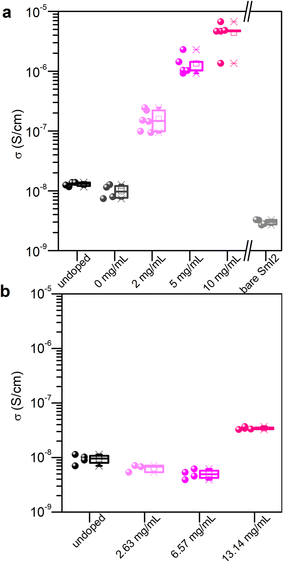 | ||
| Fig. 1 Conductivity as a function of doping with (a) SmI2 and (b) SmI3. 0 mg mL−1 describes the sample treated with the doping solvent only. For higher doping concentrations, see Fig. S2 (ESI†). | ||
Doping of a semiconductor results in an increase in the charge carrier density that in turn generates an increase in the material's conductivity. However, the observation of the latter phenomenon is not a sufficient proof of doping, as conductivity is the product of charge carrier density and mobility. In order to obtain more details on the origin of the conductivity enhancement, we characterized the doping type (n or p) and carried out analyses of (i) the samarium distribution on the surface or in the bulk of the layer; (ii) the proportion of Sm2+ and Sm3+ in the perovskite layer; (iii) and the impact of SmI2 on the perovskite crystal structure.
The two-step method used for the doping consists of depositing SmI2 on top of the active layer. To investigate whether the dopant remained on the surface or was distributed throughout the material, we used time of flight secondary ion mass spectroscopy (ToF-SIMS) with ion sputtering on the surface to track the elemental composition of the thin film throughout the layer. The results obtained show that the signal corresponding to Sm is detected throughout the active layer up to the appearance of the In signal corresponding to the ITO substrate (Fig. S4, ESI†). From this, we conclude that the dopant is incorporated throughout the perovskite layer during the second annealing step.
Oxidation of Sm2+ to Sm3+ is expected to release a free electron into the conduction band. We therefore used XPS (Fig. S5 and S6, ESI†) to determine the oxidation state of Sm inside the perovskite layer since each Sm valence state has a specific signature.24,25 In Fig. 2, the Sm 3d5/2 region of the spectrum of the SmI2 layer spin coated on the ITO substrate is shown, together with the spectra of the Sm-doped perovskite with 2, 5 and 10 mg mL−1 doping solution concentrations. The spectra of the perovskite layers were collected at a depth of ca. 200 nm in order to avoid the contribution of the surface layer that may be altered due to the doping method. Moreover, the oxygen signal is negligible whereas at the surface one can clearly see some contamination with oxygen (Fig. S7, ESI†) even though a transfer box was used to transport the samples from the nitrogen filled glovebox ([O2] < 1 ppm and [H2O] < 1 ppm) to the XPS vacuum chamber. This surface contamination explains why the XPS analysis of the SmI2 reference layer (20 nm) shows the presence of both Sm2+ and Sm3+. In the doped MHP samples, the Sm2+/Sm3+ ratio decreases to almost zero in agreement with the hypothesis that each Sm2+ doping ion undergoes oxidation and releases an electron once located in the perovskite layer. One can also observe a small shift of the binding energy of the Sm3+ peak between the SmI2 layer and the doped perovskite layers. The environment of Sm2+ and Sm3+ is different between the native SmI2 and the doped perovskite samples. In other words, this observation is consistent with a substitutional position of Pb2+ by Sm3+. The main peak in the XRD pattern is also slightly shifted for the doped samples towards lower diffraction angles (see Fig. 2(b)), indicating the expansion of the perovskite crystal lattice. This fine variation is not an artefact since the error due to the experimental setup has been corrected using the PbI2 peak as the reference (Fig. S9b, ESI†). Considering that the ionic radius of Sm2+ is bigger than that of Pb2+ (1.27 Å > 1.19 Å), it is expected that samarium ions are in the oxidation state 2+ at the time of crystallization. Thus, both XPS and shifts in the diffraction pattern are compatible with the hypothesis of ionic substitution.
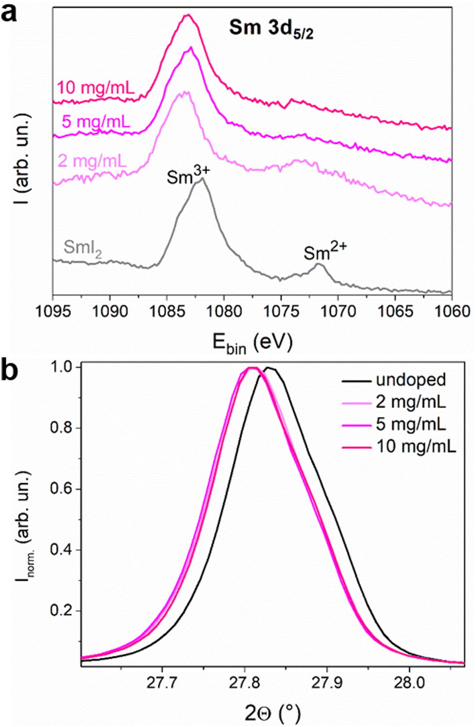 | ||
| Fig. 2 (a) XPS spectra of a thin film of SmI2 and perovskite thin films with different doping concentrations. The spectra are separated on the Y-axis for clarity. (b) Normalized X-ray diffraction (200) peaks of undoped and doped MAPI films. | ||
Characterization of the 10 mg mL−1 doped MHP surface using AFM and SEM (Fig. 3(e) and (f)) shows significantly different topologies than those of the undoped sample (Fig. 3(a) and (b)). While on the surface of the undoped perovskite grains with a size in the range of 100–500 nm are clearly seen, the doped layer is covered with the oval-like shared grains of a much smaller size (between 50 and 100 nm). The small grains on the surface of the doped sample are assigned to the presence of residual SmIx or SmOx. As expected, the sample treated with only solvent (Fig. 3(c) and (d)) did not show any alteration in morphology to the untreated sample.
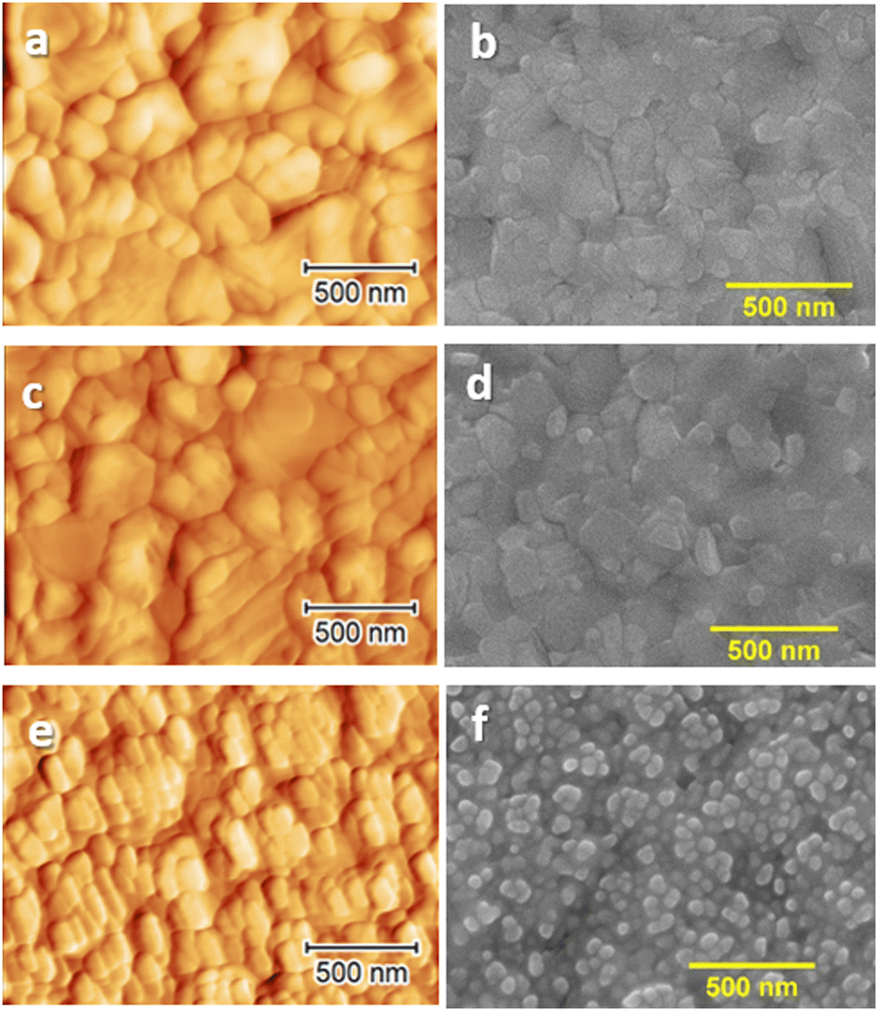 | ||
| Fig. 3 Surface AFM (a), (c), and (e) and SEM (b), (d), and (f) images of undoped MAPI films (a) and (b), MAPI treated with the dopant solvent (c) and (d) and MAPI doped with 10 mg mL−1 SmI2. For higher doping concentrations, see Fig. S8 (ESI†). | ||
To determine the impact of doping treatment on the crystal structure of the MAPI layer, X-ray diffraction (XRD) analyses were carried out (Fig. 4). The XRD spectra of the undoped sample and those doped with SmI2 concentrations of 2–10 mg mL−1 exhibit a diffraction pattern that is characteristic of tetragonal MAPI,26 with diffraction peaks at 13.6°, 27.8°, 31.3°, 42.6° and 58.3° that correspond to the (110), (220), (213), (330) and (440) Miller planes, respectively. Small peaks corresponding to PbI2 at 12.1° and 25.0° are also present, which is not uncommon in MAPI thin films.27 The identical positions of the principal diffraction peaks indicate that the crystal structure of the perovskite remains unchanged upon doping. A decrease in the peak intensity with the increasing dopant concertation suggests, however, that the incorporation of the dopant renders the polycrystalline layers more defective.
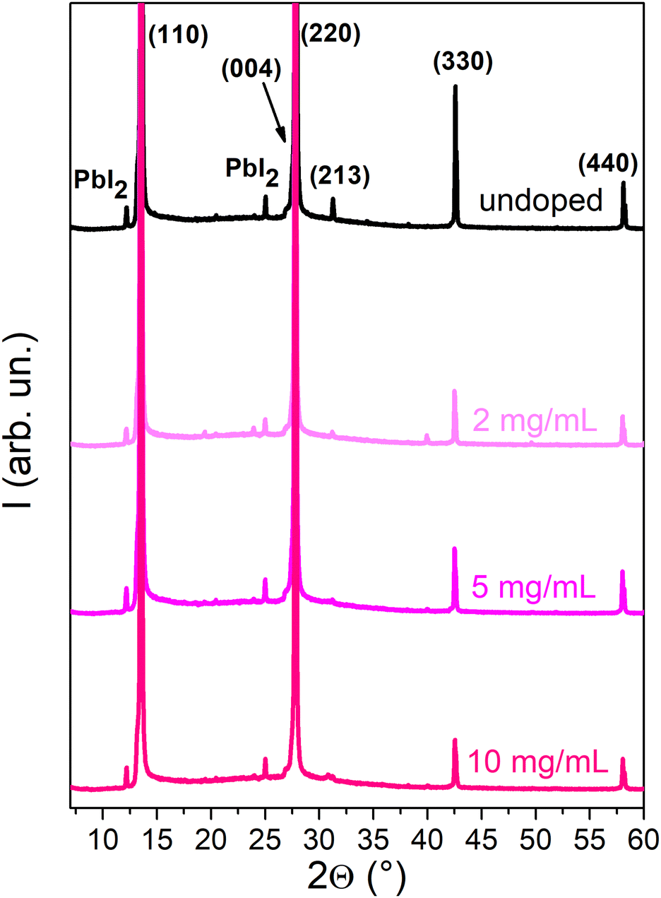 | ||
| Fig. 4 XRD spectra of the undoped MAPI film and MAPI doped with concentrations of 2–20 mg mL−1. For higher doping concentrations, see Fig. S9 (ESI†). | ||
Doping of a perovskite semiconductor would not be expected to alter the material's bandgap. To verify this, Fig. 5 shows the electronic absorption spectra of MHP layers with various doping concentrations. The absorption edge at 765 nm, typical for MAPI, is unaltered for all the doping concentrations. The bandgap energy (1.61 eV), extrapolated from the Tauc plots, is therefore the same for the doped and undoped MAPI samples. This excludes that the increase of the conductivity observed upon doping can be due to a reduction of the injection barrier and/or to additional energy bands within the bandgap.
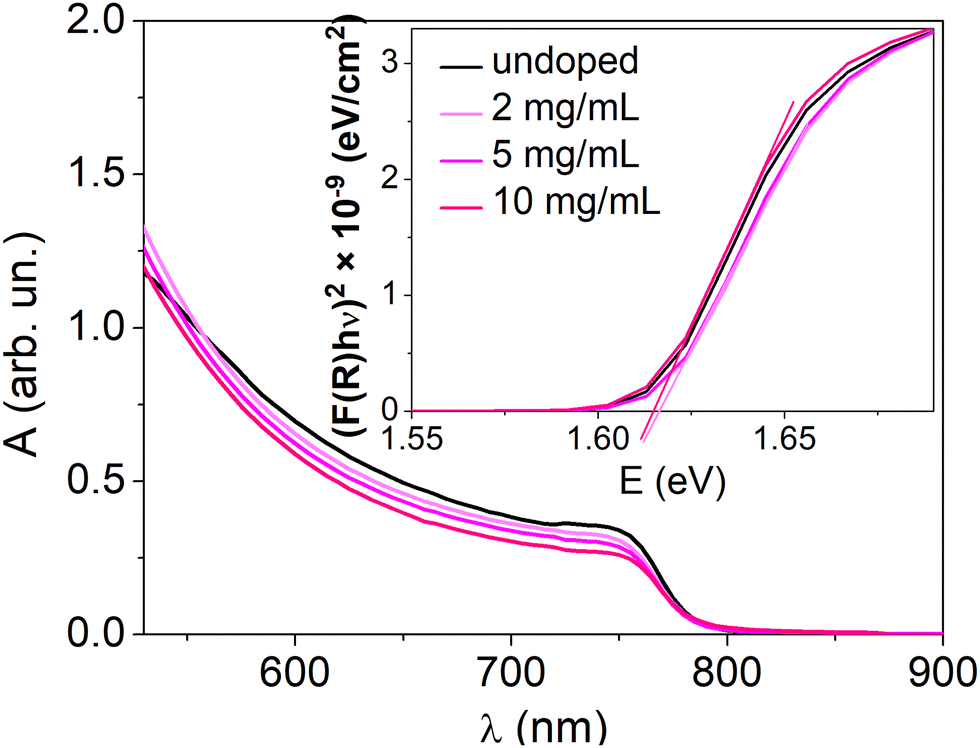 | ||
| Fig. 5 UV-visible absorption spectra of the undoped and doped perovskite thin films. The inset presents the Tauc plots for these samples. For higher doping concentrations, see Fig. S10 (ESI†). | ||
According to the propensity of Sm2+ to undergo oxidation, we expect that the resulting material will be n-doped. To confirm the majority charge carrier type, ultraviolet photoelectron spectroscopy (UPS) experiments were carried out to measure the variation of the WF versus the dopant concentration. The results of the surface potential difference measurements using a Kelvin probe (KP) (Fig. S11, ESI†) showed that for all the concentrations for which an increase in the conductivity is observed (2–10 mg mL−1), the WF saturates at the same level. Therefore, lower concentrations were chosen for the UPS experiments. In Fig. 6, the secondary electron cut-off region, corresponding to the WF of the material is presented for undoped MAPI and MAPI samples treated with solutions containing 0.01–10 mg mL−1 SmI2. A decrease of the WF from 4.51 eV for the undoped MAPI to 3.98 eV is observed for dopant concentrations as low as 0.01 mg mL−1. Instead, for dopant concentrations between 0.1 and 10 mg mL−1, the WF differs only by 0.11 eV. WF defines the position of EF with respect to the vacuum level (Evac), which is different for every material and can change due to the presence of surface dipoles. In order to define the position of EF in the bandgap, the valence band region of the UPS spectra was also analyzed. Due to the low density of states in the valence band in perovskites, the valence region analysis requires subtracting the satellites coming from the non-monochromatic radiation of the He lamp28,29 (Fig. S12 and S13, ESI†). Fig. 6(b) shows the valence band onset energy with respect to EF for different dopant concentrations. The intersection of the average background level with the extrapolation of the linear part of the valence band onset allows the determination of the ionization energy with respect to the Fermi level (E w.r.t. EF) (for more details, see Fig. S14, ESI†). For the undoped MAPI samples, the absolute value of this difference is around 0.83 eV, placing EF in the middle of the bandgap.30 The position of EF increases along with the dopant concentration, reaching ∼0.3 eV below EC at dopant concentrations of ≥0.2 mg mL−1. This clearly demonstrates the n-type character of the doped samples. For the doped samples, Evac changed by around –0.3 eV, which can be interpreted as the energy of the surface dipoles (Eμ) resulting probably from the altered surface composition due to the doping method. The energy of the surface dipole for the undoped MAPI was therefore assumed to be close to zero. The energy levels are schematically presented in Fig. 6(c) for different doping concentrations and the values of E w.r.t. EF, WF and Eμ are tabulated in Table 1.
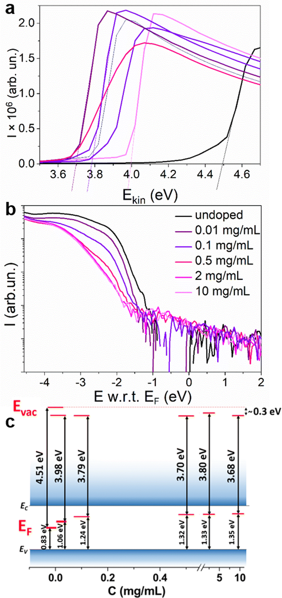 | ||
| Fig. 6 Secondary electron cut-off region (a) and valence band onset (b) of the undoped MAPI film and MAPI doped with 0.01–10 mg mL−1 SmI2, measured with UPS and concluded energy levels for the corresponding doping concentrations (c). | ||
| C (mg mL−1) | 0 | 0.01 | 0.1 | 0.5 | 2 | 10 |
| E w.r.t. EF (eV) | −0.83 | −1.06 | −1.24 | −1.32 | −1.33 | −1.35 |
| WF (eV) | 4.51 | 3.98 | 3.79 | 3.70 | 3.80 | 3.68 |
| E μ (eV) | 0 | −0.3 | −0.31 | −0.32 | −0.21 | −0.31 |
Estimation of the ionized dopant concentration was performed using the Mott–Schottky method.31 The voltage dependent capacitance measurement (C(V)) consists of measuring the small impedance signal of the device under tests as a function of an applied voltage V and a frequency f. In order to measure the capacitance accurately, the leakage current should be minimized. To this end, a capacitor structure was fabricated using a thin layer of insulating poly(methylmethacrylate) (PMMA) between the MAPI and the gold electrode. This particular structure includes a blocking contact at the MAPI/PMMA/gold interface and an ohmic contact at the MAPI/SnO2 side of the sandwich structure (Fig. S15, ESI†). Despite these precautions, the leakage current was not completely negligible over the full applied voltage range; consequently, the capacitance data exploited in this work were limited to the voltage range where G ≪ Cω, where G is the conductance and ω = 2πf. In this case, it was verified that the measured capacitance in a parallel or a series mode was the same. It is also well known that the analysis of C(V) measurements on perovskite semiconductors is affected by the motion of mobile ions.32–34 To prevent the contribution of mobile ions to the small capacitance signal and the increase of Cω, the frequency was set to 100 kHz (see Fig. S16, ESI†). Ionic motion may also have an impact on the device electrostatics when sweeping the voltage, leading to the hysteresis phenomenon.35 To minimize hysteresis, the voltage sweep rate was set at 120 mV s−1.
The Mott–Schottky analysis starts with plotting 1/C2versus the applied voltage. In the depletion regime, the 1/C2 curve should be linear with a slope equal to 2/(qεN+d), where q is the elementary charge, ε is the MAPI dielectric permittivity and N+d is the average ionized dopant concentration. As pointed out by Kirchartz et al.36 and supported by Fig. S17 (ESI†), this method requires that the depletion length remains lower than the layer thickness (270 nm). Because the depletion length increases when the doping level decreases, the ionized dopant concentration has to be higher than 1.1 × 1016 cm−3 to be able to detect a variation of the capacitance with an applied bias close to 0 V. Experimental 1/C2 curves versus voltage are shown in Fig. 7. For lower doping concentrations, the C(V) curve tends to saturate at a constant value when a high reverse bias is applied. This saturation occurs when the depletion layer extends beyond the layer thickness. We therefore note that the charge carrier concentration for our undoped sample is lower than the limit of detection of the Mott–Schottky method.36–38 Even though one can notice a slight excess of PbI2 revealed by XRD (Fig. 4) that could be responsible for unintentional doping, UPS confirms that the Fermi level is almost in the middle of the bandgap (Fig. 6). We may then assume that our reference is undoped and use the typical intrinsic charge carrier density for intrinsic MAPI that is in the range of 1011 cm−3.23 For doped samples, a clear linear trend was obtained in all cases allowing the extraction of the ionized dopant concentration, ranging from 2 × 1016 cm−3 for 2 mg mL−1 to 9.8 × 1016 cm−3 for 10 mg mL−1. This value is quite low compared to XPS analyses where we measured samarium concentrations in the range of Nd ∼ 1020 cm−3.
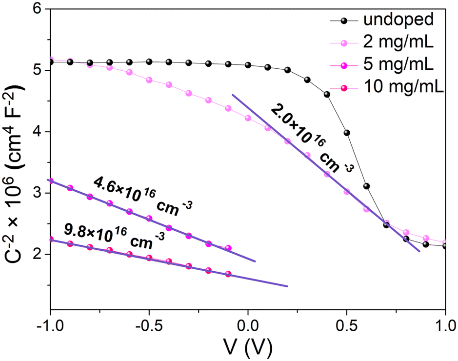 | ||
| Fig. 7 Mott–Schottky plots with extracted ionized dopant densities for different doping concentrations. Note that the concentration of the undoped sample is below the limit of detection. | ||
In order to elucidate the discrepancy between the ionized dopant concentration extracted by Mott–Schottky and samarium concentrations determined by XPS, conductivity measurements as function of temperature were carried out. We limited our investigation to the sample that exhibits the highest conductivity (10 mg mL−1) and the undoped sample as the reference. The measurement of the conductivity as a function of temperature was performed by cooling the sample from 373 K to 188 K (Fig. 8). The activation energy Ea is determined from the slope of the Arrhenius plot. Above 250 K, Ea is the same for both doped and undoped samples (Ea1 = 500 meV) even though the conductivity increases upon doping. For the doped sample below 250 K, a different slope can be distinguished, characterized by a lower activation energy Ea2 = 350 meV. These results can be interpreted as the competition between two mechanisms impacting the temperature dependence of the conductivity. The first mechanism with Ea1 = 500 meV is the same in both doped and undoped samples and probably corresponds to the thermal activation of carrier transport through grain boundaries. The second mechanism at T < 250 K and Ea2 = 350 meV is observed only for the doped samples. This second mechanism can be observed only at low temperatures. For T < 250 K, the thermal activation of mechanism 1 is not efficient and charge transport through grain boundaries probably occurs by tunneling (that is almost not thermally activated). Therefore, the second mechanism becomes the main limiting charge carrier transport. The temperature dependence of the doping ionization is consistent with the occurrence of dopant freezing, which in this case is observed even at room temperature. Such dopant freeze-out may explain the discrepancy between Mott–Schottky and XPS measurements, as the prior is sensitive only the ionized dopant concentration and the latter to the overall dopant concentration. There are other examples of dopant freeze out at room temperature in crystalline semiconductors, such as Mg dopants in p-type GaN where the ionization energy is about 190 meV,39 or In dopants in p-type silicon, where the ionization energy is about 160 meV.40 Moreover, the value of Ea2 is consistent with Ec − EF = 0.3 eV determined by UPS.
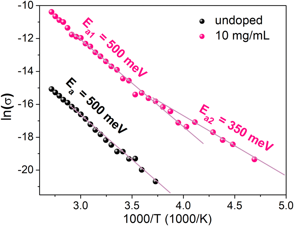 | ||
| Fig. 8 Temperature dependent conductivity of the undoped MAPI film and MAPI doped with 10 mg mL−1 SmI2. | ||
To confirm that the dopant freeze-out can explain both the low charge carrier density measured using the Mott–Schottky method and the occurrence of two distinguishable transport mechanisms observed in the temperature dependent conductivity measurements, charge transport simulations were carried out. Mott–Schottky plots of the sample exhibiting the highest conductivity (10 mg mL−1) were simulated for different donor energies, using the experimental data for Ea2 = 350 meV. The simulations were carried out using a small signal drift diffusion solver41 and ionic transport parameters (concentration and mobility) reported elsewhere42–44 (Table S2, ESI†). Ionized dopant density values (N+d) extracted from the simulated plots are plotted against the doping concentration Nd determined using XPS measurements (Fig. 9). As Ea decreases, the values of the ionized dopant density approach the values of the dopant concentration (until both values are the same for Ea = 0 eV, shown by the dashed line). Probing the value of Nd ≈ 1020 cm−3, one finds that the corresponding value of N+d for Ea = 350 meV is indeed ∼1017 cm−3, which is in agreement with the findings of the Mott–Schottky analysis. This confirms that the dopant freeze-out can indeed be the reason of the low level of the ionized dopant at room temperature. Moreover, simulations performed on the capacitor structure were used to convert the ionized impurities N+d extracted from the Mott Schottky analysis into a physical dopant concentration Nd (see Fig. S17 and Table S1 in the ESI†).
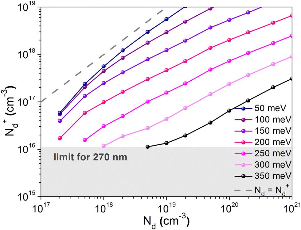 | ||
| Fig. 9 Impact of the dopant energy level Ed on the ionized dopant concentration extracted from the simulated 1/C2 plot versus the real dopant concentration. Ed is varying from 50 meV to 350 meV to highlight the effect of the dopant energy level Ed on the charge carrier density. Ed = 350 meV has been determined with conductivity versus temperature measurements. | ||
4. Conclusions
We demonstrate that n-type doping can be achieved by the incorporation of Sm2+ into MHPs, followed by its oxidation to Sm3+. The release of an electron during oxidation is the direct reason for the n-type of majority charge carriers. A shift of EF by 0.52 eV towards EC was deduced from the UPS measurement for 10 mg/ mL−1 dopant concentration. The ionized dopant density, measured using the Mott–Schottky method, showed this to be at a level of 1017 cm−3 for the 10 mg mL−1 dopant concentration, which is around 3 orders of magnitude lower than the dopant concentration value measured by depth-resolved XPS. This discrepancy is shown to be probably due to dopant freeze-out at RT due to a relatively high donor level Ea.The increase of charge carrier density is the reason for the increase in conductivity by ca. 3 orders of magnitude upon using Sm2+ ions as the dopant, in contrast to the use of Sm3+ that showed no change in conductivity. In spite of the modification of the surface morphology resulting from the doping process, the MHP crystal structure was preserved as shown by XRD. The proposed approach for perovskite doping appears promising and easy to be implemented in devices such as solar cells, LEDs, transistors, etc. While the main bottleneck of the presented example seems to be high dopant activation energy, it is believed that the ionization rate of the dopant can be enhanced by optimizing the perovskite formulation and/or the choice of the metastable divalent ions.
Author contributions
D. M. B. and L. H. had the idea to use metastable ions for doping. Z. M. and D. M. B. chose the suitable dopant and Z. M. developed a two-step doping method. Z. M. fabricated the samples, performed the measurements of conductivity, AFM, XRD, UV-Vis absorption, Mott–Schottky method, surface potential and temperature-dependent conductivity, analysed the data of all the performed experiments and wrote the draft of this article. B. P. performed the simulation of Mott–Schottky plots for different Ea and the sample thickness. Together with R. C., they wrote the conclusion on this part. M. A. guided the UPS analyses. S. C., D. M. B. and L. H. supervised the project and helped with writing.Conflicts of interest
There are no conflicts to declare.Acknowledgements
The Agence Nationale de la Recherche (HYPERSOL project no. ANR-18-CE05-0021-01) and the Region Nouvelle Aquitaine (STRIPE project no. 2019-1R1M08) are gratefully acknowledged for their financial support. XPS, SEM and TOF-SIMS analyses were made with the PLACAMAT facility with the fruitful help of C. Labrugère-Sarroste, P. Legros, N. Cam and JP. Salvetat. UPS analyses were made with the ELORPrintTec facility with the help of R. Lefèvre. The authors are grateful to Pr. Antoine Kahn (Princeton University) for fruitful discussions about the methodology for analyzing the UPS spectra.References
- T. M. Brenner, D. A. Egger, L. Kronik, G. Hodes and D. Cahen, Nat. Rev. Mater., 2016, 1, 1–16 CrossRef.
- A. Fakharuddin, L. Schmidt-Mende, G. Garcia-Belmonte, R. Jose and I. Mora-Sero, Adv. Energy Mater., 2017, 7, 1700623 CrossRef.
- M. A. Haque, D. Rosas Villalva, L. H. Hernandez, R. Tounesi, S. Jang and D. Baran, Chem. Mater., 2021, 33, 8147–8172 CrossRef CAS.
- A. L. Abdelhady, M. I. Saidaminov, B. Murali, V. Adinolfi, O. Voznyy, K. Katsiev, E. Alarousu, R. Comin, I. Dursun, L. Sinatra, E. H. Sargent, O. F. Mohammed and O. M. Bakr, J. Phys. Chem. Lett., 2016, 7, 295–301 CrossRef CAS PubMed.
- J. Euvrard, Y. Yan and D. B. Mitzi, Nat. Rev. Mater., 2021, 6, 531–549 CrossRef CAS.
- S. Heo, K. Roh, F. Zhang, S. E. Tignor, A. B. Bocarsly, A. Kahn and B. P. Rand, ACS Energy Lett., 2022, 7, 211–216 CrossRef CAS.
- J. Euvrard, O. Gunawan, X. Zhong, S. P. Harvey, A. Kahn and D. B. Mitzi, Mater. Adv., 2021, 2, 2956–2965 RSC.
- S. Sadhu, K. Aqueche, T. Buffeteau, J. M. Vincent, L. Hirsch and D. M. Bassani, Mater. Horiz., 2019, 6, 192–197 RSC.
- J. Zhang, M. Shang, P. Wang, X. Huang, J. Xu, Z. Hu, Y. Zhu and L. Han, ACS Energy Lett., 2016, 1, 535–541 CrossRef CAS.
- Y. Han, H. Zhao, C. Duan, S. Yang, Z. Yang, Z. Liu and S. Liu, Adv. Funct. Mater., 2020, 30, 1909972 CrossRef CAS.
- Y. Zhang, C.-C. Zhang, C.-H. Gao, M. Li, X.-J. Ma, Z.-K. Wang and L.-S. Liao, Sol. RRL, 2019, 3, 1800269 CrossRef.
- K. Arashiba, R. Kanega, Y. Himeda and Y. Nishibayashi, Chem. Lett., 2020, 49, 1171–1173 CrossRef CAS.
- T. Wang, K. C. Pitike, Y. Yuan, S. M. Nakhmanson, V. Gopalan and B. Jalan, APL Mater., 2016, 4, 126111 CrossRef.
- B. Y. R. D. Shannon, N. H. Baur, O. H. Gibbs, M. Eu and V. Cu, Acta Cryst., 1976, A32, 751–767 CrossRef.
- M. Szostak and D. J. Procter, Angew. Chem., Int. Ed., 2012, 51, 9238–9256 CrossRef CAS PubMed.
- P. Girard, J. L. Namy and B. Kagan, J. Am. Chem. Soc., 1980, 102, 2693–2698 CrossRef CAS.
- M. Szostak, M. Spain and D. J. Procter, J. Org. Chem., 2014, 79, 2522–2537 CrossRef CAS PubMed.
- W. J. Mir, T. Sheikh, H. Arfin, Z. Xia and A. Nag, NPG Asia Mater., 2020, 12, 9 CrossRef CAS.
- R. Sun, P. Lu, D. Zhou, W. Xu, N. Ding, H. Shao, Y. Zhang, D. Li, N. Wang, X. Zhuang, B. Dong, X. Bai and H. Song, ACS Energy Lett., 2020, 5, 2131–2139 CrossRef CAS.
- J. V. Patil, S. S. Mali and C. K. Hong, ACS Sustainable Chem. Eng., 2020, 8, 16364–16371 CrossRef CAS.
- W.-J. Yin, T. Shi and Y. Yan, Appl. Phys. Lett., 2014, 104, 63903 CrossRef.
- N. K. Noel, S. N. Habisreutinger, A. Pellaroque, F. Pulvirenti, B. Wenger, F. Zhang, Y. H. Lin, O. G. Reid, J. Leisen, Y. Zhang, S. Barlow, S. R. Marder, A. Kahn, H. J. Snaith, C. B. Arnold and B. P. Rand, Energy Environ. Sci., 2019, 12, 3063–3073 RSC.
- J. Euvrard, O. Gunawan and D. B. Mitzi, Adv. Energy Mater., 2021, 2, 2956–2965 CAS.
- G. Krill, A. Amamou and J. P. Senateur, J. Phys. F: Met. Phys., 1980, 10, 1889–1897 CrossRef CAS.
- Y. Mori, S. Tanemura, S. Koide, Y. Senzaki, P. Jin, K. Kaneko, A. Terai and N. Nabotova-Gabin, Appl. Surf. Sci., 2003, 212–213, 38–42 CrossRef CAS.
- J. A. Chang, J. H. Rhee, S. H. Im, Y. H. Lee, H. J. Kim, S. Il Seok, M. K. Nazeeruddin and M. Gratzel, Nano Lett., 2010, 10, 2609–2612 CrossRef CAS PubMed.
- C. Jiang, S. L. Lim, W. P. Goh, F. X. Wei and J. Zhang, ACS Appl. Mater. Interfaces, 2015, 7, 24726–24732 CrossRef CAS PubMed.
- F. Zhang, S. H. Silver, N. K. Noel, F. Ullrich, B. P. Rand and A. Kahn, Adv. Energy Mater., 2020, 10, 1–7 CrossRef PubMed.
- F. Zhang, F. Ullrich, S. Silver, R. A. Kerner, B. P. Rand and A. Kahn, J. Phys. Chem. Lett., 2019, 10, 890–896 CrossRef CAS PubMed.
- Y. F. Chen, Y. T. Tsai, D. M. Bassani, R. Clerc, D. Forgács, H. J. Bolink, M. Wussler, W. Jaegermann, G. Wantz and L. Hirsch, J. Mater. Chem. A, 2016, 4, 17529–17536 RSC.
- S. M. Sze, Y. Li and K. K. Ng, Physics of Semiconductor Devices, Wiley, 2021 Search PubMed.
- O. Almora, C. Aranda, I. Zarazua, A. Guerrero and G. Garcia-Belmonte, ACS Energy Lett., 2016, 1, 209–215 CrossRef CAS.
- T. Pang, K. Sun, Y. Wang, S. Luan, Y. Zhang, Y. Zhu, Z. Hu and R. Jia, J. Mater. Chem. C, 2020, 8, 1962–1971 RSC.
- G. Garcia-Belmonte and J. Bisquert, ACS Energy Lett., 2016, 1, 683–688 CrossRef CAS.
- O. Almora, C. Aranda, E. Mas-Marzá and G. Garcia-Belmonte, Appl. Phys. Lett., 2016, 109, 173903 CrossRef.
- T. Kirchartz, W. Gong, S. A. Hawks, T. Agostinelli, R. C. I. MacKenzie, Y. Yang and J. Nelson, J. Phys. Chem. C, 2012, 116, 7672–7680 CrossRef CAS.
- J. Siekmann, S. Ravishankar and T. Kirchartz, ACS Energy Lett., 2021, 6, 3244–3251 CrossRef CAS.
- S. Ravishankar, T. Unold and T. Kirchartz, Science, 2021, 371, eabd8014 CrossRef CAS PubMed.
- L. Hirsch and A.-S. Barriere, J. Appl. Phys., 2003, 94, 5014–5020 CrossRef CAS.
- P. Bouillon and T. Skotnicki, IEEE Electron Device Lett., 1998, 19, 19–22 CAS.
- M. T. Neukom, A. Schiller, S. Züfle, E. Knapp, J. Ávila, D. Pérez-del-Rey, C. Dreessen, K. P. S. Zanoni, M. Sessolo, H. J. Bolink and others, ACS Appl. Mater. Interfaces, 2019, 11, 23320–23328 CrossRef CAS.
- M. H. Futscher, M. K. Gangishetty, D. N. Congreve and B. Ehrler, J. Chem. Phys., 2020, 152, 44202 CrossRef CAS PubMed.
- J. Thiesbrummel, V. M. Le Corre, F. Peña-Camargo, L. Perdigón-Toro, F. Lang, F. Yang, M. Grischek, E. Gutierrez-Partida, J. Warby, M. D. Farrar and others, Adv. Energy Mater., 2021, 11, 2101447 CrossRef CAS.
- V. M. Le Corre, J. Diekmann, F. Peña-Camargo, J. Thiesbrummel, N. Tokmoldin, E. Gutierrez-Partida, K. P. Peters, L. Perdigón-Toro, M. H. Futscher, F. Lang and others, Sol. RRL, 2022, 6, 2100772 CrossRef CAS.
Footnote |
| † Electronic supplementary information (ESI) available. See DOI: https://doi.org/10.1039/d3mh00663h |
| This journal is © The Royal Society of Chemistry 2023 |