
 Open Access Article
 This Open Access Article is licensed under a
 Creative Commons Attribution 3.0 Unported Licence
Abnormal in-plane epitaxy and formation mechanism of vertically aligned Au nanopillars in self-assembled CeO2–Au metamaterial systems†
Juanjuan
Lu
 a,
Di
Zhang
ab,
Robynne L.
Paldi
a,
Zihao
He
c,
Ping
Lu
d,
Julia
Deitz
d,
Ahmad
Ahmad
a,
Hongyi
Dou
a,
Xuejing
Wang
a,
Juncheng
Liu
a,
Zedong
Hu
a,
Bo
Yang
a,
Xinghang
Zhang
a,
Anter A
El-Azab
a and
Haiyan
Wang
*ac
a,
Di
Zhang
ab,
Robynne L.
Paldi
a,
Zihao
He
c,
Ping
Lu
d,
Julia
Deitz
d,
Ahmad
Ahmad
a,
Hongyi
Dou
a,
Xuejing
Wang
a,
Juncheng
Liu
a,
Zedong
Hu
a,
Bo
Yang
a,
Xinghang
Zhang
a,
Anter A
El-Azab
a and
Haiyan
Wang
*ac
aSchool of Materials Engineering, Purdue University, West Lafayette, Indiana 47907, USA
bCenter for Integrated Nanotechnologies (CINT), Los Alamos National Laboratory, Los Alamos, NM 87545, USA
cSchool of Electrical and Computer Engineering, Purdue University, West Lafayette, Indiana 47907, USA
dSandia National Laboratories, Albuquerque, NM 87185, USA. E-mail: hwang00@purdue.edu
First published on 19th May 2023
Abstract
Metamaterials present great potential in the applications of solar cells and nanophotonics, such as super lenses and other meta devices, owing to their superior optical properties. In particular, hyperbolic metamaterials (HMMs) with exceptional optical anisotropy offer improved manipulation of light–matter interactions as well as a divergence in the density of states and thus show enhanced performances in related fields. Recently, the emerging field of oxide–metal vertically aligned nanocomposites (VANs) suggests a new approach to realize HMMs with flexible microstructural modulations. In this work, a new oxide–metal metamaterial system, CeO2–Au, has been demonstrated with variable Au phase morphologies from nanoparticle-in-matrix (PIM), nanoantenna-in-matrix, to VAN. The effective morphology tuning through deposition background pressure, and the corresponding highly tunable optical performance of three distinctive morphologies, were systematically explored and analyzed. A hyperbolic dispersion at high wavelength has been confirmed in the nano-antenna CeO2–Au thin film, proving this system as a promising candidate for HMM applications. More interestingly, a new and abnormal in-plane epitaxy of Au nanopillars following the large mismatched CeO2 matrix instead of the well-matched SrTiO3 substrate, was discovered. Additionally, the tilting angle of Au nanopillars, α, has been found to be a quantitative measure of the balance between kinetics and thermodynamics during the depositions of VANs. All these findings provide valuable information in the understanding of the VAN formation mechanisms and related morphology tuning.
New conceptsAs a newly emerged metamaterial system, oxide–metal vertically aligned nanocomposites (VANs) benefit from single-step self-assembled growth and a highly anisotropic nanostructure which enables strong enhancement in hyperbolic responses. However the lack of fundamental understanding over the formation mechanism and tuning rules of optical responses is limiting its broad applications. Here, we present an in-depth study into the growth mechanism through an intriguing VAN system of CeO2–Au, with an unexpected 45° in-plane rotation of Au lattices on SrTiO3 substrate despite a nearly perfect lattice match. Three distinguishable morphologies have been explored via tuning oxygen background pressure. The tilting angle of nanopillars, α, has been first proposed as a quantitative measure of the balance between kinetics and thermodynamics during deposition. VAN morphology has thus been proven to be a kinetics-dominant growth, which provides valuable information in future nanostructure designs. Effective tuning of localized plasmonic resonance (LSPR) via morphology modulation is realized, and the nano-antenna sample presents Type I hyperbolic properties. Extensive COMSOL simulation confirmed the importance of shapes, density, distributions, and tilting of nanoinclusions in an enhanced LSPR effect. This work provides essential understanding for nanoscale metamaterial designs and addresses the needs of versatile morphologies towards advanced optics and plasmonic applications. |
Introduction
Metamaterials are artificially engineered materials with a three-dimensional repetitive arrangement of certain subwavelength-scale components, designed to achieve unconventional electromagnetic functionalities that are not existent or comparable in any of their components.1,2 Exceptional optical properties such as negative refraction index,3 optical nonlinearity,4 hyperbolic pagations,5etc.6,7 are typical in metamaterials due to the excitation of surface plasmon polaritons (SPPs)8 and localized surface plasmons (LSPs)9 upon incident illumination, taking advantage of the localized oscillation of charge carriers.10 Their corresponding applications include optical cloaking,11 energy harvesting,12,13 holography,4 nanophotonics,14–16 photovoltaics,17 and so on.18,19 As an alternative approach to the traditional tedious fabrication methods such as electron beam lithography20 and anodic aluminum oxide (AAO) template assisted growth,21 self-assembled oxide–metal vertically aligned nanocomposites (VANs) have attracted extensive interest in many research areas due to the ease in assembling this pulsed laser deposition (PLD) based nanopillar-in-matrix thin film morphology, as well as reliable vertical growth and uniform distribution of metallic nanopillars embedded in the oxide matrix. Specifically, when plasmonic metals such as Au, Ag and Cu are included in the VAN systems, for example, BaTiO3–Au,22,23 BaTiO3–AuAg,24 ZnO–Au,25 La0.7Sr0.3MnO3–Au,26,27 ZnO–Cu,28etc.,29,30 most of them exhibit an extremely dispersive optical response named hyperbolic metamaterials (HMMs) characteristic due to the enhancement of LSPs, which is promising especially for advanced optical and imaging applications.5,21,31 Most HMMs are composite material systems with uniaxial anisotropy, where one or two of the three components (x-, y- and z-axis vector components) are negative and the others are positive.5 The key to achieving HMM lies in the manipulation of surface plasmons, which relies primarily on the tuning of the morphologies and interfaces between metals and dielectrics.32,33 From this perspective, VAN structures are known to have the advantages of being easily manipulated by PLD deposition parameters such as laser pulse numbers,23 substrate temperature,34 laser frequency,35 background atmosphere,25etc.Although related VAN growth studies have emerged in recent years, an in-depth understanding of the formation mechanism as well as the microstructural tuning principles for PLD-based VANs is still lacking. Overall, challenges remain in the following aspects: (1) tuning of morphologies by multiple deposition parameters; (2) the interplays between the kinetic deposition process and thermodynamic considerations;36 and, (3) the competition between interfacial energy and elastic energy.37 Overall, the understanding of the growth mechanisms for oxide–metal VANs is very much needed for better designs and growth of oxide-metal VAN systems.
In this work, a newly designed two-phase oxide-metal VAN system, CeO2–Au, was fabricated with highly distinctive Au phase morphologies achieved by tuning deposition oxygen background pressure. The experimental design of this work is summarized in Fig. 1. CeO2, Au and SrTiO3 are selected first to satisfy a strain compensation model toward a desired VAN morphology.38 Furthermore, the background oxygen pressure during deposition (200 mTorr, 50 mTorr and vacuum) has been explored for tuning the Au nanostructure morphologies in this hybrid system, as illustrated in the schematic drawings in Fig. 1. Unexpectedly, this system has presented an abnormal epitaxial relationship that has never been reported before, which at the same time, suggests some updates to the underlying formation theories for oxide–metal VAN morphology. The morphology change in this work is also accompanied by tunable optical responses, such as the plasmonic wavelength ranges, and hyperbolic dispersions, which will be demonstrated by ellipsometry and optical transmittance measurements in the discussion part. This structural and optical property tuning in the CeO2–Au metamaterial system not only presents its importance in the study of VAN formation rules, but also shows its potential as a HMM candidate in future optical device integrations.
 | ||
| Fig. 1 Illustration of the experimental designs. Au nanoinclusions are represented as yellow, the CeO2 matrix is coded by red and STO is aqua. As background oxygen pressure decreases, the Au morphology changes from nanopillar-in-matrix (PIM), nanoantenna-in-matrix, to vertically aligned nanocomposites (VAN). (a) The CeO2–Au film deposited under 200 mTorr oxygen with PIM morphology; (b) the CeO2–Au film deposited under 50 mTorr oxygen with a nanoantenna-in-matrix morphology; (c) the CeO2–Au film deposited under ultra-high vacuum (UHV) with VAN morphology. Note that the in-plane ordered Au nanoinclusions are for illustration purpose. | ||
Results and discussion
2.1. Structural characterization
 after in-plane rotation) and Au (FCC, a =4.079 Å) on a SrTiO3 (STO) (perovskite structure, a =3.905 Å) substrate allows the strain compensation model to be effective. To satisfy epitaxial growth, it is expected that CeO2 will present a 45° in-plane rotation with STO,39 while Au will match with STO with a cube-on-cube relationship, as illustrated in Fig. S1 (ESI†). We thus use phi scan, and transmission electron microscopy (TEM) plan-view and cross-section analysis to confirm the actual orientation relationships. Upon depositions of CeO2–Au nanocomposite samples, X-ray diffraction (XRD) θ/2θ scans were first performed to investigate the crystallinity and epitaxial quality of the films. As shown in Fig. S2 (ESI†), all XRD patterns demonstrate great crystallinity and highly textured growth of CeO2–Au nanocomposite films. The out-of-plane (OP) growth orientation for all films remain the same as Au(002)//CeO2(002)//STO(002). Fig. S2(b) and (c) (ESI†) are the enlarged area of Fig. S2(a) (ESI†) with a 2θ range of 25–40° and 35–50°, respectively. Compare CeO2(002) and Au(002) peak locations to the bulk values in the PDF card, all three CeO2–Au samples deposited under 200 mTorr, 50 mTorr and vacuum, present little or no obvious lattice strain. This demonstrates smooth film growth with minimum strain. However, as the partial pressure increases from ultra-high vacuum (UHV) to 200 mTorr, the decrease of CeO2(002) peak intensity indicates the deterioration of film crystallinity. This has also been reported in other oxide-metal nanocomposite systems such as ZnO–Au.25
Following the XRD measurement, cross-sectional TEM and scanning transmission electron microscopy (STEM) imaging along with energy-dispersive X-ray spectroscopy (EDS) mapping were taken for all three sets of samples deposited under 200 mTorr, 50 mTorr and vacuum, as shown in Fig. 2(a–i). Fig. 2(a–c) are the STEM and EDS images of the 200 mTorr oxygen grown film. This film has an average thickness of 57.76 nm. In this film, all Au nanoinclusions grow as isolated nanoparticles randomly dispersed throughout the film thickness. According to Fig. 2(a), the average size of nanoparticles in this sample is approximately 5.61 ± 2.00 nm, demonstrating a large diameter variance. Notably, the matrix phase CeO2 shows a columnar growth instead of a continuous layer for a thickness beyond ∼12 nm under 200 mTorr.40 This suggests that this film has a larger porosity than other samples. Metallic nanoparticles are thus sandwiched in between neighbouring columns for the top part of this film. When decreasing the background pressure to 50 mTorr, Au nanoparticles in the film start to gather and assemble into pillar-shaped aggregations, as demonstrated in Fig. 2(d–f). This film presents an obvious sectional growth, with the first layer as the nucleation layer, the second layer as a fishnet-resembling connecting sideway-tilted nanopillars, and the top layer still as nanoparticle-in-matrix morphology. Despite the morphology change across the entire thickness, this sample appears to be distinctive from either the PIM sample in Fig. 2(a–c) or the VAN sample in Fig. 2(g–i). In the top layer, the nanoparticles tend to be elongated to connect to the neighbour nanostructures. In the bottom nucleation layer, the vertical growth of short nanopillars does not last for more than ∼12 nm before tilting sideways and reaching out to the adjacent nanoinclusions. Because this sample has the typical symmetrically tilted connection of Au nanoinclusions, different from either the PIM or VAN samples, this morphology is referred as “nano-antenna” in the following discussion. Thus, Fig. 1(b) is a typical illustration of this special nanostructure. Additionally, comparing Fig. 2(f) to Fig. 2(c), there is a somewhat similar angle for this tilted connection. From Fig. 2(d) and (f), the tilting angles of nano-inclusions in the second layer were defined as α and measured as averagely ∼53.6°, with a deviation of 1.6°. For better visualization, an additional set of STEM and EDS images from a thinner area is shown in Fig. 3(a) and Fig. S3 (ESI†). Note that the nanoparticle-in-matrix nanostructure in the right part of this figure does not represent the overall morphology of this sample, because this is the thin area damaged by an ion milling process during the sample preparation. And, due to the projection effect, the angle measured from cross-sectional TEM images may be slightly larger. But the error should be limited according to the uniformity of contrast in STEM images and the lattice continuity from HRSTEM images shown in Fig. 3(b). The thickness values for these three regions are ∼11.3 nm for the bottom nucleation layer, ∼107.0 nm for the middle nanoantenna layer, and ∼23.8 nm for the top particle-in-matrix layer, giving this nanoantenna structure a total thickness of ∼141.4 nm. Finally, as background oxygen partial pressure was decreased to vacuum (∼1 × 10⁻⁶ mTorr), a typical VAN morphology with Au nanopillars grown slightly tilted at the top of the film is demonstrated by Fig. 2(g–i). The initial ∼27.6 nm growth is a vertical growth from the substrate surface, but in the following ∼60.1 nm thickness, however, the pillar tends to tilt at small angles, as shown by the dashed outliners in Fig. 2(i). The average tilting angle α in this sample is measured to be ∼62.6°. Especially, Fig. 2(g) shows that there is not only a gradual change in the tilting angles, but also different tilting directions for some of the pillars. This gradual modification of tilting angle α in CeO2–Au systems grown under different background pressure will be further discussed in the following sub-section. Surface roughness of the three samples was determined by atomic force microscopy (AFM). Their 2D mappings and 3D mapping results are shown in Fig. S4 (ESI†). The average surface roughness for the PIM sample, the nanoantenna sample, and the VAN sample are 34.7 ± 3.36 nm, 16.0 ± 2.0 nm and 9.0 ± 1.3 nm, respectively. This indicates an obviously reduced surface roughness as the background atmosphere pressure drops. Additionally, to further verify these assumptions made concerning the three sets of CeO2–Au samples fabricated under vacuum, 50 mTorr and 200 mTorr, two other CeO2–Au samples were deposited under 100 mTorr and 150 mTorr oxygen background pressure. Their morphologies are shown in Fig. S5 and S6 (ESI†). The microstructures of 100 mTorr and 150 mTorr samples appear to be clear transition states from the nanoantenna sample to the PIM sample demonstrated in Fig. 2(a–f), including the Au nanoinclusion morphology, CeO2 quality, and the surface roughness. Overall, the CeO2–Au nanocomposite thin film nanostructure is effectively modulated by the background oxygen pressure. Three distinguishable morphologies are discovered as oxygen pressure decreases: nanoparticle-in-matrix, nanoantenna-in-matrix, and vertically aligned nanopillars-in-matrix.
 | ||
| Fig. 2 STEM and EDS images showing the cross-sectional microstructure development in three sets of CeO2–Au thin films. (a), (d) and (g) are the STEM images. (b and c), (e and f) and (h and i) are the EDS images from the enlarged areas in the corresponding STEM images. (a)–(c) show the PIM sample that was deposited under 200 mTorr background oxygen pressure. (d–f) show the three-phase growth of the nanoantenna sample that was fabricated under 50 mTorr background oxygen pressure. And (g–i) shows the slightly tilted VAN growth of Au nanopillars when depositing in vacuum. In particular, the vertical growth height of Au nanopillars and tilting angles are denoted in (d) and (g). | ||
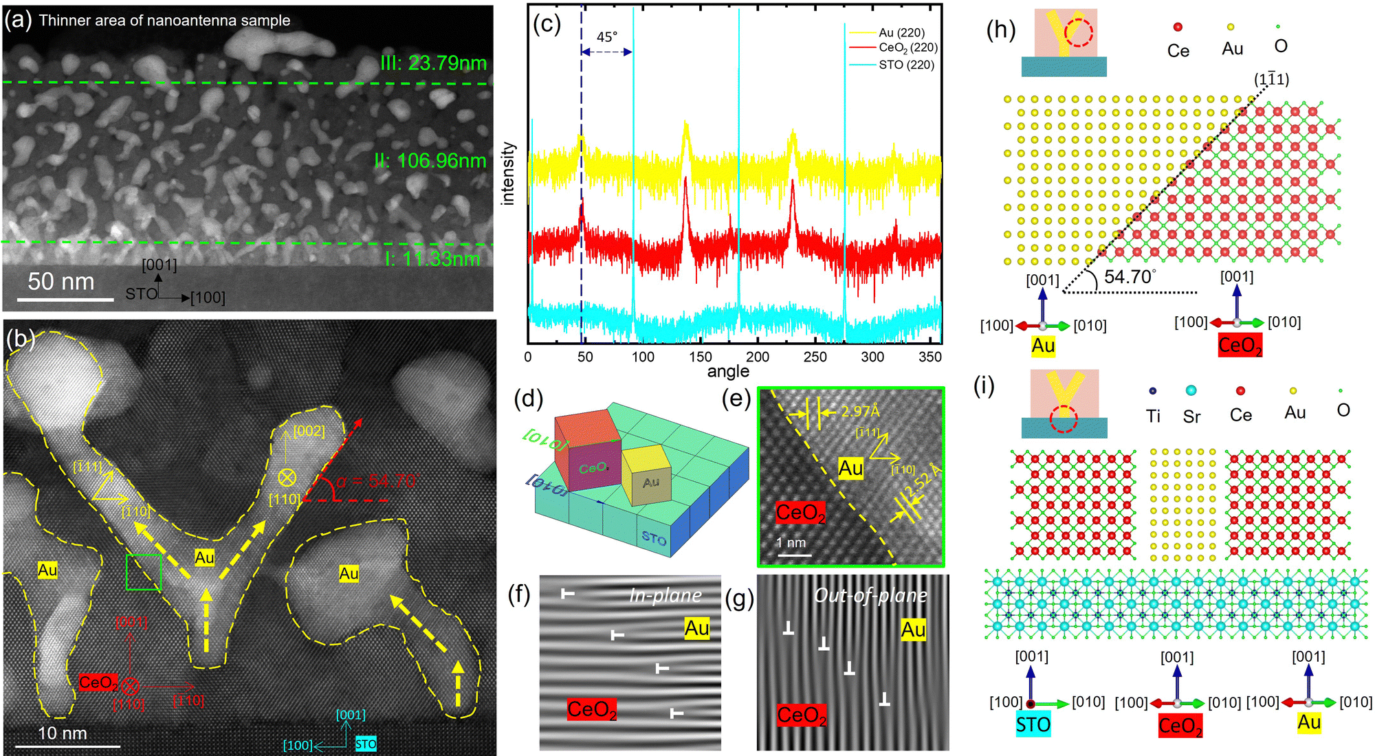 | ||
Fig. 3 HRSTEM images of the nanoantenna CeO2–Au thin film and the epitaxy analysis. (a) A low-magnification STEM image showing the three growth phases of the nanoantenna sample in a thinner area of the sample. The distinctive three growth phases are denoted as I, II, and III in green. (b) HRSTEM image of the nanoantenna thin film showing the first and second stages of Au growth. Angle α demonstrates the tilting of Au. (c) is the X-ray phi scan result of (220) planes in Au, CeO2 and STO. (d) is an illustration of the abnormal in-plane epitaxy of CeO2 and Au lattices on top of the STO substrate. (e) is the enlarged area in (b) along with the respective (f) in-plane and (g) out-of-plane inversed FFT images. 3.07 Å and 2.60 Å are the d-spacing values of (110) and (111) planes, compared to bulk values of 2.88 Å and 2.36 Å. (h) shows the tilted interfaces in (b), as denoted by the inset 2D intersection illustration on the bottom left, and (i) is a demonstration of the vertical interfaces. The contacting interface appears to be (11![[1 with combining macron]](https://www.rsc.org/images/entities/char_0031_0304.gif) ). ). | ||
The growth mechanism of a typical oxide-metal VAN system mainly includes three steps22: (1) adatoms arrive at the substrate surface and undergo a diffusion process; (2) the metallic adatoms nucleate following a 3D Volmer–Weber island growth mode, while the oxide matrix phase starts the growth in a 2D Frank-van der Merve mode or a mixed 2D + 3D Stranski–Krastanov mode; (3) the continuous film growth by adatoms agglomeration of the same species. In the case of CeO2–Au VAN systems, the tailorable morphology by a background atmosphere as summarized above can be explained as a tuning of kinetics in the first step, i.e., the change in the adatoms diffusion process: By increasing the oxygen background pressure, it results in more confined plasma plume, and thus a decreased mean free path of adatoms and reduced energy for the following adatoms nucleation and growth process.41 Consequently, the diffusion of adatoms on the substrate surface is restricted as the oxygen pressure gets elevated, giving rise to a more thermodynamics-dominated growth. This results in the nanoantenna or PIM morphology. Furthermore, as the plume is more confined by increasing the background pressure, a lowered film thickness and an increased surface roughness can also be expected. All of these correspond to the experimental observations as mentioned above. Note that the thickness of the VAN sample in this case is smaller than the nanoantenna sample, which should be attributed to the tilted angle of Au nanopillars, α. This will be elaborated further in Section 2.1.3.
In conclusion, the background atmosphere during the PLD depositions is a powerful parameter for the modulation of morphology during the CeO2–Au deposition, which is consistent with previous reports.25 Furthermore, it is proposed that the unique VAN morphology of oxide-metal nanocomposites should be considered as a kinetics-dominated result.
![[2 with combining macron]](https://www.rsc.org/images/entities/char_0032_0304.gif) 20)//CeO2 (20)//STO(020) from the in-plane direction. The 45° rotated matching between CeO2 and STO is verified from this epitaxial relationship. However, it is interesting to note that Au has the same 45° in-plane rotated orientation as the CeO2 matrix, exposing (110) planes from the out-of-plane direction. Instead of aligning (010) planes with STO(010) planes from the IP direction as a consequence of the substrate clamping effect, Au lattices selected an abnormally preferred IP matching based on the CeO2 matrix lattices. This is the first time this kind of matrix-determined IP epitaxy relationship is observed in VAN systems. Fig. 3(d) is a 3D illustration of this lattice matching relationship. The [010] directions of CeO2 and STO lattices are shown by the arrows in the illustration, respectively. To understand the importance of strain caused by lattice mismatch among the three phases, all possible plane matching combinations and their corresponding misfit values were calculated and shown by Table S1 (ESI†). The green color-coded pairs are the observed lattice matching relationships in the CeO2–Au composite system described in this work. Considering a previously expected cube-on-cube IP epitaxy supported by the strain compensation model, Au(200)//CeO2(220)//STO(200), the misfit of CeO2/Au and Au/STO is 6.39% and −4.36%, respectively. When Au lattices select the 45° rotated IP orientation with domain matching epitaxy relationships of Au:STO = 4
20)//CeO2 (20)//STO(020) from the in-plane direction. The 45° rotated matching between CeO2 and STO is verified from this epitaxial relationship. However, it is interesting to note that Au has the same 45° in-plane rotated orientation as the CeO2 matrix, exposing (110) planes from the out-of-plane direction. Instead of aligning (010) planes with STO(010) planes from the IP direction as a consequence of the substrate clamping effect, Au lattices selected an abnormally preferred IP matching based on the CeO2 matrix lattices. This is the first time this kind of matrix-determined IP epitaxy relationship is observed in VAN systems. Fig. 3(d) is a 3D illustration of this lattice matching relationship. The [010] directions of CeO2 and STO lattices are shown by the arrows in the illustration, respectively. To understand the importance of strain caused by lattice mismatch among the three phases, all possible plane matching combinations and their corresponding misfit values were calculated and shown by Table S1 (ESI†). The green color-coded pairs are the observed lattice matching relationships in the CeO2–Au composite system described in this work. Considering a previously expected cube-on-cube IP epitaxy supported by the strain compensation model, Au(200)//CeO2(220)//STO(200), the misfit of CeO2/Au and Au/STO is 6.39% and −4.36%, respectively. When Au lattices select the 45° rotated IP orientation with domain matching epitaxy relationships of Au:STO = 4![[thin space (1/6-em)]](https://www.rsc.org/images/entities/char_2009.gif) :3 and Au:CeO2 = 4:3, the misfit values of CeO2/Au and Au/STO are reduced to 4.85% and 1.54%, respectively. Meanwhile, CeO2(110)//STO(001) is always preferred when the lattices are matched with the 45° in-plane rotation, which is common in all CeO2 films grown on a STO substrate.23,39,43 Moreover, it is noted from HRSTEM images of the nanoantenna sample that some of the Au nanoinclusions start their nucleation halfway from the CeO2 matrix, but not from the substrate surface. This is a phenomenon commonly seen in some of the VAN systems.44 This could have contributed partly to this anomalous Au IP orientation found in this case.
:3 domain matching epitaxy between the two phases. And the existence of dislocations is a demonstration of fully relaxed lattices at the interface. This corresponds to the XRD result in Fig. S2 (ESI†). Next, as discussed above, most Au nanoantennas in the second growth region have a tilting angle of 53.6 ± 1.6°. Specifically, for the Au nanoantenna in the middle of Fig. 3(b), α is measured to be exactly 54.7° for both Au branches tilting at opposite directions, which is the same angle between Au(111) and Au(110) planes in Au bulk lattices. Thus, a conclusion is drawn that Au(111) planes are exposed perfectly at CeO2/Au interfaces in this case, resulting in a tilting angle α = 54.7°. This is probably due to the fact that {111} planes have the lowest energy in face centered cubic (FCC) Au.45Fig. 3(h) is an atomic model illustration constructed using VESTA software,46 showing the contact angle of 54.7° at the Au(11)/CeO2(11) crystal plane interface. In contrast, the vertical part of Au nanopillars exposes Au(001) planes at the Au/CeO2 interface, as shown by the atomic model in Fig. 3(i). The domain matching of Au:CeO2 = 4:3 is also observed on the interfaces on both models. This is an intriguing finding since the tilting of Au nanoantennas is thus an experimental confirmation for a thermodynamically accommodated growth of Au nanoinclusions in the CeO2 matrix, i.e., a growth state in thermodynamical equilibrium, since the lowest energy {111} planes are exposed at the interfaces.47 Comparatively, the vertical growth of Au, is more of a result of the kinetics-controlled growth, because it is the opposite of the energetically preferred growth. Therefore, the variance of Au pillar tilting angle α, can be considered as a parameter related to the balance between kinetics and thermodynamics in the growth of CeO2–Au VAN systems. Based on the discussions above, the tilting angle α for CeO2–Au nanocomposite thin film systems should vary in the range of [54.7°, 90°]. When α = 90°, Au {001} planes are exposed at the CeO2/Au interfaces and the morphology of Au is a vertical nanopillar. With varying deposition parameters, an energetically favorable growth pattern can result in tilted Au nanopillars until Au {111} planes are exposed completely and α = 54.7°. In this sense, the divergence of tilting angle α from 53.6° in the nanoantenna sample to 62.6° in the top-tilted VAN sample can be used as a quantitative indicator of the balance between kinetics and thermodynamics during the deposition process of CeO2–Au nanocomposite films. α here is proposed in this work as a new quantitative measure for the thermodynamic-kinetic competition which determines the resulting morphology of the CeO2–Au nanocomposite system, and possibly in other VAN systems. This finding will not only help an in-depth understanding in the growth mechanisms, but also assist future microstructure engineering of VAN systems.
:3 and Au:CeO2 = 4:3, the misfit values of CeO2/Au and Au/STO are reduced to 4.85% and 1.54%, respectively. Meanwhile, CeO2(110)//STO(001) is always preferred when the lattices are matched with the 45° in-plane rotation, which is common in all CeO2 films grown on a STO substrate.23,39,43 Moreover, it is noted from HRSTEM images of the nanoantenna sample that some of the Au nanoinclusions start their nucleation halfway from the CeO2 matrix, but not from the substrate surface. This is a phenomenon commonly seen in some of the VAN systems.44 This could have contributed partly to this anomalous Au IP orientation found in this case.
:3 domain matching epitaxy between the two phases. And the existence of dislocations is a demonstration of fully relaxed lattices at the interface. This corresponds to the XRD result in Fig. S2 (ESI†). Next, as discussed above, most Au nanoantennas in the second growth region have a tilting angle of 53.6 ± 1.6°. Specifically, for the Au nanoantenna in the middle of Fig. 3(b), α is measured to be exactly 54.7° for both Au branches tilting at opposite directions, which is the same angle between Au(111) and Au(110) planes in Au bulk lattices. Thus, a conclusion is drawn that Au(111) planes are exposed perfectly at CeO2/Au interfaces in this case, resulting in a tilting angle α = 54.7°. This is probably due to the fact that {111} planes have the lowest energy in face centered cubic (FCC) Au.45Fig. 3(h) is an atomic model illustration constructed using VESTA software,46 showing the contact angle of 54.7° at the Au(11)/CeO2(11) crystal plane interface. In contrast, the vertical part of Au nanopillars exposes Au(001) planes at the Au/CeO2 interface, as shown by the atomic model in Fig. 3(i). The domain matching of Au:CeO2 = 4:3 is also observed on the interfaces on both models. This is an intriguing finding since the tilting of Au nanoantennas is thus an experimental confirmation for a thermodynamically accommodated growth of Au nanoinclusions in the CeO2 matrix, i.e., a growth state in thermodynamical equilibrium, since the lowest energy {111} planes are exposed at the interfaces.47 Comparatively, the vertical growth of Au, is more of a result of the kinetics-controlled growth, because it is the opposite of the energetically preferred growth. Therefore, the variance of Au pillar tilting angle α, can be considered as a parameter related to the balance between kinetics and thermodynamics in the growth of CeO2–Au VAN systems. Based on the discussions above, the tilting angle α for CeO2–Au nanocomposite thin film systems should vary in the range of [54.7°, 90°]. When α = 90°, Au {001} planes are exposed at the CeO2/Au interfaces and the morphology of Au is a vertical nanopillar. With varying deposition parameters, an energetically favorable growth pattern can result in tilted Au nanopillars until Au {111} planes are exposed completely and α = 54.7°. In this sense, the divergence of tilting angle α from 53.6° in the nanoantenna sample to 62.6° in the top-tilted VAN sample can be used as a quantitative indicator of the balance between kinetics and thermodynamics during the deposition process of CeO2–Au nanocomposite films. α here is proposed in this work as a new quantitative measure for the thermodynamic-kinetic competition which determines the resulting morphology of the CeO2–Au nanocomposite system, and possibly in other VAN systems. This finding will not only help an in-depth understanding in the growth mechanisms, but also assist future microstructure engineering of VAN systems.
 | ||
| Fig. 4 Plan-view STEM images of the tilted VAN sample. (a) A low magnification overview of the Au nanopillar distribution in the CeO2 matrix. Au nanopillars have obvious shape differences and there appears to be certain in-plane ordering along directions depicted in the figure. (b) and (c) HRSTEM images of vertical Au nanopillars from the plan-view direction with rectangular and circular shapes. The inset of (b) shows the square-shaped Au nanopillar. (d) HRSTEM image showing some of the tilted Au nanopillars from the plan-view direction. (e) Correlation function result based on (a). The ordering and shape preference of Au nanopillars are visually demonstrated by the color-coded probability. | ||
Most vertical pillars present a square plan-view shape with an IP epitaxy of Au(010)//CeO2(010), as demonstrated by the inset at the top of Fig. 5(b). However, there are two other major types of irregular pillars that occupy a small amount of Au nanopillars, i.e., rectangular (type II) and circular/elliptical (type III) shapes, as demonstrated in the HRSTEM images of Fig. 4(b) and (c). Fig. 4(b) shows a rectangular shaped pillar with an IP lattice matching of Au(011)//CeO2(010) and Au(100)//CeO2(100) at the two interfaces. This type of Au nanopillar has an OP growth direction of [110], different from the [001] direction in the square shaped Au nanopillars. However, it is interesting that no Au(010) planes were observed in the pillars from cross-sectional HRSTEM images. Since most Au pillars are tilted from the thickness of ∼28.13 nm, with some even from ∼14.38 nm according to Fig. 2(g–i), another possibility is that the halfway tilting of the pillars resulted in this distinct growth orientation. Either way, the presence of Au(110) planes from the OP direction explains the relatively strong XRD peak of Au(110), especially in the nanoantenna sample. Fig. 5(b) shows an intriguing fact in the rectangular-shaped Au nanopillars that the side exposing Au(001) planes is slightly longer than the side of Au(110) planes. They are both matched with CeO2 {010} planes. Notably, the Au(110) side has a curved interface to expose Au(111) planes as much as possible. In square shaped pillars, the four corners are also rounded, exposing (111) planes to be thermodynamically favorable. Therefore, the orientation of pillars has a significant impact on their IP shapes and alignment directions.
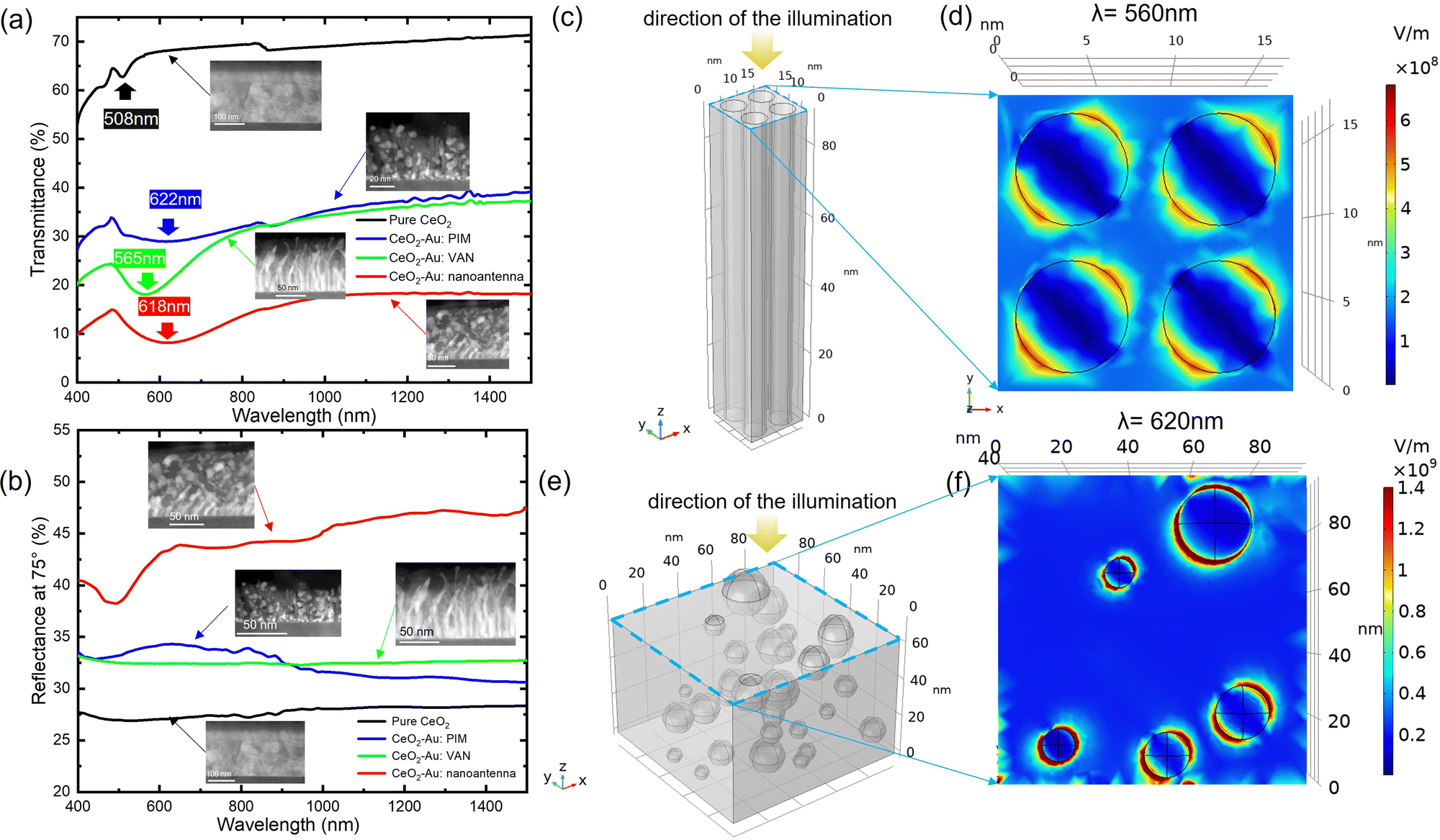 | ||
| Fig. 5 (a) The transmittance and (b) reflectance spectra for pure CeO2, CeO2–Au VAN, nanoantenna, and PIM samples. (c) is the geometrical model of the VAN sample based on the experimental results. It consists of four Au nanopillars embedded inside the CeO2 matrix. (d) is the corresponding electric field mapping (EFM) profile of the geometrical model (c) at an incident wavelength of 560 nm, showing the distribution of the electric field amplitude distribution in this model from the top view (XY plane). (e) Is the geometrical model of the PIM sample based on the experimental observations. The Au nanoparticle diameters, density, as well as the distribution locations are determined based on the cross-sectional and plan-view TEM images of the PIM sample. (f) Is the corresponding EFM profile for model (e) at an incident wavelength of 620 nm demonstrating the electric field amplitude distribution from the top view (XY plane). The dimensions of geometrical models can be derived from the parameters as described in the experimental section and the unit for the scale grid is nanometer. The change in colors from EFM demonstrates the difference in electric field amplitude. Red and blue colors imply a high and low |E/E0|2, respectively. Additionally, the EFM using a nanoantenna unit as an illustration for the nanoantenna CeO2–Au sample is shown in Fig. S12 (ESI†) for comparison. | ||
An interesting phenomenon is demonstrated in the type III pillar morphology, circular-shaped pillars by Fig. 4 (c), where the Au pillar lattice has a five-fold symmetry divided by (111) twin boundaries. This type of Au pillar has a growth orientation of [110], the same as the rectangular-shaped pillars described above. In Fig. 4(c), it can be observed that the Au lattices are divided into five domains in a standard pentagonal fashion, with an intersection angle of 72°. This twined domain pattern is possibly a typical demonstration of nanoscale rotational distortion defect in the FCC lattices, named disclination.48–50 The presence of pentagonal disclinations in Au nanopillars is believed to be a result of local elastic strain relaxation.49,51 Related demonstrations in VAN thin films are very rare,23 and this discovery suggests another possible mechanism for the strain relaxation in metallic pillars.
Additionally, to study the preference of the tilting direction, in Fig. 4(d), a selected area of Fig. 4(a) shows some of the tilted pillars that have rectangular and circular in-plane shapes. The tilting directions are denoted by the yellow-colored dashed arrows. Like the pillar shape, the tilting direction is also closely related to the orientations of pillars for the rectangular tilted pillars. They tend to tilt along CeO2 <100> directions, while circular pillars have relatively random tilting directions, as demonstrated by Fig. S8 (ESI†).
2.2. Optical properties
According to the discussion above, the selection of CeO2, Au, and STO is also related to the introduction of localized surface plasmon resonance (LSPR) effect and the HMM characteristics. First, as one of the most commonly used plasmonic metals, Au was selected as a LSPR mediator. The selected matrix material, CeO2, is a well-investigated oxide with excellent electronic and electrochemical catalytic properties as sensors52 and electronic devices.53 Furthermore, CeO2 has a positive permittivity around 26,54 which is almost exactly opposite to that of Au (about -45∼0 at the wavelength region of 400 nm∼1500 nm).55,56 The resulting CeO2–Au VAN is thus expected to have strong HMM characteristics.31A COMSOL electric field (|E/E0|2) map (EFM) simulation study was conducted to visually reveal the LSPR distribution near the metal–dielectric interfaces when the film is under the illumination of an electromagnetic wave at certain wavelength. After the construction of geometrical models (Fig. 5(c) and (e)) using the microstructural parameters obtained from TEM/STEM images, electric field amplitude profiles from the XY planes of the VAN and PIM composite structures are shown in Fig. 5(d) and (f). Fig. 5(d) is the top-view (XY plane) EFM amplitude profile of the VAN sample at an incident illumination wavelength of 560 nm. Fig. 5(f) is the corresponding EFM amplitude profile for the PIM sample from the XY plane, and the illumination wavelength is set to 620 nm. Additionally, the same simulation on the two samples was conducted at 1500 nm for comparisons, as shown in Fig. S11 (ESI†). The interaction between Au and CeO2 is more intense at the LSPR wavelength than the 1500 nm scenario, where little electron oscillation occurs. Comparing Fig. 5(d) to (f), the Au particle induces a much stronger electric field contrast, due to the higher curvatures of CeO2/Au interfaces.60 This explains the superior anisotropy of PIM and nanoantenna samples as discussed in the next section. In Fig. S13 (ESI†), another geometrical model was built with the same geometry parameters of the VAN sample and an additional tilting angle α of 62° around the z-axis, to investigate the influence of nanopillar tilting. The cross-sectional FEM amplitude profiles for XY and YZ planes at a wavelength λ = 560 nm is shown in Fig. S13(b) and (c) (ESI†). Note that the YZ plane cross-sectional FEM amplitude profile in Fig. S13(b) (ESI†) is located at the center of the nanopillars. The electric field enhancement at the Au nanopillar edges is surprisingly stronger in the tilted model, especially along the direction toward the tilting. Especially, the YZ plane EFM amplitude profile in Fig. S13(c) (ESI†) shows that the enhancement of the field extends deeper into the film in the case of tilted pillars. This suggests an intensified LSPR effect in the tilted pillars. Thus, this explains the deeper transmittance valleys of VAN and nanoantenna samples in Fig. 5(a). The LSPR excitation due to the incident light has a thickness limitation, and as the tilting angle α increases, the limitation gets weaker. In consequence, for the nanoantenna-structured thin film with a three-phase sectional growth, the electric field distribution in its top particle-growth layer should resemble the PIM model. This corresponds to the similar transmittance dip locations of nanoantenna and PIM samples in Fig. 5. Furthermore, for the nanoantenna sample, despite the difficulties in determining the exact structural parameters, an illustration of the COMSOL model is demonstrated in Fig. S12 (ESI†). Strong electric field enhancement is found at places where nanoinclusions are located more closely. This explains why the nanoantenna sample has the most divergent optical responses as discussed in Section 2.2.2.
 | ||
| Fig. 6 Real and imaginary permittivity from in-plane (IP) and out-of-plane (OP) directions retrieved from ellipsometry measurement: (a) and (b) the PIM sample, (c) and (d) the nanoantenna sample, (e) and (f) the VAN sample. (a), (c) and (e) are the real permittivity for the three samples, and (b), (d) and (f) show their corresponding imaginary permittivity. The inset illustrations in the imaginary permittivity graphs demonstrate the measurement settings: linearly polarized incident light is illuminated onto the film surface, and the spectra detector collects the resultant elliptically polarized reflected light signals. The film morphologies are indicated for the three sets of films, respectively. IP and OP are the directions along and vertical to the film surfaces. | ||
First, it is interesting that the dielectric permittivity values of all CeO2–Au samples in the measured wavelength region are much smaller than that of pure CeO2 films, which is ∼26.54 Especially for the nanoantenna sample, the sudden increase in Im(ε‖) and Im(ε⊥) at a wavelength larger than 514 nm indicates the enhancement of plasmonic resonance, which corresponds to the dips in reflectance and transmittance graphs in Fig. 5. In all samples, the anisotropy of plasmonic resonance responses was characterized by the slightly different wavelength locations between the absorption hump in the imaginary permittivity and the dip in the real part from in-plane (IP) and out-of-plane (OP) directions. The response locations also present an obvious tuning with different CeO2–Au thin film morphologies. Specifically, the IP and OP permittivity for the PIM and VAN samples share similar features, but the nanoantenna sample shows an extraordinary anisotropic difference. Furthermore, a hyperbolic dispersion region for the nanoantenna sample appears at higher wavelengths, giving rise to an epsilon-near-zero (ENZ) location at 970 nm in the near-infrared region. This wide hyperbolic region makes this film a potential candidate for applications like superlenses and waveguides at a broad wavelength range. This hyperbolic region has a characteristic of Type I metamaterial with negative Re(ε⊥) and positive Re(ε‖). The wave vectors of Type I metamaterial can be represented by an iso-frequency contour (IFC) (or k-space topology) of a 3D hyperboloid with two sheets, as illustrated by the green-colored inset figure in Fig. 6(c) and by eqn (2.1).
 | (2.1) |
 and
and  is comparatively small. But at increasing wavelength, the PIM sample tends to form a larger IP-OP anisotropy, in contrast to the VAN sample. The isotropic characteristic of the PIM sample can be explained by its weaker microstructural anisotropy, and the optical response differences of the nanoantenna sample compared to the other two are due to an increased density of the curved interfaces. But it is interesting that the VAN sample among all three has the most isotropic optical behavior, unlike other oxide-metal VANs.28,61 This should be attributed to its lack in uniformity and straightness of Au pillars. To summarize, the nanoantenna structure, of all three, stands out as the most effective in the divergent distribution of the density of states from IP and OP directions, presenting HMM behavior at wavelength > 970 nm.5 Moreover, the VAN and PIM samples have proven that, both the curvature, density of oxide/metal interfaces, and the tilting angle of the metallic nanopillars contribute significantly and vastly differently to the optical anisotropy of the oxide-metal metamaterials. This complicated dependence of electromagnetic wave trapping behavior on oxide/metal interface morphologies has been reported in material systems more than the 3D oxide-metal nanocomposites.10,44,62,63 In future work, a detailed and thorough experiment-simulation coupled analysis could assist in a more accurate prediction on the optical performances of oxide-metal nanocomposite systems.64
Additionally, from the imaginary part of permittivity, the optical losses for both VAN and PIM samples are very low.65 From Fig. 6(b), (d) and (f), the values of Im(ε) for all samples are smaller than 14. Thus, the microstructural design of the CeO2–Au nanocomposite system described in this paper is also a practical method in reducing the optical lossy behavior.
2.3. Major findings and future outlook
First, based on the comparison study of the three samples, deposition background oxygen pressure has been proven to be an effective tuning parameter for modulation of the Au morphologies depending on the fact that VAN morphology is a kinetics-preferrable growth. Upon this fundamental understanding, this conclusion can be applied to the modulation effects of other PLD deposition parameters as well. Additionally, the nanopillar tilting angle α has been proven to be a quantitative measure for the kinetic process contribution and should vary in the range of [54.7°, 90°]. Larger α indicates the domination of kinetics and thus results in vertical pillars. This corresponds well to the atmosphere modulation effect and proposes a fundamental understanding of the formation mechanism for all VANs. The in-plane linear ordering of Au nanopillars along CeO2 <010> directions is also a supportive finding for future realization of absolute in-plane linear orderings. Another intriguing finding is that Au follows a distinctive in-plane lattice matching with CeO2 and STO: Au(110)//CeO2(110)//STO(010). This study suggests that there are special cases in two-phase VAN epitaxy where the conventional epitaxy based on lattice matching relationships will no longer hold in predicting the orientation relationship between the phases. Thus, the previously proposed in-plane strain compensation model38 can only be used for VAN morphology prediction, while the actual orientations of the pillars and the matrix must be confirmed experimentally by TEM and XRD. For these special cases, the substrate clamping effect does not play a decisive role in Au pillar orientation and arrangement.Corresponding to the Au morphologies that are easily modulated, the optical properties of CeO2–Au present a flexible and evident tuning. The modulation in the LSPR locations appears to be more obvious compared to the similar background atmosphere modulated ZnO–Au system.25 This implies a promising alternative for CeO2–Au nanocomposites as more accurate and sensible electrochemical catalytic devices such as gas sensors, compared to the traditional single-phase CeO2. And the HMM characteristics of the nanoantenna sample in this system bring about possibilities for applications in optical fields such as super lenses, subwavelength imaging and spontaneous emission enhancement. Furthermore, though HMM regions are not present in all the samples, the divergence of the IP and OP real permittivity shows a special trend according to their distinct morphologies and displays a superior potentially easy tuning in future work. Overall, the ellipsometric anisotropy explored in this system provides an intriguing aspect for future accurate HMM tuning compared to other oxide-metal VANs.22,24
Experimental
1. Thin film deposition
The three sets of CeO2–Au thin films were grown using pulsed laser deposition (PLD) with a composite target. The target was sintered through a spark plasma sintering (SPS) method at 800 °C for 5 min under 30 MPa after mixing CeO2 and Au powders with a molar ratio of 1:1. The VAN, nanoantenna and PIM CeO2–Au thin films were deposited onto STO(001) substrates at 500 °C under high vacuum (∼1 × 10⁻⁶ mTorr), 50 mTorr oxygen, and 200 mTorr oxygen, respectively. The laser source for PLD is a KrF excimer laser with λ = 248 nm, generated by Lambda Physik Complex Pro 205. And the laser energy density was set to be 3.36 J cm−2 for all film depositions. Additionally, the reference pure CeO2 thin film was deposited in vacuum with a CeO2 target prepared using the same parameters by SPS.
2. Microstructure characterization
The microstructures of the films concerned in this work were investigated via X-ray diffraction (XRD) for crystallinity and epitaxy, and transmission electron microscopy (TEM) for morphology and orientations. XRD θ/2θ scans and phi scans were conducted on a Panalytical X’pert diffractometer equipped with a Cu Kα X-ray source of wavelength λ = 0.154 nm. And both cross-sectional and plan view TEM samples were prepared through a manual sample preparation procedure that includes grinding, dimpling, polishing, and ion milling processes (PIPS II 695, Gatan Inc.). Selected area diffraction (SAED), TEM, scanning transmission electron microscopy (STEM) and energy-dispersive X-ray spectroscopy (EDS) images were obtained through Thermo Fisher Scientific (FEI) TALOS F200X. In particular, the high-resolution STEM (HRSTEM) images in Fig. 3 and 4 were collected by a FEI Titan G2 80-200 STEM and a modified FEI Titan microscope equipped with a high-brightness Schottky-field emission “X-FEG” electron source operated at 300 kV, respectively.3. Optical measurements
Transmittance, reflectance and ellipsometry measurements were conducted to reveal the optical performances of the films. The transmittance data (T%) was obtained using a PerkinElmer 1050 UV-vis-NIR Lambda spectrophotometer at a spectrum range of 400–1500 nm from a normalized incidence angle. It is noted that the change of optics at ∼860 nm inevitably generated a small turbulence during the measurements as shown in Fig. 5(a). Angular-dependent reflectance (R%) and ellipsometry data were acquired via a RC2 spectroscopic ellipsometer (J. A. Woollam Inc.) used in the spectrum range of 210–2500 nm with incident angles of 55°, 65° and 75°. The two original ellipsometry parameters that demonstrate the polarization change of incident light, the amplitude intensity ratio psi (ψ) and the phase difference delta (Δ), were collected according to the equation . To derive the dielectric function of the tested media, ψ and Δ were fitted using the CompleteEASE software package by applying a mathematical B-spline model and parameterized with Lorentz and Tauc-Lorentz Gen-Osc oscillators while the Kramers-Kronig consistency was applied. And thus the refractive index n, extinction coefficient k, as well as real (ε′) and imaginary dielectric permittivity (ε′′) were retrieved. During the fitting, the three CeO2–Au films were considered uniaxial (εxx = εyy ≠εzz) while the pure CeO2 film was assumed to be an isotropic system. For all fitting processes, the mean square errors (MSE) are below 5, indicative of a desirable matching between the model and the experimental data.
4. Modelling and simulations
The electric field mappings (EFM) were retrieved in COMSOL Multiphysics via Wave Optics Module using the “electromagnetic waves, frequency domain” functionality. The geometry models were designed according to the cross-sectional and plan-view images of CeO2–Au thin films. Specifically, the VAN model was built considering a film thickness t = 89.94 nm, pillar radius r = 1.58 nm and pillar area density d = 1.45%. The PIM model was built considering film thickness t = 57.76 nm and particle radius r in the range of [3.32, 11.53] nm. For the tilted VAN model, all parameters were set the same as the VAN model except an additional parameter of tilting angle α = 62°. Optical properties (refractive index n and extinction coefficient k) of Au are retrieved from the library, and those of CeO2 were obtained from the simulated data of the pure CeO2 thin film sample from the ellipsometry measurement. Upon applying an electric field through the top port of the geometrical CeO2–Au model to the bottom port at a normal incidence, EFMs of all models were obtained. Cross-sectional slices showing the middle of the Au pillar and the top surface view of the model under incident illuminations of 550 nm, 620 nm and 1500 nm were collected and analyzed respectively in the discussion above. The atomic illustration models of the tilted and vertical CeO2–Au interfaces were constructed using the VESTA software,46 considering bulk lattice parameters of CeO2, Au, and STO phases. Additionally, a correlation function calculation was applied to analyze the in-plane ordering. The calculation details were described in detail in a previous work. And the plan-view STEM image used for this calculation is shown in Fig. 4(a). The area analysed has dimensions of 185.6 nm × 185.6 nm.Conclusions
In conclusion, this work analyses the microstructure and optical properties of a new hybrid metamaterial system, CeO2–Au, with varying morphologies, i.e., nanoparticle-in-matrix, nanoantenna-in-matrix and VANs. The epitaxial relationships of the three phases are found to follow Au(001)//CeO2(001)//STO(001) from the out-of-plane and Au(110)//CeO2(110)//STO(010) from the in-plane direction, demonstrating unique IP matching that is quite different from the previously reported VANs. This result demonstrates a new lattice matching mechanism beyond the conventional lattice epitaxy and the previously proposed strain compensation model. Additionally, the tilting angle of Au nanopillars is found to be a quantitative measure for the kinetics dominance during the deposition process, providing an intriguing experimental reference in the VAN formation mechanism. And in terms of Au nanopillar in-plane ordering, it suggests that the removal of circular shaped Au pillars is essential for the attempt to achieve an absolute in-plane ordering along CeO2 < 001> directions. Thus, in future work, further tuning of deposition parameters during the growth of CeO2–Au VANs and the corresponding microstructural analysis are needed to reach an optimum in-plane ordering along CeO2 <100> directions. Furthermore, LSPR responses have been found in all samples, showing an effective tuning with varying Au nanoinclusion microstructures. Hyperbolic dispersion of real permittivity over a wide wavelength region is reported in the nanoantenna CeO2–Au sample, manifesting the great potential of this highly tunable system in the optical device applications. In the future, further deposition parameter modulation on this system will introduce more desired optical properties and provide a versatile metamaterial platform for optical device integration.Author contributions
Juanjuan Lu: conceptualization, methodology, investigation, formal analysis, validation, visualization, and writing – original draft. Di Zhang: investigation, formal analysis, and writing – review & editing. Robynne L. Paldia: conceptualization, methodology, and investigation. Zihao He: validation, investigation, formal analysis, and writing – review & editing. Ping Lu: investigation and writing – review & editing. Julia Deitz: investigation, and writing – review & editing, Ahmad Ahmad: formal analysis, investigation, software, visualization, and writing – review & editing. Hongyi Dou: investigation and validation. Xuejing Wang: investigation and writing – review & editing. Juncheng Liu: investigation and writing – review & editing. Zedong Hu: investigation. Bo Yang: investigation. Xinghang Zhang: resources. Anter A El-Azab: supervision, project administration, and resources. Haiyan Wang: conceptualization, methodology, writing – review & editing, project administration, funding acquisition, supervision, and resources.Conflicts of interest
There are no conflicts to declare.Acknowledgements
This work is supported by the U.S. Department of Energy, Office of Science, Basic Energy Sciences under Award DE-SC0020077. Z. H. acknowledges the support from the U.S. National Science Foundation with Contract No. DMR-1809520. H. D acknowledges the support from the U.S. National Science Foundation of Contract No. ECCS-1902644. J. L acknowledges the access to the National Center for Electron Microscopy (NCEM) funded by Molecular Foundry supported by the Office of Science, Office of Basic Energy Sciences of the U.S. Department of Energy under the Contract No. DE-AC02-05CH11231. The high-resolution microscopy work was partially supported by the Laboratory Directed Research and Development program at Sandia National Laboratories Sandia National Laboratories is a multi-mission laboratory managed and operated by National Technology and Engineering Solutions of Sandia, LLC., a wholly owned subsidiary of Honeywell International, Inc., for the U.S. Department of Energy's National Nuclear Security Administration under Contract No. DE-NA0003525. This paper describes objective technical results and analysis. Any subjective views or opinions that might be expressed in the paper do not necessarily represent the views of the U.S. Department of Energy or the United States Government. The work at Los Alamos National Laboratory was supported by the NNSA's Laboratory Directed Research and Development Program and was performed, in part, at the Center for Integrated Nanotechnologies, an Office of Science User Facility operated for the U.S. Department of Energy Office of Science. Los Alamos National Laboratory, an affirmative action equal opportunity employer, is managed by Triad National Security, LLC for the U.S. Department of Energy's NNSA, under contract 89233218CNA000001.References
- N. I. Zheludev and Y. S. Kivshar, Nat. Mater., 2012, 11, 917–924 CrossRef CAS PubMed.
- M. Kadic, G. W. Milton, M. van Hecke and M. Wegener, Nat. Rev. Phys., 2019, 1, 198–210 CrossRef.
- G. Dolling, M. Wegener, C. M. Soukoulis and S. Linden, Opt. Lett., 2007, 32, 53 CrossRef CAS PubMed.
- E. Almeida, O. Bitton and Y. Prior, Nat. Commun., 2016, 7, 1–7 Search PubMed.
- A. Poddubny, I. Iorsh, P. Belov and Y. Kivshar, Nat. Photonics, 2013, 7(12), 948–957 CrossRef CAS.
- P. Wang, M. E. Nasir, A. V. Krasavin, W. Dickson, Y. Jiang and A. V. Zayats, Acc. Chem. Res., 2019, 52, 3018–3028 CrossRef CAS PubMed.
- Y. Liu and X. Zhang, Chem. Soc. Rev., 2011, 40, 2494–2507 RSC.
- Z. Liu, J. M. Steele, W. Srituravanich, Y. Pikus, C. Sun and X. Zhang, Nano Lett., 2005, 5, 1726–1729 CrossRef CAS PubMed.
- K. E. Fong and L. Y. L. Yung, Nanoscale, 2013, 5, 12043–12071 RSC.
- N. Jiang, X. Zhuo and J. Wang, Chem. Rev., 2018, 118, 3054–3099 CrossRef CAS PubMed.
- W. Cai, U. K. Chettiar, A. V. Kildishev and V. M. Shalaev, Nat. Photonics, 2007, 1, 224–227 CrossRef CAS.
- A. Aubry, D. Y. Lei, A. I. Fernández-Domínguez, Y. Sonnefraud, S. A. Maier and J. B. Pendry, Nano Lett., 2010, 10, 2574–2579 CrossRef CAS PubMed.
- D. Jiang, W. Wang, S. Sun, L. Zhang and Y. Zheng, ACS Catal., 2015, 5, 613–621 CrossRef CAS.
- S. A. Maier, Nanoplasmonics: Fundam. Appl., 2007, 1–223 Search PubMed.
- Z. Liu, H. Lee, Y. Xiong, C. Sun and X. Zhang, Science, 1979, 315, 1686 CrossRef PubMed.
- D. Lu and Z. Liu, Nat. Commun., 2012, 3, 1–9 Search PubMed.
- V. E. Ferry, J. N. Munday and H. A. Atwater, Adv. Mater., 2010, 22, 4794–4808 CrossRef CAS PubMed.
- M. Gil, J. Bonache and F. Martín, Metamaterials, 2008, 2, 186–197 CrossRef.
- Y. Dong and T. Itoh, Proc. IEEE, 2012, 100, 2271–2285 CAS.
- S. A. Gregory, Y. Wang, C. H. De Groot and O. L. Muskens, ACS Photonics, 2015, 2, 606–614 CrossRef CAS.
- Z. Guo, H. Jiang and H. Chen, J. Appl. Phys., 2020, 127, 69 Search PubMed.
- L. Li, L. Sun, J. S. Gomez-Diaz, N. L. Hogan, P. Lu, F. Khatkhatay, W. Zhang, J. Jian, J. Huang, Q. Su, M. Fan, C. Jacob, J. Li, X. Zhang, Q. Jia, M. Sheldon, A. Alù, X. Li and H. Wang, Nano Lett., 2016, 16, 3936–3943 CrossRef CAS PubMed.
- D. Zhang, S. Misra, L. Li, X. Wang, J. Jian, P. Lu, X. Gao, X. Sun, Z. Qi, M. Kalaswad, X. Zhang and H. Wang, Adv. Opt. Mater., 2020, 8, 1–10 Search PubMed.
- D. Zhang, S. Misra, J. Jian, P. Lu, L. Li, A. Wissel, X. Zhang and H. Wang, ACS Appl. Mater. Interfaces, 2021, 13, 5390–5398 CrossRef CAS PubMed.
- R. L. Paldi, X. Sun, X. Wang, X. Zhang and H. Wang, ACS Omega, 2020, 5, 2234–2241 CrossRef CAS PubMed.
- J. Huang, H. Wang, Z. Qi, P. Lu, D. Zhang, B. Zhang, Z. He and H. Wang, Nano Lett., 2021, 21, 1032–1039 CrossRef CAS PubMed.
- J. Lu, R. L. Paldi, Y. Pachaury, D. Zhang, H. Wang, M. Kalaswad, X. Sun, J. Liu, X. L. Phuah, X. Zhang, A. A. El-Azab and H. Wang, Mater. Today Nano, 2021, 15, 100121 CrossRef CAS.
- J. Huang, X. Wang, X. L. Phuah, P. Lu, Z. Qi and H. Wang, Mater. Today Nano, 2019, 8, 100052 CrossRef.
- R. L. Paldi, X. Wang, X. Sun, Z. He, Z. Qi, X. Zhang and H. Wang, Nano Lett., 2020, 20, 1–9 CrossRef PubMed.
- S. Misra, L. Li, D. Zhang, J. Jian, Z. Qi, M. Fan, H. T. Chen, X. Zhang and H. Wang, Adv. Mater., 2019, 31, 1–8 CrossRef PubMed.
- L. Lu, R. E. Simpson and S. K. Valiyaveedu, J. Opt., 2018, 20, 103001 CrossRef.
- B. Wiley, Y. Sun and Y. Xia, Acc. Chem. Res., 2007, 40, 1067–1076 CrossRef CAS PubMed.
- X. Wang, H. Wang, J. Jian, B. X. Rutherford, X. Gao, X. Xu, X. Zhang and H. Wang, Nano Lett., 2020, 20, 6614–6622 CrossRef PubMed.
- Q. Su, W. Zhang, P. Lu, S. Fang, F. Khatkhatay, J. Jian, L. Li, F. Chen, X. Zhang, J. L. Macmanus-Driscoll, A. Chen, Q. Jia and H. Wang, ACS Appl. Mater. Interfaces, 2016, 8, 20283–20291 CrossRef CAS PubMed.
- J. Huang, L. Li, P. Lu, Z. Qi, X. Sun, X. Zhang and H. Wang, Nanoscale, 2017, 9, 7970–7976 RSC.
- S. Misra and H. Wang, Mater. Horiz., 2020, 8, 869–884 RSC.
- K. Starkey, A. Ahmad, J. Lu, H. Wang and A. El-Azab, Acta Mater., 2022, 228, 117779 CrossRef CAS.
- J. Huang, J. L. MacManus-Driscoll and H. Wang, J. Mater. Res., 2017, 32, 4054–4066 CrossRef CAS.
- J. Huang, Z. Qi, L. Li, H. Wang, S. Xue, B. Zhang, X. Zhang and H. Wang, Nanoscale, 2018, 10, 17182–17188 RSC.
- P. Zhao, A. Ito and T. Goto, Surf. Coat. Technol., 2013, 235, 273–276 CrossRef CAS.
- Pulsed Laser Deposition of Thin Films, ed. R. Eason, John Wiley & Sons, Inc., Hoboken, NJ, USA, 2006 Search PubMed.
- X. Gao, L. Li, J. Jian, J. Huang, X. Sun, D. Zhang and H. Wang, Appl. Phys. Lett., 2019, 115, 0–5 CAS.
- S. M. Yang, S. Lee, J. Jian, W. Zhang, P. Lu, Q. Jia, H. Wang, T. Won Noh, S. V. Kalinin and J. L. MacManus-Driscoll, Nat. Commun., 2015, 6, 1–8 CAS.
- X. Wang, J. Jian, Z. Zhou, C. Fan, Y. Dai, L. Li, J. Huang, J. Sun, A. Donohue, P. Bermel, X. Zhang, H. T. Chen and H. Wang, Adv. Opt. Mater., 2019, 7, 1–9 Search PubMed.
- Y. N. Wen and J. M. Zhang, Solid State Commun., 2007, 144, 163–167 CrossRef CAS.
- K. Momma and F. Izumi, J. Appl. Crystallogr., 2011, 44, 1272–1276 CrossRef CAS.
- J. M. Zhang, F. Ma and K. W. Xu, Chin. Phys., 2004, 13, 1082–1090 CrossRef CAS.
- V. G. Gryaznov, J. Heydenreich, A. M. Kaprelov, S. A. Nepijko, A. E. Romanov and J. Urban, Cryst. Res. Technol., 1999, 34, 1091–1119 CrossRef CAS.
- A. E. Romanov and A. L. Kolesnikova, Prog. Mater. Sci., 2009, 54, 740–769 CrossRef CAS.
- J. P. Hirth, G. Hirth and J. Wang, Proc. Natl. Acad. Sci. U. S. A., 2020, 117, 196–204 CrossRef CAS PubMed.
- A. E. Romanov, A. A. Vikarchuk, A. L. Kolesnikova, L. M. Dorogin, I. Kink and E. C. Aifantis, J. Mater. Res., 2012, 27, 545–551 CrossRef CAS.
- T. Montini, M. Melchionna, M. Monai and P. Fornasiero, Chem. Rev., 2016, 116, 5987–6041 CrossRef CAS PubMed.
- N. A. Joy, M. I. Nandasiri, P. H. Rogers, W. Jiang, T. Varga, S. V. N. T. Kuchibhatla, S. Thevuthasan and M. A. Carpenter, Anal. Chem., 2012, 84, 5025–5034 CrossRef CAS PubMed.
- B. Elidrissi, M. Addou, M. Regragui, C. Monty, A. Bougrine and A. Kachouane, Thin Solid Films, 2000, 379, 23–27 CrossRef CAS.
- N. L. Dmitruk and A. V. Korovin, JETP Lett., 2009, 89, 68–72 CrossRef CAS.
- Y. Hashimoto, G. Seniutinas, A. Balcytis, S. Juodkazis and Y. Nishijima, Sci. Rep., 2016, 6, 1–9 CrossRef PubMed.
- R. G. Toro, G. Malandrino, I. L. Fragalà, R. Lo Nigro, M. Losurdo and G. Bruno, J. Phys. Chem. B, 2004, 108, 16357–16364 CrossRef CAS.
- H. Koo, D. Shin, S. H. Bae, K. E. Ko, S. H. Chang and C. Park, J. Mater. Eng. Perform., 2014, 23, 402–407 CrossRef CAS.
- P. K. Jain, X. Huang, I. H. El-Sayed and M. A. El-Sayed, Acc. Chem. Res., 2008, 41, 1578–1586 CrossRef CAS PubMed.
- K. A. Willets and R. P. Van Duyne, Annu. Rev. Phys. Chem., 2007, 58, 267–297 CrossRef CAS PubMed.
- R. L. Paldi, X. Sun, X. L. Phuah, J. Lu, X. Zhang, A. Siddiqui, H. Wang, R. L. Paldi, X. Sun, X. Li Phuah, J. Lu, X. Zhang, A. Siddiqui and H. Wang, Nanoscale Adv., 2021, 3, 2870–2878 RSC.
- E. Elliott, K. Bedingfield, J. Huang, S. Hu, B. de Nijs, A. Demetriadou and J. J. Baumberg, ACS Photonics, 2022, 9, 2643–2651 CrossRef CAS PubMed.
- T. Xu and Z. Geng, Biosens. Bioelectron., 2021, 174, 112850 CrossRef CAS PubMed.
- V. Devaraj, J.-M. Lee, S. Adhikari, M. Kim, D. Lee and J.-W. Oh, Nanoscale, 2020, 12, 22452–22461 RSC.
- D. I. Yakubovsky, A. V. Arsenin, Y. V. Stebunov, D. Y. Fedyanin and V. S. Volkov, Opt. Express, 2017, 25, 25574 CrossRef CAS PubMed.
Footnote |
| † Electronic supplementary information (ESI) available. See DOI: https://doi.org/10.1039/d3mh00233k |
| This journal is © The Royal Society of Chemistry 2023 |