
 Open Access Article
 This Open Access Article is licensed under a
 Creative Commons Attribution 3.0 Unported Licence
Ionic and electronic energy diagrams for hybrid perovskite solar cells
Davide
Moia
 * and
Joachim
Maier
* and
Joachim
Maier
Max Planck Institute for Solid State Research, Heisenbergstraße 1, 70569 Stuttgart, Germany. E-mail: d.moia@fkf.mpg.de
First published on 21st February 2023
Abstract
The development of photoelectrochemical devices based on mixed ionic–electronic conductors requires knowledge of transport, generation and reaction of electronic and ionic charge carriers. Thermodynamic representations can significantly help the understanding of these processes. They should be simple and reflect the necessity of dealing with ions and electrons. In this work, we discuss the extension of energy diagrams commonly used to describe electronic properties of semiconductors to the defect chemical treatment of electronic and ionic charge carriers in mixed conducting materials as introduced in the context of nanoionics. We focus on hybrid perovskites in relation to their use as the active layer material of solar cells. Owing to the presence of at least two ion types, a variety of native ionic disorder processes have to be dealt with in addition to the single fundamental electronic disorder process as well as potential frozen-in defects. Various situations are discussed that show how such generalized level diagrams can be usefully applied and appropriately simplified in the determination of the equilibrium behavior of bulk and interfaces in solar cell devices. This approach can serve as a basis for investigating the behavior of perovskite solar cells, but also other mixed-conducting devices operating under bias.
I. Introduction
The energetics of charge carriers in solids is a crucial question in the field of energy conversion and storage devices, from the description of microscopic processes governing their function to the quantification of their performance. Understanding of processes involving electronic charge carriers, such as (photo)generation, recombination and transport, is today well established, with physical models for classic semiconductors having reached satisfactory predicting power.1 A number of other electrochemical2–4 but also photo-electrochemical5–7 systems utilize mixed ionic–electronic conducting materials. In such cases, the properties of electronic and also of ionic charge carriers are of interest and the formulation of physical models requires a complete defect chemical description. Hybrid halide perovskites, such as methylammonium lead iodide (MAPI), are materials used as the active layer of thin film solar cells.5 Besides their outstanding optical and electronic properties, hybrid perovskites show significant ionic conductivities at room temperature, generally ascribed to the motion of halide defects.8–10 It is widely recognized that the response as well as the stability of hybrid perovskite solar cells is critically related to the active material's ionic transport properties,8,11,12 making traditional models used for semiconductors that restrict themselves to electronic effects insufficient. Models describing the electronic as well as ionic defects thermodynamics and kinetics in mixed conductors, in particular under bias, at both the materials and the device level, are currently lacking. Their development is an important direction for hybrid perovskite research and related fields.13Electronic energy level diagrams provide an energetic picture of semiconductor-based devices under specified bias conditions. These diagrams are widely used tools in solar cell research to interpret experimental results as well as to display the output of device simulations.14–19 Aspects such as energy level alignment between active and contact materials, band bending, interfacial energetics and dipoles are ubiquitous in the discussion of results in the solar cell field. The process of building energy level diagrams can benefit from information on the electrostatic potential, and on the electronic energy band edges and work function that are extracted from experimental techniques.20,21 The explicit use of similar energy diagram representations for electronic but also for ionic charge carriers can facilitate the understanding of mixed conducting (photo)electrochemical systems. Such approach and conceptual justification have been previously discussed.4,22
Here, we review the basic information encapsulated in electronic energy diagrams and their connection to a defect chemical model of semiconducting materials. We then discuss the energy level description that includes ion transport, as introduced in ref. 23, and its relevance for the case of mixed conducting solar cells (e.g. based on hybrid perovskites). While such description soon loses its graphic persuasiveness if a multitude of ionic defects and defect reactions are involved, we show that the use of “generalized energy diagrams” can still be a convenient tool to illustrate the properties of mixed conductors in terms of equilibrium defect thermodynamics in the bulk and at interfaces. Using MAPI as a case study, we discuss some implications of this view on device properties.
II. Generalized energy diagrams
A. Relating energy levels and defect chemistry in semiconductors and mixed conductors
The electronic energy diagram of a given semiconductor illustrates its “type” (n or p) in its bulk and at junctions, based on the relative position of the Fermi level, EF, with respect to the conduction and valence band edges (EC and EV). The position of EF therefore bears information on the electronic carrier concentrations and is also related to the work function of the semiconductor, defined as the energy difference between EF and the vacuum level (Evac,e−).1,24According to a defect chemical description of semiconductors, the band edges can equivalently be defined as standard potentials of negative and positive (indicated with ′ and ˙) electronic defects,  and
and  where the Fermi level EF represents the electrochemical potential of electrons
 ![[small mu, Greek, tilde]](https://www.rsc.org/images/entities/i_char_e0e0.gif) e−.23 Referring to (electro)chemical potentials (partial molar free energies) and not to (partial molar) energies takes account of the fact that vibrational entropy changes may occur upon electronic excitations. While there are exceptions, the movement of ions in classical semiconductors at room temperature is negligible, making the potentials related to any immobile defects irrelevant to the function of these materials. The use of electronic energy diagrams can therefore provide a simplified (as the levels are taken as rigid) description of the charge transport properties and of the electrostatic behavior of systems with immobile ionic defects.
e−.23 Referring to (electro)chemical potentials (partial molar free energies) and not to (partial molar) energies takes account of the fact that vibrational entropy changes may occur upon electronic excitations. While there are exceptions, the movement of ions in classical semiconductors at room temperature is negligible, making the potentials related to any immobile defects irrelevant to the function of these materials. The use of electronic energy diagrams can therefore provide a simplified (as the levels are taken as rigid) description of the charge transport properties and of the electrostatic behavior of systems with immobile ionic defects.
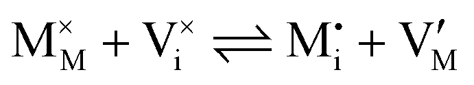
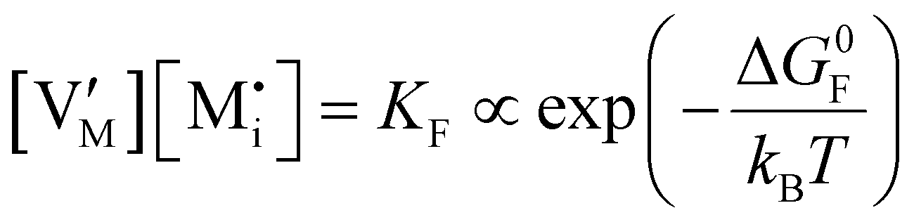
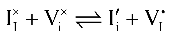
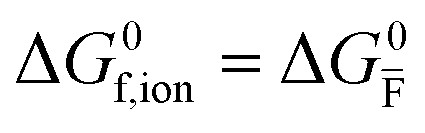
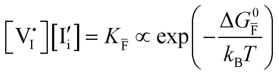
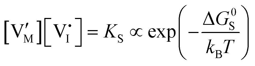
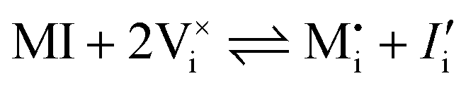
For systems that include mixed ionic–electronic conductors, as it is the case for hybrid perovskite devices, defect chemical thermodynamics can straightforwardly include the complexity of treating both electronic and ionic charge carriers, with simplified analytical treatments available for Brouwer (electroneutrality equation reduced to a proportionality relation) and Boltzmann (dilute defect concentrations) approximations.25 When discussing energy level diagrams, it then becomes convenient to extend the electronic representation to any number of additional ionic mobile defects giving significant contribution to the electrical conduction and electrostatic behavior of the device.26 To illustrate the complexity of the treatment even in simplified systems, we can consider the case of a binary, such as a metal halide MX, where five disorder reactions determine the equilibrium defect chemical situation. Specifically, considering the case of X = iodide, the treatment in Table 1 applies, also shown schematically in Fig. 1. This even ignores anti-site disorder that may become relevant at high temperatures.
 , KS and
  are the mass action constants (related to the intrinsic carrier concentrations) of the defect reactionsa
| Disorder type | Defect reaction (at equilibrium) | Standard reaction free energy ΔG0f | Mass-action law |
|---|---|---|---|
a Note that the four ionic disorder reactions are not independent, as 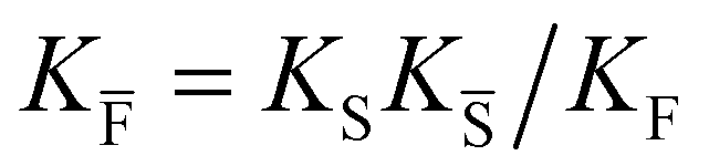 . .
|
|||
| Electronic | nil ⇌ e′ + h˙ | ΔG0f,eon = Eg |
|
| Ionic (Frenkel) |
|
ΔG0f,ion = ΔG0F |
|
| Ionic (anti-Frenkel) |
|
|
|
| Ionic (Schottky) |

|
ΔG0f,ion = ΔG0S |
|
| Ionic (anti-Schottky) |
|
|
|
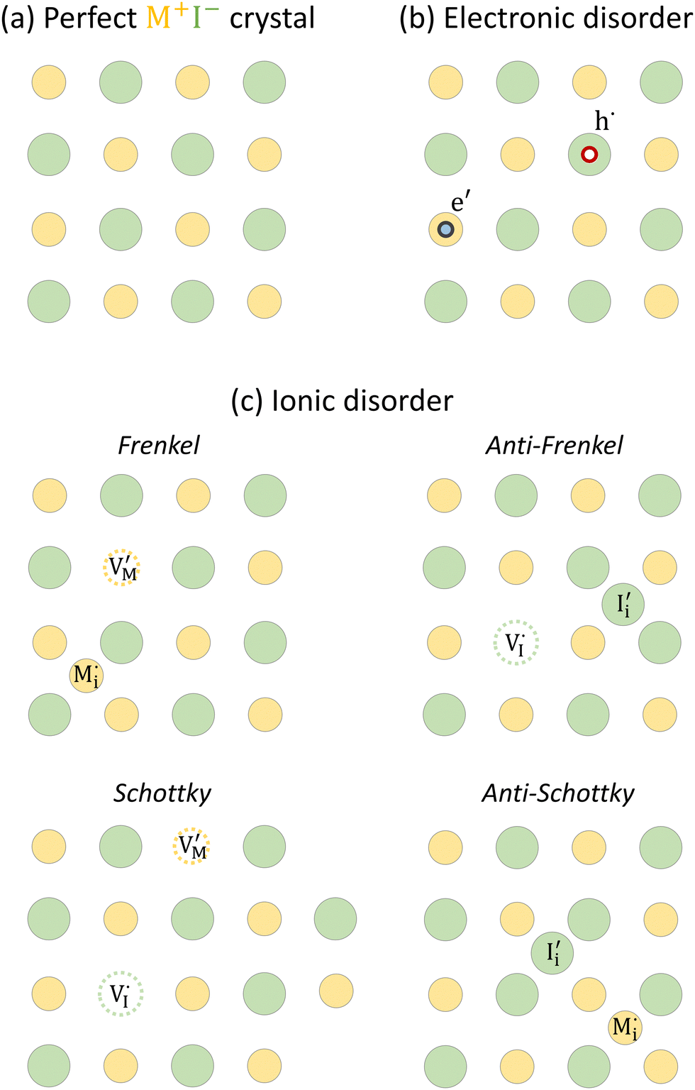 | ||
Fig. 1 (a) Perfect crystal of a square metal iodide lattice MI. (b) Electronic disorder involving electronic defects e′ and h˙. (c) Different types of ionic disorder involving metal and iodide point defects (interstitials  and and  and vacancies and vacancies  and and  ). ). | ||
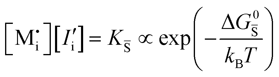
For the electronic disorder, the bandgap energy is the critical parameter determining the product of the electron and hole concentrations at equilibrium. A similar argument applies for each of the ionic disorder reactions, where an ionic “energy gap” indicates the standard free energy of defect formation, ΔG0f, and establishes the intrinsic equilibrium defect concentration based on the relevant defect mass action law.
Fig. 2 exemplifies such description, for the case of dominant anti-Frenkel disorder (small  ). Similarly to the electronic case, where conduction band electrons and valence band holes “populate” the electronic diagram, the relevant ionic charge carriers in the iodide diagram are (negative) iodide interstitials
  and (positive) iodide vacancies
  . Their concentrations can be defined based on the position of the electrochemical potential of iodide I− relative to the iodide interstitial and iodide vacancy standard potentials (0i and −0v). Furthermore, the chemical potential of iodine can be identified on the diagram based on
  . It is already clear from this figure, how the iodine chemical potential (or partial pressure, P(I2)) is connected to the stoichiometry of the material. When changing the P(I2) in the system, the position of both I− and e−, and therefore the concentration of all charge carriers, are varied.
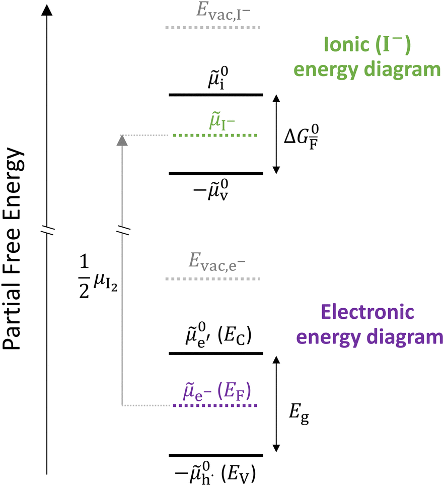 | ||
Fig. 2 Example of extended energy diagram of an iodide-based semiconductor including the electronic and the ionic (iodide) defect electrochemical potentials, standard electrochemical potentials (band edges) and vacuum levels. From these potentials it is possible to define the anti-Frenkel and the electronic disorder reaction standard free energies (electronic band gap, Eg, and ionic energy gap,  ) and the chemical potential of iodine, ) and the chemical potential of iodine,  . The potentials 0i and 0v refer to the standard electrochemical potentials of . The potentials 0i and 0v refer to the standard electrochemical potentials of  and and  respectively.4 respectively.4 | ||
In situations where ionic disorder reactions involving different constituents need to be accounted for, a simplified representation of the most relevant energy levels is still possible. Fig. 3 shows the complete electronic and ionic energy diagrams associated with all the disorder reactions in Table 1. Fig. 3(a) shows energy diagrams for both the positive and the negative ionic defects (note the different direction of the free energy axis following the charge sign). It is clear that, in principle, this description can be extended to any number of negative and positive ionic defects and allows one to schematically represent the chemical and electrochemical equilibrium of all the material's constituents. However, this approach can become particularly challenging for compounds for which more than two ionic constituents are involved, making it convenient to focus on the dominant ionic disorder. In Fig. 3(b), we propose a different visualization of the extended energy diagram. Here, the electronic and iodide energy levels are plotted referring to a partial free energy axis, G, similarly to (a), while the energy levels associated with the metal cation are shifted upwards by μMI, and refer to a separate axis, μMI − G. If the metal and iodide sublattices are in equilibrium, the position of the electrochemical potentials of I− and M+ on this effective diagram coincide. It is important to emphasize that in real systems, the latter condition may or may not be satisfied depending on the preparation conditions (more on this below).27 This representation allows one to visualize the standard reaction free enthalpies of all ionic disorders in Table 1 and to highlight the dominant (smallest) ionic energy gap (in this example ΔG0S). Based on this approach, even for compounds with more than two constituents, it is always possible to define the single ionic energy diagram (ionic disorder reaction) that dominates the properties of the mixed conductor.
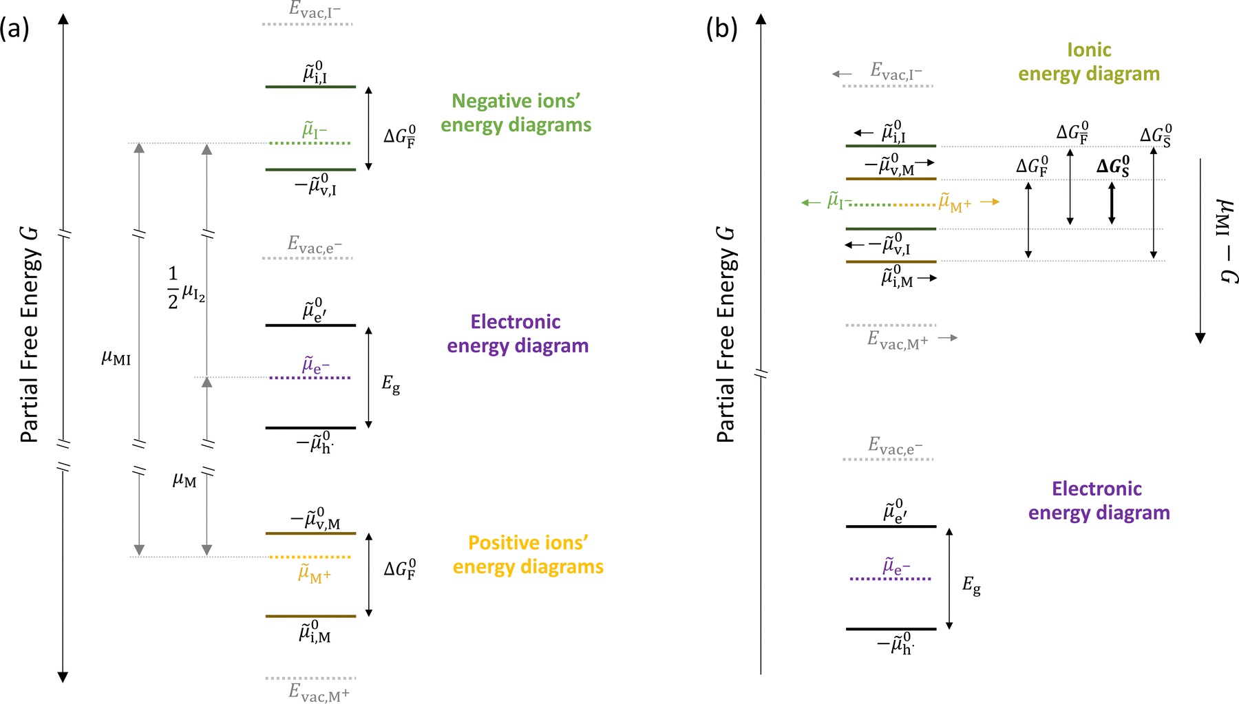 | ||
Fig. 3 (a) Extended energy diagram where the description of both negative and positive ionic constituents are included (in this example iodide and metal ions in the MI compound). In addition to the parameters introduced in Fig. 1, the Frenkel reaction standard free enthalpy is indicated as ΔG0F, while the standard potential for metal vacancy and interstitial follow the same nomenclature as described for iodide. The partial free energy axis is illustrated with different directions depending on the charge of the ion. The chemical potentials μM = M+ + e− and  are shown along with are shown along with  . The diagram in (b) is proposed as another visualization of (a), obtained by shifting the M+ energy diagram upwards by μMI. In this representation, the levels associated with the standard potentials of all defects highlight all the ionic energy gaps, including ΔG0S and . The diagram in (b) is proposed as another visualization of (a), obtained by shifting the M+ energy diagram upwards by μMI. In this representation, the levels associated with the standard potentials of all defects highlight all the ionic energy gaps, including ΔG0S and  (note that two energy axes are used for the energies of the different ions). By referring to (b), the dominant ionic disorder (in this case Schottky disorder) can be identified based on its lowest standard reaction free enthalpy. An effective ionic energy gap can therefore be defined based on the standard potentials associated with iodide and metal vacancies. (note that two energy axes are used for the energies of the different ions). By referring to (b), the dominant ionic disorder (in this case Schottky disorder) can be identified based on its lowest standard reaction free enthalpy. An effective ionic energy gap can therefore be defined based on the standard potentials associated with iodide and metal vacancies. | ||
B. Defect thermodynamics in MAPI
Hybrid halide perovskites consist of an ABX3 structure, with corner-sharing metal halide octahedra and a monovalent organic or inorganic cation.5,28–30 Owing to the multitude of elements, their defect chemistry is complex and requires considering multiple sublattices. As discussed in the previous section, concentrating on the dominant ionic disorder can be in most cases sufficient to interpret the material's behavior. For MAPI (see Fig. 4), Schottky disorder involving and
and  has previously been considered as one such possible dominant ionic disorder31–33 (note that negligible transport of Pb defects at room temperature is expected10). A diagram similar to the one shown in Fig. 3(b) (but where M is substituted with MA) is a good starting point to define the energetic picture of MAPI. Estimates for the values of the energy levels and energy gaps, which are fixed material properties, can be accessed experimentally or via simulations. To complete the energy diagram, the position of all electronic and ionic defects’ electrochemical potentials (and therefore their concentrations) needs to be defined. Such information can be obtained on the basis of the key disorder reactions (electronic and ionic), the reaction associated with the exchange of iodine with the gas phase and the condition of electroneutrality, as shown in Table 2.
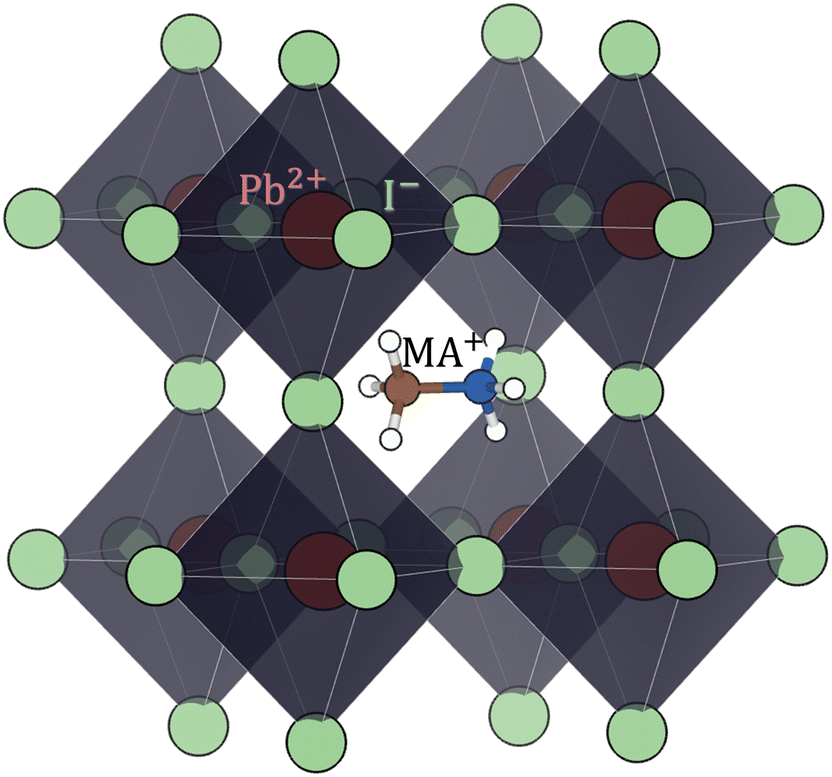 | ||
| Fig. 4 Perovskite (cubic) structure of methylammonium lead iodide (CH3NH3PbI3 or MAPI). Color code: Pb red, I light-green, C brown, N blue, H white. | ||
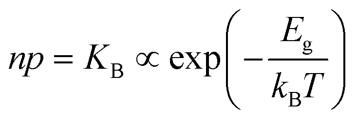
| Electronic disorder | nil ⇌ e′ + h˙ | [e′][h˙] = KB |
| Ionic (Schottky) disorder |

|
|
| Equilibrium with the gas phase |

|
|
| Electroneutrality |
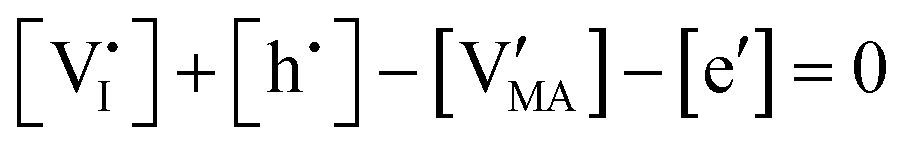
|
|
By assuming negligible transport of Pb defects, dominant Schottky disorder and no extrinsic doping, these equations yield the charge carrier concentrations in the system. In order to find a closed solution, the value for all the relevant thermodynamic state variables, which include the temperature and the partial pressures of all components, should be fixed. In the case where dopants (extrinsic or frozen-in defects) need to be considered in this evaluation, the set of equations can be modified accordingly.
The approximated solution to the system of equations resulting from these equilibria is represented in Fig. 5. Fig. 5(a) shows the iodine partial pressure dependence of the defects concentrations in a Kröger–Vink diagram for the simple intrinsic case described in Table 2. The relative trends for electronic and ionic defects are representative of most mixed-conductors, in that the standard reaction free energy associated with the dominant ionic disorder is lower than the bandgap ΔG0f < Eg (in this example, ΔG0f = ΔG0S). This implies that an intrinsic region (region I) with ionic defects being majority carriers is established. For the case where dopants or frozen-in defects are present, the disorder equations (for frozen-in defects e.g.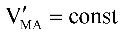 replacing Schottky equilibrium, or for a given dopant concentration e.g. [A′]) and the electroneutrality condition need to be modified accordingly (see Fig. 5(b) and (c), illustrating the expected defect concentration trends).31,34 We note that in Fig. 5(b), the “frozen” electrochemical potential associated with MA implies that other disorder reactions, which may have larger value of ΔG0f compared to ΔG0S (e.g. iodide anti-Frenkel disorder), may become relevant to the defects equilibrium, especially at high temperatures.35 For each of these cases, the equivalent picture from an energy level diagram point of view can be drawn, as shown at the bottom of Fig. 5. This representation can also be extended to include additional trapping effects, by considering the relevant reaction in the system of equations in Table 2.
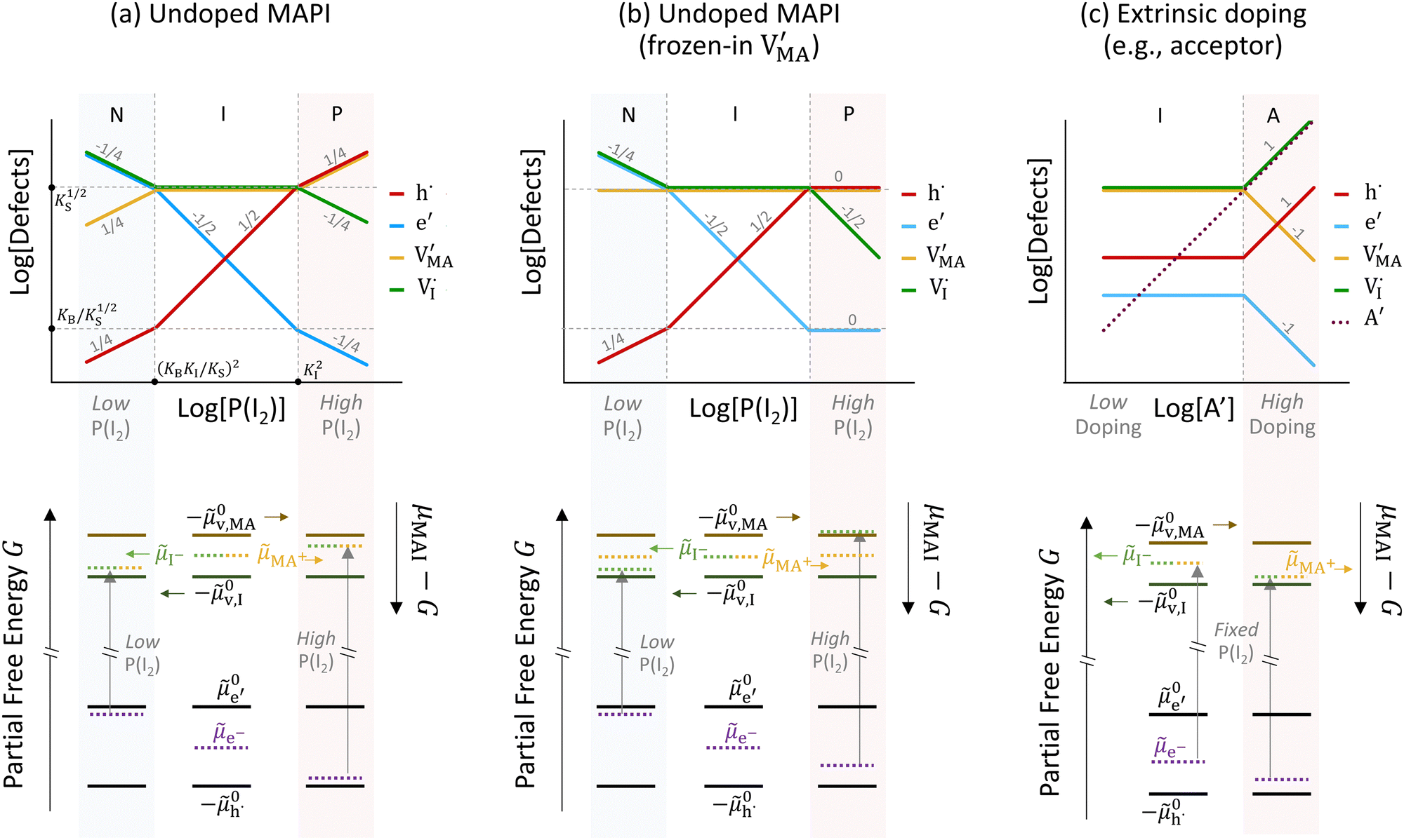 | ||
| Fig. 5 Defects concentrations in MAPI as function of different parameters: (a) iodine partial pressure dependence for the undoped case, (b) iodine partial pressure dependence, assuming frozen-in MA defects and (c) dopant (acceptor) concentration dependence. The numbers in the (top) Kröger–Vink diagrams indicate the approximate slope of the lines in each region. The corresponding generalized energy diagrams are included in each panel for different conditions, relating defect concentrations in the Kröger–Vink diagram to the position of the relevant electrochemical potentials . | ||
In summary, Kröger–Vink as well as generalized energy diagrams can provide a meaningful picture of the charge carrier equilibrium in relation to accessible thermodynamic variables (e.g. stoichiometry, varied through composition and P(I2)). So far, we discussed the case of bulk materials, where the assumption of electroneutrality is considered. In the next section, we extend the discussion to one-dimensional energy diagram representations of junctions in mixed conducting systems and focus on ionic effects leading to space charge equilibria.
C. Mixed conducting junctions and solar cells
The description of the equilibrium situation at junctions is a cornerstone of the device physics of solar cells and other electronic devices.36,37 Interfacial space charges influence properties of semiconductors and mixed conductors including conductivity, rectification, electronic recombination rate to name a few. The built-in potential (ϕbi) at a junction reflects, in the simplest case, the difference in chemical potential of the majority mobile charged species between the two materials. For example, in systems where only electronic charge carriers are mobile, the difference in work function, or difference in electronic chemical potential (Δμe−) between materials determines ϕbi. This is the case when, for example, a p-type and an n-type semiconductor are put into contact to form a p–n junction. The solution to the energy band alignment in the general case of heterojunctions between semiconductors is well established and relies, in the simple case, to similar arguments.38 We stress that the work-function of the materials determining Δμe− is not a fixed property. It is rather dependent on stoichiometry (see previous section) which can be fixed at the preparation stage, only in situations where ionic defects are immobile.The question of whether a stable p–n junction can be achieved between mixed ionic–electronic conductors is relevant for the fabrication of more complex device structures.39,40 For hybrid perovskite layers used in solar cells, depending on the details of the dominant recombination processes, the formation of such junction can benefit the photoconversion efficiency of the device.18Fig. 6(a) shows the case where two layers of MAPI with different work functions and different iodide chemical potential values are put into contact (only the relevant energy levels are plotted here). In these examples, for simplicity, we discuss the case of anti-Frenkel disorder only (the arguments that follow apply to Schottky disorder too) and we define the parameter ΔμI− as the difference in iodide chemical potential in the two materials, in analogy with the electronic picture. We describe the expected bending of all energy levels, which follow the changes in electrostatic potential as a function of time after the junction is formed (t > 0). At early time scales after contact (t = 0+), the energy level bending is determined by the fast equilibration of electronic species (e− becomes “flat”), while ionic equilibration has not occurred yet (I− is not “flat”). At this point, the situation is similar to a traditional n–p junction (left-to-right), where the  on the left side and the
  on the right behave like immobile donor and acceptor dopants respectively. At long time scales, when also ionic defects have equilibrated, if the difference in defect concentration between the two original materials concerns mobile defects (Fig. 6(a)), a homogeneous composition is obtained with no equilibrium space charge. Note that, as a result, also
  is constant across the junction. Therefore, varying stoichiometry to form a p–n junction in a material where all ionic defects have non-zero mobility is expected not to yield a stable and non-zero space charge potential in the device.41
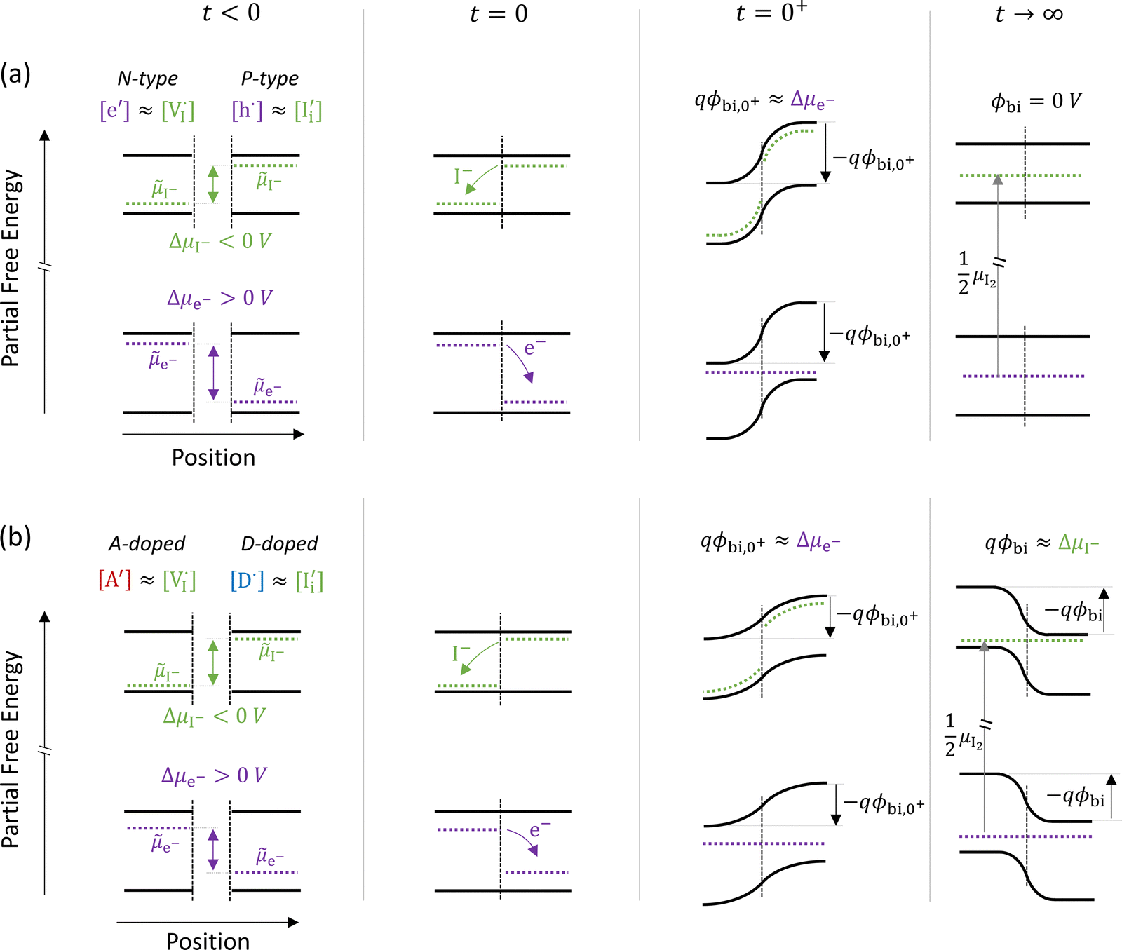 | ||
| Fig. 6 Ionic and electronic energy diagrams showing ionic effects at junctions of MAPI layers that are put into contact at time = 0 s (all diagrams follow the same notation as Fig. 3(a)). Equilibration upon contact between P-type and N-type layers for the case of (a) undoped materials and (b) materials doped with immobile acceptor (A′) and donor (D˙) species. For both cases, the local situation on a fast time scale (t = 0+) shows a built-in potential that reflects the electronic equilibration (qϕbi,0+ ≈ Δμe−). On a long time scale (t → ∞, after also ionic equilibration) the behavior differs in the two cases. In (a), where all relevant defects are assumed to be mobile, the difference in composition between the two layers vanishes and no built-in space charge potential is established between the two materials. In (b), a built-in potential is formed because of the extrinsic immobile defects in the two layers. Note that in the starting materials iodide defects are majority carriers (largely compensating the dopants), implying that the ionic charges determine the equilibrium situation for t → ∞ (qϕbi ≈ ΔμI−). | ||
The situation changes when the gradient in composition between the two layers involves defects that can be considered immobile (in the relevant temperature range). In Fig. 6(b) we show a schematic representation of an acceptor doped and a donor doped layer of the mixed conductor. Here, like in Fig. 6(a), Δμe− ≠ ΔμI−. In addition, ionic defects are majority carriers (largely compensating for the ionized dopants) in either layer, which is a representative situation of most mixed conductors, including hybrid perovskites, where ΔG0f < Eg, as discussed in the previous section. When the two layers are put into contact and electrochemical equilibrium of all mobile species is reached at long time scales, a non-zero space charge potential and, indeed, an electronic p–n (as well as an ionic vacancy–interstitial or v–i) junction is expected to form. Importantly, while immediately after the materials are put into contact (t = 0+) the space charge potential would once again reflect the electronic equilibration (qϕbi,0+ ≈ Δμe−), the equilibrium space charge potential at long time scales (t → ∞) is expected to correspond to ΔμI−. Even though from an electronic point of view the starting materials would tend to form an n–p junction (left to right) in this example, the long time scale situation would show a p–n junction instead. This is because the equilibrium distribution of electronic defects depends on the electrostatic potential profile, which is largely determined by the equilibration of the (majority carrier) ionic defects. This effect has previously also been referred to as the “fellow traveler effect”,42 and it stresses the importance of evaluating the equilibration of the majority carriers when building a picture of an interface between materials.
The examples in Fig. 6 emphasize that, for t → ∞, changes in defect concentrations at a mixed conducting junction extend throughout the bulk of the layers. It follows that the equilibrium situation at such junctions depends on the size of the system and on the boundary conditions far from the interface. Such long-range variations in properties become even more evident if we consider the case of two perovskite layers with different starting compositions (e.g. iodide and bromide based perovskites). Here, charge carrier equilibration between the two materials determines the final position of the relevant electrochemical potentials (e−, I− and Br−) based on the arguments discussed above for mobile and immobile defects. In addition, it influences the value of the equilibrium electronic (e.g. change in the absorption spectrum upon halide mixing between two films43) and ionic energy levels throughout the layers, based on the composition-dependence of such bulk properties. Importantly, this is in contrast with the behavior of interfaces between materials where only electronic charges equilibrate. In that case, changes in carrier concentrations due to variations in electric potential (qϕbi = Δμe−) are confined to the space charge region, and the behavior far from the junction is unvaried with respect to the situation before contact.
The equilibration at junctions described in Fig. 6 considers two layers of the same material (e.g. MAPI). When considering junctions between different materials, beside a nonzero difference in ionic and electronic chemical potentials (e.g. ΔμI− and Δμe−), differences in the standard potentials of electronic but also ionic defects can be expected.44 Due to the compositional variation across the interface, the formation of an equilibrium space charge can occur because of ionic equilibration, even in absence of immobile dopants. Equilibration at one such junction involving ion transfer (Fig. 7(a)) can result in the accumulation of ionic defects in proximity of the interface, with considerable effects on the interfacial partial conductivities (parallel or perpendicular to the interface).45,46
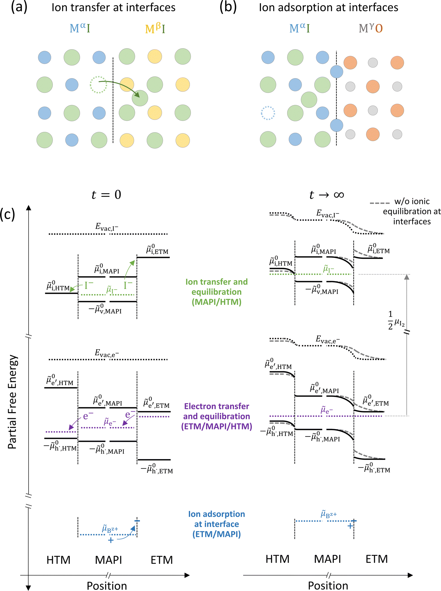 | ||
Fig. 7 (a) Ionic equilibration between two metal iodide phases MαI and MβI, where transfer of I− from MαI to MβI increases the concentration of  on the left side and of on the left side and of 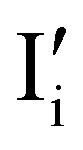 on the right side of the interface giving rise to an interfacial equilibrium space charge (ΔμI− ≠ 0 and different standard potentials of defect formations in the two phases are assumed). (b) Metal cation adsorption from a metal iodide MαI on the interface of a second phase (here an oxide MγO) induces a space charge region where positive defects are depleted and the concentration of negative defects (here on the right side of the interface giving rise to an interfacial equilibrium space charge (ΔμI− ≠ 0 and different standard potentials of defect formations in the two phases are assumed). (b) Metal cation adsorption from a metal iodide MαI on the interface of a second phase (here an oxide MγO) induces a space charge region where positive defects are depleted and the concentration of negative defects (here  and and  ) is increased. (c) Example of an extended ionic and electronic energy diagram of a MAPI solar cell in the dark at equilibrium where the interfaces are highlighted. Ion transfer (here I−) and ion adsorption (here Bz+ adsorbed at the MAPI/ETM interface, e.g. Pb2+ adsorbed on TiO2 surface47) can have significant repercussion on the chemical and electrostatic situation at interfaces. The situations upon contact (t = 0) and after equilibration (t → ∞) are shown. In the right diagram, dashed lines indicate the situation where ionic equilibration with contact materials is not considered. ) is increased. (c) Example of an extended ionic and electronic energy diagram of a MAPI solar cell in the dark at equilibrium where the interfaces are highlighted. Ion transfer (here I−) and ion adsorption (here Bz+ adsorbed at the MAPI/ETM interface, e.g. Pb2+ adsorbed on TiO2 surface47) can have significant repercussion on the chemical and electrostatic situation at interfaces. The situations upon contact (t = 0) and after equilibration (t → ∞) are shown. In the right diagram, dashed lines indicate the situation where ionic equilibration with contact materials is not considered. | ||
Besides ion transfer across an interface, ionic interactions limited to the preferential adsorption of mobile ionic defects on the surface of another material also results in the formation of a space charge region and redistribution of all other defects in the mixed conductors. For example, the adsorption of cations at the interface with a second phase produces an accumulation of negative defects and depletion of positive defects in the space charge layer (Fig. 7(b)).48 Let us now consider the implications of such effects for the case of a device stack where mixed-conducting materials are involved, such as a halide perovskite solar cell. In such device, the active layer (here MAPI) is sandwiched between a hole- and an electron- transporting material (HTM and ETM) all of which, in general, have different standard potentials for electronic and ionic defects (Fig. 7(c)).
For semiconducting materials with negligible ion transport, the equilibrium situation for the solar cell stack is predicted based on electronic aspects (Fermi level equilibration). Applying such strategy to the situation described in Fig. 7(c) envisages focusing on electron transfer (from the ETM to MAPI and from MAPI to HTM) equilibrating the electrochemical potential of electrons across the device. Starting from this picture, including the transport of mobile ionic charge carriers within the MAPI layer already has important consequences. Ionic equilibration establishes electroneutrality in the bulk of the mixed conductor with relatively narrow space charges forming at the interfaces with contacts.16,49–53 Assuming for example that mobile iodide vacancies are compensated by frozen-in defects in the bulk of MAPI, the relevant space charge situations would be a  accumulation layer (Gouy–Chapman) and a
  depletion layer (Mott–Schottky) on the MAPI side of the left and right interfaces, respectively. These space charges are compensated by the depletion of electronic majority carriers in the contact material side of either interface. The resulting electrostatic potential defines the energy level landscape, as highlighted with dashed gray lines (see right diagram in Fig. 7(c)).
Based on the ionic effects discussed above (Fig. 7(a) and (b)), further contributions due to ionic equilibration between MAPI and the contact materials can play an important role and deserve attention. For example, along with the perovskite's ionic energy diagram, the standard potential referring to iodide interstitials (0i) in the contact materials should be included. This level can lie at lower energies compared to 0i,MAPI (as shown in this example for 0i,HTM). While there may not be, ideally, any iodide in the electrode material before its contact with MAPI (ΔμI− is not defined at such interface), the space charge situation at the MAPI/contact interface can still be influenced by the equilibration of the iodine chemical potential between active layer and the transport layer. This can occur via iodide penetration from MAPI to the HTM, which can induce an increase in hole concentration as compensating charge. If significant compared to the background charge carrier concentration, this effect (p-type doping due to iodide) can affect the bulk work function of the HTM. The resulting change in Δμe− at the HTM/MAPI junction is then reflected in the equilibrium space charge potential dropping across the interface. Iodide interaction with and penetration in organic transport materials for hybrid perovskite based devices under bias were indeed observed in previous work.54–56 Iodine diffusion in various HTM organic semiconductors has been previously investigated, also highlighting the relation between electronic and ionic properties in these materials.57
Another contribution to the equilibration of mobile ionic or electronic defects can derive from their trapping and adsorption at interfaces. For the case of hybrid perovskites, this implies that an ionically-generated space charge potential can still be present despite ionic defects not being physically transferred across a junction and into the bulk of, for example, a contact material. Therefore, while some contact phases might have very large values of 0i, and equilibrium with respect to the ionic defects may not be reached in practical situations (in Fig. 7(c), I− is not shown in the ETM for t → ∞), the space charge situation can still be influenced by ionic interactions with the contact. In Fig. 7(c) the situation at the MAPI/ETM interface including interfacial adsorption of a positive ion is considered (equilibration of a generic Bz+ cation's electrochemical potential, Bz+, with the interface of the ETM, where “ionic surface states” are available at lower energy). This situation is expected for oxide materials such as TiO2, where evidence for a large space charge potential dropping on the MAPI side of the interface was ascribed to surface adsorption of Pb2+ ions.47 We note that only the simplified situation involving electrochemical equilibrium of non-reactive charge carriers has been described here. Redox reactions occurring at either contact layer on ionic adsorption and/or penetration should also be considered to build a more accurate picture.54,58,59
The discussion above emphasizes the importance of including the effect of mobile ionic defects in mixed conductors not only in the bulk but also at interfaces in the determination of the electrochemical equilibrium. We note that, even for devices under electrical and/or light bias, the ionic defect concentration predicted for hybrid perovskites are generally larger than most estimates of electronic charge densities for typical out of equilibrium conditions.33,60,61 The contribution deriving from the equilibration of mobile ionic defects at hybrid perovskite interfaces with contact materials is therefore likely to have significant implications also for solar cells under operation, an important question that deserves future investigation.
III. Conclusions
Research in the field of mixed ionic–electronic conducting materials, such as hybrid perovskites, hold great potential in the development of solar energy conversion and storage devices. A complete understanding of such systems requires models that accurately capture the behavior of and interaction between the several physical and chemical protagonists at play during device operation. Energy level diagrams are a useful tool to visualize the thermodynamic relations between electronic and ionic defects. We presented the use of such tools to express the connection between stoichiometry, defects concentration and charge carriers’ electrochemical potentials, both in the bulk and at interfaces. These representations stress that parameters such as electronic work functions and ionic concentrations are not fixed material properties. Instead, they depend on variables such as stoichiometry, doping and temperature, as a result of defect (electro)chemical equilibrium. In this context, generalized energy diagrams provide special emphasis on the relevant components’ chemical potentials (or partial pressures), which connect the “electronic and the ionic worlds”. The analysis of mixed conducting junctions indicates the importance of including ionic equilibration effects, such as ion transfer between phases and ion adsorption on a contact material's surface. Due to the large concentration of ionic defects in halide perovskites, and most mixed conducting systems, these effects can be dominant in the determination of the equilibrium space charge behavior at the device's interfaces. These concepts are particularly useful for bridging the gap between solid state ionics and semiconductor physics and thus relevant for the development of improved designs of mixed conducting devices that can optimize performance and stability.Conflicts of interest
There are no conflicts of interest to declare.Acknowledgements
We thank Dr. Max Hödl for providing feedback on this manuscript. DM is grateful to the Alexander von Humboldt foundation for financial support. Open Access funding provided by the Max Planck Society.References
- S. M. Sze and K. N. Kwok, Physics of Semiconductor Devices, John Wiley & Sons, Inc., Hoboken, New Jersey, 1995, vol. 10 Search PubMed.
- M. S. Whittingham, Chem. Rev., 2004, 104, 4271–4301 CrossRef CAS PubMed.
- S. M. Haile, Acta Mater., 2003, 51, 5981–6000 CrossRef CAS.
- J. Maier, Physical Chemistry of Ionic Materials, Wiley-VCH Verlag GmbH & Co. KGaA, 2005 Search PubMed.
- M. M. Lee, J. Teuscher, T. Miyasaka, T. N. Murakami and H. J. Snaith, Science, 2012, 338, 643–647 CrossRef CAS PubMed.
- G. Walch, B. Rotter, G. C. Brunauer, E. Esmaeili, A. K. Opitz, M. Kubicek, J. Summhammer, K. Ponweiser and J. Fleig, J. Mater. Chem. A, 2017, 5, 1637–1649 RSC.
- F. Podjaski, J. Kröger and B. V. Lotsch, Adv. Mater., 2018, 30, 1–9 CrossRef PubMed.
- T. Y. Yang, G. Gregori, N. Pellet, M. Grätzel and J. Maier, Angew. Chem., Int. Ed., 2015, 54, 7905–7910 CrossRef CAS PubMed.
- C. Eames, J. M. Frost, P. R. F. Barnes, B. C. O’Regan, A. Walsh and M. S. Islam, Nat. Commun., 2015, 6, 2–9 Search PubMed.
- A. Senocrate, I. Moudrakovski, G. Y. Kim, T.-Y. Yang, G. Gregori, M. Grätzel and J. Maier, Angew. Chem., Int. Ed., 2017, 56, 7755–7759 CrossRef CAS PubMed.
- S. Ravishankar, O. Almora, C. Echeverría-Arrondo, E. Ghahremanirad, C. Aranda, A. Guerrero, F. Fabregat-Santiago, A. Zaban, G. Garcia-Belmonte and J. Bisquert, J. Phys. Chem. Lett., 2017, 8, 915–921 CrossRef CAS PubMed.
- W. Tress, J. Phys. Chem. Lett., 2017, 8, 3106–3114 CrossRef CAS PubMed.
- D. Moia and J. Maier, ACS Energy Lett., 2021, 6, 1566–1576 CrossRef CAS.
- L. Bertoluzzi, R. A. Belisle, K. A. Bush, R. Cheacharoen, M. D. McGehee and B. C. O’Regan, J. Am. Chem. Soc., 2018, 140, 12775–12784 CrossRef CAS PubMed.
- A. Pockett, G. E. Eperon, N. Sakai, H. J. Snaith, L. M. Peter and P. J. Cameron, Phys. Chem. Chem. Phys., 2017, 19, 5959–5970 RSC.
- P. Calado, A. M. Telford, D. Bryant, X. Li, J. Nelson, B. C. O’Regan and P. R. F. Barnes, Nat. Commun., 2016, 7, 1–10 Search PubMed.
- N. E. Courtier, J. M. Cave, J. M. Foster, A. B. Walker and G. Richardson, Energy Environ. Sci., 2019, 12, 396–409 RSC.
- T. Kirchartz, J. Bisquert, I. Mora-Sero and G. Garcia-Belmonte, Phys. Chem. Chem. Phys., 2015, 17, 4007–4014 RSC.
- M. Stolterfoht, P. Caprioglio, C. M. Wolff, J. A. Márquez, J. Nordmann, S. Zhang, D. Rothhardt, U. Hörmann, Y. Amir, A. Redinger, L. Kegelmann, F. Zu, S. Albrecht, N. Koch, T. Kirchartz, M. Saliba, T. Unold and D. Neher, Energy Environ. Sci., 2019, 12, 2778–2788 RSC.
- T. Hellmann, C. Das, T. Abzieher, J. A. Schwenzer, M. Wussler, R. Dachauer, U. W. Paetzold, W. Jaegermann and T. Mayer, Adv. Energy Mater., 2020, 10, 1–11 Search PubMed.
- S. T. Birkhold, J. T. Precht, R. Giridharagopal, G. E. Eperon, L. Schmidt-mende and D. S. Ginger, J. Phys. Chem. C, 2018, 122, 12633–12639 CrossRef CAS.
- J. Jamnik, J. Maier and S. Pejovnik, Solid State Ionics, 1995, 75, 51–58 CrossRef CAS.
- J. Maier, Angew. Chem., Int. Ed. Engl., 1993, 32, 313–335 CrossRef.
- A. Kahn, Mater. Horiz., 2016, 3, 7–10 RSC.
- G. Brouwer, Philips Res. Rep., 1954, 9, 366–376 CAS.
- J. Maier, Solid State Ionics, 2001, 143, 17–23 CrossRef CAS.
- J. Maier, Phys. Chem. Chem. Phys., 2003, 5, 2164–2173 RSC.
- D. Weber, Z. Naturforsch., B: Anorg. Chem., Org. Chem., 1978, 33, 1443–1445 CrossRef.
- A. Kojima, K. Teshima, Y. Shirai and T. Miyasaka, J. Am. Chem. Soc., 2009, 131, 6050–6051 CrossRef CAS PubMed.
- H. S. Kim, C. R. Lee, J. H. Im, K. B. Lee, T. Moehl, A. Marchioro, S. J. Moon, R. Humphry-Baker, J. H. Yum, J. E. Moser, M. Grätzel and N. G. Park, Sci. Rep., 2012, 2, 1–7 Search PubMed.
- A. Senocrate, T. Y. Yang, G. Gregori, G. Y. Kim, M. Grätzel and J. Maier, Solid State Ionics, 2018, 321, 69–74 CrossRef CAS.
- J. Mizusaki, K. Arai and K. Fueki, Solid State Ionics, 1983, 11, 203–211 CrossRef CAS.
- A. Walsh, D. O. Scanlon, S. Chen, X. G. Gong and S. H. Wei, Angew. Chem., Int. Ed., 2015, 54, 1791–1794 CrossRef CAS PubMed.
- A. Senocrate and J. Maier, J. Am. Chem. Soc., 2019, 141, 8382–8396 CrossRef CAS PubMed.
- D. Barboni and R. A. De Souza, Energy Environ. Sci., 2018, 11, 3266–3274 RSC.
- P. Schulz, ACS Energy Lett., 2018, 3, 1287–1293 CrossRef CAS.
- P. Schulz, D. Cahen and A. Kahn, Chem. Rev., 2019, 119, 3349–3417 CrossRef CAS PubMed.
- A. Klein, Thin Solid Films, 2012, 520, 3721–3728 CrossRef CAS.
- I. Riess, Phys. Rev. B: Condens. Matter Mater. Phys., 1987, 35, 5740–5743 CrossRef CAS PubMed.
- J. F. Guillemoles, I. Lubomirsky, I. Riess and D. Cahen, J. Phys. Chem., 1995, 99, 14486–14493 CrossRef.
- P. Calado and P. R. F. Barnes, Nat. Energy, 2021, 6, 589–591 CrossRef CAS.
- J. Maier, Phys. Chem. Chem. Phys., 1989, 93, 1474–1479 CAS.
- J. Cho, J. T. Dubose, A. N. T. Le and P. V. Kamat, ACS Mater. Lett., 2020, 2, 565–570 CrossRef CAS.
- R. Merkle and J. Maier, Z. Phys. Chem., 2022, 236, 991–999 CrossRef CAS.
- N. Sata, K. Eberman, K. Eberl and J. Maier, Nature, 2000, 408, 946–949 CrossRef CAS PubMed.
- J. Maier, Nat. Mater., 2005, 4, 805–815 CrossRef CAS PubMed.
- G. Y. Kim, A. Senocrate, D. Moia and J. Maier, Adv. Funct. Mater., 2020, 30, 1–9 Search PubMed.
- J. Maier, Prog. Solid State Chem., 1995, 23, 171–263 CrossRef CAS.
- R. A. Belisle, W. H. Nguyen, A. R. Bowring, P. Calado, X. Li, S. J. C. Irvine, M. D. McGehee, P. R. F. Barnes and B. C. O’Regan, Energy Environ. Sci., 2017, 10, 192–204 RSC.
- S. Van Reenen, M. Kemerink and H. J. Snaith, J. Phys. Chem. Lett., 2015, 6, 3808–3814 CrossRef CAS PubMed.
- L. Bertoluzzi, C. C. Boyd, N. Rolston, J. Xu, R. Prasanna, B. C. O’Regan and M. D. McGehee, Joule, 2020, 4, 109–127 CrossRef CAS.
- D. A. Jacobs, Y. Wu, H. Shen, C. Barugkin, F. J. Beck, T. P. White, K. Weber and K. R. Catchpole, Phys. Chem. Chem. Phys., 2017, 19, 3094–3103 RSC.
- G. Richardson, S. E. J. O’Kane, R. G. Niemann, T. A. Peltola, J. M. Foster, P. J. Cameron and A. B. Walker, Energy Environ. Sci., 2016, 9, 1476–1485 RSC.
- J. Carrillo, A. Guerrero, S. Rahimnejad, O. Almora, I. Zarazua, E. Mas-Marza, J. Bisquert and G. Garcia-Belmonte, Adv. Energy Mater., 2016, 6, 1–7 Search PubMed.
- R. A. Z. Razera, D. A. Jacobs, F. Fu, P. Fiala, M. Dussouillez, F. Sahli, T. C. J. Yang, L. Ding, A. Walter, A. F. Feil, H. I. Boudinov, S. Nicolay, C. Ballif and Q. Jeangros, J. Mater. Chem. A, 2020, 8, 242–250 RSC.
- R. A. Kerner, L. Zhao, S. P. Harvey, J. J. Berry, J. Schwartz and B. P. Rand, ACS Energy Lett., 2020, 5, 3352–3356 CrossRef CAS.
- R. A. Kerner, S. Heo, K. Roh, K. MacMillan, B. W. Larson and B. P. Rand, ACS Energy Lett., 2021, 6, 501–508 CrossRef CAS.
- R. A. Kerner and B. P. Rand, J. Phys. Chem. Lett., 2017, 8, 2298–2303 CrossRef CAS PubMed.
- L. Zhao, R. A. Kerner, Z. Xiao, Y. L. Lin, K. M. Lee, J. Schwartz and B. P. Rand, ACS Energy Lett., 2016, 1, 595–602 CrossRef CAS.
- B. C. O’Regan, P. R. F. Barnes, X. Li, C. Law, E. Palomares and J. M. Marin-beloqui, J. Am. Chem. Soc., 2015, 137, 5087–5099 CrossRef PubMed.
- S. Wheeler, D. Bryant, J. Troughton, T. Kirchartz, T. Watson, J. Nelson and J. R. Durrant, J. Phys. Chem. C, 2017, 121, 13496–13506 CrossRef CAS.
| This journal is © The Royal Society of Chemistry 2023 |