
 Open Access Article
 This Open Access Article is licensed under a
 Creative Commons Attribution 3.0 Unported Licence
Interface-related phenomena in epitaxial complex oxide ferroics across different thin film platforms: opportunities and challenges
Judith L.
MacManus-Driscoll
*a,
Rui
Wu
 *ab and
Weiwei
Li
*ac
*ab and
Weiwei
Li
*ac
aDepartment of Materials Science and Metallurgy, University of Cambridge, Cambridge, CB3 0FS, UK. E-mail: jld35@cam.ac.uk; ruiwu001@scut.edu.cn; wl337@nuaa.edu.cn
bSpin-X Institute, School of Physics and Optoelectronics, State Key Laboratory of Luminescent Materials and Devices, Guangdong-Hong Kong-Macao Joint Laboratory of Optoelectronic and Magnetic Functional Materials, South China University of Technology, Guangzhou 511442, China
cMIIT Key Laboratory of Aerospace Information Materials and Physics, State Key Laboratory of Mechanics and Control of Mechanical Structures, College of Physics, Nanjing University of Aeronautics and Astronautics, Nanjing 211106, China
First published on 21st February 2023
Abstract
Interfaces in complex oxides give rise to fascinating new physical phenomena arising from the interconnected spin, lattice, charge and orbital degrees of freedom. Most commonly, interfaces are engineered in epitaxial superlattice films. Of growing interest also are epitaxial vertically aligned nanocomposite films where interfaces form by self-assembly. These two thin film forms offer different capabilities for materials tuning and have been explored largely separately from one another. Ferroics (ferroelectric, ferromagnetic, multiferroic) are among the most fascinating phenomena to be manipulated using interface effects. Hence, in this review we compare and contrast the ferroic properties that arise in these two different film forms, highlighting exemplary materials combinations which demonstrate novel, enhanced and/or emergent ferroic functionalities. We discuss the origins of the observed functionalities and propose where knowledge can be translated from one materials form to another, to potentially produce new functionalities. Finally, for the two different film forms we present a perspective on underexplored/emerging research directions.
 Judith L. MacManus-Driscoll | Prof. Judith MacManus-Driscoll is a Professor in the Materials Science & Metallurgy at the University of Cambridge. She is also Royal Academy of Engineering Chair in Emerging Technologies. Her research work is in the area of oxide thin film engineering for low power electronic and energy devices. She is interested both in understanding basic functionalities and in engineering new interfacial-driven properties. |
 Rui Wu | Prof. Rui Wu is a Professor in Spin-X Institute at South China University of Technology (SCUT). His research interests focus on functional oxide thin films and 2-dimensional materials for spintronic devices applications. He received his PhD degree from Peking University (2015). He did training as a postdoctoral researcher from 2015 to 2020 at the University of Cambridge and the Norwegian University of Science and Technology (NTNU). |
 Weiwei Li | Prof. Weiwei Li is a Professor in the College of Physics at the Nanjing University of Aeronautics and Astronautics. His research interests focus on the complex functional oxide thin films for low-energy consumption (opto-)electronic devices and energy conversion/storage. He obtained his PhD degree from Soochow University in 2015, followed by working as a research associate in the Department of Materials Science & Metallurgy at the University of Cambridge from 2015 to 2021. |
1. Introduction
Strongly correlated oxides are fascinating and widely explored functional materials, with an unrivalled range of physical properties. Their most perfect and applicable form is as epitaxial films. To exploit emergent and strain-related interface effects in epitaxial films, typically either superlattice (SL) or vertically aligned nanocomposite (VAN) film forms are studied, each offering different phenomena.While there have been many important reviews on emergent functional properties of SL1 and VAN,2 a broader article comparing the phenomena in these different structures has not been presented. The two fields have typically followed quite separate paths by quite separate groups. At first glance, this seems somewhat surprising since the tools for creating the films, the functional materials being studied, and the desired multifunctionalities being aimed for are either the same or are similar. On the other hand, there are subtle differences in approach and knowledge-sets for creating each film form which has precluded overlap between them.
In this review we focus on ferroic properties in the two materials as these are particularly exciting and because they exemplify the salient effects offered by each platform. We aim to present the key differences in the functionalities achieved by exploiting interface effects in the two thin film forms, comparing the merits and drawbacks of each and the reasons for those differences. We also aim to give insight into what can be learned from one form for the benefit of the other. We highlight novel phenomena and promising areas for future studies. We first compare the basic growth and structural features of each form and then we compare their exemplar ferroic properties. After that, we then explore in more detail the individual ferroelectric, ferromagnetic and multiferroic properties of SLs and follow this by exploring the same three phenomena for VANs. After each SL ferroics section, we discuss what can be learned for VAN from the SL field. Where appropriate, we do this also for each VAN section also. Finally, we propose future perspectives for each, including underexplored/emerging research directions.
Ferroics are fascinating exemplar materials to explore for our different film forms as they exhibit very wide ranging and tunable properties with huge future applications prospects. Ferroics refer to materials presenting at least one intrinsic long-range ordering such as magnetization, electric polarization, etc. The first application of a ferroic was in lodestone, which was used as a simple magnet and later as a compass, more than 2000 years ago. An understanding of the basic origin of the ferroics was not achieved until the beginning of the last century with the help of quantum mechanics. Over the past century, and in particular in the last decades, many new materials, of metallic, semiconducting, insulating and even organic materials classes, have been added to the ferroics collection. This endows them with very important applications in a range of current electronics devices.
Ferroelectrics have a spontaneous electric polarization that can be switched by an external electric field,3 or by mechanical or optical stimuli.4 They are used in a wide range of radio-frequency and microwave devices, as well in thermal sensors, actuators, and transducers, etc.,5 and there is also strong interest for non-volatile memory.6 Magnetic thin films are used in magnetic recording media, the leading technology for mass data storage.7 Also, magnetic random-access memory (MRAM) could be the winning technology for next-generation ‘universal’ memory.8 Another important ferroic form is multiferroics where two ferroic properties coexist, giving promise of magnetoelectricity for multi-state memory in which there is control of magnetism with an electric field. Magnetoelectric random access memory (MeRAM) possesses all advantages of MRAM, but crucially at much lower energy consumption.9
For the field of ferroic electronics, thin films of transition metal oxides (TMOs) are of particular interest as they show a very wide range of ferroic properties which are linked to the d orbitals in TM ions. These orbitals, in the presence of a strong ligand field from oxygen ions bonded to the TM ions, produce a wide range of excited states, polarisation effects, and electronic properties. These effects are highly tunable owing to the strong correlation between charge, orbital and structural degrees of freedom of the TM–O bond. Of the TMOs, oxide perovskites have been most widely studied owing to their wide ranging functionalities, ease of growth by pulsed laser deposition (PLD) and compatibility with widely available perovskite single crystals.
If one adds an interface between different TMOs, then symmetry breaking effects, strain and strain-relieving defects6 at the interface add yet another handle of tunability, coupling and complexity to TMO functionality. Interfaces and the consequent coupling between two different TMOs can be accomplished effectively in either SL or VAN forms. Conventional SLs have interfaces parallel to the substrate and are grown one layer at a time using vacuum deposition methods. There are a couple of notable exceptions where SLs form by self-assembly from a combined target material, i.e. TiO2/VO210 and YBa2Cu3O7−x/BaZrO311 the first formed by spinodal decomposition and the second by phase separation.
The schematics of SL and VAN epitaxial thin film forms, grown mainly by PLD, but less often also by molecular beam epitaxy (MBE) for SL films, are shown schematically in Fig. 1, with structural characteristics and interface-related phenomena shown. For far-from-equilibrium processing methods (including PLD but also sputtering), while vertical columnar grains form in standard planar films, these are different to the VAN columnar grains. For VAN columnar grains, their growth is controlled by vertical epitaxy with the matrix phase in the film and there is vertical epitaxial strain associated with this, as well as potential for interface phenomena at these interfaces, whereas for standard planar films such effects do not occur. The remaining figures in the paper go into more depth than Fig. 1, explaining in detail the origins of the interface phenomena in both VAN and SL films.
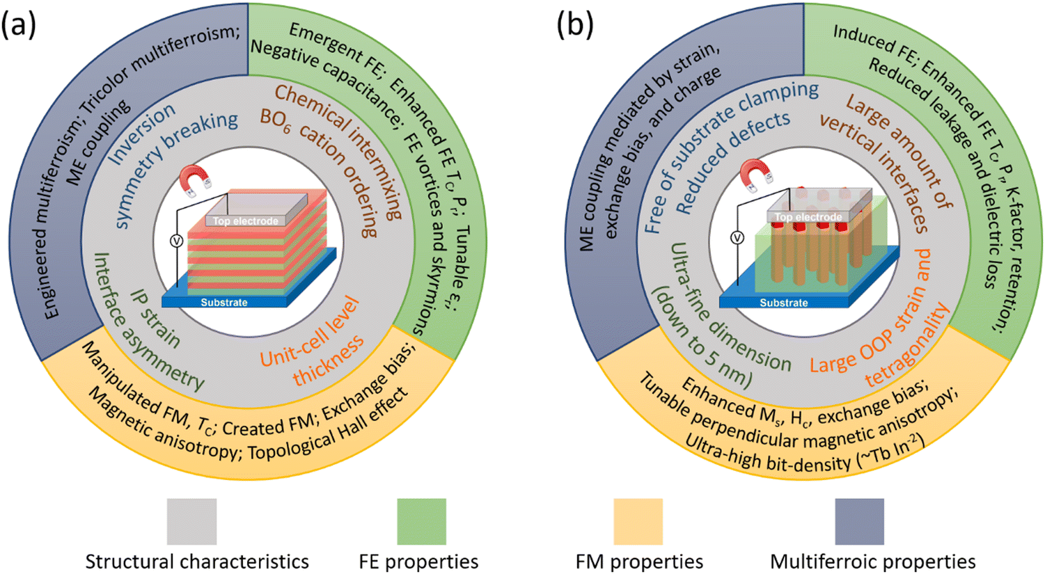 | ||
| Fig. 1 Schematic diagrams showing structural characteristics (inner ring) and observed interface-related phenomena (outer ring) in epitaxial ferroic thin films formed from (a) SL structures and (b) VAN structures. Tricolor multiferroism is a kind of multiferroism induced in a three-component SL. See Fig. 2–8 for more details about how both structural and physical effects link to the observed interface-related phenomena. | ||
We note that multilayer (ML) films are similar to SL films, except they contain fewer layers (<∼5) than SL (>∼5), and the individual film layers are typically thicker than for SL (e.g. >15–30 unit cells for ML, and <15 unit cells for SL). In this paper, MLs are discussed where SLs have not yet been presented.
Both SLs and VANs have large area interfaces which enable physical phenomena to be both precisely tuned, e.g. using external stimuli such as magnetic or electric fields, and probed, e.g. using spectroscopic tools. Table 1 compares the growth and structural features of the two different materials forms.
| SL | VAN | |
|---|---|---|
| a The substrate influences strain only for ≤20 nm film thickness. Above this thickness, the vertical strain dominates.12 Hence, strain can be 3-dimensional with auxetic-like effects possible.13 b >1000 nm thicknesses possible. c Insufficient time in SL to nucleate and grow dislocations between layers so other defects form to alleviate strain. d Growth of vertical interfaces slow, enabling misfit dislocations to form.14 e Interfaces become less 2D-like as the number of superlattice layers increases above ∼10–20 layers and then the layers roughen. f Interface directions can deviate from the vertical direction, and hence can be tortuous. g In VAN, there can be chemical segregation of species at an atomic level right at the interface.15 This is not the same as chemical intermixing which occurs by reaction between two materials at either side of the interface. This is the case for SL where you have two separate materials grown from separate targets and which can then react at the interface during growth. In VAN, if intermixing is thermodynamically favoured it will have already occurred when the materials are all mixed together in the ceramic target. It means there is not additional chemical reaction/chemical intermixing at the interfaces between the two materials. | ||
| Complexity of growth process? | Higher | Lower |
| Very wide variety of materials combinations possible? | Y | N |
| Intermixing at interfaces? | Few unit cell level | Unit cell levelg |
| Substrate control of strain | Y | Na |
| Easy and uniform control of in-plane strain | Y (in films <20 nm) | N |
| Easy and uniform control of out-of-plane strain | N | Y (in films >20 nm)b |
| Misfit dislocations at interfaces | Nc | Yd |
| Dimensionality of interfaces | 2D | Non-ideal 2D |
| Deviation from dimensionality | Very lowe | Widef |
The overall drive in research on VANs has been more applied owing to simplicity of growth, and the ability to grow relatively thick, highly strained films resulting from a high density of vertical interfaces, whereas for SL films the focus has been on basic science, enabled by the growth of well-defined 2D interfaces. The growth of SLs is more complex than VAN, requiring reflection high energy electron diffraction (RHEED) and precise substrate heating to carefully control the thickness and qualities of the individual layers. On the other hand, SL growth produces much more well-defined 2D interfaces than VAN, making them ideally suited to exploring emergent interface effects.
VANs grow in a one-shot process from a single ceramic target, and the VAN structure forms epitaxially by self-assembly in the film. The growth of VANs does not need RHEED or very precise control of growth conditions as for epitaxial SLs where each film layer must be very smooth. However, to create new interface-coupled effects in well-aligned VANs, one needs to predict which phases will self-assemble in a given VAN film, starting from the target of all the mixed cations. This requires a greater knowledge of the stabilising forces of epitaxy with the substrate and thermodynamics of the possible phases that can arise from the global cation mix. A simple example is as follows: you may want to grow a VAN of NiO and Fe3O4 on a standard single crystal substrate. Depending on the Ni![[thin space (1/6-em)]](https://www.rsc.org/images/entities/char_2009.gif) :Fe ratio in the target, and assuming standard growth conditions, you will achieve either NiO + NiFe2O4 or NiFe2O4 + Fe3O4, and hence not the desired NiO and Fe3O4 mix. This example does not mean you will always achieve a ternary phase and a binary phase when the aim is for two binaries. VANs of binaries are indeed possible where intermediate ternaries do not form, e.g. TiO2 + VO2.16
:Fe ratio in the target, and assuming standard growth conditions, you will achieve either NiO + NiFe2O4 or NiFe2O4 + Fe3O4, and hence not the desired NiO and Fe3O4 mix. This example does not mean you will always achieve a ternary phase and a binary phase when the aim is for two binaries. VANs of binaries are indeed possible where intermediate ternaries do not form, e.g. TiO2 + VO2.16
The basic ground rules for growing VANs have been set out in comprehensive reviews, the first in 201017 with others building on the understanding subsequently.18 Suffice for this article is to note that in VAN films a matrix phase forms in the film with an inclusion phases. The inclusion phase should be structurally dissimilar to the matrix phase to prevent ready mixing of the two materials during growth. This is a different situation to SLs where structurally similar phases are required so that the artificial interfaces that form between them are more perfect. If there is a sufficiently high-volume fraction of the inclusion, it typically forms as nanopillars which grow embedded in the matrix phase. The nanopillars are fine, typically <20 nm in diameter and ∼5–50 nm pitch, controllable by selecting the appropriate growth parameters.2b
In VAN films the vertical interfaces formed with the matrix can be faceted semi-coherent interfaces or cylindrical surface incoherent interfaces. We term both types of interfaces non-ideal 2D. Owing to the fine pillar dimensions and pitch, it is possible for large vertical and uniform strains to be induced in the matrix from the pillar scaffolds.17,19,20 More details about the large vertical strains for VAN films are discussed in Section 6. The most perfect VANs are achieved when the matrix material is structurally the same or very similar to the substrate.15b Here, a single interface type (lowest lattice mismatch one) will form, enabling the high density, highly vertical interfaces to be created. For this situation, strain control to >1 micron film thickness has been shown.14,21 On the other hand, when the matrix material is lattice mismatched to the substrate and also to the second phase in the VAN film, the films grow less perfectly.22 Here, the interfaces have higher energy than when films are isostructural. To minimise the vertical interface energies, a range of different interfaces with similar interfacial energy can form, which leads to meandering of the vertical interfaces. Examples are shown in later figures in this paper. More work needs to be done to give a more quantitative description of VAN microstructures in relation to the properties of the two materials in the film and the growth conditions, and the consequences of the nature of the meandered microstructure on the strain levels in the films and thus the functional properties.
The kinetics of interface formation are very different for SL and VAN films which influences the perfection of the interfaces (and regions in the vicinity of the interfaces). For VAN films the vertical interfaces grow slowly, allowing misfit dislocations to form to partially relieve the strain, whereas for SLs ‘forced’ artificial interfaces form very rapidly, which can lead to the formation of point-like defects to relieve any interfacial strain effects.14 Also, since the VAN interfaces are formed at equilibrium and are self-assembled, they are not chemically intermixed as SL film interfaces often are.1a This, however, comes at the expense of a lower possible number of materials permutations that can be combined together.
The most enhanced or novel ferroic properties from SL and VAN films, i.e. the maximum possible values or novel ferroic properties achieved for each materials form, are summarised in Table 2. Different materials pairs between SL and VAN are compared because different pairs are compatible for each thin film form. Hence for VAN, one typically requires structurally dissimilar materials to prevent a single mixed phase from forming, while for SL structurally similar materials are required to enable high quality interfaces to form. From Table 2, it is clear that the two materials forms offer quite different maximum or novel effects. An important question is what can be learned from one materials platform and translated to another? For example, could a topological Hall effect be achieved in VAN similar to SL, or could a self-biased magnetoelectric effect be achieved in SL similar to VAN?
| SL | VAN | |
|---|---|---|
| FM – ferromagnetism. FE – ferroelectricity, ME – magnetoelectricity. DME = direct magnetoelectric coefficient, CME = converse magnetoelectric coefficient. | ||
| FE | In 10–200 nm thick films | In ∼micron thick films |
| T C of BaTiO3/SrTiO3 increased by several hundred K23 | T C of BaTiO3–Sm2O3 VAN increased by several hundred K21 | |
| P r ∼ 16.5 μC cm−2, the value is doubled in SrTiO3/BaTiO3/CaTiO3cf. plain BaTiO3 film24 | P r ∼ 12.1 μC cm−2, the value is trebled in (Ba,Sr)TiO3–Sm2O3 VAN film ∼ cf. plain (Ba,Sr)TiO3 film25 | |
| Tunability values ∼40% at 200 kV cm−1 and 300 K in SrTiO3/BaTiO3/SrO26 which is >3 higher than for BaTiO3 plain films | Tunability values are ∼75% at 200 kV cm−1 and 300 K in (Ba,Sr)TiO3–Sm2O3 VAN film which is ∼40% higher than for (Ba,Sr)TiO3 plain film.27 Also, loss scales with tunability, which is opposite to plain films. | |
| Negative capacitance observed in Ba0.8Sr0.2TiO3/LaAlO3 and PbTiO3/SrTiO3 at 300 K28 | Negative capacitance not yet observed | |
| Polar vortices observed in PbTiO3/SrTiO328b,29 | Polar vortices not yet observed | |
| FM | In-plane exchange bias as high as 3 kOe induced in CaRuO3/CaMnO3 at 10 K30 | Perpendicular exchange bias of ∼0.91 kOe at room temperature obtained in NiO–NiFe2O4 VAN22cf. ∼0.1 kOe in NiO–NiFe2O4 bilayer at room temperature.31 |
| High interfacial magnetization of up to 2.5μB (396 emu cm−3) achieved in LaFeO3/LaCrO332 | Saturation magnetisation in Fe3O4–BiFeO3 VAN film ∼900 emu cm−3cf. ∼300 emu cm−3 in pure Fe3O4 film with similiar thickness33 | |
| High TC ferromagnetism of up to 375 K created at interfaces from non-magnetic parent materials in LaFeO3/LaCrO332 | Ferro/ferrimagnets with several-hundred-K TC created from AFM parent material ZnFe2O434 | |
| Perpendicular magnetic anisotropy (Keff) of 4 × 10⁶ erg cm−3 (∼13 kOe) realized in La1−xSrxMnO3/SrIrO3 at 10 K35 | Perpendicular magnetic anisotropy of 85 kOe induced in BaTiO3–CoFe2O4 at 300 K via strain36 | |
| Topological Hall effect up to 75 μΩ cm observed in LaMnO3/SrIrO3 at 10 K37 | No topological Hall effect observed | |
| DME coefficient αME up to 55 V cm−1 Oe−1 at 300 K observed in BaTiO3/BiFeO338 | DME coefficient αME up to 20 V cm−1 Oe−1 at 300 K measured in BiFeO3–CoFe2O439 | |
| ME | No sizable CME yet observed | Self-biased CME effect at room temperature with ME coefficient of ∼1.4 × 10⁻⁹ s m−1 at 300 K achieved in Na0.5Bi0.5TiO3–NiO–NiFe2O440 |
The rest of the paper expands on the information in Table 2, discussing the different ferroic phenomena of ferroelectricity, ferromagnetism and multiferroicity observed in SL films (part A) and VAN films (part B), with potential synergies between the two film forms noted. Finally, an overall summary, perspective and conclusions are presented (part C).
A. Ferroics in superlattice films
2. Ferroelectric phenomena in superlattice films
Ferroelectric polarization in oxide perovskites of the ABO3 formula is induced by polar displacement in B-site cations at the centres of BO6 octahedral cages, or displacement of A-site (lone-pair active) cations which sit between the octahedra. In SL films, a wide range of fascinating ferroelectric properties have been observed, e.g. ferroelectricity induced at the interfaces between two non-ferroelectric systems, enhanced TCs and higher remanent polarization values, improved dielectric tunability, negative capacitance effects, and polar skyrmions/vortices. In the following, we provide details of exemplar recent systems where each property has been observed and, in some cases, also manipulated, and we explain how the strain, interfaces, and defects in the SLs contribute to these properties. In Section 6, we compare the same effects in VAN films.2.1 Induced ferroelectricity in superlattice films
Remarkably, in several systems SLs formed of two different non-ferroelectric perovskite layers have given rise to emergent ferroelectricity.43 For example, in SLs of non-ferroelectric (NdMnO3)n/(SrMnO3)n/(LaMnO3)n, ferroelectricity was created below 40 K (Fig. 2a), tunable by varying SL periodicity.41 The emergent ferroelectricity was ascribed to broken space inversion symmetry and the Mn3+/Mn4+ mixed valency.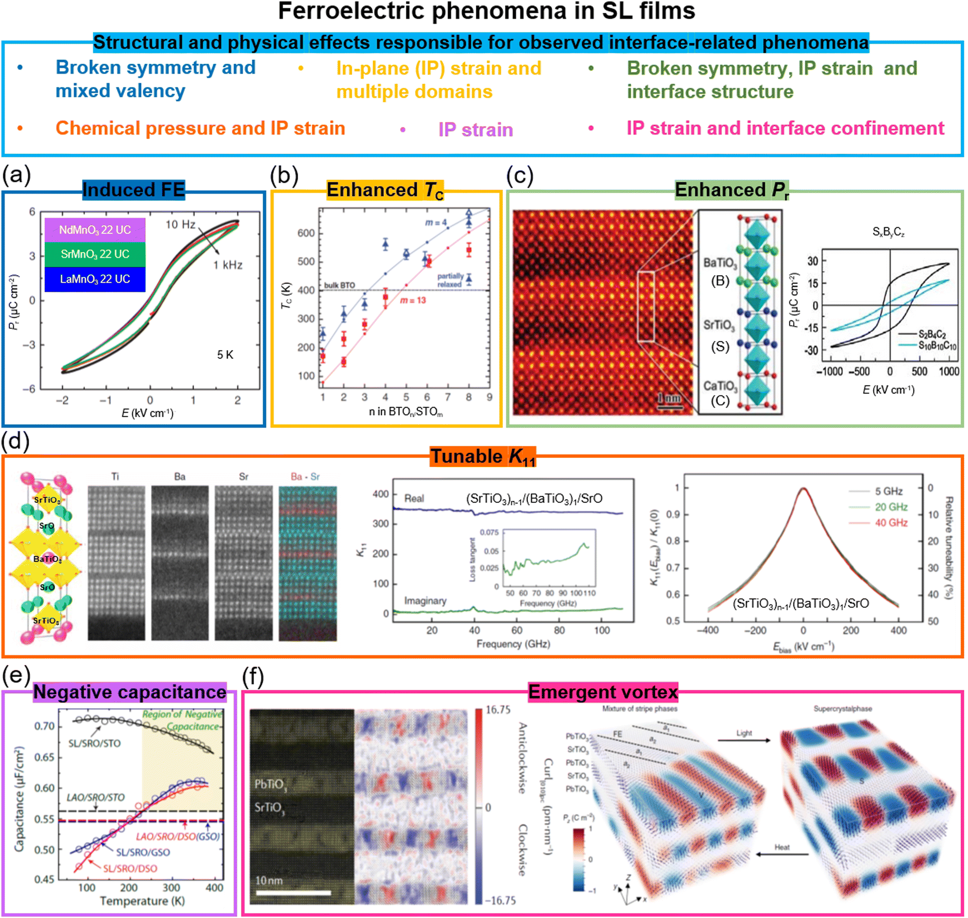 | ||
| Fig. 2 Ferroelectric phenomena in SL films. (a) P–E hysteresis loops measured from (NdMnO3)n/(SrMnO3)n/(LaMnO3)n superlattices. Reproduced with permission.41 Copyright 2012 Springer Nature. (b) FE TC in (BaTiO3)n/(SrTiO3)m superlattices as a function of n and m layer numbers. Reproduced with permission.23 Copyright 2006 AAAS. (c) Left panel: STEM image and diagram of (SrTiO3)x/(BaTiO3)y/(CaTiO3)z superlattices. Right panel: P–E hysteresis loops measured from (SrTiO3)2/(BaTiO3)4/(CaTiO3)2 and (SrTiO3)10/(BaTiO3)10/(CaTiO3)10 superlattices. Reproduced with permission.24 2005 Springer Nature. (d) Left: Schematic of crystal structure of (SrTiO3)n−1/(BaTiO3)1/SrO superlattices and STEM images the Ti, Ba, Sr and (Ba + Sr) elements. Middle: Real and imaginary parts of dielectric constant (K, the ratio of the material's permittivity ε to the permittivity of vacuum ε0) as a function of frequency for the n = 6 superlattice film. The inset shows the film loss tangent. Right: The ratio of K(Ebias, applied electrical field)/K(0, without applied electrical field) (left-hand axis) and relative tunability (right-hand axis) of the n = 6 superlattice film. Reproduced with permission.26 2020 Springer Nature. (e) Temperature dependent capacitance for superlattices grown on SrTiO3, DyScO3, and GdScO3 substrates. Reproduced with permission.28a Copyright 2014 American Chemical Society. (f) Left panel: STEM image of vortex structures formed in a (SrTiO3)10/(PbTiO3)10 superlattice. Reproduced with permission.29a 2016 Springer Nature. Right panel: Optical and thermal field control of the coexistence phase and superlattice phase. Reproduced with permission.42 2019 Springer Nature. | ||
No such emergent interface FE has been reported in VAN films to date. While it is certainly harder to grow such perfect vertical interfaces of desired compositions in VAN films, it is possible in some systems where the matrix film is highly similar in both structure and lattice parameter to the substrate.44 In fact, the effect has likely never been searched for, and is a fruitful avenue of future research, particularly in manganite-based VAN systems where mixed Mn valence is induced by the presence of oxygen vacancies. Indeed, interface structures in VAN systems predicted using DFT calculations show strongly distorted oxygen sublattices and higher oxygen vacancy concentrations.15b Hence, in a SrMnO3/CeO2 VAN film, interface-induced oxygen vacancies are anticipated. These would reduce some of the Mn4+ to Mn3+. Hence, it is possible that emergent FE could arise from this mixed valency in VAN films, just as in SL films. The signal would, in theory, be much higher than in SL films, owing to the higher density of interfaces. We note that a reduced overall cation valence at interface structures in VAN films would not be limited to manganites. Other transition metal oxides would also likely give mixed valent cation interfaces and hence wide-ranging novel interfacial properties. This is a rich area for future exploration.
Another proven route to inducing ferroelectricity in SLs is to induce octahedral rotations into a SL layer from another SL layer. This leads to hybrid improper ferroelectricity.45 It has been shown in perovskite SLs with the same B ions but different A (A and A′) ions, hence A/A′ SLs, e.g. LaGaO3/YGaO3. The octahedral rotations induce a sizeable polarization of 0.65 μC cm−2. This same effect would likely not be possible in VAN films, owing to the larger lateral pitch of the vertical structures, i.e. in the range 5–50 nm, rather than <1–3 nm as required here. We note also that ferroelectricity across the interfaces in the SLs is predicted to originate from charge transfer,46 charge order,47 and element intermixing.48 Similar effects are likely also taking place in VAN structures but, as far as known, have not been probed yet. This would be an interesting area of future research.
2.2 Enhanced ferroelectric TC and remanent polarization, Pr, in superlattice films
(BaTiO3)n/(SrTiO3)m SL with n = 1 (single unit cell thick BaTiO3) and m = 30 grown on (001) SrTiO3, with 2.3% lattice mismatch in the BaTiO3,23,49 gives a ferroelectric TC of 250 K,23i.e. lower than the bulk value of 403 K (Fig. 2b), which means the SrTiO3 is effective in straining the BaTiO3 and the atomically thick nature of the BaTiO3 does not seriously degrade the ferroelectricity. Furthermore, by tuning n and m, the TC of the BaTiO3 is increased up to 638 K. The higher-than-bulk TC arises from the strain effect applied to the BaTiO3 layers by the SrTiO3 (Fig. 2b).23 A similar approach, using thin ferroelectric and non-ferroelectric perovskite layers, has been applied to other FE SL combinations,50 both bilayers and even trilayers. A trilayer example is shown in Fig. 2c. Here x unit cells of SrTiO3, y unit cells of BaTiO3, and z unit cells of CaTiO3 (SxByCz) were grown on (001) SrTiO3 substrates.24 The strain in BaTiO3 layers is fully retained when its thickness does not exceed the combined thickness of the other layers. As a consequence, an overall 50% enhancement of the SL global remanent polarization, Pr, is achieved (Fig. 2c). Apart from the strain effect, the broken inversion symmetry and specific interface structure play unexpected roles in the enhancement of ferroelectric polarization. The broken inversion symmetry in three-component SLs has been used for investigating the ferroelectric ground states, the dielectric properties,51 and multiferroicity, as we discuss more in Section 4.As we show later, the TC in VAN films is highly tunable, and, just as for SL films, several hundred K TC enhancements are readily achievable. The biggest differences with SLs is the ease of growth of VAN films combined with the ability to maintain vertical strain to > micron thicknesses,21,25 whereas in SLs the total film thicknesses are only several 10's unit cells maximum. VANs are therefore more suited to actuator/energy harvesting/dielectric applications where larger volumes of material are needed, whereas SL films are more suited to Si-based electronics where charges at planar interfaces play an important role in switching for processor or memory applications.
2.3 Dielectric property enhancements in superlattice films
Owing to temperature/frequency-stable permittivity and dielectric tunability, dielectric materials are of interest in applications where device miniaturization and high-energy-density storage are needed.52 (Ba,Sr)TiO3 is an established compound that has been used in the development of tuneable dielectrics in microwave filters. There is no ferroelectric transition for pure SrTiO3 as it is paraelectric in bulk, but the ferroelectric TC is 403 K for BaTiO3. The TC is in between these values by varying the Ba:Sr ratio. However, charged pointed defects in (Ba, Sr)TiO3 thin films, notably oxygen vacancies, lead to increased dielectric loss.53
(SrTiO3)n−1(BaTiO3)1SrO SLs with n = 6 (single unit cell thick BaTiO3) (Fig. 2d) have lower dielectric loss than standard films. This is because the single unit cell thick BaTiO3 in the SL is under chemical pressure from the SrTiO3 layers. This likely reduces oxygen loss at the same time as increasing the tetragonality and hence also the ferroelectric polarization. Overall, at a temperature T = 300 K and an electric field E = 400 kV cm−1, a dielectric constant (K) tunability, i.e. the ratio of K(E)/K(0) (right panel in Fig. 2d), of around 46%, and a loss tangent (tanδ) of ∼0.06 were achieved at a 110 GHz frequency.26 Higher tunability values were achieved in much thicker (∼μm) VAN films (Section 6), i.e. dielectric constant tunability of up to 75% and tanδ of 0.01,27,54 although the frequency studied so far was lower than for SL films, at ∼1 MHz.
Another form of ferroelectricity in SLs has been demonstrated via improper ferroelectricity. In (PbTiO3)n(SrTiO3)m SLs with very short periods of n = 2 and m = 3, improper ferroelectricity55 is achieved resulting from strong competition between ferroelectric PbTiO339 and antiferrodistortive SrTiO356 distortions across the interface, causing antiferrodistortive rotations of the oxygen atoms in PbTiO3. In turn, a relatively high dielectric constant of 600 is achieved at 300 K and, from 300 K to 550 K, the dielectric constant is independent of temperature. No improper ferroelectricity has been observed in VAN films to date but there is the possibility to observe it in the most perfect VAN structures. The PbTiO3/SrTiO3 VAN system would be a good starting point. While phase intermixing between PbTiO3 and SrTiO3 could occur in the VAN films, there is precedent for lack of mixing between similarly lattice matched perovskite VAN materials.57 Thus for PbTiO3/SrTiO3 VAN, a similar situation could come about. Less (or no) mixing compared to the bulk thermodynamic case related of the role of epitaxy at the substrate film interface. Hence pure SrTiO3 on SrTiO3 is the lowest interfacial energy situation and may prevent intermixing with Pb. More experiments and calculations are highly required to confirm this possibility.
2.4 Negative capacitance and emergent polar vortex in superlattice films
The negative capacitance effect in ferroelectrics occurs when there is a negative differential capacitance around a zero charge level. Hence, an increase in charge in the ferroelectric occurs when the voltage is decreased. This effect could reduce the subthreshold swing in a conventional transistor below the otherwise minimum limit of 60 mV decade−1.28a,58 Negative capacitance in SL films of ferroelectric Ba0.8Sr0.2TiO3/dielectric LaAlO328a has been shown with the capacitance enhancement level tuned by epitaxial strain via the growth of SLs on three different substrates (Fig. 2e). Furthermore, in PbTiO3/SrTiO3 SLs a direct measurement of steady-state negative capacitance has shown that local regions of negative capacitance emerge at domain walls, where the energy density is larger than that in the bulk of the domains and the polarization is suppressed.58aAnother novel phenomenon observed recently in PbTiO3/SrTiO3 SLs is the formation of polar vortices in PbTiO3. In fact, ferroelectric vortex states were theoretically predicted in nanostructures,59 but not observed in thin films until 2016. Long-range and chiral ferroelectric vortex structures have been observed in PbTiO3 in (PbTiO3)n/(SrTiO3)n SLs with n = 10 (left in Fig. 2f).29a A combination of substrate induced strain and confinement from the SrTiO3 layers produces the effect leading to a clockwise vortex-like pattern, paired with every other vortex in an anti-clockwise manner. The coexistence phase of ferroelectric a1/a2 domains and vortex states can be transferred to a single 3D SL phase by optical and thermal manipulation (right in Fig. 2f).42 Room-temperature polar-skyrmion bubbles have further been observed in these SL systems,28b giving the possibility of highly efficient skyrmion memory.
There have been no such reports thus far of polar vortices in VAN films. However, the ∼5 nm length scales, strain and confinement effects involved in the above SL example, can also be readily achieved in VAN films, even in the PbTiO3/SrTiO3 system. Hence, PbTiO3 pillars should form in a SrTiO3 matrix when the film is grown on SrTiO3. The Pb and Sr would be unlikely to mix based on the differing ion sizes and charges, and also because it would not be preferred because pure SrTiO3 forms a perfect epitaxial match on SrTiO3. Thus, it may be possible to achieve few nm sized nanopillars of PbTiO3 as can be achieved in other VAN systems60 and thus create vertical polar skyrmions throughout the whole film thickness.
3. Magnetic phenomena in superlattice films
Similar to ferroelectric oxide thin films, magnetic oxides, notably transition metal oxide (TMO) perovskites, have potential applications for data storage and non-volatile random-access memory. Strong magnetization, high TC, and perpendicular anisotropy are highly desired for such applications. A broad range of functionalities arising from the interplay between the interconnected degrees of freedom of the magnetic spins, lattice structure, bonding orbitals and ionic charges, mediated by corner-shared BO6 units octahedra which can tilt around three orthogonal axes61 can be exploited and manipulated in SLs.At SL interfaces, the following effects have been shown: the enhancement of TC, modified electronic conduction, induced ferromagnetism from non-ferromagnetic layers, exchange bias, magnetic anisotropy, and topological Hall effect, etc. (Fig. 3). In Section 7, we discuss the comparative magnetic effects in VAN films.
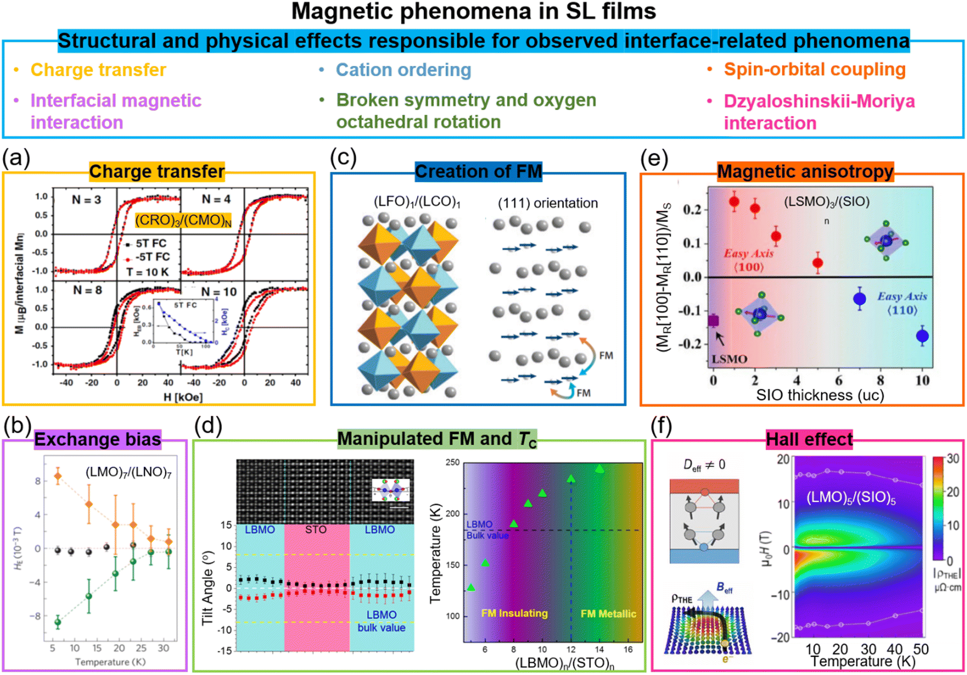 | ||
| Fig. 3 Magnetic phenomena in superlattice films. (a) Magnetic hysteresis loops of (CaRuO3)3/(CaMnO3)N superlattices. Reproduced with permission.30 Copyright 2012 American Physical Society. The inset shows the temperature dependent HC and HEB for (CaRuO3)3/(CaMnO3)8. (b) Temperature dependent HE for (LaNiO3)7/(LaMnO3)7 superlattices after field-cooling in a +0.4 T field (green circles) and in a −0.4 T field (orange diamonds). Reproduced with permission.62 Copyright 2012 Springer Nature. (c) Schematic diagram of (LaFeO3)1/(LaCrO3)1 superlattices grown on (111)-oriented substrates and the resultant spin structures. Reproduced with permission.63 Copyright 2014 Annual Reviews. (d) Left panel: STEM image (top) and octahedral tilt angles (bottom) of (La0.9Ba0.1MnO3)8/(SrTiO3)8 superlattice. Right panel: Ferromagnetic TC as a function of layer thickness in (La0.9Ba0.1MnO3)n/(SrTiO3)n superlattices. Reproduced with permission.64 Copyright 2020 Wiley-VCH. (e) Magnetic anisotropy of (La0.7Sr0.3MnO3)3/(SrIrO3)n superlattices as a function of SrIrO3 layer thickness. Reproduced with permission.65 Copyright 2016 PNAS. (f) Left panel: Schematic diagram of the topological Hall effect originating from the Berry phase and a chiral spin texture. Right panel: The topological Hall resistivity of the (LaMnO3)5/(SrIrO3)5 superlattice. Reproduced with permission.37 Copyright 2020 AAAS. | ||
3.1 Magnetic interactions across interfaces involving 3d TMO superlattice films
Exchange bias (EB) has been induced in SLs via two different effects. First, charge transfer (to equilibrate the differing chemical potentials of carriers in the materials on either side of the interface) occurs in many oxide SLs and leads to new electronic and magnetic states.66 For example, in (CaRuO3)3/(CaMnO3)N SLs composed of the antiferromagnetic insulator CaMnO3 and the paramagnetic metal CaRuO3, an exchange bias as high as 3 kOe is induced at 10 K (Fig. 3a).30,67 Here, a ferromagnetic interface is created in one unit cell, because of the double exchange interaction in the CaMnO3 at the interface where Mn4+ is partially reduced to Mn3+ because of electron transfer from CaRuO3 to CaMnO3. The consequent ferromagnetic/antiferromagnetic coupling across the interface creates the exchange bias effect.Exchange bias is also achieved in (111)-oriented LaMnO3/LaNiO3 (ferromagnetic/paramagnetic) SLs (Fig. 3b). Here, interfacial interactions, e.g. quantum confinement effects,68 induce a complex magnetic structure in a non-magnetic material. Hence, magnetism resembling a spin density wave in the paramagnetic LaNiO3 layers in contact with the ferromagnetic LaMnO3 is created.62 An exchange bias as high as 90 Oe is induced at 5 K. Large vertical exchange bias effects have been demonstrated at much higher temperatures in VAN films, namely at room temperature, and the reasons for this are discussed in Section 7.
Similar to the (CaRuO3)3/(CaMnO3)n SLs, in (LaMnO3)2n/(SrMnO3)n SL, a metallic ferromagnetic state emerges at the interface from the parent materials which are not ferromagnetic, namely an antiferromagnetic Mott insulator (LaMnO3),69 and a band insulator with G-type antiferromagnetism (SrMnO3).70 Again, interfacial charge transfer between Mn3+ and Mn4+ cations is responsible for emergent FM, i.e. electrons ‘leak’ from the Mn3+ in LaMnO3 into the Mn4+ in SrMnO3.70,71 The metallic state is apparent for n ≤ 2 (when the occupied Mn eg electrons spread over the entire lattice), but for higher n, the bulk of the film (insulating antiferromagnetic) dominates the properties.
Emergent ferromagnetism and metallicity should also be easily achievable in VAN films, as charge transfer across interfaces is not restricted to planar interfaces. To date, in several VAN systems interesting additional magnetic and conducting effects have been observed (separate to the expected contributions from the bulk properties to the film).15a,72 However, the origins of these effects, whether they be from charge transfer effects, orbital reconstructions, etc., have not been widely explored. Further studies of such effects in perfectly aligned VAN structures, including understanding of the phenomena using high resolution microscopic and scanning probe tools to probe the structures and interface charge states is a fruitful area of future research. Also, since the vertical interfaces in VAN films intersect the film surface, the conducting properties of VAN interfaces are readily measurable giving an advantage over SL where interfaces are buried.73
Another mechanism to induce ferromagnetism at interfaces is by tuning the relative fractions of B–O–B, B–O–B′, and B′–O–B′ bonds, In (ABO3)/(AB′O3) SLs, there are different magnetic exchange interactions couplings across the interfaces for different orientation films. Hence, different spin structures have been observed for (LaFeO3)1/(LaCrO3)1 SLs grown on (001)-, (110)-, and (111)-oriented SrTiO3 substrates.32a,74 As shown in Fig. 3c, based on Anderson, Goodenough, and Kanamori rules, ferromagnetic exchange interactions across Fe–O–Cr bonds can be realized in the (111)-oriented SL films. A high TC of 375 K and high interfacial magnetization of 2.5μB were achieved in (111)-oriented (LaFeO3)1/(LaCrO3)1 SL.
A further interfacial phenomenon which induces modified interfacial properties in magnetic perovskite SLs is orbital reconstruction. This occurs when TMO thin films are strained leading to different BO6 octahedral rotations.61,64 For example, the ferromagnetic TC in La2/3Sr1/3MnO3 is significantly enhanced from 370 K in bulk La2/3Sr1/3MnO3 to 650 K in (La2/3Sr1/3MnO3)3/(BaTiO3)3 SLs owing to straining of the La2/3Sr1/3MnO3 by BaTiO3.75 The change of the Mn orbital occupation from dx2−y2 within the film to d3z2−r2 at the interface is responsible.
A further mechanism for tuning the magnetic coupling within SL layers containing magnetic moments is via non-trivial oxygen octahedral coupling (OOC) across the heterointerfaces which produces different BO6 octahedral rotations in the layer of interest.61c,76 For instance, in non-magnetic (LaMnO3)n/(SrTiO3)n SLs, magnetisation was induced in the interfacial layers in LaMnO3 with a maximal saturation magnetization of 2.97μB per Mn for the n = 6 SL film.77 It should be noted that while interactions between layers in the films lead to the modulation of BO6 octahedral rotations, epitaxial strain also play an important role. To largely eliminate the strain effect, (La0.9Ba0.1MnO3)n/(SrTiO3)n SLs were studied,64 where there is only 0.2% strain between the La0.9Ba0.1MnO3 and SrTiO3. It was possible to engineer the BO6 octahedral rotations up to 12 unit cells, larger than previous reports by 6 unit cells. Consequently, the out-of-plane Mn d3z2−r2 orbitals became occupied, the Mn eg bandwidth reduced, a ferromagnetic insulating state in La0.9Ba0.1MnO3 created, and TC enhanced to 235 K from 185 K in bulk (Fig. 3d).
As already noted, in SL films the substrate plays a role in controlling the perovskite octahedral rotations and oxygen octahedral coupling. The substrate exerts strain on the film which induces octahedral rotations in the film, but there is also coupling of the film octahedra to substrate octahedra. The question is whether similar interface coupling effects could be created in VAN films but without the interference from the substrate as is the case of SL films. In fact, in VAN the substrate influence is weak above around 20 nm film thickness and since micron thick films are relatively easy to grow and indeed preferred for VAN, any coupling effects across the vertical interfaces in VAN are largely independent of the substrate. On the other hand, as shown in Table 1, the challenge for VAN is creating highly faceted interfaces which are also perpendicular to the substrate without meandering. As already noted, this is highly possible when the matrix material is the same as the same or a very closely lattice and structurally matched material as the substrate material, e.g. SrTiO3-based VAN film on SrTiO3 substrate,54 and hence there is wide scope for exploring new interface coupling effects in VAN films with the most ideal interfaces.
3.2 Magnetic interactions across interfaces involving in 5d TMO superlattice films
SLs containing perovskites with strong spin–orbit coupling have been investigated to further explore new interface coupled effects and exotic magnetic reconstructions. For example, in SrMnO3/SrIrO3 superlattices,78 where SrMnO3 is the 3d antiferromagnetic insulator and SrIrO3 is a 5d paramagnetic metal, there is charge transfer of ∼0.5 electrons per unit cell from SrIrO3 to SrMnO3. Hence, there is induced ferromagnetism in the SrMnO3 which is normally antiferromagnetic.79 In addition, the strong spin–orbit coupling also leads to perpendicular magnetic anisotropy (PMA) and a large anomalous Hall effect. Furthermore, in La0.7Sr0.3MnO3/SrIrO3 (ferromagnetic metal/paramagnetic metal) SLs,65 magnetic coupling across the interfaces produces an emergent weak ferromagnetism in the SrIrO3 layers. Also, since magnetocrystalline anisotropy is closely linked to spin–orbit coupling, the in-plane magnetic anisotropy of La0.7Sr0.3MnO3 was changed by varying the thickness of the SrIrO3 (Fig. 3e). A PMA constant (Keff) of 4 × 10⁶ erg cm−3 was further optimised by increasing the doping level, x, in the La1−xSrxMnO3/SrIrO3 SLs.35Broken inversion symmetry and strong spin–orbit coupling in 3d–5d interfaces can also lead to large chiral Dzyaloshinskii–Moriya interactions (DMIs), inducing non-trivial spin textures, i.e. topological phenomena. In LaMnO3/SrIrO3 SLs (Fig. 3f), a highly robust chiral magnetic phase with large topological Hall effect (THE) of 75 μΩ cm was observed.37 The present research on the interfaces with iridate oxide systems is still in infancy, and many open and intriguing questions still remain to be explored.
Finally, we note that the skyrmion structures formed in SrIrO3 superlattices incorporate insulating or metallic layers are formed in films of only 2–8 unit cells (or 1–4 nm) thickness.37,80 Thus, as mentioned for the polar skyrmions in Section 2.4, it is highly possible to grow VAN structures of this dimension and potentially grow, by self-assembly, skyrmion SrIrO3 columns in a film matrix, the route for growing perovskite nanocolumns in VAN films having already been demonstrated in several systems, e.g. BiFeO3, BaTiO3, and Ba1−xSrxTiO3 systems.25 Indeed, it is possible that SrIrO3 would grow more readily in VAN films compared to plain epitaxial films. This is because the phase could be stabilised using vertical epitaxy with a matrix phase in the VAN film.19b Also, to maintain stoichiometry of the SrIrO3, a matrix material containing either or both Sr and Ir species could be used so as to produce a source material to prevent loss of these volatile cations during growth.
4. Multiferroism and magnetoelectricity in superlattice films
Materials that exhibit simultaneous order in their electric and magnetic ground states are promising for enabling electric field control of magnetism via the CME effect. Such materials are rare, however, due to the contradicting requirements of empty d orbitals via cation off-centering required for ferroelectricity and partially filled d orbitals for magnetism.81 Creating composite systems where the properties of two different systems are coupled across their interface is a potential way to create artificial multiferroics. Oxide SLs are one form of composite system. As we discuss below, when two systems are coupled via an interface in SLs comprising magnetic and ferroelectric layers, proximity effects, broken inversion symmetry, strain and defects, and geometric frustration and strain engineering can give rise to either multiferroism (at least two ferroic properties in one materials systems) and/or artificial magnetoelectricity (electric field control of magnetism or vice versa). We note that while there have been many predictions of the aforementioned effects in a range of SLs82 not many have been experimentally verified. On the other hand, there have been interesting experimental observations in SLs not predicted by theory, typically using combinations of a perovskite which exhibits ferroelectricity, with another which exhibits some form of magnetic order.Two key examples of multiferroism induced in SLs are in La2/3Sr1/3MnO3/BaTiO3 (non-polar-tilt ferromagnet/polar ferroelectric) and La2/3Sr1/3MnO3/BiFeO3 (non-polar-tilt ferromagnet/ferroelectric antiferromagnet). In the first case (Fig. 4a), due to proximity effects a structural phase transition from non-polar to unconventional polar (hence giving both ferroelectricity and ferromagnetism, thus multiferroicity) was induced in ultrathin 4-unit-cell La2/3Sr1/3MnO3.83 In the second case, magnetism (up to 200 K) was induced in ultrathin 5-unit-cell ferroelectric BiFeO3,87 to a level of 1.83 ± 0.16μB per Fe, increased from 0.03μB per Fe in bulk BiFeO3, and attributed to strong orbital reconstruction between Fe and Mn across the interfaces.
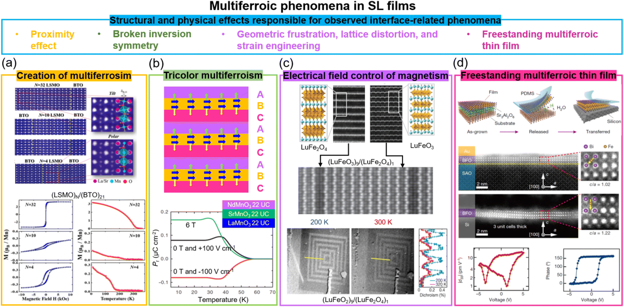 | ||
| Fig. 4 Multiferroic phenomena in SL films. (a) Top panel: STEM images of (La2/3Sr1/3MnO3)N/(BaTiO3)21 superlattices. Bottom panel: M vs. H loops (left) and M vs. T curves (right) for (La2/3Sr1/3MnO3)N/(BaTiO3)21 superlattices. Reproduced with permission.83 Copyright 2017 PNAS. (b) Top panel: A tricolor superlattice for designing the multiferroicity. Reproduced with permission.84 Copyright 2007 Elsevier. Bottom panel: Temperature dependent polarization measured under electrical and magnetic field for NdMnO3/SrMnO3/LaMnO3 superlattices. Reproduced with permission.41 Copyright 2012 Springer Nature. (c) Top panel: STEM images of end-members LuFe2O4 (left) and LuFeO3 (right); middle panel: (LuFeO3)9/(LuFe2O4)1 superlattice. Bottom panel: XMCD PEEM images of (LuFeO3)9/(LuFe2O4)1 superlattice measured at 200 K and 320 K. Reproduced with permission.85 Copyright 2016 Springer Nature. (d) Top panel: Schematic of growth and transfer of a freestanding thin films. Middle panel: STEM images of 3-unit-cell BiFeO3 film before and after etching Sr3Al2O6 layer. Bottom panel: Piezoelectric properties of 4-unit-cell BiFeO3 film after etching Sr3Al2O6 layer. Reproduced with permission.86 Copyright 2019 Springer Nature. | ||
The creation of ferroelectricity, multiferroicity, and a DME effect has been achieved through simultaneous breaking of time-reversal and spatial-inversion symmetries in “tricolour” ABCABC SLs composed of three sequential kinds of perovskite layers88 (top plot in Fig. 4b). The polarization at the AB (or BC) interfaces has the same sign leading a non-vanishing toroidal moment equivalent to a built-in vector potential under the presence of spin–orbit coupling, thereby producing ME coupling. For example, a ferroelectric TC of 40 K was achieved in NdMnO3/SrMnO3/LaMnO3 SLs, even though individual layers have no polar moment. Also, ME coupling was achieved by magnetic modulation of the polarization (bottom plot in Fig. 4b).41 Density functional calculations show that the combination of broken space inversion symmetry and the presence of Mn3+/Mn4+ mixed valence, arising from cationic asymmetry and interfacial polar discontinuity, produce emergent ferroelectric and ME coupling. However, the interface-induced ME coupling is very weak and occurs below 55 K.
Other works on creating magnetoelectricity in SLs have centred around a wide range of SL combinations, e.g. in BaTiO3/BiFeO3 (ferroelectric/ferroelectric and antiferromagnet) SLs a direct ME coefficient αME up to 55 V cm−1 Oe−1 at 300 K was measured,38b higher than in single-phase BiFeO3 (αME = 4.2 V cm−1 Oe−1), which was explained by the diffusion of Ba and Ti into the BiFeO3 layers. Hence, the influence of unwanted chemical intermixing across the interface and impurities buried within superlattices is uncertain.
Another different mechanism to achieve multiferroicity and ME coupling was demonstrated using symmetry breaking across a SL interface of (LuFeO3)m/(LuFe2O4)1. Rumpling (periodic buckling of lattice planes) in LuFeO389 imposed a local distortion in one unit cell LuFe2O4, thus removing the mirror symmetry in the LuFe2O4 and enabling ferroelectricity to emerge in this ferrimagnetic phase85 (Fig. 4c). The ferrimagnetic TC of the LuFe2O4 was increased from 240 K to 281 K because of a local distortion applied by LuFeO3. Since the ferroelectric order couples to the ferrimagnetism, electrical field control of magnetism, as measured using X-ray magnetic circular dichroic photoemission electron microscopy (XCMD PEEM), was achieved at 200 K (Fig. 4c). The clamping of the films to the substrate or leakage effects possibly limit macroscopic measurements using electrodes applied across the whole film.
Finally, we note that there has been more success in achieving direct ME (DME) in all-metallic systems90 than in oxides. An example is (Ta/Cu/IrMn/FeCoSiB)n/AlN/Si,90c where a relatively large direct ME effect of 96 V cm−1 Oe−1 was observed at 300 K. However, the requirement to use precious metal Ir, the need to use a relatively complex stack of layers, and no observation of CME, are limiting factors for this system. Hence, arguably, there is more promise for oxide systems, although controlled interface composition and structure, and the elimination of substrate clamping effects are important areas of future study. The latter effect prevents intrinsic displacement of ferroelectric and magnetostrictive materials.
Very promisingly, in recent years much progress has been made with lift-off and transfer of films to practical substrates.86,91 As far as known, the transfer process has not been applied to multiferroic SL films but it has been used for single layer films and it is expected that multiferroic SL films would behave similarly. The advantage of lifting off a multiferroic SL film is that it would be free from substrate clamping. This could enable strain coupled magnetoelectricity to be realised. Fig. 4d shows an example of using water-soluble Sr3Al2O6 as the sacrificial buffer layer to produce freestanding BiFeO3 multiferroic thin films with a high crystalline quality that can be fabricated down to one unit cell. Also, robust and switchable ferroelectric polarization was demonstrated for a four unit-cell, transferred BiFeO3 film on Si, as confirmed by STEM and piezoelectric measurements, respectively. We note that VAN films have also been successfully lifted-off and transferred to Si. Owing the nanoscale nature of VAN films, they appear to be more resistant to crack propagation yielding a higher success rate of film transfer compared to plain films.92 More work is needed to explore the performance of lifted-off ferroic and multiferroic VAN films.
Contrasting with much of the SL work describe above, artificial multiferroic effects in VAN films have not focused on purely interfacial phenomena, but on more macroscopic effects caused by strain coupling of phenomena across vertical interfaces which take effect in the whole body of film. An advantage of VAN films over SL is the lack of a substrate clamping effect. On the other hand, leakage currents can be problematic if the right combinations of materials are not used. Strategies for overcoming the leakage while also boosting interface coupling are discussed for VAN multiferroics in Section 8.
5. Summary of ferroic phenomena in superlattice films
Overall, artificial SLs of complex oxides for ferroics are systems which provide an excellent platform for fundamental research, allowing the validity of theoretical predictions to be probed, new science to be revealed, and the realization of new materials with tailor-made properties. On the other hand, SLs also have challenges as interfaces can be subject to intermixing effects and defect formation which are hard to probe and identify. Promisingly, improvements in tools to understand interfaces are improving rapidly, there are also continuous advances in growth tools. Hence, SL films continue to have huge promise for next generation electronics.B. Vertically aligned nanocomposite (VAN) films
6. Ferroelectric phenomena in VAN films
In SL films (discussed in part A above), it has been demonstrated that ferroelectricity can be induced from interfacing non-FE materials, and also that fascinating effects such as negative capacitance and polar vortices can be created. As already noted, such phenomena have not yet been observed in VAN films (Table 2). On the other hand, a number of other structural effects (Table 1) give rise to fascinating phenomena in VAN films. In particular, novel strain effects play a strong role in determining functional properties.We recall that in standard planar SL ferroelectric films, epitaxial strain from the underlying substrate is often used to tune properties.1e,24,93 However, this substrate-induced interfacial strain can only extend to tens of nanometers thickness and hence the TC enhancement is largely confined to the interfacial region. It has been shown in epitaxial perovskites that from above the first tens of nanometers thickness up to ∼100 nm, the strain is relieved by a range of crystalline defects to compensate the strain.94 Such defects can degrade the functionality of epitaxial perovskite devices which exploit the functionality of the whole film rather than just the interface, e.g. a strain-enhanced-TC ferroelectric actuator. In VAN films, on the other hand, by incorporating stiff nanopillars into a ferroelectric matrix large vertical strains (of >1%) can be induced throughout the whole film and hence the thickness-limiting substrate strain effect is not relied upon.21 This enables wide-ranging ferroelectric property tuning in micron thick films. Since the lateral distance between the nanopillars is typically only ∼20 nm, the strain is not relaxed to a large extent as for epitaxial films, and so the film perfection and crystallinity remains high for 100s nm thick VAN films.13,95 Hence, enhanced TC, remnant polarization, retention, dielectric tunability, and reduced loss tangent and leakage current are achieved.25,27,54,96
In section A, we presented several examples of VAN compositions that could be explored to try and mimic and also new opportunities the exciting emergent effects achieved in SL films. In the following sections we focus on VAN films. Before, we go into details of each of the enhanced properties, explaining how the strain in VAN films contributes to these properties, we first consider how research on SLs could benefit from VAN research. A key processing advantage of the VAN approach over SL is it is relatively fast and simple for exploring new combinations of materials and their interfaces. Hence, VAN can serve as fast screening method to predict which phases and which ratios of phases could also give rise to novel interface related functionalities in SL structures. For example, in Section 8, we show how a triple VAN system enables a self-biased magnetoelectric to be achieved. For SL films, it would take longer to explore the right thicknesses of the layers to use, to be sure there are no interface mixing effects, and also to know if the magnetoelectric effect were present (as it could obscured by substrate clamping effects). Hence, with the knowledge gained from VAN, SL films of the demonstrated compositions could now be tested, and films lifted off to remove any clamping effects.
6.1 Enhancement of ferroelectric TC, remanent polarization, Pr, piezoelectric d33 and retention in VAN films
The first demonstration of enhanced ferroelectricity using VAN was in ∼2 micrometre-thick BaTiO3-based VAN films embedded with stiff Sm2O3 pillars yielding a >2% vertical extension in the BaTiO3. While many BaTiO3 applications are limited by its relatively low TC (∼396 K),98 here in the VAN films a TC up to ∼970 K (higher also than the 638 K achieved in BaTiO3/SrTiO3 SL99) can be achieved which opens up many more applications possibilities.21 Other BaTiO3-based and SrTiO3-based VAN films have also shown strong enhancements with TC enhanced (Fig. 5a) and leakage current reduced.54,96c,100 We note that reduced leakage is not universal for VAN films but depends on whether the interface is in tension or compression,72b the nature of the interface structure(s) that form in the VAN film to minimise interfacial energy,73b the nature of the transition metal cations and their redox equilibria, and whether a rectifying p–n junction forms between the film and substrate.40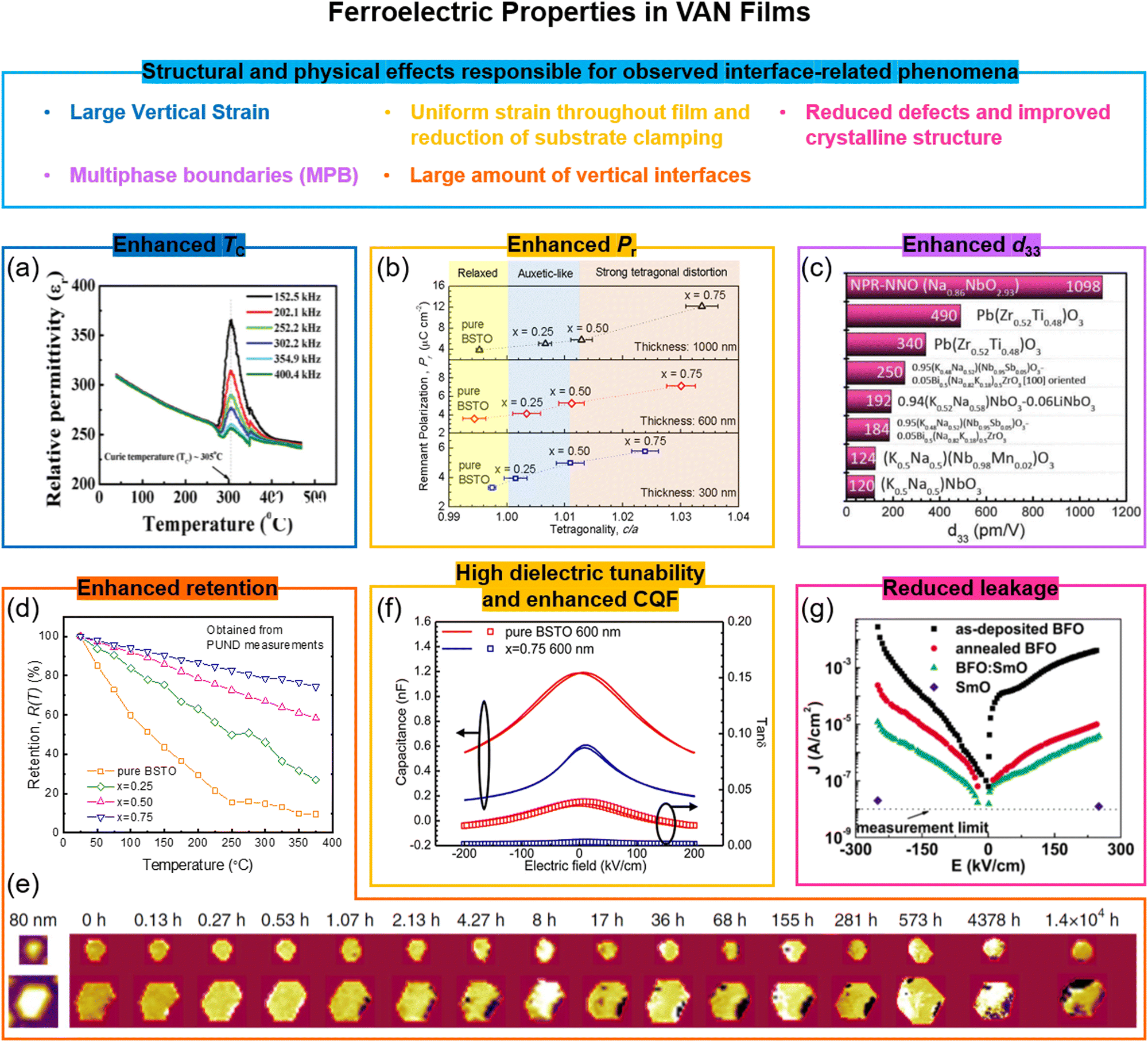 | ||
| Fig. 5 Enhanced ferroelectric properties achieved using VAN structures. (a) Cross-sectional TEM image of SrTiO3–Sm2O3 VAN; (b) remnant polarization of (Ba,Sr)TiO3–Sm2O3 VAN film as a function of the tetragonality of (Ba,Sr)TiO3 phase. Reproduced with permission.25 Copyright 2017 Wiley-VCH. (c) Giant piezoelectric Na-deficient NaNbO3–NaNbO3 (NPR-NNO) VAN film. Reproduced with permission.97 Copyright 2020 AAAS. (d) Comparison of normalized retained polarization versus temperature for a pure (Ba,Sr)TiO3 film and for (Ba,Sr)TiO3–Sm2O3 VAN films with different Sm2O3 contents (x). Reproduced with permission.25 Copyright 2017 Wiley-VCH. (e) The evolution of polarisation retention in a FE domain of a BiFeO3 (111) mesocrystal with time. Reproduced with permission.96b Copyright 2016 Springer Nature. (f) High tunable relative permittivity, εr, as shown by the large change in capacitance value with electric field in a (Ba,Sr)TiO3–Sm2O3 VAN film, measured at 1 MHz. An enhanced commutation quality factor (CQF) is also achieved. Reproduced with permission.27 Copyright 2012 American Chemical Society. (g) Reduced leakage current of a BiFeO3–Sm2O3 VAN film compared to plain BiFeO3 or plain Sm2O3 films. Reproduced with permission.96a Copyright 2008 AIP Publishing. | ||
As shown in Table 2, similar ferroelectric property enhancements are only achievable in planar or SL films if they are ∼10's nm thick or less.93a Such high TCs in micron thick films are necessary for advanced device applications, such as the electrocaloric devices,101 actuators,102 and microwave tuneable filters,53a and cannot be achieved in planar films.
The remnant polarization (Pr) has also been systematically increased using (Ba,Sr)TiO3-based VAN structures (Fig. 5b), both by increasing the fraction, x, of nanopillars and increasing film thickness (to ∼μm's),25 both of which increase the film tetragonality. The Pr values are about ∼3× larger compared to (Ba,Sr)TiO3 planar films (Table 1). A near doubling of Pr has also been shown in BaTiO3–NiO VAN films.103 A giant enhancement of piezoelectric response is also possible in VAN films (Fig. 5c). Liu et al.97 showed in nanopillar-like sodium-deficient NaNbO3 VAN a piezoelectric coefficient d33 of ∼1098 pm V−1, which compares to ∼22 pm V−1 for stoichiometric NaNbO3 films. The TC of the VAN film is ∼723 K, which is similar to that of the stoichiometric NaNbO3 film. Local heterogeneity of sodium-deficient NaNbO3 and stoichiometric NaNbO3 phases was deemed to be responsible.
Temperature-dependent and time-dependent changes of the polarization state of ferroelectric films, i.e. thermal and temporal retention, are of great importance for non-volatile nanoelectronic devices based on ferroelectrics,25,96b,104e.g. for above-room temperature-operation, high-stability memory devices. The retention parameters are sensitive to film thickness and microstructure, electrodes, etc.105 Much enhanced thermal and temporal polarization retention has been demonstrated in (Ba,Sr)TiO3–Sm2O3 and CoFe2O4–BiFeO3 VAN films (Fig. 5d and e) compared to the pure film counterparts of (Ba,Sr)TiO3 and BiFeO3, respectively. Ultra-dense vertical interfaces lead to a strong tetragonal distortion and vertical ferroelectric domains25,96b which are ‘pinned’, thus retarding relaxation processes.
6.2 Dielectric property enhancements and reduced leakage in VAN films
Stemming from the increased tetragonality induced in the ferroelectric phase, dielectric properties are enhanced in VAN films.27 In (Ba,Sr)TiO3-based VAN films, a tunability of 75% (200 kV cm−1 field), and a low dielectric loss of 0.01 was achieved at room temperature, in contrast to the respective values of ∼52% and 0.06 in pure (Ba,Sr)TiO3 films27 (Fig. 5f). Critically, the loss is reduced when the tunability is enhanced which is opposite to planar films and results from the unusual strain states in VAN films.13 The combination of high tunability and low loss lead to a high communication quality factor (CQF) value. In SrTiO3-based VAN films, a record communication quality factor (CQF) of up to 3300 was achieved which gives the system strong potential for tuneable RF applications.54Leakage is a long-standing problem in ferroelectric oxide thin films, commonly caused by oxygen deficiency and the presence of point or line defects. As already mentioned above, leakage can be reduced using VAN films. Taking the example of BiFeO3, a promising candidate for multifunctional non-volatile memory devices because of the coexistence of both the antiferromagnetic order with Néel temperature (TN) of 643 K106 and ferroelectric order with TC of 1123 K,107 leakage from a range of defects is common and can give either p-type or n-type behaviour.108 In BiFeO3-based VAN films, the leakage was reduced by several orders (Fig. 5g).72a,96a This was ascribed to the compressive out-of-plane (OOP) strain of −1.46% that was induced in the BiFeO3, induced by the embedded nanopillars. It was postulated that such a compression would reduce the oxygen vacancy concentration and hence carriers associated with these vacancies.109 However, some chemical intermixing, leading to doping of Sm into the BiFeO3 could also contribute to the lowering of the leakage. Of course, not all VAN films can have judicious compression engineered into them as for this BiFeO3 example.
6.3 Exploiting both bulk and surface effects for property enhancements using VAN
One key advantage of VAN films over SL or standard films is the ability to create very high surface area structures from them, and at the same time to retain strong ferroic properties even after treating them by chemical etching. Such etching removes the pillar phase in the VAN rendering a mesoporous film. There are many potential applications which could benefit from mesoporous films with tubular pores from the etched nanopillars, having high surface area for chemical, gas, or biological sensing, or even filtration (especially because the pore size is tunable via growth parameters and VAN film composition). Adding in ferroicity to the mesoporous film could enable greater sensitivity or tunability of the device performance/operation.One example of the benefits of mesoporous VAN is the doped/undoped SrTiO3–MgO VAN film system. Here, the MgO is chemically etched out of the film, leaving a mesoporous SrTiO3 matrix (Fig. 6a) with the out-of-plane tensile strain in the SrTiO3 matrix largely intact. More understanding of the mechanisms and universality of matrix strain retention after etching pillars out of the VAN films is required. This mesoporous matrix leads to photoelectrochemical (PEC) water splitting compared to literature (Fig. 6b and c),110 arising from (a) an order of magnitude larger surface area for light absorption, (b) optimised carrier concentration from Ag and Nb of the doped SrTiO3,111 and (c) above-room-temperature ferroelectricity from the vertical strain effect induced by the VAN structure, which produced a reduced flat-band potential and enhanced charge extraction (Fig. 6d–f)110,111
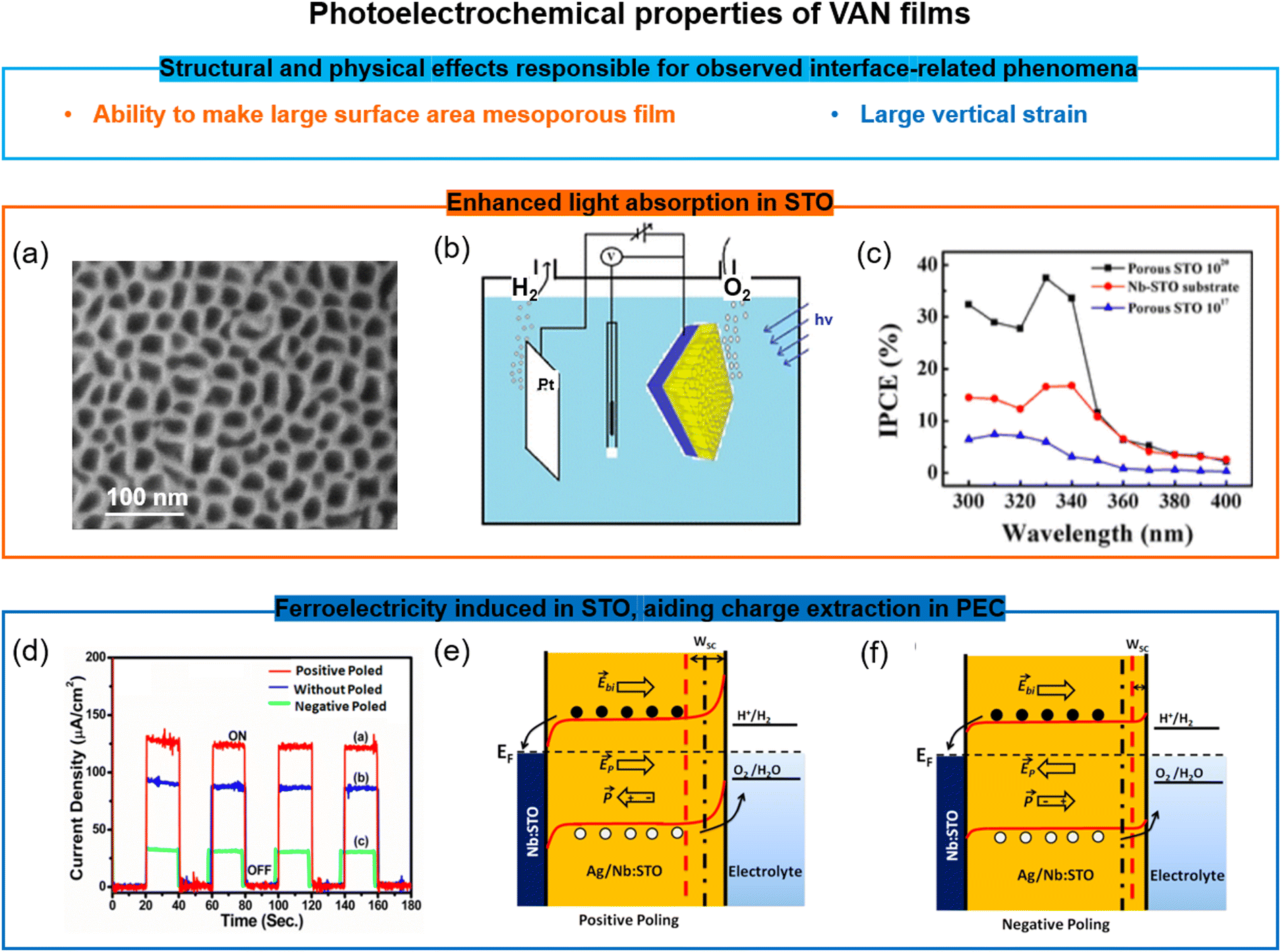 | ||
| Fig. 6 Doped/undoped SrTiO3-based VAN porous ferroelectric films for water splitting applications. (a) SEM image of the surface of a undoped mesoporous SrTiO3 film. Reproduced with permission.110 Copyright 2016 American Chemical Society. (b) Schematic of the water-splitting by the undoped mesoporous SrTiO3 film. Reproduced with permission.110 Copyright 2016 American Chemical Society. (c) Enhanced incident photon to current efficiency (IPCE) in the undoped mesoporous SrTiO3 film compared to both a continuous SrTiO3 film and the Nb-doped SrTiO3 substrate. Reproduced with permission.110 Copyright 2016 American Chemical Society. (d) The photoelectrochemical (PEC) response of a mesoporous (Ag,Nb)-co-doped SrTiO3 film at different polarization states. Reproduced with permission.111 Copyright 2019 American Chemical Society. (e and f) Schematic of the modified band alignment at the interfaces in the mesoporous (Ag, Nb)-co-doped SrTiO3 film and electrolyte solution with different polarization states and the impact on the PEC. Reproduced with permission.111 Copyright 2019 American Chemical Society. | ||
Another area which has been unexplored so far is the filling of epitaxial mesoporous films with different phases, e.g. using atomic layer deposition or solution processing. This can produce new composites with metallic or polymeric phases which can couple to the mesoporous matrix either to achieve multifunctional properties, or to simply exploit large surface areas and reduced dimensionality (important for strong light absorption and high charge extraction in optoelectronic systems, for example). These areas remain largely unexplored but there is strong potential for new multifunctional systems to emerge.
7. Magnetic phenomena in VAN films
While novel magnetic phenomena involving a range of interactions have been widely explored at interfaces in SL films, direct interactions at interfaces in VAN films has been limited to exchange bias coupling.112 However, a wide range of other interactions may be present at VAN interfaces, just as at SL interfaces, e.g. charge transfer, orbital reconstructions, and magnetic exchange interactions. However, so far, they remain unexplored. On the one hand, while non-planar interfaces in VAN might frustrate some of these interactions, on the other VAN films have perfectly clean interfaces and this is beneficial in terms of not degrading the interactions.A key benefit of VAN over SL resides in the potential for high density magnetic memory and storage applications. Radically new approaches are required to increase magnetic recording densities beyond 1 Tbit in−2 and to lower energy consumption.113 While self-assembled magnetic nanoparticles, such as the self-assembled FePt nanoparticle arrays shows a high area density up to 50 Tbit in−2 for <4 nm particle sizes,114 difficulties exist for anchoring and ordering these nanoparticles. Self-assembled VAN films, with ∼Tbit in−2 density (∼10 nm sized features with ∼10 nm spacing) represent a promising approach. The vertical alignment of magnetic nanocolumns anchored in a non-magnetic matrix gives exchange decoupled, well-separated perpendicular magnetic recording bits. A range of other enhanced magnetic properties in VAN films also have potential benefit for magnetic storage/memory applications, as outlined below.
7.1 Enhanced magnetization in VAN films
Magnetization can be enhanced significantly in VAN films. In BiFeO3 (90%)–Fe3O4 (10%) nanocomposite films, enhanced saturation magnetization values of 900 emu cm−3 were obtained compared to 300 emu cm−3 for pure Fe3O4 films. The result was explained by a highly strained (OOP, 7%), ultra-thin Fe3O4 phase in which ferromagnetism rather than ferrimagnetism was favoured.33Similar magnetisation enhancement was found in Pr0.5Ba0.5MnO3–CeO2 VAN films115 due to the enhanced tetragonality in Pr0.5Ba0.5MnO3 from the stiff CeO2 nanopillars, although other structural effects could be at play. However, in La0.7Sr0.3MnO3–MgO VAN films, the magnetization was suppressed, possibly because of octahedral tilting/rotations.116
Antiferromagnetic-to-ferromagnetic property switching has also been demonstrated in different VAN systems, e.g. in spinel ZnFe2O4 based VAN films,34 a TC of ∼500 K was achieved with 4.8μB per Fe moment, and moderate coercivity (Fig. 7a (bottom panel)), overwhelmingly larger than the TN (∼10 K) of bulk ZnFe2O4 (Fig. 7a) (top panel). The VAN films induced stronger intersite A–B exchange interactions of the Fe3+ cations than the intrasite interactions at the A- or B-sites. Mössbauer spectra (Fig. 7b) showed that half of the Fe3+ ions go into the A sites in the ZnFe2O4 phase. This is similar to the case for nanocrystalline powder form of ZnFe2O4.117
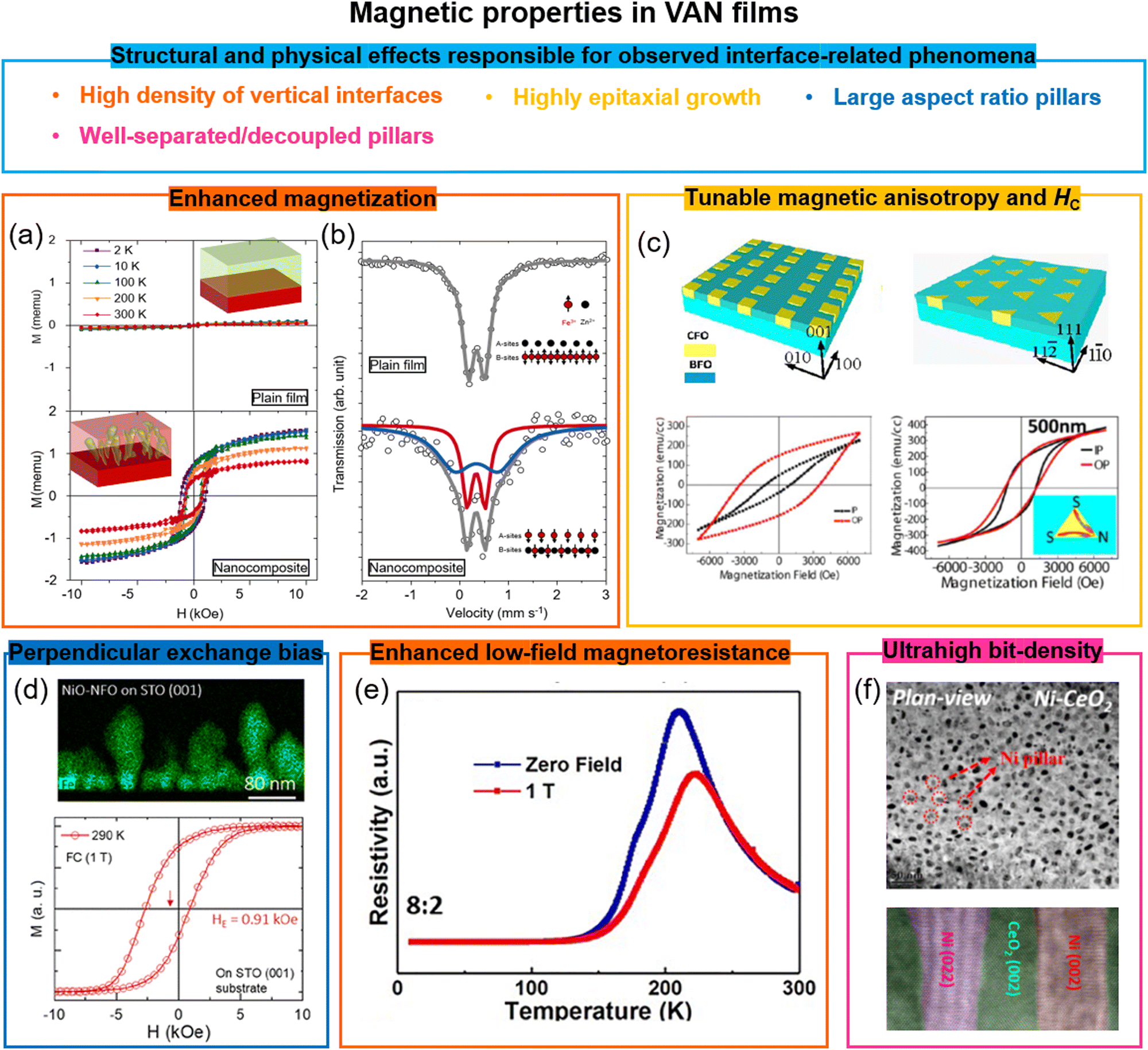 | ||
| Fig. 7 Enhanced magnetic properties achieved using VAN structures. (a) The magnetic hysteresis loops of a ZnFe2O4 plain film and a ZnFe2O4–SrTiO3 VAN film grown on a SrTiO3 (001) substrate, measured at different temperatures. The magnetic field was applied in the OOP direction. Reproduced with permission.34 Copyright 2018 Wiley-VCH. The insets show schematics of a plain ZnFe2O4 film and a ZnFe2O4–SrTiO3 VAN film, respectively. (b) Mössbauer spectra of the Fe element in the ZnFe2O4 plain film and the ZnFe2O4–SrTiO3 VAN film. The insets show schematics of the magnetic structures of the ZnFe2O4 phases. Reproduced with permission.34 Copyright 2018 Wiley-VCH. (c) Tunable magnetic anisotropy and coercivity in BiFeO3–CoFe2O4 VAN films grown on SrTiO3 substrates with magnetic field applied either in-plane (IP) or OOP. Reproduced with permission.120 Copyright 2013 American Chemical Society. (d) Enhanced perpendicular exchange bias effect in a NiO–NiFe2O4 VAN film with magnetic field applied OOP. Reproduced with permission.22 Copyright 2018 American Chemical Society. (e) Temperature dependence of the resistivity measured at different magnetic fields applied OOP. Reproduced with permission.121 Copyright 2019 AIP Publishing. (f) Plan-view (top panel) and cross-sectional (bottom panel) high resolution TEM images of a CeO2–Ni VAN film. Reproduced with permission.122 Copyright 2016 Royal Society of Chemistry. | ||
Similar antiferromagnetic-to-ferromagnetic property switching has also been also observed in other VAN films, e.g. SmMnO3–Bi2O3,96d (Sr,Sm)MnO3–Sm2O3,118 and EuTiO3–Eu2O3.119 In all cases, large vertical strains were induced, e.g. in the latter case the value was ∼3.15% in the EuTiO3 phase. The strain decreases the Eu–Ti–Eu bond angle along 〈111〉 up to 1°, leading to a weakening of the antiferromagnetic interactions and switching from antiferromagnetic to ferromagnetic behaviour.
7.2 Highly tunable magnetic anisotropy and coercivity in VAN films
The magnetic anisotropy defines the direction of the magnetization in magnetic materials. In continuous magnetic thin films, the anisotropy is usually dominated by shape anisotropy, which makes the in-plane (IP) direction the easy plane for the magnetization to minimize the demagnetization energy. However, perpendicular magnetic anisotropy (PMA) is required to achieve ultra-high-density data recording.123 In traditional media, PMA is obtained in the ultrathin films and films with noble metals or rare-earth elements with strong spin–orbit coupling, such as Co/Pt multilayers124 and DyCo5,125etc. In magnetic oxide films, PMA is typically generated using epitaxial strain-induced magnetostrictive anisotropy126 or it is driven by symmetry mismatch127 at the interfaces which leads to distinct orbital reconstructions. However, due to the interfacial nature of PMA, in standard planar films (including SL), the effect degrades with film thickness above a few nm to tens of nm depending on the mechanism for the PMA.In VAN films the total anisotropy is controlled by three kinds of magnetic anisotropy, i.e. magnetocrystalline, shape and magnetostrictive. While magnetocrystalline anisotropy is an inherent property of the material, shape and magnetostrictive anisotropy are highly tunable in VAN structures. Because of the large aspect ratio of the magnetic nanopillars which grow in VAN films, a large shape anisotropy is produced with an easy axis along the OOP direction, producing the PMA. A shape anisotropy field Hshape = 2.0 kOe was estimated in the BaTiO3–CoFe2O4 VAN films, where the aspect ratio of magnetic pillars was around 10.36 The shape anisotropy is controlled by substrate orientation (as well as other growth parameters). The substrate orientation effect on the magnetic anisotropy and coercivity has been demonstrated for CoFe2O4 pillars in BiFeO3–CoFe2O4 VAN films (Fig. 7c) as well as also for other VAN systems.120,128 Since BiFeO3 is an antiferromagnet, it has been proposed that spin-flop exchange coupling between the compensated BiFeO3 and the CoFe2O4 spins at the interfaces might contribute to the observed PMA in BiFeO3–CoFe2O4 VAN films.129
Strain-induced stress anisotropy in VAN films also plays a significant role via the magnetoelastic effect. Here, the magnetoelastic energy depends on both the magnetostriction coefficient of the magnetic material as well the strain in it. CoFe2O4 has a large magnetostrictive coefficient with a large strain-induced magnetoelastic effect. In BaTiO3–CoFe2O4 VAN films, a compressive strain in the CoFe2O4 columns of ∼0.8% is achieved, with corresponding anisotropy field of Hstress = 34 kOe, matching the coercivity of the measured magnetic hysteresis.130 The magnetostrictive and magnetocrystalline anisotropies have been systematically tuned by varying the chemical composition of the CoxNi1−xFe2O4 column phases in the CoxNi1−xFe2O4–BiFeO3 VAN system.131 Large tunability of magnetic anisotropy and coercivity has also been achieved in La0.7Sr0.3MnO3–MgO VAN, where a switch from the easy-plane magnetic anisotropy to PMA occurs as the volume ratio of MgO increases, thus leading to different strain values in the La0.7Sr0.3MnO3 matrix.60a
Potential systems for high-density perpendicular recording media have also been shown in ferromagnetic metal pillar-oxide VAN systems.132 Favourable properties such as ultra-high bit densities of ∼Tb in−2 (Fig. 7f shows an example for a CeO2–Ni film),133 uniaxial anisotropy, strong OOP magnetization, high coercivities, anisotropic electric conductivity,132b and higher TCs and lower intrinsic resistances than ferromagnetic oxides133,134 have all been demonstrated.
7.3 High perpendicular exchange bias in VAN films
Perpendicular exchange bias (PEB) is appealing for applications in perpendicular magnetic tunneling junctions (MTJs). Owing to PMA in VAN systems, PEB is also expected. Another advantage of VAN compared to traditional FM/AFM bilayers or SLs, where a HE ∼ 1/tF law (where HE and tF are the EB field and film thickness) is obeyed, is that exchange bias (EB) scales with tF, because the coupled vertical interfacial area scales with tF.The first trial PEB system was a (BiFeO3)0.9–(Fe3O4)0.1 composite film (Fe3O4 nanoparticles in a BiFeO3 film). A PEB field of HE ∼ 0.04 kOe was obtained at room temperature.112b Later, larger PEB values were obtained in LaFeO3–La0.7Sr0.3MnO3 and BiFeO3–La0.7Sr0.3MnO3 VAN systems with EB fields up to ∼1 kOe,112c,d although this was achieved at a relatively low temperatures (<10 K). Most recently, a large PEB of ∼0.91 kOe at room temperature was obtained in the NiO–NiFe2O4 VAN system (Fig. 7d).22 With the benefits of both high TC and high TN of the FM and AF materials as well as TC > TN, the blocking temperature (TB) in this system reached above 400 K.
8. Multiferroics and the magnetoelectric effect in VAN films
The key aims for non-volatile memory devices are large ME coupling coefficient at room temperature, and self-biased characteristics (electric field control of magnetism and no applied magnetic field). While, there are many reviews on both SL and VAN for creating artificial multiferroics, i.e. use of coupled systems rather than an intrinsic single phase material,135 there has been insufficient information discussing the problems of achieving ‘practical’ systems using two different materials forms and how to overcome these. We cover these points below.A strong advantage of VAN artificial multiferroics over SL are minimal clamping from the underlying substrate. Clamping prevents effective vertical strain and strain coupling of a ferroelectric with a magnetostrictive material to produce a change in magnetisation with applied voltage to give the converse magnetoelectric effect (CME), or change in polarisation with change in magnetisation to give the direct magnetoelectric effect (DME).
BaTiO3–CoFe2O4 was the first VAN film explored for achieving the ME effect.130 However, owing to poor electrical insulation of most ferromagnetic materials in multiferroic nanocomposites, only thermally-driven ME coupling was demonstrated. On the other hand, it has been shown in many different VAN systems e.g. BaTiO3–CoFe2O4,130 Ni0.5Zn0.5Fe2O4–BaTiO3136 and Y3Fe5O12–BaTiO3137 (Fig. 8a). However, thermal ME provides only indirect evidence of ME coupling, as the strain is not induced by an electric field.
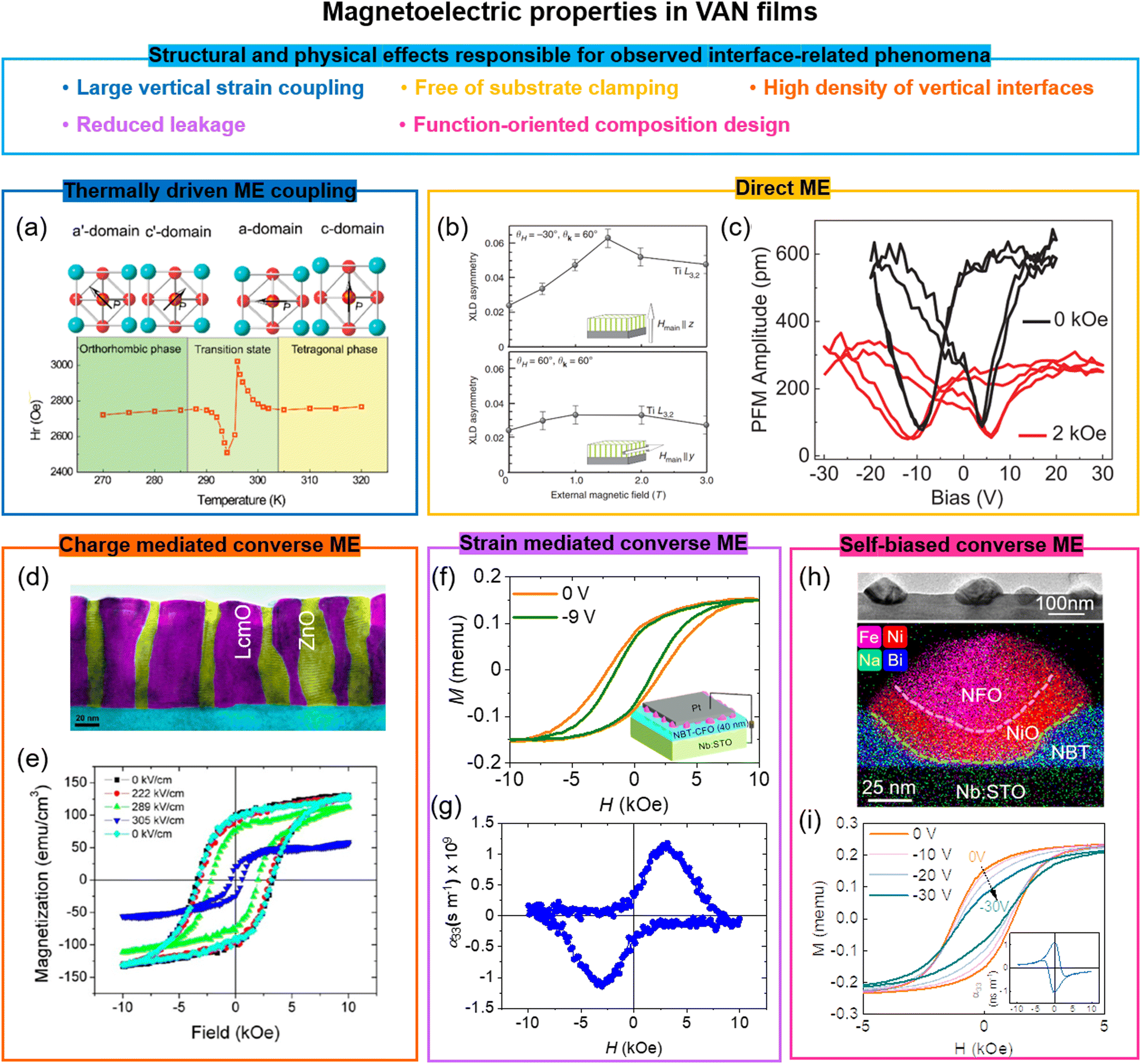 | ||
| Fig. 8 Enhanced magnetoelectric properties achieved using VAN structures. (a) Thermally-driven ME effect in Y3Fe5O12–BaTiO3 VAN films detected by the FMR. Reproduced with permission.137 Copyright 2017 American Chemical Society. (b) XLD asymmetry study of the lattice distortion induced by magnetic field in a BaTiO3–CoFe2O4 VAN film, the upper plot showing magnetic field applied OOP and the lower plot showing the magnetic field applied IP. Reproduced with permission.138a Copyright 2013 Springer Nature. (c) The effect of the application of IP magnetic field on the amplitude–voltage butterfly loop (DME effect) in BaTiO3–CoFe2O4 VAN films. Reproduced with permission.138b Copyright 2019 Wiley-VCH. (d and e) Charge mediated ME to give the CME effect in La2CoMnO6–ZnO VAN film. Reproduced with permission.142 Copyright 2013 American Chemical Society. (d) Cross-sectional (false-colour) TEM image of the La2CoMnO6–ZnO VAN film. (e) Electric field dependence of the magnetic hysteresis loops of La2CoMnO6–ZnO VAN film where the magnetic field is applied IP. (f) In situ electric field control of magnetization (CME effect) in Na0.5Bi0.5TiO3–CoFe2O4 VAN film where the magnetic field is applied OOP. Reproduced with permission.143 Copyright 2018 American Chemical Society. The inset shows a schematic of the application of an in situ electric field. (g) The magnetoelectric coefficient of the Na0.5Bi0.5TiO3–CoFe2O4 VAN film calculated from the magnetic hysteresis loops given in (f). (h) Cross-sectional TEM and EDX image of a 50 nm-thick Na0.5Bi0.5TiO3–NiO–NiFe2O4 film. Reproduced with permission.40 Copyright 2021 Springer Nature. (i) In situ electric field control of magnetization (CME effect) in a 200 nm-thick Na0.5Bi0.5TiO3–NiO–NiFe2O4 VAN film where the magnetic field is applied OOP. The inset shows the magnetoelectric coefficient, calculated from the magnetic hysteresis loops. Reproduced with permission.40 Copyright 2021 Springer Nature. | ||
In terms of DME, the BaTiO3–CoFe2O4 system is a key exemplar system.138 Here, magnetic field induced strain has been observed using different methods, X-ray linear dichroism (XLD) (Fig. 8b),138a second-harmonic generation,138b and by measuring the modified PFM amplitude upon applying a magnetic field along both IP and OOP directions (Fig. 8c).138b,139 However, possibly owing to leakage problems, a direct electric readout of DME has not been reported.
The first direct measurement of the CME effect was shown in BiFeO3–CoFe2O4 VAN.140 Here, magnetic hysteresis loops were measured to detect the change of magnetization upon applying ex situ electric field pulses. However, this system suffered leakage as revealed by conductive atomic force microscopy (c-AFM) and cross-sectional scanning tunnelling microscopy (XSTM).15a,141
In La2CoMnO6–ZnO VAN films, in situ measurements showed the existence of the CME effect as well as tunability of magnetization and coercivity (Fig. 8d and e).142 It was determined that voltage-controlled charge trapping-detrapping in the ZnO at the high-density vertical interfaces led to a modified transition metal ion valence of Mn or Co in the La2CoMnO6 and hence to a change in the magnetic state of the ferrimagnetic La2CoMnO6. However, the low TC of La2CoMnO6 (<210 K) in the thin films meant that the CME was observed only at a relatively low temperature (120 K).
The first direct measurement of a large CME effect at room temperature was observed in a VAN system of Na0.5Bi0.5TiO3–CoFe2O4. By using the wide bandgap (3.3 eV), high TC (603 K) Na0.5Bi0.5TiO3 ferroelectric instead of the commonly studied, lower TC and lower bandgap BaTiO3 and BiFeO3 ferroelectrics, a large-scale in situ electric field control of the magnetic anisotropy was obtained at room temperature (Fig. 8f).143 The relatively low leakage was linked to (a) the lower leakage ferroelectric, (b) reduction of VAN vertical interface leakage which can arise when mixed valence transition metal cations are present in the system, and most importantly (c) the formation of a rectifying interface between the film and the substrate, enabling current blockage. An CME coefficient of around 1.25 × 10⁻⁹ S m−1, at a bias field of ∼0.3 T, was achieved (Fig. 8g).
Taking the above result one step further, a function-oriented composition design approach was used to reduce leakage even more. Hence, an antiferromagnetic (AFM) phase was incorporated into a similar VAN composition as discussed above,40 making a triple composite system. Here, a triple VAN 3-1 structure of FE-AFM-FM Na0.5Bi0.5TiO3–NiO–NiFe2O4 was created (Fig. 8h). We note that AFM materials have so far played an important role in traditional spintronic devices as pinning layers,144 and as emerging AFM spintronic devices, offering ultrafast (∼THz) dynamics, high stability to external fields, and absence of stray fields.145 However, they have largely been overlooked in multiferroic VANs. In the triple VAN system, the high TC (603 K) of Na0.5Bi0.5TiO3 was again exploited, as above. But in addition, the soft magnetism of NiFe2O4, the high Néel temperature (525 K) of NiO, and the large exchange coupling between the FM and AFM material was also capitalised upon.
A large, self-biased (zero applied magnetic field) CME effect at room temperature with a ME coefficient of up to 1.38 × 10⁻⁹ s m−1 was achieved (Fig. 8i). The self-biased CME effect is ascribed to 3 critical features introduced by the addition of NiO: the leakage is strongly suppressed by the introduction of p-type NiO; the antiferromagnetic spins are rotated by the strain due to the large magnetostrictive effect of NiO, as indicated by the electric controllable EB effect; and the exchange coupling between the AFM NiO spins and the FM NiFe2O4 spins enhance the overall ME effect. This one-shot growth film, which does not rely on precise control of composition since if one phase has a slightly different ratio than another it will not be of detriment to the coupling effect, holds much promise for wide ranging applications relating to non-volatile memory and magnetic sensors.146 The next steps for this work are to demonstrate growth on TiN/Si.
C. Summary, perspectives and conclusions
9. Summary of ferroic phenomena in VAN films
VAN films formed from complex oxides provide an excellent platform for achieving enhanced ferroic properties in thin films by a one-shot process, i.e. the creating of self-assembled composite films. So far, most of the VAN systems have focused on strain coupling effects across the vertical interfaces, which give rise to 3D strain tuning of the bulk of the film, thus tuning the film properties up to micron thickness levels. The anisotropic nature of the nanopillars in VAN films can enable magnetic anisotropy effects to be tuned. VANs are different to the SL films where most emphasis has been on emergent interface properties and much thinner films. There has been much less emphasis on emergent interface effects in VAN films and there is a strong opportunity to explore more in this direction. The challenges for VAN are that there are limitations on what materials can be combined together, that the interfaces are non-ideal 2D, and that there may be more than one interface type in a given system. Overall, VAN films have strong promise for enhancing properties of ferroic films which are required to be relatively thick (e.g. actuator/energy harvesting), anisotropic (e.g. for perpendicular magnetic recording), or unclamped (e.g. multiferroic).10. Future perspectives
Throughout the paper, we highlighted the different scientific discoveries and ferroic functionalities arising in oxide superlattice (SL) and self-assembled vertically aligned nanocomposite (VAN) structures. Using exemplars, we also discussed how and why the two systems offer different and often complementary effects. Below, we highlight some underexplored/emerging research directions for ferroic properties in both oxide superlattices and VAN systems.10.1 Future perspective for superlattice films
1. Although many SL examples discussed have great potential for the discovery of new physical phenomena, one must always be aware of the many subtleties in dealing with these intrinsically nanoscale systems. As summarized in Fig. 1 and Table 1, in terms of tuning the functionalities of superlattice films, defects (cationic intermixing, point defect segregation, structural inhomogeneities, oxygen vacancies and so on) all play important, often poorly understood and interlinked roles. More work employing high intensity spectroscopic tools should be employed to understand the nature of the interface structures. Also, in order to minimise the role of interfacial strain which often produces a defective interface, focus on systems with minimal interfacial mismatch should be explored. This can be done by using new single crystal substrate compositions. There has been some excellent work in this direction in recent years.147Also, to minimise strain and defect formation, the choice of more closely lattice matched layers in the SL films should be explored, where possible. To minimise cation non-stoichiometry in films, growth under lower oxidation conditions should be studied.148 To minimise defects, films could be grown higher temperatures (i.e. at above 1000 °C rather than the conventional 700–800 °C).149 However, considering a key driver is to make oxide SLs CMOS compatible, other strategies to minimise defects at ∼500 °C and below must also be considered, e.g. atomic layer growth methods where epitaxial perovskite films have been grown at <300 °C,150 as well as novel ways to enhance growth kinetics and also carefully control composition.14
2. Most ferroic SLs have been grown mainly on perovskite substrates with (001)-orientation. Epitaxial integration of ferroic superlattices with different crystal orientation other than (001) should be explored. This field has grown rapidly in the past decade but there are many more materials combinations to be explored. Non-(001) orientations give different surface/interface terminations, neutral charge states and 2D-like structures (e.g. (111) orientations giving buckled honeycombs). Also, growth on a range of buffered semiconductor substrates beyond the well-studied Si, e.g. on Ge, Si–Ge, GaAs, GaN, and for flexible electronics, flexible substrates, e.g. mica151 or analogous crystals needs to be explored.
3. Room-temperature ferroelectricity and ferromagnetism have been widely achieved in superlattice films. However, room-temperature multiferroic superlattices with strong and robust magnetoelectric coupling have still not been realized. Since lift-off procedures for oxide films are now quite well established,86,91,152 this allows clamping effects to be overcome and so more work could be directed here to achieve robust, crack-free, non-wrinkled and well adhered films. Also, the vast majority of work on superlattices has focused on A/B superlattices. However, there is a largely unexplored area of multicomponent superlattices with complex periodicities. These could offer much further potential for achieving interesting ferroic behaviour. An example was shown for tricolor superlattices in Fig. 4, where three constituent materials forming an ABC periodicity. With the ABC periodicity, inversion symmetry is broken, enabling interesting novel magnetoelectric phenomena to be achieved.
4. There remains much to be understood about emergent phenomena, such as polar skyrmions, vortices, negative capacitance, and so on. Real-space topological textures such as polar skyrmions and vortices have been observed, but we are still in the early stages of the exploration of these phenomena. For example, the dynamics of such skyrmions structures and vortices must be explored in detail. In addition, these topologies demonstrate chirality and if this can be manipulated by an external field (such as an electric field), then this would provide a powerful way to use the chirality as an externally controllable order parameter.
5. The interfaces between 3d TMOs and 5d TMOs provide a new fruitful research area. Again, current research is still in the early stages and limited to a few systems, so more systematic investigations are highly desired to fully unravel the unique role of 5d TMOs which in turn could provide more candidates to search for novel magnetic textures and topological phenomena. Moreover, owing to the inherent mixture of spin and orbital degrees of freedom in 5d TMOs, these superlattices may open a new pathway to achieve robust electric field control of magnetism at room temperature and above.
10.2 Future perspective for VAN films
1. Just as for SL films, VAN films are subject to a range of interface and bulk point and line defects, such as mutual doping of components.153 To further optimise the perfection of these structures, similar application of spectroscopic tools, and the implementation of carefully controlled growth processes combined with a range of theoretical predictions of microstructure evolution, should take place.2. As highlighted in Table 1, the wide ranging emergent interface phenomena, topological, skyrmion and polar vortices observed in SL films have not been observed in VAN films. Considering the very high epitaxial quality of VAN films, the ultraclean self-assembled interfaces, and the ability to control dimensionalities down to a few nm via controlling growth conditions, there are unique opportunities to discover and control these novel effects in VAN.
3. Combining VAN and SLs to form 3D film architectures has not yet been widely studied.154 However, these structures could offer the chance to combine the complementary advantages of both methods and should be explored further.
4. Pulsed laser deposition is the main method to make VAN films with good quality. However, the method is area-limited. However, promising growth of a limited number of VAN systems by sputtering155 and chemical methods156 show the possibility for growth by methods of industrial interest. More work should be focused in these areas.
5. As already noted, compared to SL films, VAN films can exhibit more bulk-like effects, i.e. interface-driven effects throughout the whole film, not just right at the interfaces. Their simplicity of fabrication is also an important aspect. However, typically they have a random column distribution. For some applications, such as data storage, a highly ordered arrangement is desired. Templating by a variety of ways can produce the desired order,2b,155a,157 recently spontaneous order has been shown.2b More work is needed to determine which methods are most practical for applications.
6. Just as for SLs, mentioned above, most VAN film work has been undertaken on single crystal substrates although progress has been made with STO/TiN-buffered Si158 and with mica,159 and lifted-off films onto Si.92 More work is required on these’other substrates’ as well as new ways to grow directly on Si, e.g. using remote epitaxy.
7. As shown in Section 6, high crystalline quality mesoporous films derived from VAN films give enhanced ferroelectric effects and they also exploit high area surface effects for photocatalysis. There are many new opportunities to exploit the large surface area effects or to create new composites (not just oxide–oxide but also oxide–metal and oxide–organic systems) by chemical coating of mesoporous films made by selective chemical etching of VAN films. With this broader range of compositions, new coupling effects in wide ranging functional systems can be realised.
11. Conclusions
Over more than three decades, fascinating physical phenomena have been achieved in heteroepitaxial interfaces in complex oxide superlattices (SLs), and over the last two decades in vertically aligned nanocomposites (VANs). Numerous novels or enhanced ferroic phenomena have been achieved which have been highlighted in this review. The subtlety of the different natures of the interfaces in these two materials forms, SL or VAN, enables highly complementary phenomena to be achieved. Notably, SL films with 2D interfaces enable basic emergent physical phenomena to be discovered and explored, for example the creation of ferroelectricity,11,12,15,16 ferromagnetism,41,42,45 and multiferroism,63 emergent polar skyrmions and vortices,25,27etc. On the other hand, VAN films offer greater simplicity of growth, cleaner self-assembled interfaces, are largely unclamped by the substrate, and can be grown to micron thickness. On the other hand, they have more complex geometric vertical interfaces, and a much narrower range of materials can be grown. VAN are more suited to the engineering of ferroic properties, e.g. to increase the ferroelectric TC,21,54 to increase the magnetization34,115,119 and to enhance the magnetoelectric coupling.130,143,160 For both material forms, there are many new avenues to be explored for property discoveries and the creation of practical engineering devices, with several examples highlighted in this review, e.g. topological textures, negative capacitance, integration with silicon and other semiconductor substrates, flexibilization, etc.Conflicts of interest
There are no conflicts of interest to declare.Acknowledgements
The authors acknowledge support from Leverhulme Trust grant # RPG-2015-017, EPSRC grants EP/L011700/1, EP/N004272/1, EP/M000524/1, the Royal Academy of Engineering Chair in Emerging Technologies Grant CiET1819\24, and the ERC Advanced Grant EU-H2020-ERC-ADG #882929, EROS. R. W. also acknowledges support from the National Natural Science Foundation of China (Grant No. 12104052) and State Key Lab of Luminescent Materials and Devices, South China University of Technology (Grant No. Skllmd-2022-05). W.-W. L. also acknowledges support from the National Natural Science Foundation of China (Grant No. 52102177), the National Natural Science Foundation of Jiangsu Province (Grant No. BK20210313), Top-notch Academic Programs Project of Jiangsu Higher Education Institutions (TAPP), and the Jiangsu Specially-Appointed Professor Program.References
- (a) R. Ramesh and D. G. Schlom, Nat. Rev. Mater., 2019, 4, 257 CrossRef; (b) S. Das, A. Ghosh, M. R. McCarter, S. L. Hsu, Y. L. Tang, A. R. Damodaran, R. Ramesh and L. W. Martin, APL Mater., 2018, 6, 100901 CrossRef; (c) J. Zhang and R. D. Averitt, Annu. Rev. Mater. Res., 2014, 44, 19 CrossRef CAS; (d) P. Zubko, S. Gariglio, M. Gabay, P. Ghosez and J. M. Triscone, Annu. Rev. Condens. Matter Phys., 2011, 2, 141 CrossRef CAS; (e) D. G. Schlom, L. Q. Chen, C. B. Eom, K. M. Rabe, S. K. Streiffer and J. M. Triscone, Annu. Rev. Mater. Res., 2007, 37, 589 CrossRef CAS.
- (a) A. Chen, Q. Su, H. Han, E. Enriquez and Q. Jia, Adv. Mater., 2019, 31, e1803241 CrossRef PubMed; (b) X. Sun, J. L. MacManus-Driscoll and H. Y. Wang, Annu. Rev. Mater. Res., 2020, 50, 229 CrossRef CAS; (c) J. J. Huang, J. L. MacManus-Driscoll and H. Y. Wang, J. Mater. Res., 2017, 32, 4054 CrossRef CAS.
- M. Dawber, K. M. Rabe and J. F. Scott, Rev. Mod. Phys., 2005, 77, 1083 CrossRef CAS.
- J. X. Guo, W. W. Chen, H. S. Chen, Y. N. Zhao, F. Dong, W. W. Liu and Y. Zhang, Adv. Opt. Mater., 2021, 9, 2002146 CrossRef CAS.
- L. W. Martin and A. M. Rappe, Nat. Rev. Mater., 2016, 2, 16087 CrossRef.
- (a) H. Takasu, J. Electroceram., 2000, 4, 327 CrossRef CAS; (b) C. S. Hwang and T. Mikolajick, in Advances in Non-Volatile Memory and Storage Technology, ed. B. Magyari-Köpe and Y. Nishi, Woodhead Publishing, 2019 Search PubMed; (c) N. Setter, D. Damjanovic, L. Eng, G. Fox, S. Gevorgian, S. Hong, A. Kingon, H. Kohlstedt, N. Y. Park, G. B. Stephenson, I. Stolitchnov, A. K. Taganstev, D. V. Taylor, T. Yamada and S. Streiffer, J. Appl. Phys., 2006, 100, 051606 CrossRef; (d) G. H. Haertling, J. Am. Ceram. Soc., 1999, 82, 797 CrossRef CAS; (e) J. F. Scott, Science, 2007, 315, 954 CrossRef CAS PubMed; (f) A. Kursumovic, W. W. Li, S. Cho, P. J. Curran, D. H. L. Tjhe and J. L. MacManus-Driscoll, Nano Energy, 2020, 71, 104536 CrossRef CAS.
- G. Varvaro and F. Casoli, Ultra-High-Density Magnetic Recording: Storage Materials and Media Designs, Pan Stanford Publishing, 2016 Search PubMed.
- K. L. Wang, J. G. Alzate and P. K. Amiri, J. Phys. D: Appl. Phys., 2013, 46, 074003 CrossRef CAS.
- (a) J. F. Scott, Nat. Mater., 2007, 6, 256 CrossRef CAS PubMed; (b) M. Bibes and A. Barthelemy, Nat. Mater., 2008, 7, 425 CrossRef CAS PubMed; (c) S. H. Baek, H. W. Jang, C. M. Folkman, Y. L. Li, B. Winchester, J. X. Zhang, Q. He, Y. H. Chu, C. T. Nelson, M. S. Rzchowski, X. Q. Pan, R. Ramesh, L. Q. Chen and C. B. Eom, Nat. Mater., 2010, 9, 309 CrossRef CAS PubMed.
- Z. Chen, X. Wang, Y. Qi, S. Yang, J. A. Soares, B. A. Apgar, R. Gao, R. Xu, Y. Lee, X. Zhang, J. Yao and L. W. Martin, ACS Nano, 2016, 10, 10237 CrossRef CAS PubMed.
- R. Zhao, W. Li, J. H. Lee, E. M. Choi, Y. Liang, W. Zhang, R. Tang, H. Wang, Q. Jia, J. L. MacManus-Driscoll and H. Yang, Adv. Funct. Mater., 2014, 24, 5240 CrossRef CAS.
- J. L. MacManus-Driscoll, P. Zerrer, H. Wang, H. Yang, J. Yoon, A. Fouchet, R. Yu, M. G. Blamire and Q. Jia, Nat. Mater., 2008, 7, 314 CrossRef CAS PubMed.
- J. MacManus-Driscoll, A. Suwardi, A. Kursumovic, Z. X. Bi, C. F. Tsai, H. Y. Wang, Q. X. Jia and O. J. Lee, APL Mater., 2015, 3, 062507 CrossRef.
- J. L. MacManus-Driscoll, M. P. Wells, C. Yun, J. W. Lee, C. B. Eom and D. G. Schlom, APL Mater., 2020, 8, 040904 CrossRef CAS.
- (a) Y. H. Hsieh, J. M. Liou, B. C. Huang, C. W. Liang, Q. He, Q. Zhan, Y. P. Chiu, Y. C. Chen and Y. H. Chu, Adv. Mater., 2012, 24, 4564 CrossRef CAS PubMed; (b) B. Zhu, G. Schusteritsch, P. Lu, J. L. Macmanus-Driscoll and C. J. Pickard, APL Mater., 2019, 7, 061105 CrossRef.
- Z. Hiroi, H. Hayamizu, T. Yoshida, Y. Muraoka, Y. Okamoto, J. Yamaura and Y. Ueda, Chem. Mater., 2013, 25, 2202 CrossRef CAS.
- J. L. MacManus-Driscoll, Adv. Funct. Mater., 2010, 20, 2035 CrossRef CAS.
- (a) A. P. Chen, Z. X. Bi, Q. X. Jia, J. L. MacManus-Driscoll and H. Y. Wang, Acta Mater., 2013, 61, 2783 CrossRef CAS; (b) W. R. Zhang, A. P. Chen, Z. K. Bi, Q. X. Jia, J. L. MacManus-Driscoll and H. Y. Wang, Curr. Opin. Solid State Mater. Sci., 2014, 18, 6 CrossRef CAS.
- (a) W. R. Zhang, R. Ramesh, J. L. MacManus-Driscoll and H. Y. Wang, MRS Bull., 2015, 40, 736 CrossRef; (b) J. L. MacManus-Driscoll, A. Suwardi and H. Wang, MRS Bull., 2015, 40, 933 CrossRef CAS.
- E. M. Choi, A. Di Bernardo, B. Zhu, P. Lu, H. Alpern, K. H. L. Zhang, T. Shapira, J. Feighan, X. Sun, J. Robinson, Y. Paltiel, O. Millo, H. Wang, Q. Jia and J. L. MacManus-Driscoll, Sci. Adv., 2019, 5, eaav5532 CrossRef CAS PubMed.
- S. A. Harrington, J. Zhai, S. Denev, V. Gopalan, H. Wang, Z. Bi, S. A. Redfern, S. H. Baek, C. W. Bark, C. B. Eom, Q. Jia, M. E. Vickers and J. L. Macmanus-Driscoll, Nat. Nanotechnol., 2011, 6, 491 CrossRef CAS PubMed.
- R. Wu, C. Yun, X. Wang, P. Lu, W. Li, Y. Lin, E.-M. Choi, H. Wang and J. L. MacManus-Driscoll, ACS Appl. Mater. Interfaces, 2018, 10, 42593 CrossRef CAS PubMed.
- D. A. Tenne, A. Bruchhausen, N. D. Lanzillotti-Kimura, A. Fainstein, R. S. Katiyar, A. Cantarero, A. Soukiassian, V. Vaithyanathan, J. H. Haeni, W. Tian, D. G. Schlom, K. J. Choi, D. M. Kim, C. B. Eom, H. P. Sun, X. Q. Pan, Y. L. Li, L. Q. Chen, Q. X. Jia, S. M. Nakhmanson, K. M. Rabe and X. X. Xi, Science, 2006, 313, 1614 CrossRef CAS PubMed.
- H. N. Lee, H. M. Christen, M. F. Chisholm, C. M. Rouleau and D. H. Lowndes, Nature, 2005, 433, 395 CrossRef CAS PubMed.
- O. Lee, A. Kursumovic, Z. Bi, C. F. Tsai, H. Wang and J. L. MacManus-Driscoll, Adv. Mater. Interfaces, 2017, 4, 1700336 CrossRef.
- N. M. Dawley, E. J. Marksz, A. M. Hagerstrom, G. H. Olsen, M. E. Holtz, V. Goian, C. Kadlec, J. Zhang, X. Lu, J. A. Drisko, R. Uecker, S. Ganschow, C. J. Long, J. C. Booth, S. Kamba, C. J. Fennie, D. A. Muller, N. D. Orloff and D. G. Schlom, Nat. Mater., 2020, 19, 176 CrossRef CAS PubMed.
- O. Lee, S. A. Harrington, A. Kursumovic, E. Defay, H. Wang, Z. Bi, C. F. Tsai, L. Yan, Q. Jia and J. L. MacManus-Driscoll, Nano Lett., 2012, 12, 4311 CrossRef CAS PubMed.
- (a) W. Gao, A. Khan, X. Marti, C. Nelson, C. Serrao, J. Ravichandran, R. Ramesh and S. Salahuddin, Nano Lett., 2014, 14, 5814 CrossRef CAS PubMed; (b) S. Das, Y. L. Tang, Z. Hong, M. A. P. Goncalves, M. R. McCarter, C. Klewe, K. X. Nguyen, F. Gomez-Ortiz, P. Shafer, E. Arenholz, V. A. Stoica, S. L. Hsu, B. Wang, C. Ophus, J. F. Liu, C. T. Nelson, S. Saremi, B. Prasad, A. B. Mei, D. G. Schlom, J. Iniguez, P. Garcia-Fernandez, D. A. Muller, L. Q. Chen, J. Junquera, L. W. Martin and R. Ramesh, Nature, 2019, 568, 368 CrossRef CAS PubMed.
- (a) A. K. Yadav, C. T. Nelson, S. L. Hsu, Z. Hong, J. D. Clarkson, C. M. Schleputz, A. R. Damodaran, P. Shafer, E. Arenholz, L. R. Dedon, D. Chen, A. Vishwanath, A. M. Minor, L. Q. Chen, J. F. Scott, L. W. Martin and R. Ramesh, Nature, 2016, 530, 198 CrossRef CAS PubMed; (b) P. Shafer, P. Garcia-Fernandez, P. Aguado-Puente, A. R. Damodaran, A. K. Yadav, C. T. Nelson, S. L. Hsu, J. C. Wojdel, J. Iniguez, L. W. Martin, E. Arenholz, J. Junquera and R. Ramesh, Proc. Natl. Acad. Sci. U. S. A., 2018, 115, 915 CrossRef CAS PubMed.
- C. He, A. J. Grutter, M. Gu, N. D. Browning, Y. Takamura, B. J. Kirby, J. A. Borchers, J. W. Kim, M. R. Fitzsimmons, X. Zhai, V. V. Mehta, F. J. Wong and Y. Suzuki, Phys. Rev. Lett., 2012, 109, 197202 CrossRef CAS PubMed.
- B. Negulescu, L. Thomas, Y. Dumont, M. Tessier, N. Keller and M. Guyot, J. Magn. Magn. Mater., 2002, 242–245, 529 CrossRef CAS.
- (a) K. Ueda, H. Tabata and T. Kawai, Science, 1998, 280, 1064 CrossRef CAS PubMed; (b) K. Ueda, H. Tabata and T. Kawai, J. Appl. Phys., 2001, 89, 2847 CrossRef CAS.
- E. Weal, S. Patnaik, Z. Bi, H. Wang, T. Fix, A. Kursumovic and J. L. M. Driscoll, Appl. Phys. Lett., 2010, 97, 153121 CrossRef.
- C. Park, R. Wu, P. Lu, H. Zhao, J. B. Yang, B. Zhang, W. W. Li, C. Yun, H. Y. Wang, J. L. MacManus-Driscoll and S. Cho, Adv. Funct. Mater., 2018, 28, 1706220 CrossRef.
- D. Yi, C. L. Flint, P. P. Balakrishnan, K. Mahalingam, B. Urwin, A. Vailionis, A. T. N'Diaye, P. Shafer, E. Arenholz, Y. Choi, K. H. Stone, J. H. Chu, B. M. Howe, J. Liu, I. R. Fisher and Y. Suzuki, Phys. Rev. Lett., 2017, 119, 077201 CrossRef PubMed.
- H. M. Zheng, J. Kreisel, Y. H. Chu, R. Ramesh and L. Salamanca-Riba, Appl. Phys. Lett., 2007, 90, 113113 CrossRef.
- E. Skoropata, J. Nichols, J. M. Ok, R. V. Chopdekar, E. S. Choi, A. Rastogi, C. Sohn, X. Gao, S. Yoon, T. Farmer, R. D. Desautels, Y. Choi, D. Haskel, J. W. Freeland, S. Okamoto, M. Brahlek and H. N. Lee, Sci. Adv., 2020, 6, eaaz3902 CrossRef CAS PubMed.
- (a) M. Lorenz, G. Wagner, V. Lazenka, P. Schwinkendorf, H. Modarresi, M. J. Van Bael, A. Vantomme, K. Temst, O. Oeckler and M. Grundmann, Appl. Phys. Lett., 2015, 106, 012905 CrossRef; (b) M. Lorenz, D. Hirsch, C. Patzig, T. Hoche, S. Hohenberger, H. Hochmuth, V. Lazenka, K. Temst and M. Grundmann, ACS Appl. Mater. Interfaces, 2017, 9, 18956 CrossRef CAS PubMed.
- L. Yan, Z. P. Xing, Z. G. Wang, T. Wang, G. Y. Lei, J. F. Li and D. Viehland, Appl. Phys. Lett., 2009, 94 Search PubMed.
- R. Wu, D. Zhang, T. Maity, P. Lu, J. Yang, X. Gao, S. Zhao, X. Wei, H. Zeng, A. Kursumovic, G. Tian, W. Li, C. Yun, Y. Wang, Z. Ren, Z. Zhou, M. Liu, K. H. L. Zhang, Q. Jia, J. Yang, H. Wang and J. L. MacManus-Driscoll, Nat. Electron., 2021, 4, 333 CrossRef CAS.
- K. Rogdakis, J. W. Seo, Z. Viskadourakis, Y. Wang, L. F. Qune, E. Choi, J. D. Burton, E. Y. Tsymbal, J. Lee and C. Panagopoulos, Nat. Commun., 2012, 3, 1064 CrossRef CAS PubMed.
- V. A. Stoica, N. Laanait, C. Dai, Z. Hong, Y. Yuan, Z. Zhang, S. Lei, M. R. McCarter, A. Yadav, A. R. Damodaran, S. Das, G. A. Stone, J. Karapetrova, D. A. Walko, X. Zhang, L. W. Martin, R. Ramesh, L. Q. Chen, H. Wen, V. Gopalan and J. W. Freeland, Nat. Mater., 2019, 18, 377 CrossRef CAS PubMed.
- R. Mishra, Y. M. Kim, J. Salafranca, S. K. Kim, S. H. Chang, A. Bhattacharya, D. D. Fong, S. J. Pennycook, S. T. Pantelides and A. Y. Borisevich, Nano Lett., 2014, 14, 2694 CrossRef CAS PubMed.
- S. Cho, C. Yun, S. Tappertzhofen, A. Kursumovic, S. Lee, P. Lu, Q. Jia, M. Fan, J. Jian, H. Wang, S. Hofmann and J. L. MacManus-Driscoll, Nat. Commun., 2016, 7, 12373 CrossRef CAS PubMed.
- J. M. Rondinelli and C. J. Fennie, Adv. Mater., 2012, 24, 1961 CrossRef CAS PubMed.
- H. Zhang, Y. Weng, X. Yao and S. Dong, Phys. Rev. B: Condens. Matter Mater. Phys., 2015, 91, 195145 CrossRef.
- S. Y. Park, A. Kumar and K. M. Rabe, Phys. Rev. Lett., 2017, 118, 087602 CrossRef PubMed.
- S. Ghosh, A. Y. Borisevich and S. T. Pantelides, Phys. Rev. Lett., 2017, 119, 177603 CrossRef PubMed.
- (a) J. Ravichandran, A. K. Yadav, R. Cheaito, P. B. Rossen, A. Soukiassian, S. J. Suresha, J. C. Duda, B. M. Foley, C. H. Lee, Y. Zhu, A. W. Lichtenberger, J. E. Moore, D. A. Muller, D. G. Schlom, P. E. Hopkins, A. Majumdar, R. Ramesh and M. A. Zurbuchen, Nat. Mater., 2014, 13, 168 CrossRef CAS PubMed; (b) W. Tian, J. C. Jiang, X. Q. Pan, J. H. Haeni, Y. L. Li, L. Q. Chen, D. G. Schlom, J. B. Neaton, K. M. Rabe and Q. X. Jia, Appl. Phys. Lett., 2006, 89, 092905 CrossRef.
- (a) S. S. A. Seo, J. H. Lee, H. N. Lee, M. F. Chisholm, W. S. Choi, D. J. Kim, J. Y. Jo, H. Kim, J. Yu and T. W. Noh, Adv. Mater., 2007, 19, 2460 CrossRef CAS; (b) X. Wu, K. M. Rabe and D. Vanderbilt, Phys. Rev. B: Condens. Matter Mater. Phys., 2011, 83, 020104 CrossRef.
- (a) S. Berber, Y. K. Kwon and D. Tomanek, Phys. Rev. Lett., 2000, 84, 4613 CrossRef CAS PubMed; (b) X. Wu, M. Stengel, K. M. Rabe and D. Vanderbilt, Phys. Rev. Lett., 2008, 101, 087601 CrossRef PubMed.
- (a) C. C. Homes, T. Vogt, S. M. Shapiro, S. Wakimoto and A. P. Ramirez, Science, 2001, 293, 673 CrossRef CAS PubMed; (b) S. Krohns, P. Lunkenheimer, S. Meissner, A. Reller, B. Gleich, A. Rathgeber, T. Gaugler, H. U. Buhl, D. C. Sinclair and A. Loidl, Nat. Mater., 2011, 10, 899 CrossRef CAS PubMed.
- (a) A. K. Tagantsev, V. O. Sherman, K. F. Astafiev, J. Venkatesh and N. Setter, J. Electroceram., 2003, 11, 5 CrossRef CAS; (b) P. Bao, T. J. Jackson, X. Wang and M. J. Lancaster, J. Phys. D: Appl. Phys., 2008, 41, 063001 CrossRef.
- A. L. Sangle, O. J. Lee, A. Kursumovic, W. Zhang, A. Chen, H. Wang and J. L. MacManus-Driscoll, Nanoscale, 2018, 10, 3460 RSC.
- E. Bousquet, M. Dawber, N. Stucki, C. Lichtensteiger, P. Hermet, S. Gariglio, J. M. Triscone and P. Ghosez, Nature, 2008, 452, 732 CrossRef CAS PubMed.
- W. Zhong and D. Vanderbilt, Phys. Rev. Lett., 1995, 74, 2587 CrossRef CAS PubMed.
- X. Gao, D. Zhang, X. Wang, J. Jian, Z. He, H. Dou and H. Wang, Nanoscale Adv., 2020, 2, 3276 RSC.
- (a) A. K. Yadav, K. X. Nguyen, Z. Hong, P. Garcia-Fernandez, P. Aguado-Puente, C. T. Nelson, S. Das, B. Prasad, D. Kwon, S. Cheema, A. I. Khan, C. Hu, J. Iniguez, J. Junquera, L. Q. Chen, D. A. Muller, R. Ramesh and S. Salahuddin, Nature, 2019, 565, 468 CrossRef CAS PubMed; (b) S. Salahuddin and S. Datta, Nano Lett., 2008, 8, 405 CrossRef CAS PubMed; (c) P. Zubko, J. C. Wojdel, M. Hadjimichael, S. Fernandez-Pena, A. Sene, I. Luk'yanchuk, J. M. Triscone and J. Iniguez, Nature, 2016, 534, 524 CrossRef CAS PubMed; (d) J. Íñiguez, P. Zubko, I. Luk’yanchuk and A. Cano, Nat. Rev. Mater., 2019, 4, 243 CrossRef.
- I. Kornev, H. Fu and L. Bellaiche, Phys. Rev. Lett., 2004, 93, 196104 CrossRef PubMed.
- (a) A. Chen, J. M. Hu, P. Lu, T. Yang, W. Zhang, L. Li, T. Ahmed, E. Enriquez, M. Weigand, Q. Su, H. Wang, J. X. Zhu, J. L. MacManus-Driscoll, L. Q. Chen, D. Yarotski and Q. Jia, Sci. Adv., 2016, 2, e1600245 CrossRef PubMed; (b) R. Zhao, C. Yang, H. Wang, K. Jiang, H. Wu, S. Shen, L. Wang, Y. Sun, K. Jin, J. Gao, L. Chen, H. Wang, J. L. MacManus-Driscoll, P. A. van Aken, J. Hong, W. Li and H. Yang, Nat. Commun., 2022, 13, 2364 CrossRef CAS PubMed.
- (a) M. B. Salamon and M. Jaime, Rev. Mod. Phys., 2001, 73, 583 CrossRef CAS; (b) J. M. Rondinelli and N. A. Spaldin, Adv. Mater., 2011, 23, 3363 CrossRef CAS PubMed; (c) W. Li, B. Zhu, Q. He, A. Y. Borisevich, C. Yun, R. Wu, P. Lu, Z. Qi, Q. Wang, A. Chen, H. Wang, S. A. Cavill, K. H. L. Zhang and J. L. MacManus-Driscoll, Adv. Sci., 2020, 7, 1901606 CrossRef CAS PubMed.
- M. Gibert, P. Zubko, R. Scherwitzl, J. Iniguez and J. M. Triscone, Nat. Mater., 2012, 11, 195 CrossRef CAS PubMed.
- A. Bhattacharya and S. J. May, Annu. Rev. Mater. Res., 2014, 44, 65 CrossRef CAS.
- W. W. Li, B. N. Zhu, R. X. Zhu, Q. Wang, P. Lu, Y. W. Sun, C. Cafolla, Z. M. Qi, A. P. Chen, P. Gao, H. Y. Wang, Q. He, K. H. L. Zhang and J. L. MacManus-Driscoll, Adv. Funct. Mater., 2020, 30, 2001984 CrossRef CAS.
- D. Yi, J. Liu, S. L. Hsu, L. Zhang, Y. Choi, J. W. Kim, Z. Chen, J. D. Clarkson, C. R. Serrao, E. Arenholz, P. J. Ryan, H. Xu, R. J. Birgeneau and R. Ramesh, Proc. Natl. Acad. Sci. U. S. A., 2016, 113, 6397 CrossRef CAS PubMed.
- H. Y. Hwang, Y. Iwasa, M. Kawasaki, B. Keimer, N. Nagaosa and Y. Tokura, Nat. Mater., 2012, 11, 103 CrossRef CAS PubMed.
- K. S. Takahashi, M. Kawasaki and Y. Tokura, Appl. Phys. Lett., 2001, 79, 1324 CrossRef CAS.
- S. Dong and E. Dagotto, Phys. Rev. B: Condens. Matter Mater. Phys., 2013, 87, 195116 CrossRef.
- I. Loa, P. Adler, A. Grzechnik, K. Syassen, U. Schwarz, M. Hanfland, G. K. Rozenberg, P. Gorodetsky and M. P. Pasternak, Phys. Rev. Lett., 2001, 87, 125501 CrossRef CAS PubMed.
- A. Bhattacharya, S. J. May, S. G. te Velthuis, M. Warusawithana, X. Zhai, B. Jiang, J. M. Zuo, M. R. Fitzsimmons, S. D. Bader and J. N. Eckstein, Phys. Rev. Lett., 2008, 100, 257203 CrossRef CAS PubMed.
- C. Aruta, C. Adamo, A. Galdi, P. Orgiani, V. Bisogni, N. B. Brookes, J. C. Cezar, P. Thakur, C. A. Perroni, G. De Filippis, V. Cataudella, D. G. Schlom, L. Maritato and G. Ghiringhelli, Phys. Rev. B: Condens. Matter Mater. Phys., 2009, 80, 140405 CrossRef.
- (a) H. Yang, H. Wang, J. Yoon, Y. Wang, M. Jain, D. M. Feldmann, P. C. Dowden, J. L. MacManus-Driscoll and Q. Jia, Adv. Mater., 2009, 21, 3794 CrossRef CAS; (b) Y. H. Hsieh, E. Strelcov, J. M. Liou, C. Y. Shen, Y. C. Chen, S. V. Kalinin and Y. H. Chu, ACS Nano, 2013, 7, 8627 CrossRef CAS PubMed.
- (a) S. Lee, A. Sangle, P. Lu, A. Chen, W. Zhang, J. S. Lee, H. Wang, Q. Jia and J. L. MacManus-Driscoll, Adv. Mater., 2014, 26, 6284 CrossRef CAS PubMed; (b) S. Lee and J. L. MacManus-Driscoll, APL Mater., 2017, 5, 042304 CrossRef.
- K. Ueda, H. Tabata and T. Kawai, J. Appl. Phys., 2001, 89, 2847 CrossRef CAS.
- A. Sadoc, B. Mercey, C. Simon, D. Grebille, W. Prellier and M. B. Lepetit, Phys. Rev. Lett., 2010, 104, 046804 CrossRef PubMed.
- (a) L. Qiao, J. H. Jang, D. J. Singh, Z. Gai, H. Xiao, A. Mehta, R. K. Vasudevan, A. Tselev, Z. Feng, H. Zhou, S. Li, W. Prellier, X. Zu, Z. Liu, A. Borisevich, A. P. Baddorf and M. D. Biegalski, Nano Lett., 2015, 15, 4677 CrossRef CAS PubMed; (b) J. M. Rondinelli, S. J. May and J. W. Freeland, MRS Bull., 2012, 37, 261 CrossRef CAS.
- X. Zhai, L. Cheng, Y. Liu, C. M. Schleputz, S. Dong, H. Li, X. Zhang, S. Chu, L. Zheng, J. Zhang, A. Zhao, H. Hong, A. Bhattacharya, J. N. Eckstein and C. Zeng, Nat. Commun., 2014, 5, 4283 CrossRef CAS PubMed.
- S. Okamoto, J. Nichols, C. Sohn, S. Y. Kim, T. W. Noh and H. N. Lee, Nano Lett., 2017, 17, 2126 CrossRef CAS PubMed.
- J. Nichols, X. Gao, S. Lee, T. L. Meyer, J. W. Freeland, V. Lauter, D. Yi, J. Liu, D. Haskel, J. R. Petrie, E.-J. Guo, A. Herklotz, D. Lee, T. Z. Ward, G. Eres, M. R. Fitzsimmons and H. N. Lee, Nat. Commun., 2016, 7, 12721 CrossRef CAS PubMed.
- M. A. Marioni, M. Penedo, M. Bacani, J. Schwenk and H. J. Hug, Nano Lett., 2018, 18, 2263 CrossRef CAS PubMed.
- N. A. Hill, J. Phys. Chem. B, 2000, 104, 6694 CrossRef CAS.
- X. He and K. J. Jin, Phys. Rev. B: Condens. Matter Mater. Phys., 2016, 93, 161108 CrossRef.
- H. Guo, Z. Wang, S. Dong, S. Ghosh, M. Saghayezhian, L. Chen, Y. Weng, A. Herklotz, T. Z. Ward, R. Jin, S. T. Pantelides, Y. Zhu, J. Zhang and E. W. Plummer, Proc. Natl. Acad. Sci. U. S. A., 2017, 114, E5062 CAS.
- Y. Tokura, J. Magn. Magn. Mater., 2007, 310, 1145 CrossRef CAS.
- J. A. Mundy, C. M. Brooks, M. E. Holtz, J. A. Moyer, H. Das, A. F. Rebola, J. T. Heron, J. D. Clarkson, S. M. Disseler, Z. Liu, A. Farhan, R. Held, R. Hovden, E. Padgett, Q. Mao, H. Paik, R. Misra, L. F. Kourkoutis, E. Arenholz, A. Scholl, J. A. Borchers, W. D. Ratcliff, R. Ramesh, C. J. Fennie, P. Schiffer, D. A. Muller and D. G. Schlom, Nature, 2016, 537, 523 CrossRef CAS PubMed.
- D. Ji, S. Cai, T. R. Paudel, H. Sun, C. Zhang, L. Han, Y. Wei, Y. Zang, M. Gu, Y. Zhang, W. Gao, H. Huyan, W. Guo, D. Wu, Z. Gu, E. Y. Tsymbal, P. Wang, Y. Nie and X. Pan, Nature, 2019, 570, 87 CrossRef CAS PubMed.
- (a) S. Singh, J. T. Haraldsen, J. Xiong, E. M. Choi, P. Lu, D. Yi, X. D. Wen, J. Liu, H. Wang, Z. Bi, P. Yu, M. R. Fitzsimmons, J. L. MacManus-Driscoll, R. Ramesh, A. V. Balatsky, J. X. Zhu and Q. X. Jia, Phys. Rev. Lett., 2014, 113, 047204 CrossRef PubMed; (b) E. J. Guo, J. R. Petrie, M. A. Roldan, Q. Li, R. D. Desautels, T. Charlton, A. Herklotz, J. Nichols, J. van Lierop, J. W. Freeland, S. V. Kalinin, H. N. Lee and M. R. Fitzsimmons, Adv. Mater., 2017, 29, 1700790 CrossRef PubMed.
- (a) Y. Ogawa, H. Yamada, T. Ogasawara, T. Arima, H. Okamoto, M. Kawasaki and Y. Tokura, Phys. Rev. Lett., 2003, 90, 217403 CrossRef CAS PubMed; (b) N. Kida, H. Yamada, H. Sato, T. Arima, M. Kawasaki, H. Akoh and Y. Tokura, Phys. Rev. Lett., 2007, 99, 197404 CrossRef CAS PubMed.
- H. Das, A. L. Wysocki, Y. Geng, W. Wu and C. J. Fennie, Nat. Commun., 2014, 5, 2998 CrossRef PubMed.
- (a) A. T. Chen, H. L. Huang, Y. Wen, W. Y. Liu, S. F. Zhang, J. Kosel, W. D. Sun, Y. G. Zhao, Y. L. Lu and X. X. Zhang, Mater. Horiz., 2020, 7, 2328 RSC; (b) M. Chen, M. G. Ju, H. F. Garces, A. D. Carl, L. K. Ono, Z. Hawash, Y. Zhang, T. Shen, Y. Qi, R. L. Grimm, D. Pacifici, X. C. Zeng, Y. Zhou and N. P. Padture, Nat. Commun., 2019, 10, 16 CrossRef CAS PubMed; (c) E. Lage, C. Kirchhof, V. Hrkac, L. Kienle, R. Jahns, R. Knochel, E. Quandt and D. Meyners, Nat. Mater., 2012, 11, 523 CrossRef CAS PubMed.
- G. Dong, S. Li, M. Yao, Z. Zhou, Y. Q. Zhang, X. Han, Z. Luo, J. Yao, B. Peng, Z. Hu, H. Huang, T. Jia, J. Li, W. Ren, Z. G. Ye, X. Ding, J. Sun, C. W. Nan, L. Q. Chen, J. Li and M. Liu, Science, 2019, 366, 475 CrossRef CAS PubMed.
- B. Zhang, C. Yun and J. L. MacManus-Driscoll, Nanomicro Lett., 2021, 13, 39 Search PubMed.
- (a) J. H. Haeni, P. Irvin, W. Chang, R. Uecker, P. Reiche, Y. L. Li, S. Choudhury, W. Tian, M. E. Hawley, B. Craigo, A. K. Tagantsev, X. Q. Pan, S. K. Streiffer, L. Q. Chen, S. W. Kirchoefer, J. Levy and D. G. Schlom, Nature, 2004, 430, 758 CrossRef CAS PubMed; (b) K. J. Choi, M. Biegalski, Y. L. Li, A. Sharan, J. Schubert, R. Uecker, P. Reiche, Y. B. Chen, X. Q. Pan, V. Gopalan, L. Q. Chen, D. G. Schlom and C. B. Eom, Science, 2004, 306, 1005 CrossRef CAS PubMed; (c) L. Zhang, J. Chen, L. Fan, O. Dieguez, J. Cao, Z. Pan, Y. Wang, J. Wang, M. Kim, S. Deng, J. Wang, H. Wang, J. Deng, R. Yu, J. F. Scott and X. Xing, Science, 2018, 361, 494 CrossRef CAS PubMed.
- (a) S. C. Wimbush, M. C. Li, M. E. Vickers, B. Maiorov, D. M. Feldmann, Q. X. Jia and J. L. MacManus-Driscoll, Adv. Funct. Mater., 2009, 19, 835 CrossRef CAS; (b) V. Nagarajan, C. L. Jia, H. Kohlstedt, R. Waser, I. B. Misirlioglu, S. P. Alpay and R. Ramesh, Appl. Phys. Lett., 2005, 86, 192910 CrossRef; (c) F. Sandiumenge, J. Santiso, L. Balcells, Z. Konstantinovic, J. Roqueta, A. Pomar, J. P. Espinos and B. Martinez, Phys. Rev. Lett., 2013, 110, 107206 CrossRef PubMed.
- C. Yun, E.-M. Choi, W. Li, X. Sun, T. Maity, R. Wu, J. Jian, S. Xue, S. Cho and H. Wang, Nanoscale, 2020, 12, 9255 RSC.
- (a) H. Yang, H. Wang, G. F. Zou, M. Jain, N. A. Suvorova, D. M. Feldmann, P. C. Dowden, R. F. DePaula, J. L. MacManus-Driscoll, A. J. Taylor and Q. X. Jia, Appl. Phys. Lett., 2008, 93, 142904 CrossRef; (b) Y. H. Hsieh, F. Xue, T. Yang, H. J. Liu, Y. Zhu, Y. C. Chen, Q. Zhan, C. G. Duan, L. Q. Chen, Q. He and Y. H. Chu, Nat. Commun., 2016, 7, 13199 CrossRef CAS PubMed; (c) X. Zhang, R. Xu, X. Gao, Y. Ji, F. Qian, J. Fan, H. Wang, W. Li and H. Yang, J. Mater. Chem. C, 2020, 8, 8091 RSC; (d) E. M. Choi, T. Maity, A. Kursumoyic, P. Lu, Z. H. Bi, S. K. Yu, Y. Park, B. N. Zhu, R. Wu, V. Gopalan, H. Y. Wang and J. L. MacManus-Driscoll, Nat. Commun., 2020, 11, 2207 CrossRef CAS PubMed.
- H. Liu, H. Wu, K. P. Ong, T. Yang, P. Yang, P. K. Das, X. Chi, Y. Zhang, C. Diao, W. K. A. Wong, E. P. Chew, Y. F. Chen, C. K. I. Tan, A. Rusydi, M. B. H. Breese, D. J. Singh, L. Q. Chen, S. J. Pennycook and K. Yao, Science, 2020, 369, 292 CrossRef CAS PubMed.
- K.-i Sakayori, Y. Matsui, H. Abe, E. Nakamura, M. Kenmoku, T. Hara, D. Ishikawa, A. Kokubu, K.-i Hirota and T. Ikeda, Jpn. J. Appl. Phys., 1995, 34, 5443 CrossRef CAS.
- D. A. Tenne, A. Bruchhausen, N. D. Lanzillotti-Kimura, A. Fainstein, R. S. Katiyar, A. Cantarero, A. Soukiassian, V. Vaithyanathan, J. H. Haeni, W. Tian, D. G. Schlom, K. J. Choi, D. M. Kim, C. B. Eom, H. P. Sun, X. Q. Pan, Y. L. Li, L. Q. Chen, Q. X. Jia, S. M. Nakhmanson, K. M. Rabe and X. X. Xi, Science, 2006, 313, 1614 CrossRef CAS PubMed.
- (a) F. Khatkhatay, A. Chen, J. H. Lee, W. Zhang, H. Abdel-Raziq and H. Wang, ACS Appl. Mater. Interfaces, 2013, 5, 12541 CrossRef CAS PubMed; (b) X. Y. Zhang, R. X. Xu, X. Y. Gao, M. Li, X. N. Shi, Y. D. Ji, F. J. Qian, J. Y. Fan, H. Y. Wang, W. W. Li and H. Yang, Appl. Surf. Sci., 2020, 516, 146093 CrossRef CAS; (c) W. Li, R. Zhao, R. Tang, A. Chen, W. Zhang, X. Lu, H. Wang and H. Yang, ACS Appl. Mater. Interfaces, 2014, 6, 5356 CrossRef CAS PubMed; (d) W. Li, W. Zhang, L. Wang, J. Gu, A. Chen, R. Zhao, Y. Liang, H. Guo, R. Tang, C. Wang, K. Jin, H. Wang and H. Yang, Sci. Rep., 2015, 5, 11335 CrossRef PubMed.
- M. C. Rose and R. E. Cohen, Phys. Rev. Lett., 2012, 109, 187604 CrossRef PubMed.
- C. A. Randall, A. Kelnberger, G. Y. Yang, R. E. Eitel and T. R. Shrout, J. Electroceram., 2005, 14, 177 CrossRef.
- M. J. Chen, X. K. Ning, S. F. Wang and G. S. Fu, RSC Adv., 2017, 7, 38231 RSC.
- D. Zhang, D. Sando, P. Sharma, X. Cheng, F. Ji, V. Govinden, M. Weyland, V. Nagarajan and J. Seidel, Nat. Commun., 2020, 11, 349 CrossRef CAS PubMed.
- P. C. Joshi and S. B. Krupanidhi, Appl. Phys. Lett., 1993, 62, 1928 CrossRef CAS.
- S. V. Kiselev, R. P. Ozerov and G. S. Zhdanov, Sov. Phys. Dokl, 1963, 7, 742 Search PubMed.
- Y. N. Venevtsev, G. Zhadanow and S. Solov’ev, Sov. Phys. Crystallogr., 1960, 4, 538 Search PubMed.
- (a) A. Tsurumaki, H. Yamada and A. Sawa, Adv. Funct. Mater., 2012, 22, 1040 CrossRef CAS; (b) A. Q. Jiang, C. Wang, K. J. Jin, X. B. Liu, J. F. Scott, C. S. Hwang, T. A. Tang, H. B. Lu and G. Z. Yang, Adv. Mater., 2011, 23, 1277 CrossRef CAS PubMed.
- R. U. Chandrasena, W. Yang, Q. Lei, M. U. Delgado-Jaime, K. D. Wijesekara, M. Golalikhani, B. A. Davidson, E. Arenholz, K. Kobayashi, M. Kobata, F. M. de Groot, U. Aschauer, N. A. Spaldin, X. Xi and A. X. Gray, Nano Lett., 2017, 17, 794 CrossRef CAS PubMed.
- A. L. Sangle, S. Singh, J. Jian, S. R. Bajpe, H. Wang, N. Khare and J. L. MacManus-Driscoll, Nano Lett., 2016, 16, 7338 CrossRef CAS PubMed.
- S. Singh, A. L. Sangle, T. Wu, N. Khare and J. L. MacManus-Driscoll, ACS Appl. Mater. Interfaces, 2019, 11, 45683 CrossRef CAS PubMed.
- (a) S.-H. Kim, H. Choi, K. No and S.-C. Shin, J. Phys. D: Appl. Phys., 2010, 43 CAS; (b) E. M. Choi, E. Weal, Z. X. Bi, H. Y. Wang, A. Kursumovic, T. Fix, M. G. Blamire and J. L. MacManus-Driscoll, Appl. Phys. Lett., 2013, 102, 012905 CrossRef; (c) W. Zhang, A. Chen, J. Jian, Y. Zhu, L. Chen, P. Lu, Q. Jia, J. L. MacManus-Driscoll, X. Zhang and H. Wang, Nanoscale, 2015, 7, 13808 RSC; (d) M. Fan, W. R. Zhang, J. Jian, J. J. Huang and H. Y. Wang, APL Mater., 2016, 4, 076105 CrossRef.
- R. L. Stamps, S. Breitkreutz, J. Akerman, A. V. Chumak, Y. Otani, G. E. W. Bauer, J. U. Thiele, M. Bowen, S. A. Majetich, M. Klaui, I. L. Prejbeanu, B. Dieny, N. M. Dempsey and B. Hillebrands, J. Phys. D: Appl. Phys., 2014, 47, 333001 CrossRef.
- S. Sun, C. B. Murray, D. Weller, L. Folks and A. Moser, Science, 2000, 287, 1989 CrossRef CAS PubMed.
- L. Shen, C. Ma, S. Cheng, S. Ren, S. Cheng, S. Mi and M. Liu, J. Mater. Chem. C, 2016, 4, 10955 RSC.
- A. Vailionis, H. Boschker, W. Siemons, E. P. Houwman, D. H. A. Blank, G. Rijnders and G. Koster, Phys. Rev. B: Condens. Matter Mater. Phys., 2011, 83, 064101 CrossRef.
- (a) C. N. Chinnasamy, A. Narayanasamy, N. Ponpandian, K. Chattopadhyay, H. Guerault and J. M. Greneche, J. Phys.: Condens. Matter, 2000, 12, 7795 CrossRef CAS; (b) F. S. Li, L. Wang, J. B. Wang, Q. G. Zhou, X. Z. Zhou, H. P. Kunkel and G. Williams, J. Magn. Magn. Mater., 2004, 268, 332 CrossRef CAS; (c) J. T. Wu, N. Li, J. Xu, Y. Q. Jiang, Z. G. Ye, Z. X. Xie and L. S. Zheng, Appl. Phys. Lett., 2011, 99, 202505 CrossRef.
- A. Suwardi, B. Prasad, S. Lee, E. M. Choi, P. Lu, W. Zhang, L. Li, M. Blamire, Q. Jia, H. Wang, K. Yao and J. L. MacManus-Driscoll, Nanoscale, 2016, 8, 8083 RSC.
- Y. Lin, E.-M. Choi, P. Lu, X. Sun, R. Wu, C. Yun, B. Zhu, H. Wang, W. Li, T. Maity and J. MacManus-Driscoll, ACS Appl. Mater. Interfaces, 2020, 12, 8513 CrossRef CAS PubMed.
- Z. Wang, Y. Li, R. Viswan, B. Hu, V. G. Harris, J. Li and D. Viehland, ACS Nano, 2013, 7, 3447 CrossRef CAS PubMed.
- X. Y. Gao, L. G. Li, J. Jian, J. J. Huang, X. Sun, D. Zhang and H. Y. Wang, Appl. Phys. Lett., 2019, 115, 053103 CrossRef.
- J. Huang, Z. Qi, L. Li, H. Wang, S. Xue, B. Zhang, X. Zhang and H. Wang, Nanoscale, 2018, 10, 17182 RSC.
- B. Dieny and M. Chshiev, Rev. Mod. Phys., 2017, 89, 025008 CrossRef.
- (a) S. Maat, K. Takano, S. S. Parkin and E. E. Fullerton, Phys. Rev. Lett., 2001, 87, 087202 CrossRef CAS PubMed; (b) P. Borisov, A. Hochstrat, X. Chen, W. Kleemann and C. Binek, Phys. Rev. Lett., 2005, 94, 117203 CrossRef PubMed.
- F. Radu, R. Abrudan, I. Radu, D. Schmitz and H. Zabel, Nat. Commun., 2012, 3, 715 CrossRef CAS PubMed.
- (a) R. Galceran, L. López-Mir, B. Bozzo, J. Cisneros-Fernández, J. Santiso, L. Balcells, C. Frontera and B. Martínez, Phys. Rev. B: Condens. Matter Mater. Phys., 2016, 93, 144417 CrossRef; (b) J. B. Fu, M. X. Hua, X. Wen, M. Z. Xue, S. L. Ding, M. Wang, P. Yu, S. Q. Liu, J. Z. Han, C. S. Wang, H. L. Du, Y. C. Yang and J. B. Yang, Appl. Phys. Lett., 2017, 110, 202403 CrossRef.
- J. Zhang, Z. Zhong, X. Guan, X. Shen, J. Zhang, F. Han, H. Zhang, H. Zhang, X. Yan, Q. Zhang, L. Gu, F. Hu, R. Yu, B. Shen and J. Sun, Nat. Commun., 2018, 9, 1923 CrossRef PubMed.
- (a) S. C. Liao, P. Y. Tsai, C. W. Liang, H. J. Liu, J. C. Yang, S. J. Lin, C. H. Lai and Y. H. Chu, ACS Nano, 2011, 5, 4118 CrossRef CAS PubMed; (b) H. Zheng, Q. Zhan, F. Zavaliche, M. Sherburne, F. Straub, M. P. Cruz, L. Q. Chen, U. Dahmen and R. Ramesh, Nano Lett., 2006, 6, 1401 CrossRef CAS PubMed; (c) O. J. Lee, S. Misra, H. Wang and J. L. MacManus-Driscoll, APL Mater., 2021, 9, 030904 CrossRef CAS.
- W. Zhang, J. Jian, A. Chen, L. Jiao, F. Khatkhatay, L. Li, F. Chu, Q. Jia, J. L. MacManus-Driscoll and H. Wang, Appl. Phys. Lett., 2014, 104, 062402 CrossRef.
- H. Zheng, J. Wang, S. E. Lofland, Z. Ma, L. Mohaddes-Ardabili, T. Zhao, L. Salamanca-Riba, S. R. Shinde, S. B. Ogale, F. Bai, D. Viehland, Y. Jia, D. G. Schlom, M. Wuttig, A. Roytburd and R. Ramesh, Science, 2004, 303, 661 CrossRef CAS PubMed.
- S. Ojha, W. C. Nunes, N. M. Aimon and C. A. Ross, ACS Nano, 2016, 10, 7657 CrossRef CAS PubMed.
- (a) L. Mohaddes-Ardabili, H. Zheng, S. B. Ogale, B. Hannoyer, W. Tian, J. Wang, S. E. Lofland, S. R. Shinde, T. Zhao, Y. Jia, L. Salamanca-Riba, D. G. Schlom, M. Wuttig and R. Ramesh, Nat. Mater., 2004, 3, 533 CrossRef CAS PubMed; (b) J. Huang, L. Li, P. Lu, Z. Qi, X. Sun, X. Zhang and H. Wang, Nanoscale, 2017, 9, 7970 RSC.
- J. Huang, Z. Qi, L. Li, H. Wang, S. Xue, B. Zhang, X. Zhang and H. Wang, Nanoscale, 2018, 10, 17182 RSC.
- Q. Su, W. Zhang, P. Lu, S. Fang, F. Khatkhatay, J. Jian, L. Li, F. Chen, X. Zhang, J. L. MacManus-Driscoll, A. Chen, Q. Jia and H. Wang, ACS Appl. Mater. Interfaces, 2016, 8, 20283 CrossRef CAS PubMed.
- (a) C. A. Vaz, J. Hoffman, C. H. Ahn and R. Ramesh, Adv. Mater., 2010, 22, 2900 CrossRef CAS PubMed; (b) J. Ma, J. Hu, Z. Li and C. W. Nan, Adv. Mater., 2011, 23, 1062 CrossRef CAS PubMed; (c) Y. Wang, J. M. Hu, Y. H. Lin and C. W. Nan, NPG Asia Mater., 2010, 2, 61 CrossRef; (d) R. Ramesh and S. Manipatruni, Proc. R. Soc. A, 2021, 477, 20200942 CrossRef.
- G. Dong, Z. Zhou, M. Guan, X. Xue, M. Chen, J. Ma, Z. Hu, W. Ren, Z. G. Ye, C. W. Nan and M. Liu, ACS Nano, 2018, 12, 3751 CrossRef CAS PubMed.
- G. Dong, Z. Zhou, X. Xue, Y. Zhang, B. Peng, M. Guan, S. Zhao, Z. Hu, W. Ren, Z. G. Ye and M. Liu, ACS Appl. Mater. Interfaces, 2017, 9, 30733 CrossRef CAS PubMed.
- (a) C. Schmitz-Antoniak, D. Schmitz, P. Borisov, F. M. de Groot, S. Stienen, A. Warland, B. Krumme, R. Feyerherm, E. Dudzik, W. Kleemann and H. Wende, Nat. Commun., 2013, 4, 2051 CrossRef PubMed; (b) A. Chen, Y. Dai, A. Eshghinejad, Z. Liu, Z. Wang, J. Bowlan, E. Knall, L. Civale, J. L. MacManus-Driscoll, A. J. Taylor, R. P. Prasankumar, T. Lookman, J. Li, D. Yarotski and Q. Jia, Adv. Sci., 2019, 6, 1901000 CrossRef CAS PubMed.
- Z. H. Mo, G. Tian, W. D. Yang, S. Ning, C. A. Ross, X. S. Gao and J. M. Liu, APL Mater., 2021, 9, 041109 CrossRef CAS.
- F. Zavaliche, H. Zheng, L. Mohaddes-Ardabili, S. Y. Yang, Q. Zhan, P. Shafer, E. Reilly, R. Chopdekar, Y. Jia, P. Wright, D. G. Schlom, Y. Suzuki and R. Ramesh, Nano Lett., 2005, 5, 1793 CrossRef CAS PubMed.
- E. Strelcov, A. Belianinov, Y. H. Hsieh, Y. H. Chu and S. V. Kalinin, Nano Lett., 2015, 15, 6650 CrossRef CAS PubMed.
- T. Fix, E. M. Choi, J. W. Robinson, S. B. Lee, A. Chen, B. Prasad, H. Wang, M. G. Blamire and J. L. Macmanus-Driscoll, Nano Lett., 2013, 13, 5886 CrossRef CAS PubMed.
- R. Wu, A. Kursumovic, X. Gao, C. Yun, M. E. Vickers, H. Wang, S. Cho and J. L. MacManus-Driscoll, ACS Appl. Mater. Interfaces, 2018, 10, 18237 CrossRef CAS PubMed.
- I. K. S. J. Nogue, J. Magn. Magn. Mater., 2002, 192, 203 CrossRef.
- T. Jungwirth, J. Sinova, A. Manchon, X. Marti, J. Wunderlich and C. Felser, Nat. Phys., 2018, 14, 200 Search PubMed.
- R. Wu and J. L. MacManus-Driscoll, APL Mater., 2022, 10 Search PubMed.
- (a) R. Uecker, R. Bertram, M. Brutzam, Z. Galazka, T. M. Gesing, C. Guguschev, D. Klimm, M. Klupsch, A. Kwasniewski and D. G. Schlom, J. Cryst. Growth, 2017, 457, 137 CrossRef CAS; (b) C. Guguschev, D. Klimm, M. Brützam, T. M. Gesing, M. Gogolin, H. Paik, T. Markurt, D. J. Kok, A. Kwasniewski, U. Jendritzki and D. G. Schlom, J. Cryst. Growth, 2020, 536, 125526 CrossRef CAS.
- J. H. Song, T. Susaki and H. Y. Hwang, Adv. Mater., 2008, 20, 2528 CrossRef CAS.
- M. Lippmaa, N. Nakagawa, M. Kawasaki, S. Ohashi and H. Koinuma, J. Electroceram., 2000, 4, 365 CrossRef CAS.
- H. H. Sonsteby, E. Skaar, O. S. Fjellvag, J. E. Bratvold, H. Fjellvag and O. Nilsen, Nat. Commun., 2020, 11, 2872 CrossRef PubMed.
- (a) J. Huang, H. Wang, X. Wang, X. Gao, J. Liu and H. Wang, ACS Appl. Mater. Interfaces, 2020, 12, 39920 CrossRef CAS PubMed; (b) T. Amrillah, Y. Bitla, K. Shin, T. Yang, Y. H. Hsieh, Y. Y. Chiou, H. J. Liu, T. H. Do, D. Su, Y. C. Chen, S. U. Jen, L. Q. Chen, K. H. Kim, J. Y. Juang and Y. H. Chu, ACS Nano, 2017, 11, 6122 CrossRef CAS PubMed.
- (a) B. Peng, R. C. Peng, Y. Q. Zhang, G. Dong, Z. Zhou, Y. Zhou, T. Li, Z. Liu, Z. Luo, S. Wang, Y. Xia, R. Qiu, X. Cheng, F. Xue, Z. Hu, W. Ren, Z. G. Ye, L. Q. Chen, Z. Shan, T. Min and M. Liu, Sci. Adv., 2020, 6, eaba5847 CrossRef CAS PubMed; (b) D. Pesquera, E. Khestanova, M. Ghidini, S. Zhang, A. P. Rooney, F. Maccherozzi, P. Riego, S. Farokhipoor, J. Kim, X. Moya, M. E. Vickers, N. A. Stelmashenko, S. J. Haigh, S. S. Dhesi and N. D. Mathur, Nat. Commun., 2020, 11, 3190 CrossRef CAS PubMed.
- (a) H.-J. Liu, V.-T. Tra, Y.-J. Chen, R. Huang, C.-G. Duan, Y.-H. Hsieh, H.-J. Lin, J.-Y. Lin, C.-T. Chen, Y. Ikuhara and Y.-H. Chu, Adv. Mater., 2013, 25, 4753 CrossRef CAS PubMed; (b) W. I. Liang, Y. Liu, S. C. Liao, W. C. Wang, H. J. Liu, H. J. Lin, C. T. Chen, C. H. Lai, A. Borisevich, E. Arenholz, J. Li and Y. H. Chu, J. Mater. Chem. C, 2014, 2, 811 RSC.
- (a) A. P. Chen, Z. Harrell, P. Lu, E. Enriquez, L. G. Li, B. Zhang, P. Dowden, C. L. Chen, H. Y. Wang, J. L. MacManus-Driscoll and Q. X. Jia, Adv. Funct. Mater., 2019, 29 CAS; (b) Y. Li, Z. Wang, J. Yao, T. Yang, Z. Wang, J. M. Hu, C. Chen, R. Sun, Z. Tian, J. Li, L. Q. Chen and D. Viehland, Nat. Commun., 2015, 6, 6680 CrossRef CAS PubMed.
- (a) T. C. Kim, S. Ojha, G. Tian, S. H. Lee, H. K. Jung, J. W. Choi, L. Kornblum, F. J. Walker, C. H. Ahn, C. A. Ross and D. H. Kim, J. Mater. Chem. C, 2018, 6, 5552 RSC; (b) T. C. Kim, S. H. Lee, H. K. Jung, Y. E. Kim, J. W. Choi, D. Yang and D. H. Kim, J. Magn. Magn. Mater., 2019, 471, 116 CrossRef CAS; (c) S. H. Lee, G. Tian, T. C. Kim, H. K. Jung, J. W. Choi, F. J. Walker, C. H. Ahn, C. A. Ross and D. H. Kim, Nanotechnology, 2019, 30, 105601 CrossRef PubMed; (d) D. H. Kim, S. Ning and C. A. Ross, J. Mater. Chem. C, 2019, 7, 9128 RSC; (e) T. C. Kim, S. H. Lee, H. K. Jung, H. Lee, J. H. Mun, I. Oh and D. H. Kim, Ceram. Int., 2019, 45, 12182 CrossRef CAS.
- (a) H. Luo, H. Yang, S. A. Baily, O. Ugurlu, M. Jain, M. E. Hawley, T. M. McCleskey, A. K. Burrell, E. Bauer, L. Civale, T. G. Holesinger and Q. Jia, J. Am. Chem. Soc., 2007, 129, 14132 CrossRef CAS PubMed; (b) S. M. Baber, Q. L. Lin, G. F. Zou, N. Haberkorn, S. A. Baily, H. Y. Wang, Z. X. Bi, H. Yang, S. G. Deng, M. E. Hawley, L. Civale, E. Bauer, T. M. McCleskey, A. K. Burrell, Q. X. Jia and H. M. Luo, J. Phys. Chem. C, 2011, 115, 25338 CrossRef CAS; (c) M. Saito, M. Hagiwara and S. Fujihara, Mater. Chem. Phys., 2019, 236, 121762 CrossRef CAS.
- (a) R. Comes, H. Liu, M. Khokhlov, R. Kasica, J. Lu and S. A. Wolf, Nano Lett., 2012, 12, 2367 CrossRef CAS PubMed; (b) S. M. Stratulat, X. Lu, A. Morelli, D. Hesse, W. Erfurth and M. Alexe, Nano Lett., 2013, 13, 3884 CrossRef CAS PubMed; (c) N. M. Aimon, H. K. Choi, X. Y. Sun, D. H. Kim and C. A. Ross, Adv. Mater., 2014, 26, 3063 CrossRef CAS PubMed; (d) M. Faustini, Nat. Mater., 2021, 20, 8 CrossRef CAS PubMed.
- W. Zhang, A. Chen, F. Khatkhatay, C. F. Tsai, Q. Su, L. Jiao, X. Zhang and H. Wang, ACS Appl. Mater. Interfaces, 2013, 5, 3995 CrossRef CAS PubMed.
- J. C. Liu, X. J. Wang, X. Y. Gao, H. Wang, J. Jian, J. J. Huang, X. Sun, Z. M. Qi, S. Misra, Z. H. He and H. Y. Wang, Appl. Mater. Today, 2020, 21, 100856 CrossRef.
- N. M. Aimon, D. H. Kim, X. Sun and C. A. Ross, ACS Appl. Mater. Interfaces, 2015, 7, 2263 CrossRef CAS PubMed.
| This journal is © The Royal Society of Chemistry 2023 |