
 Open Access Article
 This Open Access Article is licensed under a Creative Commons Attribution-Non Commercial 3.0 Unported Licence
Angle-independent solar radiation capture by 3D printed lattice structures for efficient photoelectrochemical water splitting†
Chidanand
Hegde
ab,
Tamar
Rosental
c,
Joel Ming Rui
Tan
ab,
Shlomo
Magdassi
 *bc and
Lydia Helena
Wong
*ab
*bc and
Lydia Helena
Wong
*ab
aDepartment of Materials Science and Engineering, Nanyang Technological University, Singapore, 639798, Singapore. E-mail: LydiaWong@ntu.edu.sg
bSingapore-HUJ Alliance for Research and Enterprise (SHARE), Campus for Research Excellence and Technological Enterprise (CREATE), Singapore 138602, Singapore
cCasali Center for Applied Chemistry, Institute of Chemistry, Center for Nanoscience and Nanotechnology, The Hebrew University of Jerusalem, Jerusalem, Israel. E-mail: magdassi@mail.huji.ac.il
First published on 21st February 2023
Abstract
Photoelectrochemical water splitting is one of the sustainable routes to renewable hydrogen production. One of the challenges to deploying photoelectrochemical (PEC) based electrolyzers is the difficulty in the effective capture of solar radiation as the illumination angle changes throughout the day. Herein, we demonstrate a method for the angle-independent capture of solar irradiation by using transparent 3 dimensional (3D) lattice structures as the photoanode in PEC water splitting. The transparent 3D lattice structures were fabricated by 3D printing a silica sol–gel followed by aging and sintering. These transparent 3D lattice structures were coated with a conductive indium tin oxide (ITO) thin film and a Mo-doped BiVO4 photoanode thin film by dip coating. The sheet resistance of the conductive lattice structures can reach as low as 340 Ohms per sq for ∼82% optical transmission. The 3D lattice structures furnished large volumetric current densities of 1.39 mA cm−3 which is about 2.4 times higher than a flat glass substrate (0.58 mA cm−3) at 1.23 V and 1.5 G illumination. Further, the 3D lattice structures showed no significant loss in performance due to a change in the angle of illumination, whereas the performance of the flat glass substrate was significantly affected. This work opens a new paradigm for more effective capture of solar radiation that will increase the solar to energy conversion efficiency.
New conceptsThe efficient capture of solar radiation via photoelectrochemical water splitting poses unique challenges. Developing an electrode system that can harvest solar energy at all angles of illumination and within a small space is desired to realize real-world applications. In this communication, we present a novel approach to angle-independent and efficient solar energy absorption by using transparent 3D-printed glass lattice structures as a substrate for PEC water oxidation. The transparent 3D lattice structures were prepared by 3D printing of a UV curable sol–gel silica ink, followed by sintering of the aged samples. Subsequently, the 3D lattice structures were dip-coated with conductive ITO and Mo–BiVO4 in consequent steps to construct semi-transparent 3D lattice electrodes (3DP/ITO/Mo–BiVO4). Owing to the 3D lattice design that furnishes a large surface area, the photocurrent produced by the 3DP/ITO/Mo–BiVO4 lattice structure electrodes is nearly 2.4 times higher than that of flatbed electrodes of the same volume. Moreover, the 3DP/ITO/Mo–BiVO4 lattice structure electrodes are minimally affected (within 6% deviation) by the changing angles of solar illumination making them efficient at capturing solar radiation. In summary, our design and fabrication strategy of 3D lattice electrodes opens up a new paradigm for electrode designs for photo electrocatalysis. |
Introduction
The world needs to rapidly transition to renewable energy sources to avoid the catastrophic consequences of climate change. While batteries play a crucial role as energy carriers, various sectors such as heavy transportation, shipping, and flying need more energy dense carriers.1 Amongst energy dense carriers, hydrogen is one of the cleanest2 energy carriers, since it can be sourced from water electrolysis and the product of hydrogen consumption as a fuel is also water. Therefore, sustainable and renewable hydrogen production is critical in this energy transition. Producing hydrogen through photo-electrocatalysis is one of the viable ways to produce hydrogen through the direct capture of the Sun's energy. Photo-electrocatalysis does not need additional solar panels and can also be operated without an external voltage bias as a standalone system for small-scale hydrogen production.There has been continuous advancement in the field of photo-electrocatalysis in the last few decades. Much of the work focuses on tuning the band gap of these semiconductor photo-anodes/cathodes to align with the energetics of the water splitting reaction.3–8 Some of the works also focus on the stability of these semiconductors9,10 and on finding a suitable catalyst that can enhance the functioning of these photoanodes/cathodes.11–13 These approaches are primarily driven by the search for novel materials. However, the practical deployment of PEC electrolyzers comes with unique challenges. Firstly, PEC hydrogen production requires the effective capture of solar radiation by the electrodes throughout the day. But, due to the Sun's movement, the angle of illumination of the electrode changes throughout the day, which reduces the total absorption of the incident radiation.14,15 Continuous tilting of electrodes towards the Sun's direction (similar to rotating solar panels) throughout the day16 is not viable due to the increased energy consumption and the complexity of the mechanical design. Another approach of using multiple layers of electrodes requires the transparency of the photoelectrode to facilitate solar harvesting efficiently. However, due to the coating of conductive oxides such as ITO/FTO and the subsequent coating of the photoanode/cathode the transparency is slightly reduced. Thus, the electrodes at the front end get most of the solar radiation, while the successive electrode surfaces can only absorb a fraction of the transmitted light. Therefore, there is a need to change the design of PEC electrodes for effective solar energy absorption.
Here, we attempt to address the issue of solar absorption by a new design of transparent 3D lattice electrodes. Owing to the 3D lattice structure design, the surface area of the electrode in contact with water and exposed to solar radiation is much higher than that of a series of flat glass electrodes. A higher surface area per unit volume17 gives rise to a large number of active sites and hence a higher photocurrent. In addition, owing to the pores in the lattice structures, even the lattice segments on the inner facets of the lattice are exposed to higher radiation intensities. Furthermore, the 3D lattice design provides more isotropic exposure18 of the electrode surface in all directions, due to which solar radiation is more effectively absorbed at all angles of illumination.
Despite the prospect of a 3D lattice electrode for PEC, there have been no reports on this to our knowledge. This is primarily because there is a lack of transparent lattice structures which can furnish a large surface area for depositing photoanodes/cathodes. The use of metal foams like Ni, Cu, Fe or stainless-steel foams is not suitable for photo-electrocatalysis since this application requires a highly transparent substrate for coating the photoanode/cathode to allow the incident light to access the inner layers. Furthermore, the substrate is subjected to high-temperature annealing during the coating of the thin films of the photoanodes/cathodes and conductive oxides like FTO/ITO. Thus, there is a need for transparent porous/cellular structures which are resistant to high temperatures. Unfortunately, transparent plastics do not satisfy this criterion, hence they cannot be used for such applications. On the other hand, while glass and transparent ceramics are highly suitable for this purpose, the fabrication of complex cellular structures of glass or ceramics is difficult by using conventional glass manufacturing processes. This can be overcome by utilizing 3D printing processes. In this regard, there has been good progress in 3D printing of glass and ceramic materials19–23 in recent years which opens up this new possibility. 3D printing technology enables the fabrication of complex foam/lattice structures24–26 of various degrees of porosity which is impossible with conventional methods of manufacturing. Since the manufacturing is predominantly additive, there is little to no wastage of raw materials. The 3D printing of metals, ceramics and plastics has advanced rapidly in the last decade, and only recently has there been significant progress in the 3D printing of transparent glass. Melt 3D printing of glass is one of the easiest approaches, which, however, suffers from a lack of transparency due to a lack of interlayer adhesion. Our group21,27 and others28,29 have reported the 3D printing of glass from a sol–gel precursor which resolves this issue and creates transparent 3D printed glass parts of complex shapes. Excited by this breakthrough, herein we demonstrate the potential use of transparent 3D printed glass in a new application, for photoelectrochemical water splitting.
In this work, the 3D glass lattice structures were 3D printed by the digital light processing (DLP) of printing compositions containing a photopolymerizable silica sol–gel precursor, followed by aging and sintering under a controlled atmosphere. The developed 3D printed parts were dip-coated with indium tin oxide (ITO) and Mo-doped BiVO4 to be used as a photoanode for photoelectrochemical water oxidation. The in-depth fabrication and characterization of the 3D lattice electrodes will be discussed in the following sections.
Experimental section
Chemicals
Indium (III) chloride (InCl3, Sigma Aldrich), tin chloride (SnCl2, Sigma Aldrich), bismuth (III) nitrate pentahydrate (Bi(NO3)3·5H2O), vanadyl acetyl acetonate (VO(acac)2, Sigma Aldrich), molybdenum chloride (MoCl5, Sigma Aldrich), Tetraethyl orthosilicate (TEOS, Sigma Aldrich), (3-acryloxypropyl) trimethoxysilane (APTMS, 96%, Gelest), sulforhodamine – B (Sigma Aldrich), diphenyl(2,4,6-trimethylbenzoyl)phosphine oxide (Sigma Aldrich), ammonium acetate (Sigma Aldrich), nitric acid (HNO3, VWR), hydroquinone (99%, Sigma Aldrich), and absolute ethanol (VWR) were used without further treatment.Sol–gel formulation for glass 3D printing
37.65 g of TEOS was mixed with 3.15 g of APTMS and mixed with a hydrolysis solution. The hydrolysis solution consists of 7.64 g of absolute ethanol, 2.95 g of deionized water, and 1.18 g of 1 wt% solution of HNO3. The mixture was stirred in a round bottom flask for 1 hour. After 1 hour, to the above mixture, a condensation solution comprising 65% ethanol in DI water (24.46 g) and TPO (1.118 g), and ammonium acetate (0.37 g) was mixed dropwise and stirring continued for another 45 minutes. Finally, 0.04 g of hydroquinone and 0.15 g of sulforhodamine – B were added and the mixture was chilled in an ice bath for 5 minutes. The resulting mixed was immediately transferred to the printing bath for 3D printing.3D printing
An Asiga MAX 27, digital light processing (DLP) 3D printer was used to 3D print the sol–gel. The following printing parameters were used: layer height – 200 μm, exposure time – 9 seconds, and power – 29 mW. After printing, the samples were transferred to a plastic cup and were dried at 50 °C inside an oven for 4 days. The aged samples were later sintered in a tube furnace. Initially, de-binding was conducted at 800 °C followed by sintering at 1100 °C. The details of the sintering profile are reported in our previous report.21Dip-coating of ITO and Mo-doped BiVO4
A 0.4 M solution of InCl3 and SnCl2 in isopropyl alcohol (IPA) was used for coating ITO on the 3D printed glass. The Sn concentration was fixed at 10 molar% relative to indium, which is similar to commercial ITO.30 The glass substrates were lowered into the solution and were withdrawn at a constant speed of 1 mm s−1 using a dip coater. The coated samples were dried with a blow drier and were immediately placed in the tube furnace to sinter at 600 °C for 5 minutes. During this short sintering time the In and Sn salts decompose to form thin films of ITO. The samples were removed from the furnace, cooled down and again dip coated. This cycle of dip coating, drying and sintering was repeated 5 times to give a uniform coating of ITO and finally, the coated samples were sintered at 600 °C for 2 hours. For coating Mo-doped BiVO4, a 0.03 M solution of Bi(NO3)3·5H2O and VO(acac)2 in the solvent mixture of N,N-dimethyl formamide (DMF), ethanol, and acetic acid in a 1.25![[thin space (1/6-em)]](https://www.rsc.org/images/entities/char_2009.gif) :2:1 ratio respectively was used. MoCl5 was added to the above solution to adjust the Mo doping concentration to 2% as reported in our previous work.31 The dip coating was performed according to the same procedure as for the ITO, except that the sintering temperature was fixed at 450 °C.
:2:1 ratio respectively was used. MoCl5 was added to the above solution to adjust the Mo doping concentration to 2% as reported in our previous work.31 The dip coating was performed according to the same procedure as for the ITO, except that the sintering temperature was fixed at 450 °C.
Sample characterization
The phase of the synthesized samples was determined using a Bruker – D8 XRD with Cu-Kα radiation (λ = 1.5406 Å) operated at 40 kV and 30 mA. The morphology of the samples was imaged using a JEOL field emission scanning electron microscope (JSM-7600F, JEOL Ltd Tokyo, Japan). A UV-Vis spectrophotometer was used to measure the absorption characteristics of the coated glass.Electrochemical characterization
The electrochemical measurements were done using CHI 660D work station (CH Instruments Inc.) along with a 150W Xenon solar simulator (67005, Newport Corp.). The intensity of light was adjusted to AM 1.5G (100 mW cm−2). The photoelectrochemical (PEC) oxygen evolution reaction (OER) performance was tested using a typical 3 electrode system with Ag/AgCl as the reference electrode and Pt mesh as the counter electrode, and 0.1 M KH2PO4/K2HPO4 buffer (pH = 7) as the electrolyte. The PEC OER performance was measured by linear sweep voltammetry (LSV) from 0.4 V to 1.4 V vs. Ag/AgCl at 5 mV per second. The measured potential was converted to potential vs. reversible hydrogen electrode (RHE) by using the relation Evs.RHE = Evs.Ag/AgCl + 0.0591 × pH. The estimation of the electrochemical active surface area (ECSA) was done by conducting cyclic voltammetry tests between 0.75 V and 0.85 V vs. a Ag/AgCl electrode at different scan rates viz. 10, 20, 40, 60, 80, and 100 mV s−1. The slope of the plot of capacitive current (at 0.8 V vs. Ag/AgCl) vs. the scan rates equals twice the double layer capacitance of the electrode which is a good estimate of the ECSA of the electrodes. The faradaic efficiency of the electrode during PEC testing was measured by estimating the evolved oxygen through gas chromatography (GC) and comparing it with the estimated oxygen release from the chronoamperometry curves. The gas was taken collected from the airtight electrolytic cell using a 0.5 ml syringe and injected into a GC cell for estimation of the evolved oxygen. The PEC electrolysis was paused for 2 minutes during each collection of gas which was done at every 15 minute interval.Results and discussion
A schematic of the fabrication procedure of the 3D lattice electrode is presented in Fig. 1. In the first step, 3D printing of the silica sol–gel composition was performed based on our previous report.21 Simple cubic lattice structures of 21 mm edge length were printed with various degrees of porosity. The 3D printed sol–gel was aged in a convection oven at 50 °C for 4 days to slowly evaporate the solvents from the 3DP lattice. This was followed by de-binding (800 °C) and sintering (1100 °C) to form transparent silica lattice structures as shown in Fig. 1a. The final transparent glass lattice had dimensions of around a 9 mm cube, owing to shrinkage during ageing, de-binding and sintering. For the sake of the nomenclature of the lattices with different porosity, we refer to them as 2 × 2, 3 × 3, 4 × 4, 5 × 5, and 6 × 6 lattices in this report. It is worth noting that the outer dimension of all the lattices is a 9 mm cube (Fig. 1c). Herein, 2 × 2 refers to a simple cubic lattice composed of an array of 2 × 2 holes on each face of the cube. The dimensions of the holes are twice the dimensions of the beam in all the samples.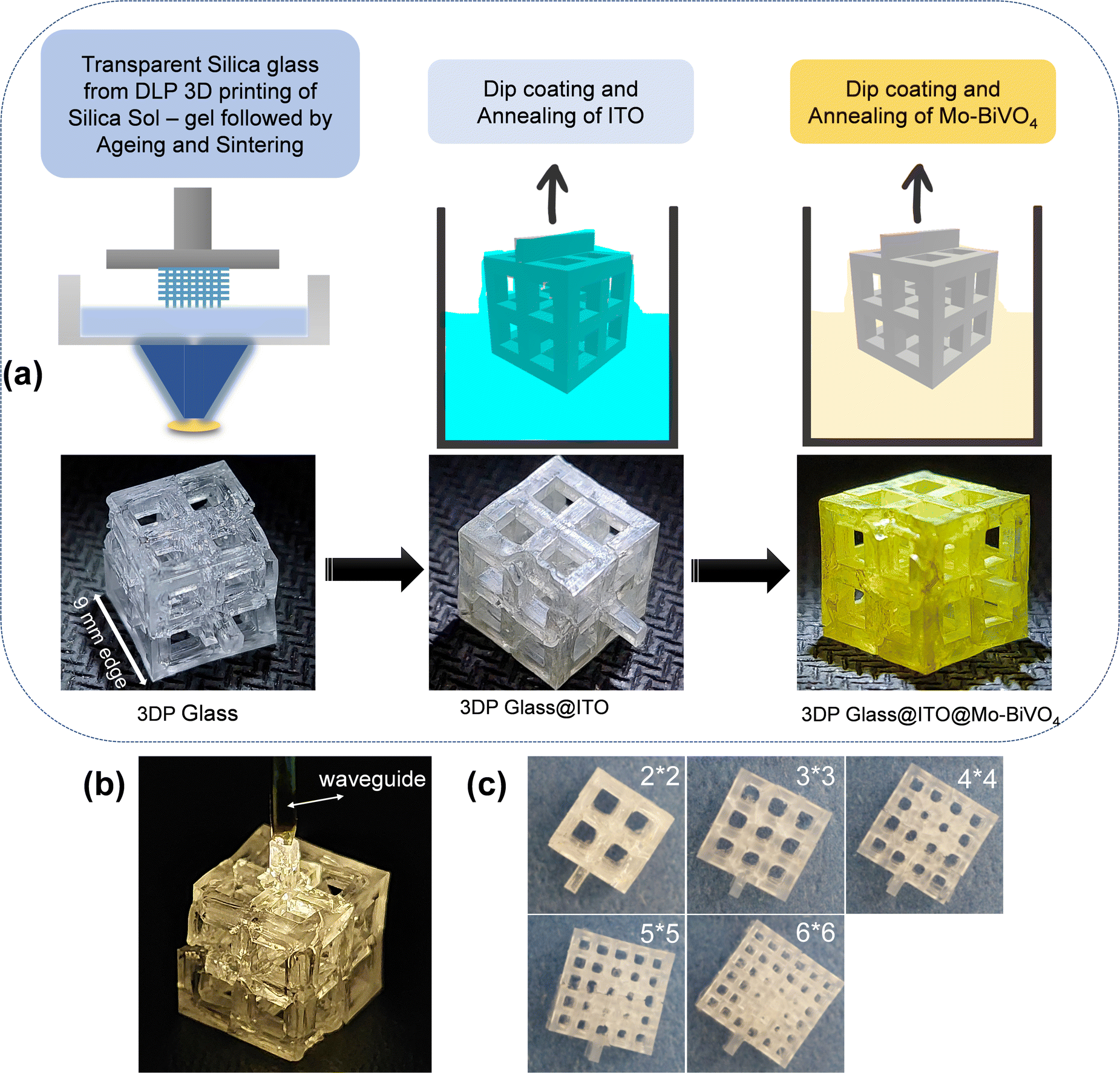 | ||
| Fig. 1 (a) Illustration of the fabrication of semi-transparent 3D lattice structures for photoelectrochemical water oxidation. (b) Picture of the 3D printed glass in a dark room with a light waveguide joined at the tip of the lattice to demonstrate waveguiding of the light through the lattice structure. (c) Picture of the 3D printed glass lattice structures with varying degrees of porosity; all the printed lattices have the dimension of a 9 mm × 9 mm × 9 mm cube. | ||
Hence the 3D printed 2 × 2 lattice has the dimensions of a 9 mm cube with an array of 2 × 2 square holes of 2.57 mm edge length and beams of 1.28 mm edge length, while the 3D printed 6 × 6 lattice has an array of 6 × 6 holes of 0.95 mm edge length and beams of 0.475 mm edge length on each face of the cube. Hence, the 6 × 6 lattice is the most porous while the 2 × 2 lattice is the least porous of all the samples. The final printed samples of each of these lattice structures are shown in Fig. 1c for illustration. The 3D printed lattice structures are transparent and are capable of waveguiding the light through their lattice as shown in Fig. 1b. This property is very useful in capturing solar energy by PEC electrolyzers, which are located even within partial enclosures or remote locations (e.g., within buildings) by waveguiding the light to the entire lattice from selected entry points.
The next step is to make the lattice structures conductive. Non-directional dip-coating of ITO was used instead of the directional vacuum method due to the 3D lattice structure. This step is very critical as the ITO coating should be sufficiently uniform and thick to be conductive32 but not excessive when the coatings start to become opaque, thus reducing the transparency of the glass substrate. To achieve a conductive coating with good transparency we performed parameter optimization of the dip coating. A solution of InCl3 and SnCl2 in IPA was chosen for this as IPA is highly volatile and the solution was found to be stable for several weeks. A constant dip coating speed of 1 mm s−1 and solutions with varying concentrations from 0.1 M to 0.4 M were chosen for this investigation. For multiple coatings the coated glass was placed in a furnace at 600 °C for 5 minutes, before being removed from the furnace and cooled down followed by subsequent layering of the coating. During each coat and 5 minute anneal, the salts (InCl3 + SnCl2) coated on the substrate reacted to form the ITO thin films.
This was necessary to form a homogenous coating. If a high concentration of precursor salts (InCl3 + SnCl2) is deposited and annealed, it leads to a lack of adhesion between the substrate and the coating. Fig. 2a and b shows the variation of sheet resistance and optical transparency with an increasing number of dip coats for various solution concentrations. The numerical values of sheet resistance and transparency (at 550 nm) are listed in Tables S1 and S2 (ESI†). Optical images of the dip-coated glass samples are shown in Fig. 2c to understand the transparency of these samples. At a very low concentration (0.1 M) the sheet resistance is in the order of many thousands of Ohms per sq. although they show very high transparency (>95%). On increasing the solution concentration to 0.4 M a drastic reduction in sheet resistance was observed with a gradual decrease in optical transparency as well. We found the concentration of 0.4 M to be most suitable where a sheet resistance as low as 340 Ohm per sq. was achieved at an optical transparency of 82%. Increasing the solution concentration to 0.5 M reduces the transparency to below 75%, so we decided to use 0.4 M as our most optimized condition. The optical image of the ITO-coated 3D printed lattice structure is shown in Fig. 1a.
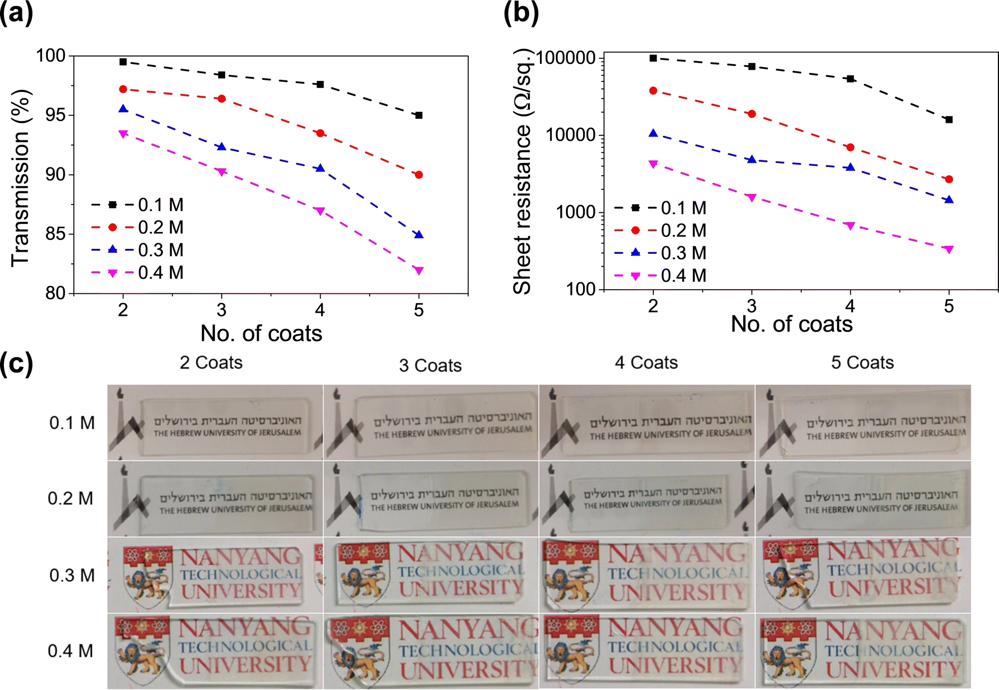 | ||
| Fig. 2 Plots showing the effect of the concentration of the dip coating solution and the number of dip coats of ITO on the (a) percentage transmittance at 550 nm, (b) sheet resistance (in Ohms per sq.). (c) Optical images of the flat glass substrates dip coated with ITO with different numbers of coatings (from 2 to 5) and different concentrations (0.1 M to 0.4 M) of the coating solution. | ||
The top view FESEM image (Fig. 3a) reveals uniform coverage of the ITO thin films on the glass substrate. Further, the cross-section image (Fig. 3b) reveals an ITO thin film coating of ∼300 nm over the glass substrate. Subsequently, Mo (2%) doped BiVO4 (Mo–BiVO4) thin films were coated onto the ITO-coated substrates according to our previous report.31 We chose Mo–BiVO4 as a photoanode for this study since this material is reported to show good photoactivity6,31,33,34 and stability for water oxidation. Briefly, a 0.03 M solution of Bi, V and Mo salts was dissolved in a solvent mixture of ethanol, acetic acid and DMF. Dip coating was performed 4 times with 5 minute short-term annealing at 450 °C between each coat. The top view FESEM image (Fig. 3c) reveals the uniform coating of the Mo–BiVO4 thin films on the glass/ITO surface. The thickness of the ITO/Mo–BiVO4 thin film is ∼420 nm as seen from the cross section FESEM image in Fig. 3d. The ITO/Mo–BiVO4 thin films on the 3D printed lattice structures also have a similar thickness in the range of 450 nm–500 nm as observed from the FESEM cross section images in Fig. S1 (ESI†). Imaging the cross section of the 3D lattice structure is difficult, and as a result, we only have an estimated thickness of the thin film flakes coming off the surface. Nonetheless, there is no significant difference in the thickness of ITO/Mo–BiVO4 across the 3D printed and flat glass samples which might impact the investigation of the PEC performance here.
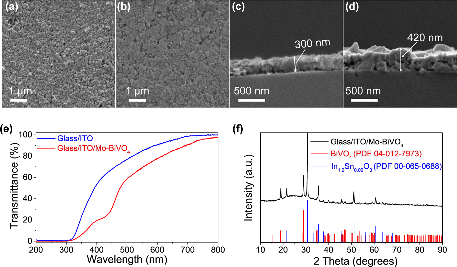 | ||
| Fig. 3 FESEM images showing the morphology and thickness of the thin film. Top view image of (a) glass/ITO, (b) glass/ITO/Mo–BiVO4, and a cross section image of (c) glass/ITO, (d) glass/ITO/Mo–BiVO4. (e) UV-Vis spectra of glass/ITO compared to glass coated with ITO and Mo–BiVO4. (f) X-ray diffraction spectra of glass/ITO/Mo–BiVO4. | ||
An X-ray diffraction test was conducted to study the phase of the ITO and BiVO4 thin films. The diffractogram of the glass/ITO/Mo–BiVO4 thin films in Fig. 3f reveals peaks corresponding to ITO which match with cubic In0.9Sn0.09O3 (PDF #00-065-0688) and peaks of Mo–BiVO4 that match with monoclinic BiVO4 (PDF #04-012-7973) confirming the successful formation of these thin films. The UV-Vis spectra in Fig. 3e compares the transmittance % of the glass/ITO substrate against glass/ITO/Mo–BiVO4 revealing ∼82% transmission for the ITO coated films which reduces to ∼70% upon Mo–BiVO4 coating. The optical images of glass/ITO/Mo–BiVO4 and 3DP silica/ITO/Mo–BiVO4 are shown in Fig. S2 (ESI†) and Fig. 1 respectively, which give an idea of their optical transparency.
After optimizing the coating of ITO and Mo–BiVO4 the fabricated electrodes were tested for their performance in water oxidation. Since the 3D printed lattice structures occupy a volume of ∼1 cm−3 we compared the activity of the 3D printed lattice structures with a group of 3 flat glass (3FG) electrodes assembled one behind another within a 1 cm−3 volume to have a fair comparison. The flat PEC electrodes were bifacially fabricated with the same ITO/Mo–BiVO4 architecture. The linear sweep voltammetry curves with chopped light illumination in Fig. 4a show the current densities furnished by various 3D printed lattices in comparison with flat electrodes. The volumetric current density of the different lattices increase in the following order: 3FG (0.58 mA cm−3) < 2 × 2 lattice (0.76 mA cm−3) < 6 × 6 lattice (0.9 mA cm−3) < 5 × 5 lattice (0.95 mA cm−3) < 3 × 3 lattice (1.18 mA cm−3) < 4 × 4 lattice (1.39 mA cm−3). We also calculated the photocurrent density based on the orthogonally projected surface area (Fig. S8, ESI†) of the 3D lattice, to compare the performance of various lattices. As seen from Fig. S9 ESI,† the current density for various lattices exhibits the following trend: 3FG (0.58 mA cm−2) < 2 × 2 lattice (1.13 mA cm−2) < 6 × 6 lattice (1.49 mA cm−2) < 5 × 5 lattice (1.55 mA cm−2) < 3 × 3 lattice (1.84 mA cm−2) < 4 × 4 lattice (2.23 mA cm−2). The trend is similar to the trend of the presented volumetric current density. Thus, even the least porous 2 × 2 lattice structure furnishes a higher current density than the 3 flat glass electrodes. This should not come as a surprise since the surface area of the 3FG electrodes is around 6 cm−2, while the exposed surface of the 2 × 2 lattice is around 8.56 cm−2. Thus, the higher surface area35 of the 3D printed lattice structures boosts the photocurrent produced per unit volume. Herein, it is worth noting that the photocurrent produced is lower than for the reported BiVO4 systems in the literature. Our experimental investigations reveal that the main reason for this trend is due to the use of dip coated ITO electrodes (sheet resistance – 340 Ohms per sq) as compared to commercial FTO coated (sheet resistance – 13 Ohms per sq) electrodes, which are majorly reported in the literature. In our case as well, when we dip coat Mo–BiVO4 on commercial FTO coated glass substrates, we observe a photocurrent density of 0.75 mA cm−3 which is much higher than the 3 bifacially coated glass/ITO/Mo–BiVO4 electrodes as seen in Fig. S4 (ESI†). Therefore, if our 3D printed lattice structures are coated with FTO by using a commercial CVD system we expect to achieve extremely high current densities.
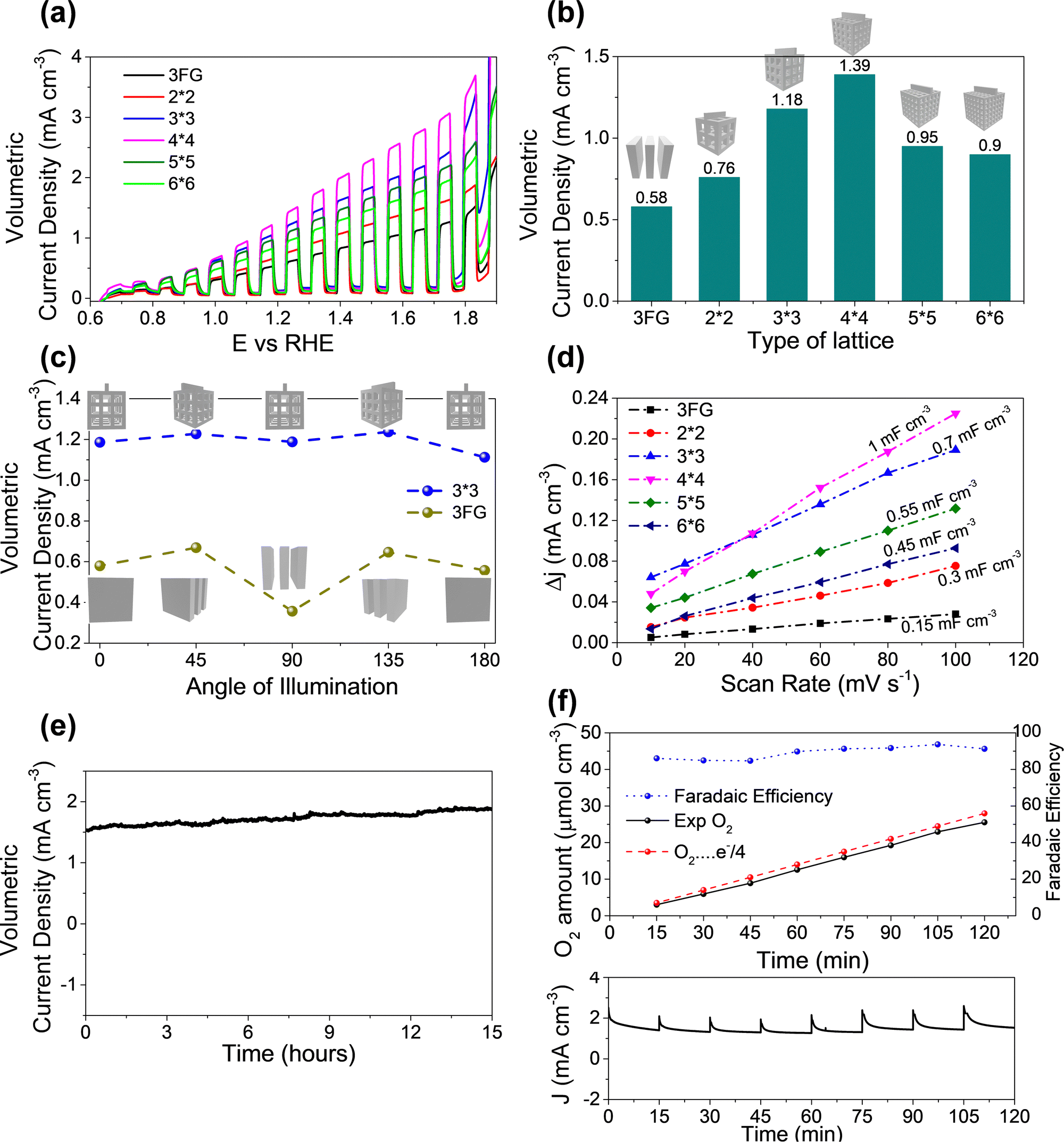 | ||
| Fig. 4 (a) Comparison of linear sweep voltammetry curves of various 3D printed lattices against the 3 flat glass (3FG) samples in series for electrochemical water oxidation under chopped illumination. (b) Comparison of volumetric current density at 1.23 V for various 3D printed lattices and the 3FG samples. (c) Plot of volumetric current density of the 3D printed (3 × 3) lattice and the 3FG samples at 1.23 V at various angles of illumination. (d) Plot of capacitive current (janodic− jcathodic) (at 0.8 V vs. Ag/AgCl) vs. scan rate for various lattices. (e) Plot of observed volumetric current density of the 3D printed (3 × 3) lattice sample for the long term stability test for 15 hours at a constant voltage of 1.5 V. (f) Measured O2 evolution and faradaic efficiency of the 3DP (3 × 3) lattice at 1.5 V vs. RHE for 120 minutes. All the tests were conducted in the 0.1 M KH2PO4/K2HPO4 (pH = 7) buffer solution. | ||
The current density for the 3 × 3 lattice (1.18 mA cm3) reaches even higher values, and the highest current density was observed for the 4 × 4 lattice (1.39 mA cm−3). Thus the 4 × 4 lattice is able to achieve nearly 2.4 times the current density of the flat glass electrodes for the same volume which reveals the advantages of using the lattice structured electrodes for PEC. However, a further increase in porosity in the case of the 5 × 5 and 6 × 6 lattices resulted in a decrease in photocurrent compared to the 3 × 3 and 4 × 4 lattices despite them having a higher surface area. To investigate the above anomaly, electrochemical active surface (ECSA) measurements were conducted by cyclic voltametry tests. The slope of the plot of capacitive current at 0.8 V vs. Ag/AgCl electrode (Fig. 4d) gives the double layer capacitance (Cdl) of the electrode which is a good estimate of ECSA. The double layer capacitance follows the following trend: 4 × 4 (1 mF cm−3) > 3 × 3 (0.7 mF cm−3) > 5 × 5 (0.55 mF cm−3) > 6 × 6 (0.45 mF cm−3) > 2 × 2 (0.3 mF cm−3) > 3FG (0.15 mF cm−3). Evidently, with an increase in porosity from the 2 × 2 to the 4 × 4 lattice the Cdl also increases. Thus, the increase in ECSA contributes to an increase in the number of active sites which results in a higher photocurrent as observed during the experiments. However, the trend changes for the 5 × 5 and 6 × 6 lattices. Although both the 5 × 5 and 6 × 6 lattices have more geometrical area in principle, their ECSAs are lower than those of the 4 × 4 and 3 × 3 lattices. Fig. 1c gives a probable reason for this. As the porosity of the lattice structures increased, there was some over-curing of the sol–gel observed during 3D printing in case of the 5 × 5 and 6 × 6 lattices which resulted in closing of the pores in the central part of the lattice. Further, the struts of these lattice structures have small dimensions of 0.474 mm and 0.563 mm, and the pores have dimensions around 0.95 mm and 1.125 mm for the 6 × 6 and 5 × 5 lattice structures respectively. We guess that the dip coating of ITO and Mo–BiVO4 may not have been as effective as for the other lattices due to the non-uniform coverage of the thin films due to surface tension effects during dip coating and drying. We believe that there is an opportunity for further improvement in the photocurrent density through further optimization of the 3D printing parameters and dip coating techniques. However, that would entail appropriate tweaking of the sol–gel for 3D printing and surface treatment of the lattice structures and reducing the surface tension of the dip coating solution through an appropriate choice of surfactants without affecting the thin film deposition. These studies however are beyond the scope of this work and would be explored separately. Further, the use of porous lattice electrodes may raise the concern of mass transport during PEC electrolysis. To investigate this, PEC water oxidation was conducted at 2 V (vs. RHE) for 60 minutes on both a flatbed and 3D printed lattice (3 × 3) electrode. If the mass transport in the 3D lattice electrodes is bad, it can be observed from a reduction in the current density over time, due to increased gas bubble accumulation at the electrode surface. However, as observed from Fig. S7 in the ESI† there was no reduction in current observed for both the flatbed and 3D lattice structure electrodes, during electrolysis at 2 V for 60 minutes. Since the volumetric current density is well below 10 mA cm−3 we assume that there is no accumulation of the products at the electrodes. We also would like to point out that at 2 V bias in direct electrolysis, most well-reported catalyst systems36,37 reach more than 100 mA cm−2 current density, where using the PEC system is impractical. To conclude, in the case of PEC electrolysis where practical application is at low voltages or zero bias, the impact of increasing the surface area (by making porous electrodes) has a larger positive impact on boosting the performance than a probable reduction in activity due to the mass transport phenomenon.
Following on, the impact of the solar radiation angle on the PEC performance for the 3D printed lattices and traditional flat glass substrates was investigated. Among the 3D printed samples the 3 × 3 lattice was structurally strong and stable, while the 4 × 4 lattice was more brittle. Therefore, the 3 × 3 lattice was chosen for further investigations on the impact of the angle of illumination and the stability test. The electrodes were rotated from 0 degrees to 180 degrees with respect to the solar simulator and the photocurrent at 1.23 V was measured. Here, 0 degrees refers to illumination perpendicular to the flat glass substrate and 90 degrees (refer to Fig. S5 (ESI†) for the setup) is when the flat glass is parallel to the direction of illumination (see the inset of Fig. 4c for details). The 3FG electrodes achieved photocurrent densities of 0.58, 0.67, 0.36, 0.64, and 0.56 mA cm−3 for angles of illumination of 0, 45, 90, 135, and 180 degrees. There is a slight increase in the current densities at 45 degrees and 135 degrees because the inner electrode surfaces are directly illuminated, effectively leading to a larger illumination area. However, at 90 degrees the photocurrent is reduced by nearly 38% to 0.36 mA cm−3 since only a small area is directly illuminated. However, in case of the 3 × 3 3D printed lattice, the change of the volumetric photocurrent densities was marginal. The observed current densities are 1.18, 1.22, 1.18, 1.23, and 1.11 mA cm−3 for 0, 45, 80, 135 and 180 degrees respectively. Here also, at 45 and 135 degrees, there is an increase in photocurrent density due to a higher exposed surface area to illumination, but the difference is within 6%. This is because the surface area of illumination at all angles is nearly the same due to the 3D design of the lattice structures which have exposed struts at every angle of illumination. Further, the variation of current density (based on orthogonally projected area) for the flat glass and the 3 × 3 lattice samples for different angles of illumination is shown in Fig. S9b ESI.† Evidently, for the 3 × 3 lattice the current density at 45 degrees is lower since the increase in current is not proportional to the increase in projected surface area. However, as discussed before, the absolute or volumetric current density at 45 degrees is higher than at 0 degrees, since a larger area of the struts is exposed to direct illumination of light at 45 degrees compared to 0 degrees. For the flat glass samples, although the current density at 90 degrees is higher than at other angles, the total current is small, since the area is very small. So, the projected area current density does not accurately describe the device performance. Hence, in this report, we have used volumetric current density as a basis for comparison of the performance. Herein, we wish to highlight that solar light intensity changes through the day and hence impacts the photocurrent. To investigate the effect of incident light intensity on the photocurrent, the above tests were repeated for three other light intensities, i.e., 75 mW cm−2, 50 mW cm−2, and 25 mW cm−2. The photocurrent density was reduced with lower light intensity and follows a similar trend for different angles of illumination. For instance, the 3D printed lattice structure electrode (3 × 3) produces (Fig. S6 in ESI†) photocurrents of 0.81 mA cm−3, 0.45 mA cm−3, and 0.28 mA cm−3 at 75 mW cm−2, 50 mW cm−2, and 25 mW cm−2 respectively at zero angle of illumination. In the case of the flatbed electrodes photocurrents of 0.35 mA cm−3, 0.17 mA cm−3, and 0.10 mA cm−3 are produced at 75 mW cm−2, 50 mW cm−2, and 25 mW cm−2 respectively. In summary, the 3D printed lattice structure electrodes are minimally affected by the changing angle of illumination as compared to the flatbed electrodes.
It is worth highlighting that throughout this investigation we have considered volumetric current density (mA cm−3) instead of current density based on surface area (mA cm−2) to compare the performance of the flatbed electrodes with the 3D lattice structured electrodes. This is because our electrodes are three dimensional and quantifying the exact surface area under illumination is not feasible. Further, at the device level what matters more is the total photocurrent produced by the device rather than the current density. The total current produced however is dependent on the size of the device, hence we have chosen volumetric current density for comparison of the performance. In other words at the device level, irrespective of the photocatalyst used, the 3D printed lattice structures coated with a photocatalyst produce larger photocurrents (higher gas evolution) compared to the flatbed electrodes for a given volume, and show minimal changes in photocurrent with the changing angle of illumination. Thus, for on-site applications, the 3D lattice structured electrodes are a better alternative to flat electrodes. Going further, a 15 hour stability test was carried out for the 3D printed 3 × 3 lattice (Fig. 4e) by applying a bias of 1.5 V and measuring the photocurrent for 15 hours. No observable decrease in the photocurrent densities over 15 hours shows the stability of the electrode, and the photoanode for long term usage. The amount of oxygen produced was also quantified using gas chromatography to estimate the faradaic efficiency of the 3D printed lattice structure electrodes. Approximately 25.53 μmol cm−3 of O2 gas was produced in 120 minutes of PEC electrolysis conducted at 1.5 V with a faradaic efficiency of ∼91.24%. The calculated faradaic efficiency was above 84% for all the measured intervals revealing that the majority of the current is used in gas evolution.
We have demonstrated the proof of concept of using 3D printed lattice structure electrodes for PEC applications. However, we have only explored simple cubic structures in this investigation. 3D printing enables the fabrication of even more complex structures which have a much higher surface area and different exposed surfaces which could benefit from both solar light absorption as well as the easier release of gas bubbles formed during the electrolysis. Further numerical and experimental investigations are necessary for designing lattice structures that furnish a large surface area for solar radiation capture, and simultaneously allow for better transmission of solar radiation into the inner layers of the lattice structures. We also propose the use of the 3D printed transparent lattices in the manufacture of enclosed solar energy capture devices. PEC electrolyzers and other solar energy capturing devices might need to be enclosed due to safety and manufacturing limitations. Since the 3DP lattices have a waveguiding ability, these enclosed devices can be coupled with light guides that bring solar light into these devices at specific inlets instead of needing to expose the entire device to an open atmosphere for exposure to the Sun.
Conclusions
This study was conducted due to the exciting possibilities of incorporating 3D lattice electrodes for photoelectrochemical water splitting. We successfully fabricated 3D lattice electrodes through DLP 3D printing of photopolymerizable compositions with sol–gel precursors to prepare transparent lattice structures. These lattice structures were coated with ITO and Mo–BiVO4 thin films which made them superior electrodes for PEC water oxidation. Through parameter optimization of the dip-coating of ITO we could fabricate transparent conductive electrodes with ∼82% transparency while having a low sheet resistance of 340 Ohms per sq. Further, the 3D printed electrodes showed ∼2.4 times the photocurrent density per unit volume than the flat glass electrodes, revealing the advantages of using 3D printed electrodes. Also, the 3D printed electrodes showed a negligible change in performance for changes in the angle of illumination, compared to commonly reported flat glass electrodes, thus establishing their clear preference for use in on-site electrolyzer deployment. This study will open up further scientific and engineering advancements in the field of 3D electrode design for photoelectrocatalysis.Author contributions
L. H. W. and S. M. proposed the project, conceived the idea, brought the funding, and supervised the entire project. C. H. conducted experiments, analyzed the data and wrote the manuscript. T. R. helped in optimization of the 3D printing sol-gel ink. J. M. R. T. assisted in the experiments. All the authors reviewed the manuscript.Conflicts of interest
There are no conflicts to declare.Acknowledgements
This work was supported by the Singapore Ministry of Education (MOE) Tier 2 grant (MOE T2EP50120-00081) and Tier 1 grant (2020-T1-001-147 (RG64/20)). This research was also supported by the National Research Foundation, Prime Minister's Office, Singapore under its Campus of Research Excellence and Technological Enterprise (CREATE) programme. The authors acknowledge funding received from the Israel Ministry of Science and Technology and a scholarship donation by Susan Lawi. The authors also like to acknowledge the Facility for Analysis, Characterization, Testing, and Simulation (FACTS), Nanyang Technological University, Singapore, and the Center for Nanoscience and Nanotechnology of the Hebrew University of Jerusalem, for use of electron microscopy and XRD facilities.References
- D. Ferrero, M. Gamba, A. Lanzini and M. Santarelli, Energy Procedia, 2016, 101, 50–57 CrossRef CAS
.
- J. A. Turner, Science, 2004, 305(5686), 972–974 CrossRef CAS PubMed
- M. Rohloff, B. Anke, S. Zhang, U. Gernert, C. Scheu, M. Lerch and A. Fischer, Sustainable Energy Fuels, 2017, 1, 1830–1846 RSC
- C. Jiang, S. J. A. Moniz, A. Wang, T. Zhang and J. Tang, Chem. Soc. Rev., 2017, 46, 4645–4660 RSC
- T. Xia, M. Chen, L. Xiao, W. Fan, B. Mao, D. Xu, P. Guan, J. Zhu and W. Shi, J. Taiwan Inst. Chem. Eng., 2018, 93, 582–589 CrossRef CAS
- B. Zhang, H. Zhang, Z. Wang, X. Zhang, X. Qin, Y. Dai, Y. Liu, P. Wang, Y. Li and B. Huang, Appl. Catal., B, 2017, 211, 258–265 CrossRef CAS
- T. H. Nguyen, M. Zhang, W. Septina, M. G. Ahmed, Y. F. Tay, F. F. Abdi and L. H. Wong, Solar RRL, 2020, 4, 2000437 CrossRef CAS
- K. H. Ye, H. Li, D. Huang, S. Xiao, W. Qiu, M. Li, Y. Hu, W. Mai, H. Ji and S. Yang, Nat. Commun., 2019, 10, 3687 CrossRef PubMed
- K. Sivula, F. Le Formal and M. Gratzel, ChemSusChem, 2011, 4, 432–449 CrossRef CAS PubMed
- K. Maeda, ACS Appl. Mater. Interfaces, 2014, 6, 2167–2173 CrossRef CAS PubMed
- K.-H. Ye, Z. Wang, H. Li, Y. Yuan, Y. Huang and W. Mai, Sci. China Mater., 2018, 61, 887–894 CrossRef CAS
- K. Y. Yoon, J. Park, M. Jung, S. G. Ji, H. Lee, J. H. Seo, M. J. Kwak, S. Il Seok, J. H. Lee and J. H. Jang, Nat. Commun., 2021, 12, 4309 CrossRef CAS PubMed
- M. Zhang, R. P. Antony, S. Y. Chiam, F. F. Abdi and L. H. Wong, ChemSusChem, 2019, 12, 2022–2028 CrossRef CAS PubMed
- A. S. J. Wardhana, E. S. Damarwan and M. L. Hakim, J. Phys.: Conf. Ser., 2021, 2111, 012053 CrossRef
- M. Nfaoui and K. El-Hami, Int. J. Ambient Energy, 2018, 41, 214–223 CrossRef
- M. K. Sharma, D. Kumar, S. Dhundhara, D. Gaur and Y. P. Verma, Global Challenge, 2020, 4, 1900109 CrossRef PubMed
- J. Ahn, Y. S. Park, S. Lee, J. Yang, J. Pyo, J. Lee, G. H. Kim, S. M. Choi and S. K. Seol, Sci. Rep., 2022, 12, 346 CrossRef CAS PubMed
- H. Wang, L. Y. Liu, P. Ye, Z. Huang, A. Y. R. Ng, Z. Du, Z. Dong, D. Tang and C. L. Gan, Adv. Mater., 2021, 33, e2007072 CrossRef PubMed
- J. F. Destino, N. A. Dudukovic, M. A. Johnson, D. T. Nguyen, T. D. Yee, G. C. Egan, A. M. Sawvel, W. A. Steele, T. F. Baumann, E. B. Duoss, T. Suratwala and R. Dylla-Spears, Adv. Mater. Technol., 2018, 3, 1700323 CrossRef
- D. Zhang, X. Liu and J. Qiu, Front. Optoelectron., 2020, 14, 263–277 CrossRef PubMed
- I. Cooperstein, E. Shukrun, O. Press, A. Kamyshny and S. Magdassi, ACS Appl. Mater. Interfaces, 2018, 10, 18879–18885 CrossRef CAS PubMed
- I. Cooperstein, E. Sachyani-Keneth, E. Shukrun-Farrell, T. Rosental, X. Wang, A. Kamyshny and S. Magdassi, Adv. Mater. Interfaces, 2018, 5, 1800996 CrossRef
- E. Shukrun, I. Cooperstein and S. Magdassi, Adv. Sci., 2018, 5, 1800061 CrossRef PubMed
- R. A. Marquez, K. Kawashima, Y. J. Son, R. Rose, L. A. Smith, N. Miller, O. A. Carrasco Jaim, H. Celio and C. B. Mullins, ACS Appl. Mater. Interfaces, 2022, 14, 42153–42170 CrossRef CAS PubMed
- X. Su, X. Li, C. Y. A. Ong, T. S. Herng, Y. Wang, E. Peng and J. Ding, Adv. Sci., 2019, 6, 1801670 CrossRef PubMed
- C. Iffelsberger, D. Rojas and M. Pumera, J. Phys. Chem. C, 2022, 126, 9016–9026 CrossRef CAS
- I. Cooperstein, S. Indukuri, A. Bouketov, U. Levy and S. Magdassi, Adv. Mater., 2020, 32, e2001675 CrossRef PubMed
- D. G. Moore, L. Barbera, K. Masania and A. R. Studart, Nat. Mater., 2020, 19, 212–217 CrossRef CAS PubMed
- F. Kotz, K. Arnold, W. Bauer, D. Schild, N. Keller, K. Sachsenheimer, T. M. Nargang, C. Richter, D. Helmer and B. E. Rapp, Nature, 2017, 544, 337–339 CrossRef CAS PubMed
- H. Liu, Y. Zhang, X. Zhang, Q. Wang, H. Wang, S. Zhang, Y. Ma, Y. Cui, W. Ding and C. Dong, J. Alloys Compd., 2020, 836, 155514 CrossRef CAS
- R. P. Antony, M. Zhang, K. Zhou, S. C. J. Loo, J. Barber and L. H. Wong, ACS Omega, 2018, 3, 2724–2734 CrossRef CAS PubMed
- T. Ito, H. Uchiyama and H. Kozuka, Langmuir, 2017, 33, 5314–5320 CrossRef CAS PubMed
- H. Jung, S. Y. Chae, H. Kim, B. K. Min and Y. J. Hwang, Catal. Commun., 2016, 75, 18–22 CrossRef CAS
- X. Zhao, J. Hu, S. Chen and Z. Chen, Phys. Chem. Chem. Phys., 2018, 20, 13637–13645 RSC
- Z. W. Seh, J. Kibsgaard, C. F. Dickens, I. Chorkendorff, J. K. Norskov and T. F. Jaramillo, Science, 2017, 355, eaad4998 CrossRef PubMed
- V. A. Beck, A. N. Ivanovskaya, S. Chandrasekaran, J. B. Forien, S. E. Baker, E. B. Duoss and M. A. Worsley, Proc. Natl. Acad. Sci. U. S. A., 2021, 118, e2025562118 CrossRef CAS PubMed
- Y. Luo, Z. Zhang, M. Chhowalla and B. Liu, Adv. Mater., 2022, 34, e2108133 CrossRef PubMed
Footnote |
| † Electronic supplementary information (ESI) available. See DOI: https://doi.org/10.1039/d2mh01475k |
| This journal is © The Royal Society of Chemistry 2023 |