
 Open Access Article
 This Open Access Article is licensed under a Creative Commons Attribution-Non Commercial 3.0 Unported Licence
Preparation, properties and applications of two-dimensional superlattices
Fei
Xing†
a,
Guangmin
Ji†
a,
Zongwen
Li†
a,
Weiheng
Zhong
b,
Feiyue
Wang
d,
Zhibo
Liu
 *c,
Wei
Xin
*b and
Jianguo
Tian
c
*c,
Wei
Xin
*b and
Jianguo
Tian
c
aSchool of Physics and Optoelectronic Engineering, Shandong University of Technology, Zibo, 255049, China
bKey Laboratory of UV-Emitting Materials and Technology, Ministry of Education, Northeast Normal University, Changchun, 130024, China. E-mail: xinwei@nenu.edu.cn
cKey Laboratory of Weak Light Nonlinear Photonics, Ministry of Education, Teda Applied Physics Institute and School of Physics, Nankai University, Tianjin, 300071, China. E-mail: liuzb@nankai.edu.cn
dState Key Laboratory of Optoelectronic Materials and Technologies, School of Electronics and Information Technology, Sun Yat-sen University, Guangzhou, 510275, China
First published on 10th December 2022
Abstract
As a combination concept of a 2D material and a superlattice, two-dimensional superlattices (2DSs) have attracted increasing attention recently. The natural advantages of 2D materials in their properties, dimension, diversity and compatibility, and their gradually improved technologies for preparation and device fabrication serve as solid foundations for the development of 2DSs. Compared with the existing 2D materials and even their heterostructures, 2DSs relate to more materials and elaborate architectures, leading to novel systems with more degrees of freedom to modulate material properties at the nanoscale. Here, three typical types of 2DSs, including the component, strain-induced and moiré superlattices, are reviewed. The preparation methods, properties and state-of-the-art applications of each type are summarized. An outlook of the challenges and future developments is also presented. We hope that this work can provide a reference for the development of 2DS-related research.
 Zhibo Liu | Zhi-Bo Liu is a professor at the Key Laboratory of Weak Light Nonlinear Photonics, Ministry of Education, School of Physics and Teda Institute of Applied Physics, Nankai University, China. He received his PhD degree from Nankai University, China, in 2006. His current research interests include nonlinear optics, 2D materials, and optical sensors. |
 Wei Xin | Wei Xin received his BS (2010) from the Changchun University of Science and Technology and PhD (2017) from Nankai University. After that, he continued his research in the State Key Laboratory of Applied Optics, Changchun Institute of Optics, Fine Mechanics and Physics, Chinese Academy of Sciences. In 2020, he joined Northeast Normal University as an associate professor in the Key Laboratory of UV-Emitting Materials and Technology, Ministry of Education. His research focuses on 2D material-based micro/nanodevices and laser processing. |
1. Introduction
The research on superlattices can be traced back to the late 1960s.1 In order to observe the Bloch oscillation of electrons, people initially predicted and designed a novel material which was periodically arranged with two different semiconductors in a sequence.2 The band alignments of the two require a spatial distribution usually exhibited as a multiple quantum well. The size of each composition is kept only several or tens of times larger than that of the lattice constants but shorter than the de Broglie wavelengths of electrons.3 This makes the overlap between wave functions in adjacent wells more obvious, resulting in the unique properties of carriers different from those in traditional bulk materials and presenting broad application prospects.4,5 This class of materials are called superlattices, and they’ve been getting a lot of attention since they were proposed. New elements are constantly added to push the field forward especially after the appearance of two-dimensional (2D) materials.6,7 The concept of integrating them into a new 2D superlattice (2DS) has given another impetus to their development.8–11In a broader sense, a 2D material refers to a film with atomic thickness in the out-of-plane direction. More than thousand kinds have been predicted so far.12,13 From the perspective of element types forming the layer, 2D materials have been divided into mono- (such as graphene, black phosphorus (BP) etc.) or multiple-element (hexagonal boron nitride (h-BN), transition metal dichalcogenide (TMD) etc.) ones. Regardless of the material, the intralayer atoms are always held together by chemical bonds, and the neighbor layers are bonded to each other by the relatively weak van der Waals (vdW) forces.13–15 This dangling-bond-free lattice makes it technically easy to stack multiple 2D materials arbitrarily, so the forms of 2D “component superlattices” (CSs) are initially designed just in imitation of the traditional layer-by-layer structures.16–19 However, natural advantages of 2D materials in their properties, dimension, diversity and compatibility present more possibilities for their further performance breakthrough. With in-depth research, other types such as the in-plane CS, “strain-induced superlattice” (SS) and “moiré superlattices” (MS) appear one after another.20–23 The performances of carriers in these types are compressed from three to two dimensions. This conceptional expansion is not mechanical duplication but makes use of both the material's properties and structural characteristics at a micro/nano scale. 2DSs contribute to further expanding the performance of electronic components and downscaling the size of related devices, so as to expand Moore's law to the field of optoelectronics.
Fig. 1 gives a brief introduction of the above three typical 2DSs which covers most of the existing structural systems. Their main characteristics can be summarized as follows:
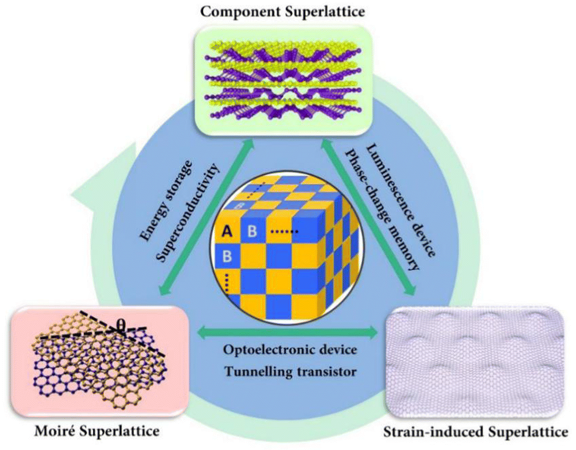 | ||
| Fig. 1 Schematic diagram of 2DSs, including their formations and potential applications. | ||
(1) CS: similar to the structure of traditional superlattice materials, CS is usually arranged by different kinds of 2D materials periodically in the out-of-plane or in-plane directions.19,20 The atomic monoelemental crystals or even their composite films with thicker thicknesses are selected as building blocks depending on the field of applications. This structure is currently the dominant configuration of 2DSs. The interfacial effect and energy band alignment of each element are generally the decisive factors affecting the performance of related devices.
(2) SS: the SS can be considered as an evolution from the basic structure of the CS. When people studied the traditional GaAs/GaAsP superlattice in as early as the 1980s, they found that strain/stress is common and non-negligible, affecting the properties of materials once the lattice mismatch was greater than ∼0.1%.24 With the study of 2D materials being continued recently, it is found that it is impossible to avoid the periodic interfacial buckling especially when the strain in the materials exceeds a critical value (∼2–3%).25,26 In this case, the strain is more important and can induce more novel phenomena. These morphological changes are also accompanied by the introduction of localized fields, which can further modulate the band structures of materials in the in-plane direction.27,28 At present, there are still few reports on SSs and there is no unified standard to define the structures. Whether the band structure of a material is subject to periodic modulation caused by external substances is the main issue here. We collectively refer to the 2DSs with the above characteristics as SSs.
(3) MS: the MS can be considered as a further extension of SS, and recently it has been extensively studied as a separate system.29–32 The MS is usually made by stacking two or more layers of the same or different kinds of 2D materials together with a relative twisted angle (θ) between layers. It causes an interlayer mismatch in the lattice and a periodic angle-dependent moiré potential along with the moiré patterns in a larger area. This potential affects the energy band structure of the system as a whole, leading to the novel physical phenomena different from the traditional superlattices.
Significantly, we can find that there is no complete boundary in the morphology between the above-mentioned different 2DSs. The existence of multiple influencing factors in a certain system can even be observed. Although the final properties of a 2DS are determined synthetically, the dominant role is still relatively clear. As a typical example, when designing a light emitting diode (LED) device by using a CS system, Novoselov's group was more concerned with the influence of energy band alignment and the tunneling movement of carriers in it rather than the effects of lattice mismatch.33 In another experiment, Mao et al. identified the influence of strain and ruled out the moiré potential interpretation even though the moiré patterns were clearly between the G/NbSe2 interfaces.26 Therefore, based on the main factors affecting the properties of 2DSs, we sorted out and discussed the recent work accordingly.
The research on 2DSs is an emerging field. Although there were many published reviews, most of them paid more attention to the properties and applications of a selected type. There is a lack of overview introduction about 2DSs at present. In addition, due to their similar architectures to the 2D heterostructures and metamaterials, there is usually confusion in the discussion of concept of 2DSs. Whether the de Broglie wave of carriers in a material can be effectively modulated by the periodic potential field is an important criterion for judging as a 2DS. Based on this, we summarize the recent research studies and reorganize them from the perspective of preparation, properties and applications of different 2DSs. Following that, the existing challenges and development are also discussed. We hope that this review can provide beneficial reference for the development of follow-up work.
2. Preparation strategies of 2DSs
Preparing high-quality 2DSs is critical because it is the basis for later applications. Natural vdW superlattices can be separated from minerals, but the materials got in this way are usually having single properties.34,35 Artificial 2DSs is still the dominant objective. Inspired by preparation of 2D heterostructures, preparing 2DSs can also follow the top-down and bottom-up synthetic strategy.10,36 The advantage of the former is that we can arrange different materials in order as desired, but it is relatively inefficient and inflexible. In contrast, the latter is simpler but the materials involved are usually limited. How to integrate the advantages in new strategies has always been the focus. Here, by summarizing the common preparation strategies for 2DSs, we briefly introduce three main methods, including the mechanical transfer, gas vapor growth and liquid-assisted engineering. These methods run through the development history of 2DSs and the preparation efficiency and qualities of 2DSs have improved greatly (Fig. 2).37–50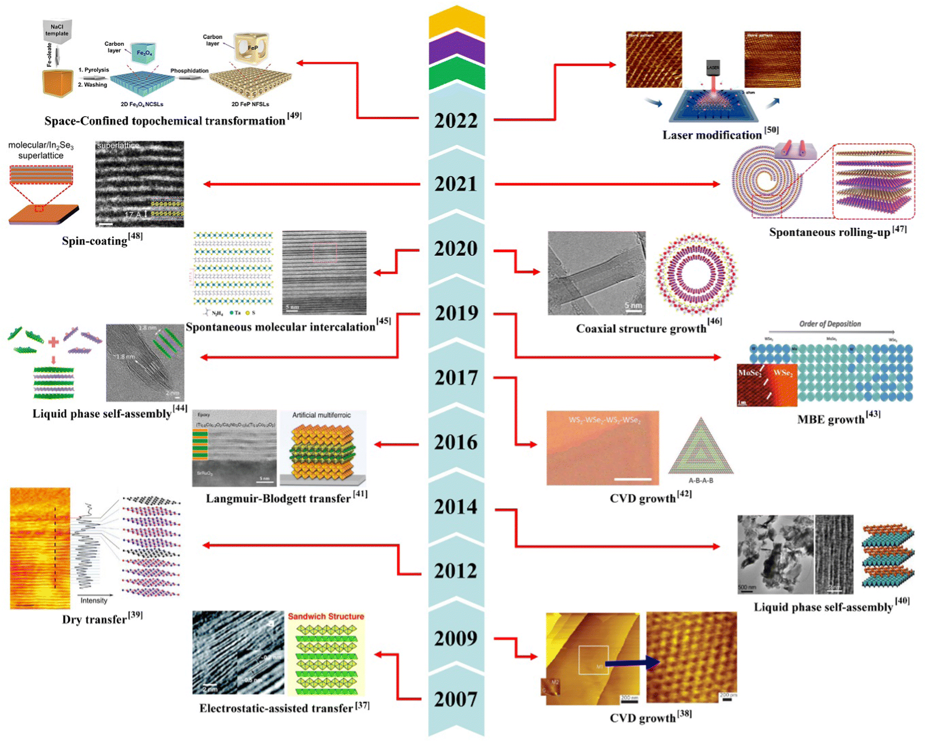 | ||
| Fig. 2 Timeline showing the development of the preparation of 2DSs. Reproduced with permission.37–50 Copyright 2008, 2012, 2013, 2014, 2015, Nature Publishing Group. Copyright 2012, 2013, American Chemical Society. Copyright 2013, 2015, 2016, Wiley-VCH. Copyright 2017, American Association for the Advancement of Science. Copyright 2021, Elsevier. | ||
2.1 Mechanical transfer
Like playing with LEGO, 2D materials can be treated as building blocks and assembled with one-atomic-plane precision as designed.16–18 Generally, two aspects need to be considered during mechanical transfer: high-quality exfoliation of materials and subsequent stacking (Fig. 3a).18 The great success of exfoliating graphene in experiment by Geim et al. encourages people to push the method to improve day by day.12 With continuous technical optimization recently, many techniques, including the liquid exfoliation, gold-assisted exfoliation etc., have emerged one after another.51–55 The variety of materials obtained has been enriched largely under premise of ensuring high lattice quality, and the sample size can range from microns to even centimetres. For example, under the guidance of adhesive energies to gold surface, Gao's group exfoliated more than 40 types of single-crystalline monolayer 2D materials at the same time.54 Both high lattice quality and excellent properties were exhibited.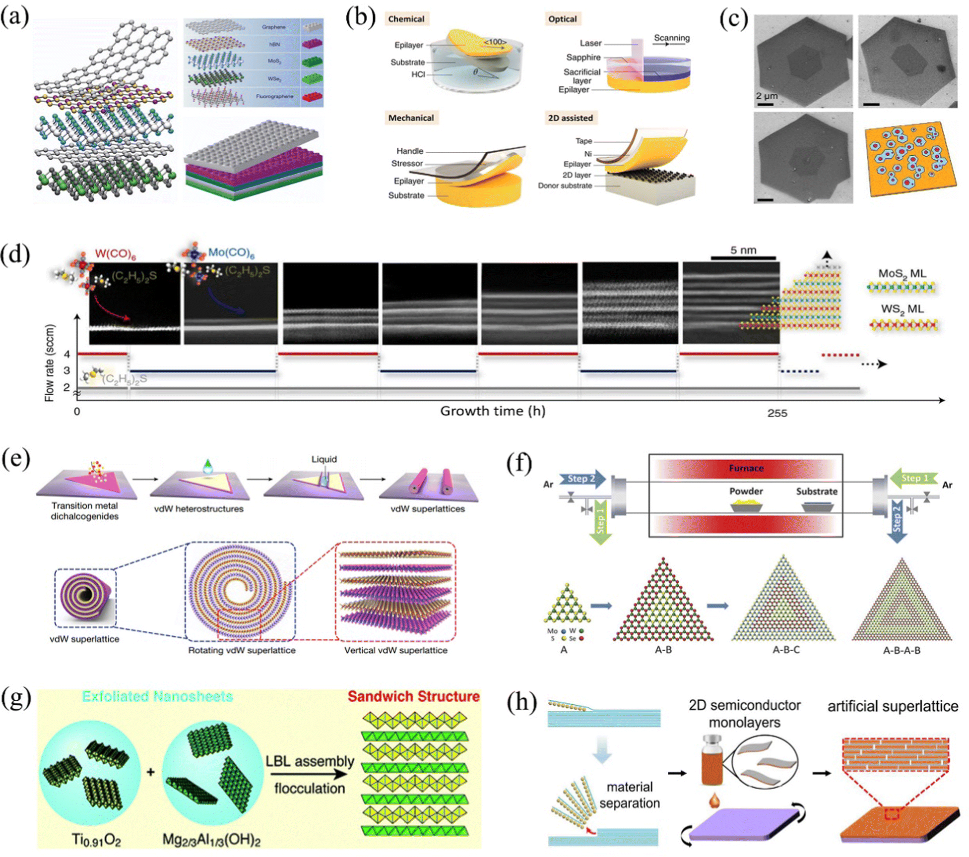 | ||
| Fig. 3 (a) vdWs heterostructures and their Lego block analogies. Reproduced with permission.18 (b) Schematic of common exfoliation-transfer techniques. This process sometimes needs to be assisted by chemical etching or laser heating operations. Reproduced with permission.58 (c and d) Optical and scanning transmission electron microscope (STEM) images of out-of-plane vdWs heterostructure, MS and layer-by-layer CS samples prepared by CVD technique. Reproduced with permission.70,74 (e) Fabrication schematic of the roll-up CSs. Reproduced with permission.47 (f) Growth of in-plane CSs with a modified CVD technique. Reproduced with permission.42 (g) Inorganic-sandwich CSs periodically deposited by layered double hydroxide and oxide nanosheets with a LBL assembly technique. Reproduced with permission.37 (h) Schematic of the assembled tetraheptylammonium bromide-capped In2Se3 monolayers through complete intercalation, separation and spin-coating process. Reproduced with permission.48 Copyright 2013, 2019, 2021, Nature Publishing Group. Copyright 2017, American Association for the Advancement of Science. Copyright 2007, 2013, American Chemical Society. Copyright 2021, Elsevier. | ||
After obtaining the high-quality 2D materials, the next is to stack them artificially. Due to the high degree of spatial freedom, the type, sequence, position or even twisted angle between layers can be controlled well. Taking the preparation of an out-of-plane vdW heterostructure as an example, mechanical transfer generally goes through the following process:56 first, the same type or different types of materials I and II (MI/MII) are exfoliated from its bulk to two pieces of Si/SiO2 substrates, respectively. The MI is chosen as the bottom layer, and the MII as the upper needs to further cover a transition film composed of a water-soluble polymer and a polymethyl methacrylate (PMMA) materials. Second, the silicon slice containing MII is immersed in a bath and the PMMA with MII can be obtained from the water surface after dissolving the polymer. With the help of a microscope operation system, this film can be transferred to another slice to keep MII aligned on top of MI precisely. Finally, the I/II vdW heterostructure is successfully fabricated after dissolving the PMMA in acetone and annealing the sample at a high temperature in a protective gas environment to ensure close contact between the interfaces.
The above procedure can be regarded as the basis for preparing vdW structures. Preparing 2DSs is just an extension of it, and just certain operations need to be adjusted as designed. For example, preparing CSs requires repetition of the procedure, while MSs are concerned more about the twisted angle between the upper and lower materials. As for the SSs that need to undergo buckling transitions between 2D materials or even between materials and substrates, in the mechanical transfer process more attention should be paid to the interlayer coupling, which determines whether the subsequent samples can exhibit excellent properties. To ensure this, in a typical work reported by Andrei's group, a sandwiched graphene/nano-pillar/h-BN structure was annealed overnight in an environment of high temperature and protective gas.57 Recently, with continuous optimization, the quality and efficiency during transfer are improved greatly, making the preparation of 2DSs technically easier (Fig. 3b).58 The liquid surface pressure and surface energy are considered to facilitate large-area and high-quality transfer of materials, and the transition film has been replaced by polydimethylsiloxane (PDMS) or others for reducing residues.59–62 The treatment of the substrate is also one of the important factors affecting the transfer. As an example, with the aid of bubbles and capillary bridges between graphene and substrate, Gao et al. realized the face-to-face transfer of wafer-scale graphene films successfully.63
Mechanical transfer is common in the preparation of vdW structures. It has obvious advantages in the architecture design and implementation in space. Due to the high quality of 2D materials obtained by exfoliation, the heterostructures or even 2DSs prepared in this way usually exhibit excellent properties. However, the complicated operation and low sample yields are the main difficulties. It is mostly confined to the laboratory and fails to integrate with the industrial techniques although the techniques have improved tremendously.50 Combination with other methods is the inevitable trend of future development. For example, recently, Kim's group has reported a programmed crystal assembly technique which combines mechanical transfer and gas vapor growth to prepare wafer-scale 2DSs.64
2.2 Gas vapor growth
Gas vapor growth is one of the most developed methods to prepare large-area, high-quality 2D materials or 2DSs. It is more compatible with existing semiconductor processing techniques, endowing it with great potential for industrial applications, especially in the field of optoelectronics. Here, two important growth techniques, including chemical and physical vapor deposition (CVD, PVD) are reported. Different from the previous method of preparing 2D materials, here we mainly focus on the preparation of 2DSs.For instance, in 2013, Chiu's group reported the preparation of twisted-bilayer graphene (TBG) on Cu foils by using the ambient pressure CVD (AP-CVD) technique for the first time (Fig. 3c).70 By optimizing the environment temperature, gas pressure, and the thickness and purity of the copper foils, the TBG grains and twisted angle between layers can be regulated effectively. Similar operations were also reported by Liu's group.71–73 By further improving the purity of the copper foil while reducing the pressure in the tube furnace, the overlapping region of TBG samples can approach 100 × 100 μm2.72 Besides graphene, in 2014, Liu et al. fabricated the twisted MoS2 bilayers on various substrates.69 In 2021, by precisely controlling the epitaxy kinetics process, Jo's group achieved the layer-by-layer stacking or even arbitrary rotating of TMD materials (Fig. 3d).74 However, decreasing the nucleation rate initially and enriching the variety of stacked materials should be highlighted during the deposition. To solve this problem, Zhao et al. proposed a general strategy a little earlier.47 By dropping an ethanol–water–ammonia solution onto an vdW heterostructure, a force-driven rolling-up higher order CS was synthesized (Fig. 3e). This process is relatively feasible to operate, and extends the concept of superlattices to one dimension, offering more freedom in interlayer coupling for further applications.47,75 In addition to the 2DSs mentioned above, CVD growth also shows good performance for preparing in-plane CSs.20,42,65 In 2015, Li et al. synthesized the monolayer WSe2–MoS2 lateral p–n junction for the first time and observed an atomically sharp interface.68 On this basis, by controlling the reverse flow during temperature swing between successive growth steps, Zhang et al. deposited two types of TMD materials alternatively (Fig. 3f).42 In another report, Xie et al. also synthesized the coherent monolayer 2DSs through a modulated metal–organic CVD method.20 The supercell presented a controllable strain distribution because of the lattice mismatch between materials. In 2020, the concept of ‘in-plane CS’ was further extended to perovskites. By controlling ion diffusion process, Dou's group exhibited an effective method for preparing lateral perovskite 2DS first.76 In addition, the CVD technique also provided coping strategies for preparing SSs. In 2020, by applying the low-pressure CVD (LPCVD) method, Hudson et al. prepared a graphene film on a polished copper foil at 1020 °C.77 After slowly cooling the sample to 80 K, the covered graphene was arranged in periodic ripples to form a SS under the tensile and shear stresses. During this process, the cooling speed and uniformity are important for the latter properties of the SSs.
In general, the biggest advantage of the CVD technique is that it can be used to prepare large-area, high-quality 2DSs, but in the short term, a breakthrough should be made in the synthesis of vertical CS. The improvement on controlling material types, stacking sequences and twisted angles between layers should also be noticed. In addition, as a common problem faced in the CVD technique, achieving the preparation of wafer-scale single crystal is still a focus of research.
2.3 Liquid-assisted engineering
With the help of liquid surface pressure, chemical intercalation agents or external applied voltage, 2D materials can be exfoliated from their bulks in a liquid. By using different deposition techniques subsequently, 2DSs can be synthesized. This process is convenient to operate, but it is always limited by the material types and it is difficult to ensure a good crystal lattice quality at the same time. As an example, here we mainly introduce two techniques: liquid-assisted layer-by-layer deposition (LLD) and solution-phase self-assembly (SSA). They are representative in liquid-assisted engineering of 2DSs.For example, in 2007, Li's group fabricated a composite Ti0.91O2/layered double hydroxide (LDH) superlattice and a Ca2Nb3O10/LDH film by alternately adsorbing the negatively charged metal oxide and the positively charged double hydroxide nanosheets (Fig. 3g).37 The thickness of different components was controlled at 0.6 nm. In contrast, for preparing 2DSs by combining materials with the same charge, a connecting agent such as the polycation/polyanion solution were applied for help. The nanopieces (Ti0.8Co0.2O2 and Ti0.6Fe0.4O2) were connected as 2DSs with the help of poly diallyl dimethyl ammonium chloride.41 The electrostatic adsorption is key but not limited, so the materials for selection are fruitful.85,86 Another important liquid-assisted deposition is the Langmuir–Blodgett transfer technique.87 The nanosheets for deposition are first mixed with an amphiphilic organic compound and then spread over water. The hydrophilic side of the mixture is in contact with the water surface and extends away to the air. A solid-like single-molecule layer can be formed on the liquid surface as a result. By this time, by immersing in and removing out of an appropriate substrate repetitively, 2DSs with multiple components can be obtained. For example, in 2009, Akatsuka et al. successfully produced a high-ordered CS film on a silicon wafer and a quartz glass substrate.88 Li et al. also prepared similar samples on different substrates by using this technique.89
Generally speaking, the SSA technique has progressed greatly in recent years.83 It is simple, efficient and has great development prospects. Compared with the preparation of CS materials, this technique may encounter greater obstacles in preparing MSs and SSs because of the higher requirements for lattice quality. However, a reasonable design is believed to controllably hybridize and prepare target 2DSs with special properties and applications.
3. Properties and applications
In this part, the symbolic properties and recent applications of different types of 2DSs are mainly focused. The properties of 2DSs are jointly determined by the material components and architectures, which provides rich variability and freedom for applications of related devices. It is hard to summarize regularity for this reason, so here only some common characteristics are described.3.1 Properties and applications of CS
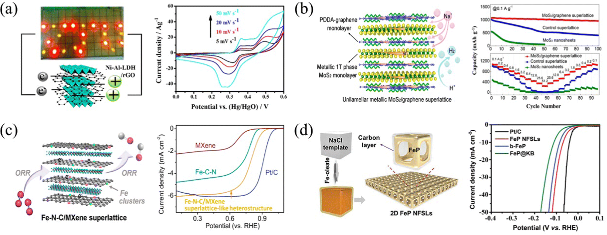 | ||
| Fig. 4 (a) Schematic and cyclic voltammetry (CV) curves of a Ni–Al LDH/rGO CS supercapacitor. Reproduced with permission.95 (b) Schematic of effective sodium storage and hydrogen release through MoS2/graphene CSs. Reproduced with permission.96 (c) Fe-N-C/MXene CS and its electrochemial oxygen reduction reaction plots. Reproduced with permission.97 (d) Preparation process and hydrogen evolution reaction characterization of a 2D FeP nanoframe superlattice. Reproduced with permission.49 Copyright 2016, Elsevier. Copyright 2018, 2020, American Chemical Society. Copyright 2022, Wiley-VCH. | ||
For lithium-ion storage applications, a CS composed of TMOs is ideal because it exhibits better performance as an electrode due to higher storage capacity. Conventional electrodes are usually made of MnO2 nanosheets. They need to undergo a conversion reaction and are inactivated during repeated charge/discharge processes.102 If the sheets are replaced by a graphene/MnO2 CS, the conversion of MnO2 is constrained and the transformants can be confined in 2D channels of graphene materials. This can effectively avoid the capacity decay, greatly improving cycling stability of metal ion storage.103 Similarly, the graphene/MnO2 CSs also performed well in Na-ion storage. The theoretical results showed that the diffusion energy barrier generally decreases as the interlayer distance increases, suggesting that layer-expanded layered materials have higher ion mobility and could achieve faster charge and discharge kinetics.104 Compared with the materials with randomly stacked composites, each layer of nanosheets in the superlattice maintain a large interlayer spacing, which provides more 2D channels for the rapid diffusion of metal ions, thereby obtaining superior rate capability.
The ion diffusivity DGITT can be obtained via the formula
In addition, CSs are also applied to improve the catalytic performance by controlling their electronic motions.109,110 Compared with the bulks, CSs formed by ordered-stacked nanosheets can provide more available active sites and thus exhibit stronger catalytic properties. In 2020, Jiang et al. proposed a metal cluster function in preparing Fe-N-C-/MXene CSs.97 Metal clusters were used to regulate the surface charge of nanosheets, which proves excellent electrocatalytic oxygen reduction reactions (Fig. 4c). Recently, another hydrogen evolution experiment using FeP nanoframe CSs has drawn people's attention.49 Due to unique topochemical transformation processes, the higher efficient and durable electrocatalysts were obtained here compared with the performance of most previous FeP-based catalysts (Fig. 4d). The development of 2DSs provides new opportunities for the design of new advanced materials and catalysts.111
In 2015, Novoselov et al. designed a CS made of few-layered graphene, TMDs and h-BN materials.33 The graphene acted as conductive layers, injecting electrons and holes into the TMDs. The h-BN materials were tunnel barriers (TBs), forming quantum wells (QWs) together with the TMDs on the side. By superimposing QWs and fine controlling over the tunnelling barriers, the carrier's chances of escape are greatly reduced, increasing the luminous efficiency greatly. Here, the quantum efficiency of related devices was ∼8% (Fig. 5a). Similarly, in 2019, Gu et al. combined a h-BN/WS2 CS with a distributed Bragg reflector (DBR) and invested the exciton–polariton electroluminescence (EL) at room temperature (Fig. 5b).112 Due to the strong coupling between CSs and DBR, the external quantum efficiency (EQE) can reach ∼0.1%. In 2020, Lee et al. proposed a coupled QW stacked with alternating h-BN and WS2 to observe its photoluminescence (PL) phenomenon. The h-BN retained interwell interactions dramatically, increasing the exciton energies in quantum traps. Correspondingly, the PL peaks appeared and enhanced linearly with the increase of QW periods.113 In 2021, Kumar et al. also designed CSs composed of periodic TMD/h-BN/Al2O3 materials.114 The luminescence intensity and efficiency were significantly changed by tuning the period number and power of excitation light (Fig. 5c). Notably, although the strong exciton properties of TMDs mentioned above are beneficial to luminescence, the relative low efficiency still poses a challenge to their practical applications. In contrast, perovskite materials present greater advantages. In 2016, Wang et al. developed a solution-processed perovskite light-emitting diode and achieved an EQE of 11.7% (Fig. 5d).115 The performances of devices remained more than 82% after unpackaged even they were placed in an atmosphere with 40% humidity for 2400 h.
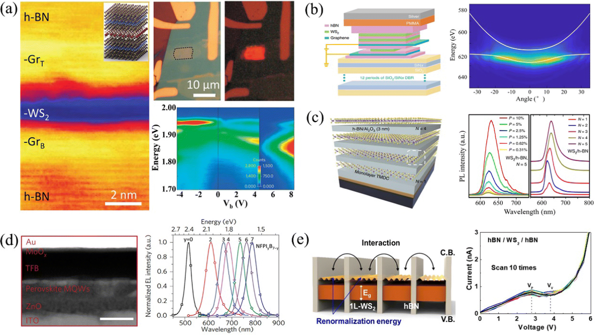 | ||
| Fig. 5 (a) TEM (left), optical and EL (top) images of a CS sample. Maps of PL and EL spectra of the related devices (down). Reproduced with permission.33 (b) Structural schematic and angle-resolved PL properties of a luminescent device integrated a h-BN/WS2 CS with a distributed Bragg reflector. Reproduced with permission.112 (c) Structure and PL characterizations of a TMD/h-BN/Al2O3 multiple QWs CS sample. Reproduced with permission.114 (d) TEM image and EL spectra of a layered perovskite-based light-emitting diode. The scale bar is 50 nm. Reproduced with permission.115 (e) Electronic band structures and NDR behaviors of a h-BN/WS2 CS device. Reproduced with permission.113 Copyright 2015, 2016, 2019, 2021, Nature Publishing Group. Copyright 2020, American Chemical Society. | ||
In addition, the above quantum tunneling of carriers between barriers can also give rise to exotic properties of materials such as the negative differential resistance (NDR) phenomenon.116 In conventional type III heterostructures, a weak electric field drives carriers tunneling from the maximum valence band (VB) of one material with lower energy to minimum conduction band (CB) of another with higher energy. But when the bands with lower energy move up under an increased field, carrier transportation will be hindered, manifested as the tunneling current of the device decreases. This downward trend does not continue until the current rises when the new bands are matched by continuous excitation of the external electric field. As a whole, the current of the device will experience a period of decline in the process of overall increase. If the heterostructure is replaced with a superlattice with multiple QWs, this NDR phenomenon can occur many times.117,118 The influence of this band alignment is more significant in CSs due to the sharper interface between layers, so a more obvious NDR behavior was predicted in 2014.119 The corresponding experimental phenomenon has also been observed by Lee et al. in WS2/h-BN CSs in 2020 (Fig. 5e).113
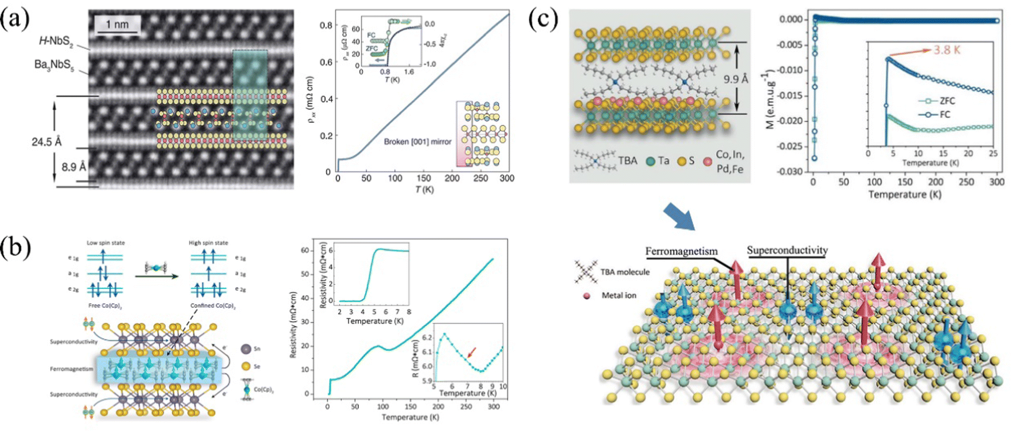 | ||
| Fig. 6 (a and b) Schematic and temperature-dependent resistivity of a H-NbS2/Ba3NbS5 (SnSe2/Co(Cp)2) superlattice. The devices exhibit the superconducting transition at temperatures below 0.8 and 4 K, respectively. Reproduced with permission.121,122 (c) Temperature-dependent resistivity of a Co-TaS2 molecular superlattice. Interestingly, the device exhibits ferromagnetism under field-cooling and zero-field-cooling processes. Reproduced with permission from.123 Copyright 2020, American Association for the Advancement of Science. Copyright 2017, American Chemical Society. Copyright 2020, Wiley-VCH. | ||
3.2 Properties and applications of SS
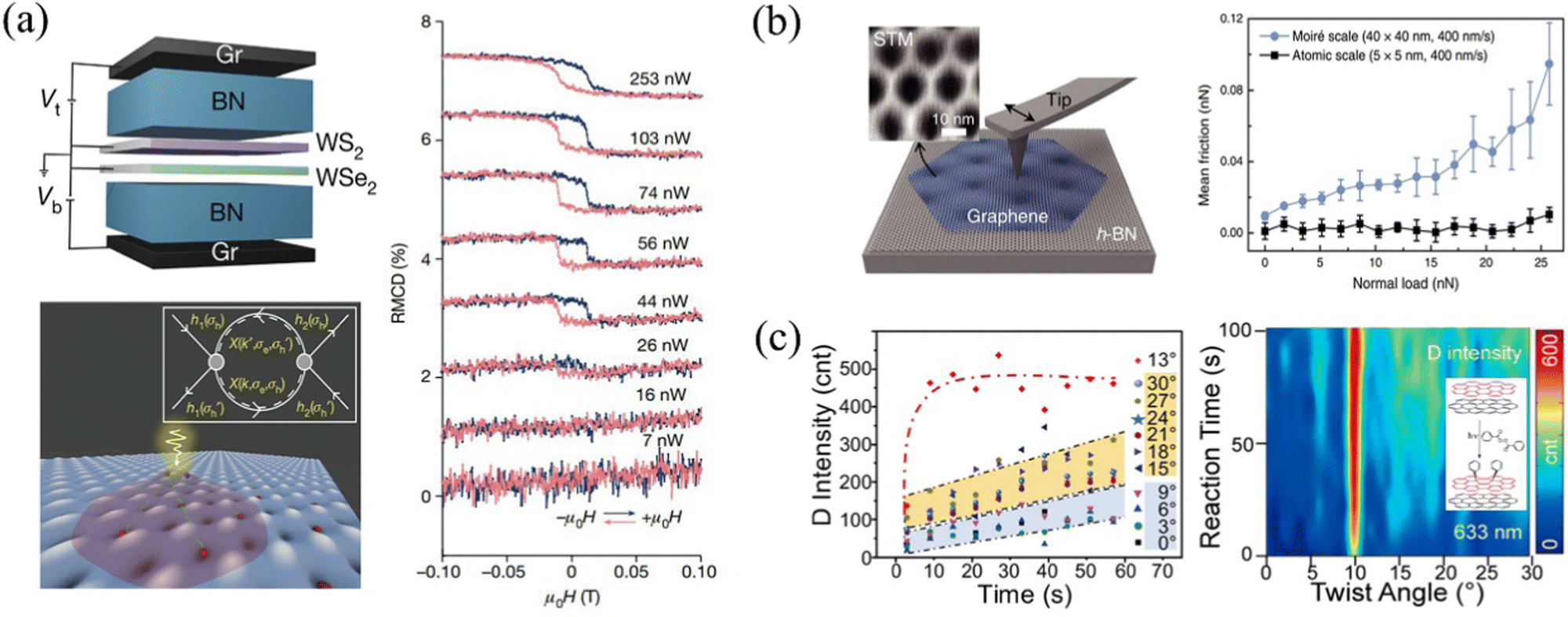
The properties of CSs, especially in the field of optoelectronics, are mainly attributed to their periodic modulation of band structures, but the complex preparation process always limits the further development. So, it is natural to think of other methods to achieve the modulation, gradually leading to other types such as SSs. 2D materials possess a high Young's modulus and usually exhibit stronger mechanical strength than their bulk materials.124 By inducing strain or other factors to change the band structures, the interfacial performance of 2D materials can be tailored effectively. When introducing the modulation periodically at the nanoscale, the carrier transportation will be greatly altered, causing behaviors like conventional superlattices.8–11,125,126 This is one of the main bases to judge whether the material studied is SS. Due to an emerging material system in almost the last 5 years, most related works are still focused on the properties exploration now.In 2017, Andrei's group reported a feasible route to introduce a pseudomagnetic field to graphene by inducing periodic strain.57 The band structure of graphene was reconstructed into pseudo-Landau levels (PLL) and a sequence of PLL peaks in the DOS were observed (Fig. 7a). The similar phenomenon was reported again in 2019.26 Interestingly, this time they presented a new way for making flat bands in another graphene SS, which is expected to be a theoretical basis for the important role of this SS in superconductivity. Almost at the same time, Banerjee et al. also reported an intense pseudogauge field generated in a graphene SS.77 The carbon–carbon bond length changed and affected Dirac electrons. The DOS fluctuates periodically with an applied bias, and the period is directly related to the spatial scale of the periodic strain in SS (Fig. 7b). In addition to the above research, the quantum confinement enhancement and periodic energy valley properties are involved recently, which also predicts the prospect of SS applied in the photovoltaic fields.127,128 In 2020, Tian's group investigated the difference of interfacial interaction between the pristine graphene and SS (Fig. 7c).129 Compared with the relatively low photocurrent value in the central region of the superlattice, the photocurrent increased significantly at the interface between original graphene and SS. By analyzing the photothermoelectric current (IPTE) formula IPTE = ΔS·ΔT/R, where ΔS, ΔT and R are respectively the Seebeck coefficient difference between the two regions, temperature difference around the light point and device resistance, they concluded that the large Seebeck coefficient shift caused by the deformation of the internal band structure plays a key role here.
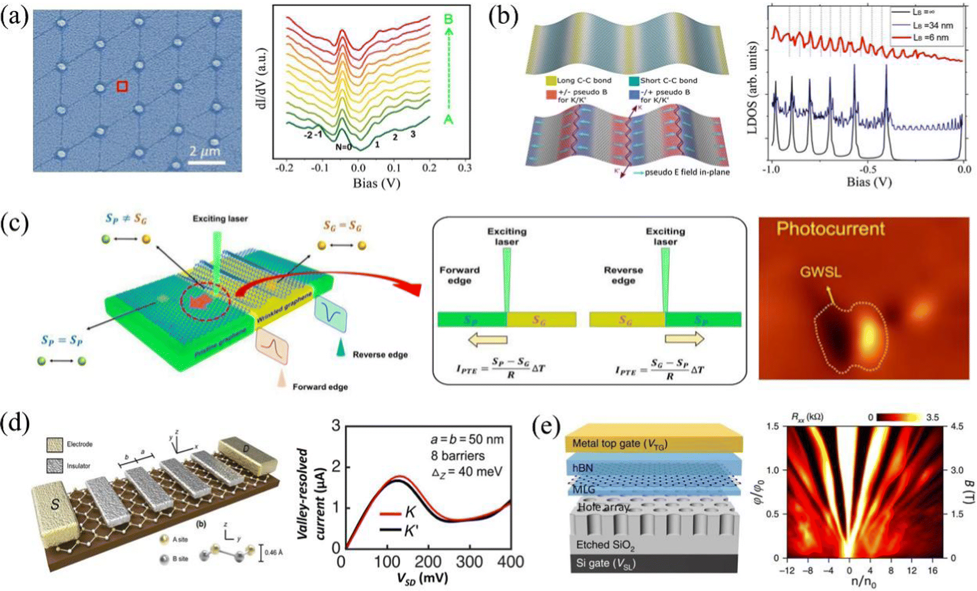 | ||
| Fig. 7 (a) Left: SEM image of a graphene/Au pillars SS sample. The periodic dots and dark lines are Au pillars and strain-induced graphene ripples, respectively. Right: Spatial-dependent dI/dV curves of the SS sample. Different from the featureless ‘V’ shape of unstrained graphene, the SS graphene sample exhibits many peaks here, indicating the presence of pseudomagnetic field. Reproduced with permission.57 (b) Pseudogauge fields and calculated DOS of a graphene SS. When the strain period applied to the material changes, the energy peak period of Landau quantization changes accordingly. Reproduced with permission.77 (c) Schematic and enhanced photocurrent of a graphene SS. The difference in Seebeck coefficients between the pristine and folded graphene enhances the photothermoelectric effect at the interface. Reproduced with permission.129 (d) Structural schematic and NDR behaviors of a silicene SS. Reproduced with permission.132 (e) Schematic and longitudinal resistances at different normalized densities and magnetic fields of a graphene/dielectric hole SS. Reproduced with permission.27 Copyright 2017, 2020, American Chemical Society. Copyright 2018, American Physical Society. Copyright 2018, Nature Publishing Group. | ||
Apart from the periodic strain, introducing the external localized fields can also modulate the performance of 2DSs.130,131 By transferring a 2D material onto a substrate with periodic nano-structures as the design, the material may behave as a superlattice. In this sense, the definition of abovementioned SS can be further extended. For example, in 2018 Chen et al. applied an out-of-plane periodic electric field on the silicene and observed the typical NDR behaviors usually presented in CSs (Fig. 7d).132 Interestingly, the devices exhibit controllable valley and spin degrees of freedom for modulation, suggesting a broader application prospect. In another work, Forsythe et al. transferred an h-BN/graphene/h-BN heterostructure onto a SiO2 substrate with periodic triangular/square nanohole arrays.27 When the material was stimulated by a magnetic field, the fractal mini-gaps of the Hofstadter spectrum were observed (Fig. 7e). The quantum Hall effect is completely caused and amplified by the band structure modification arising from the substrate. The intensity of the magnetic field that needs to be applied here is nearly an order of magnitude lower than that in most MSs.133,134 Similarly, by designing an h-BN/graphene/h-BN heterostructure etched with periodic nanoholes, Jessen et al. also modulated the band structure of graphene.28 In 2021, by placing graphene/h-BN on SiO2 nanoarray structures, Dean et al. synthesized another SS and observed the main and satellite Dirac cones later.135
In addition to the above reports that 2DSs can be achieved by an applied field, considerable recent work has focused on conducting periodic nanomachining on 2DCSs to directly regulate their properties. For example, a CS prepared with periodic stacking of graphene and dielectric films has been reported as a hyperbolic metamaterial, and it absorbs an incident electromagnetic wave perfectly in the near-infrared (NIR) band.136 By preparing a nanograting on its surface, the absorption can be further extended to the visible range. In another work, Yan et al. periodically arranged graphene with an organic buffer layer and etched it into ribbons and discs. After the treatment, the materials can modulate the plasmon in graphene and respond to polarization or strongly absorb terahertz or far-infrared waves.137 In this case, the 2DSs and metamaterials have many similarities in their properties. A clearer definition is needed in the future to distinguish between the two.
Apart from the above discussion, there are still several points to note about SSs. First, due to the high Young's modulus, the deformation of 2D materials under the action of vdW forces between the interfaces is inevitable when transferring them onto other 2D materials or substrates. Once the strain exceeds a critical value, the periodic interfacial buckling will appear and the changes in material properties cannot be ignored. This is the reason why people hope to regulate the properties of 2D materials by constructing SSs. Second, regulating the band structures of original materials for tuning their properties is still dominant in most of the existing SSs. But because the specific physical mechanisms involved are different, it is hard to describe the strain in the superlattice quantificationally. At the same time, considering the different natures of materials itself and the forms of strain, it is also difficult to establish an accurate correspondence between strain and the related properties/applications. Finally, whether the strain plays a major role in the process of material property changes needs a comprehensive consideration. Multiple forms of interactions are observed simultaneously in a certain class of superlattices, and they may work together to cause a particular property of the material. This is also one of the main reasons it is hard to quantificationally evaluate the influence of strain. However, in-depth research in this area will require a great deal of work to be done.
3.3 Properties and applications of MS
From the perspective of the development of 2DSs, the research of MSs does not show obvious lag compared with others.138 However, it is indeed the research on superconductivity and Mott-like insulating properties reported on TBG that has attracted more attention.21,22 Up to now, the components of designed MSs have been extended from different 2D materials to others such as photonic crystals.139 An emerging ‘twistronics’ involving the studies of light spin/valleytronics, localization/delocalization phenomena, topological exciton bands, etc. are developing vigorously.30–32,140–142 Since this field is in its initial development stage, most of the research on MSs is still in the performance exploration. To be different from the existing review work, here the complex theoretical descriptions are avoided and the introduction of the material properties and related practical applications are mainly focused on. | ||
| Fig. 8 (a) Schematic (left), energy band structure, DOS (middle) and temperature-dependent four-probe resistances (right) of different TBG-MS samples. Two superconducting domes are observed. Reproduced with permission.21 (b) Schematic (left), temperature-dependent resistances (middle) and resistance map (right) with different Landau fans and applied displacement fields of a TTG-MS sample. Reproduced with permission.148 (c) Schematic and rectified electrical properties of a BP orientation-dependent photodiode. Reproduced with permission.149 (d) Schematic, TEM images and temperature-dependent NDR behaviors of a trilayer orthogonal BP MS. Reproduced with permission.151 Copyright 2018, 2021, Nature Publishing Group. Copyright 2018, Wiley-VCH. Copyright 2021, American Association for the Advancement of Science. | ||
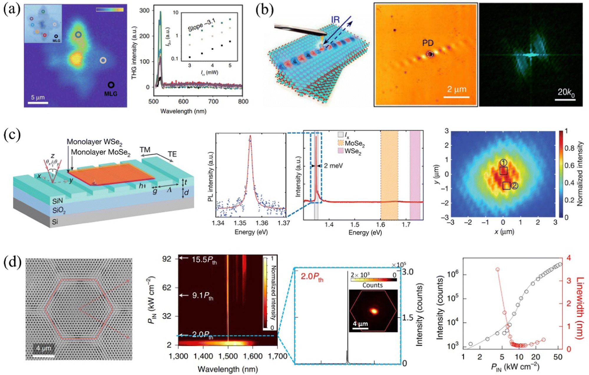
The flat band properties in TBG or TTG have promoted the rapid development of similar systems, but their practical applications in electronics are still rare.31,139 People are trying to do research from the perspectives by considering different materials and device structures. In 2018, Xin et al. fabricated the orientation-dependent diodes by observing the rectification in few-layered BP vdW MSs.149 The armchair (AC) orientation of the upper BP is vertical to the lower one (vertical-twisted BP), and maximum rectification ratio of the diode reaches 115 (Fig. 8c). In contrast, the devices made of ‘parallel-twisted BP’ show completely different linear ohmic behaviours.149,150 The anisotropic band structure of BP and the discrepant effective mass of electrons and holes are the main reasons for this phenomenon. Based on the formula  , where kB, T and m are the Boltzman's constant, kelvin temperature and effective mass of carriers respectively, the band difference (ΔE) between the armchair (AC) and zigzag (ZZ) orientations could be estimated. Similar results were also found by Lee's group in 2021, but the difference was the observation of a symmetric nonlinear voltage–current curve instead of the rectification phenomenon.151 This may be related to the oxidation protection on BP in the former experiment. By fabricating more complex BP-MS structures, Lee et al. further prepared the resonant tunnelling diode, which exhibits a typical NDR phenomenon (Fig. 8d). In order to explore the mechanism, a physical model described by two-band block Hamiltonians was established. They believed that the different crystalline orientations between adjacent BPs lead to the changes of band structures, so that the QW states originate from the electronic wavefunction confinement appeared, resulting in the resonant tunnelling behaviors similar to that in traditional superlattices. Significantly, the BP MSs here present great advantages in modulating and optimizing the performance of related devices in normal environment. This is different from the TBG systems in that their flat band properties are usually observed at low temperatures.
 | ||
| Fig. 9 (a) Left: Scanning THG image of a graphene sample with uneven thicknesses. Right: Typical THG spectra of the graphene sample at different regions excited by 520 nm laser. The TBG position can be excited by the strongest signal. Reproduced with permission.156 (b) Schematic (left), near-field amplitude distribution (middle) and its Fourier transformed dispersion curves of a twisted α-MoO3 sample. A highly oriented amplitude distribution in the middle indicates anisotropic topological polariton transportation. Reproduced with permission.160 (c) Schematic (left), PL spectrum (middle) and a typical interferograms (right) above threshold of a 0°-twisted WSe2–MoSe2 exciton laser. Reproduced with permission.170 (d) SEM image (left), normalized spectra (middle) and intensity/linewidth evolution curves of a nanostructured magic-angle laser on InGaAsP multiple QWs. A phase transition from spontaneous emission to laser above threshold can be found from the normalized spectra. Reproduced with permission.171 Copyright 2019, 2020, 2021, Nature Publishing Group. | ||
With the deepening research in recent years, the optical properties exploration of MSs has been expanded in a large range, such as in the field of optical coherent injection, chiral circular dichroism, light-induced ferromagnetism and so on.157–159 The different material systems have also attracted constant attention. For example, in 2020, Qiu's group predicted that the photonic dispersion of phonon polaritons in twisted α-MoO3 can transition topologically from hyperbolic to elliptical contours with changing the sample angle.160 Under a particular rotation (photonic MA), the dispersion flattens and causes diffractionless polariton propagation. This expectation was confirmed in the experiment afterwards and the light wavelength was compressed 40 times in this method, suggesting an important development prospect in nanoimaging or other fields (Fig. 9b). Similar results were also confirmed by Chen et al. subsequently.161
Apart from the optical research mentioned above, the PL of MSs is also an engrossing field which is closest to practical applications at present. Different from the zero bandgap of graphene material, TMDs or photonic crystals have a greater advantage in light emission due to its sizeable bandgap. In 2014, Liu et al. studied the luminescence properties of MoS2-MSs and discussed the interlayer exciton coupling by observing the variation of spectral peaks.68 Subsequently, various groups studied in detail the relationship between PL and twisted angle of different TMD-based MSs, respectively.162–164 Due to the momentum mismatches and formation of resonance hybridized excitons during rotation, the twisted angle can still lead to a huge difference in the luminescence properties even if the material remains unchanged. Although the mechanism of the TMD-based MSs is still controversial, the spin-valley locking effect and controllable moiré exciton properties in electromagnetic fields also lay a solid foundation for their practical applications.165–169 In 2019, Paik et al. integrated a WSe2–MoSe2 bilayer material with a silicon nitride grating resonator.170 By accurately matching the momentum of the TMD-MS and stimulating the interlayer excitons, they achieved a more than 100-fold increase in light emission across the lasing threshold (Fig. 9c). An extended spatial coherence length proves laser generation rather than ordinary luminescence. In 2021, Ma's group further introduced the concept of MSs into photonic crystals and fabricated the samples which contains two in-plane sets of nanohole arrays with a twisted angle in a single InGaAsP material.171 Due to the stronger field confinement, the devices made of these nanocavities can emit lasers with a narrower spectral linewidth (Fig. 9d).
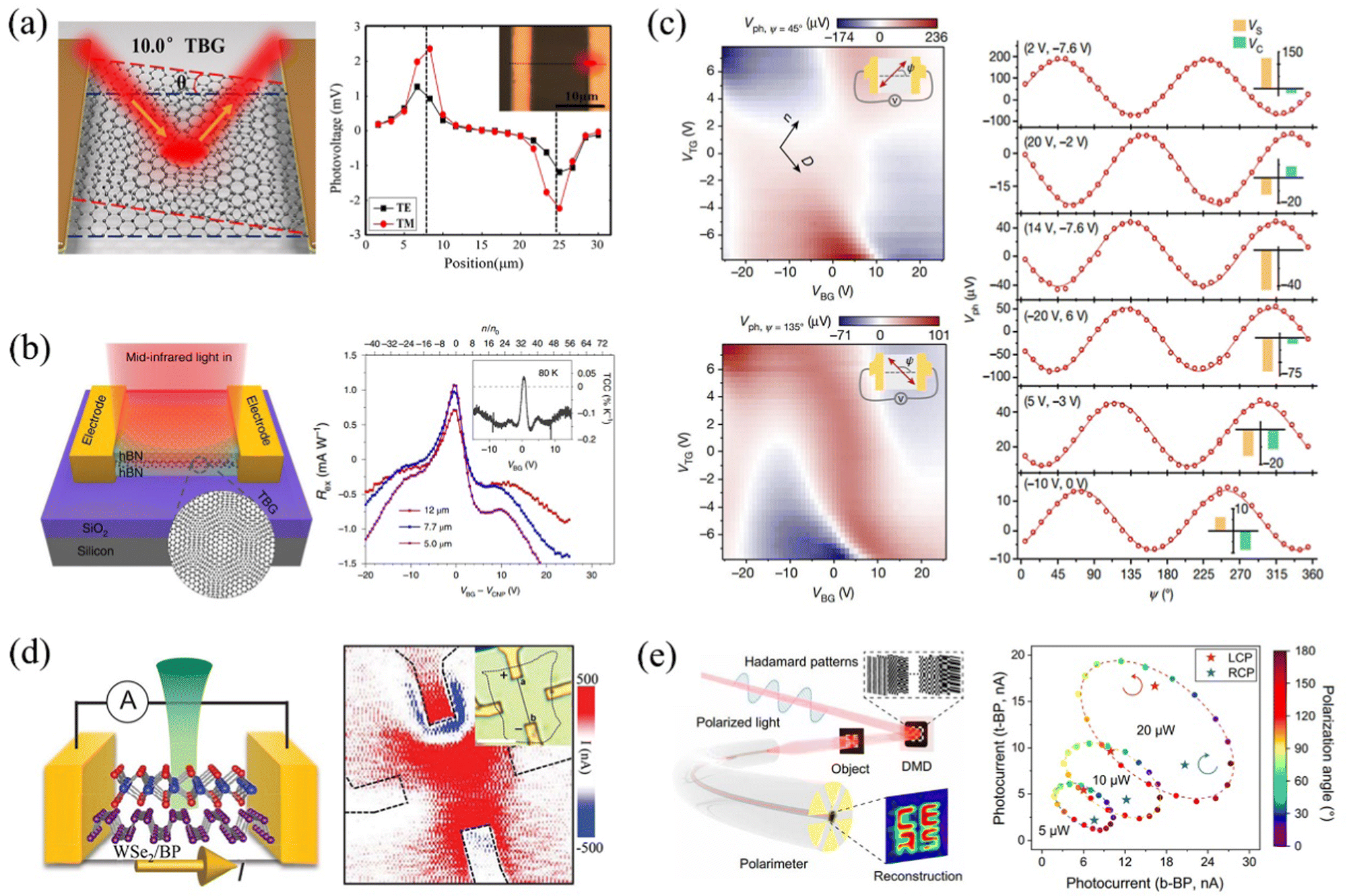 | ||
| Fig. 10 (a and b) Schematics and photoresponse measurements of TBG MSs in visible and mid-infrared bands respectively. Reproduced with permission.174,176 (c) Left: Gate-tunable linear bulk photovoltaic voltage (Vph) excited by a linearly polarized light (λ = 7.7 μm) with polarization angle ψ = 45° (top) and ψ = 135° (bottom), respectively. Right: Polarization dependence of Vph when fixing the gate voltages. Reproduced with permission.177 (d) Schematic and photocurrent mapping of a WSe2/BP photodetector excited by a linearly polarized 532 nm laser. Reproduced with permission.179 (e) Schematic and 2D polarization-dependent photocurrent of a twisted BP/BP/Bi2Se3 fiber-integrated polarimeter. Reproduced with permission.180 Copyright 2016, Wiley-VCH. Copyright 2021, 2022, American Association for the Advancement of Science. Copyright 2020, 2022, Nature Publishing Group. | ||
In addition to the graphene-based MS mentioned above, recently the MS made of other 2D materials have also attracted extensive attention in photodetection. In 2021, Akamatsu et al. designed a WSe2–BP MS and observed its spontaneous photocurrent without actuation by a bias voltage.179 Different from the traditional heterostructures, the strict crystal alignment needs to be considered. Only when the threefold rotational symmetry of WS2 is parallel to the AC direction of BP, the interesting phenomenon can occur. From the photocurrent map we can find that the photoresponse appears in the stacking area instead of the material–electrode junction (Fig. 10d). This is similar to that in the BP homostructures, and the geometrical and topological nature at the WSe2–BP interface play a key role.150 In another work, Xiong et al. integrated a few-layered Bi2Se3-BP-BP MS into the end face of a fiber to measure the intensity and polarization of incident light rigorously (Fig. 10e).180 They established the following relationship between photocurrent (I), light power (P) and polarization angle (φ):
| I = m·Pn, |
 | ||
| Fig. 11 (a) Schematics (left top) and optical-induced ferromagnetism phenomena (right) of a voltage-regulated WS2/WSe2 MS at 1.6 K. The exciton-mediated long-range spin–spin interactions play a key role here (left bottom). Reproduced with permission.159 (b) Left: STM and schematic images of a graphene/h-BN MS. Right: The corresponding unusual stick slip measurements both at the moiré and atomic scales. Reproduced with permission.188 (c) Comparison of chemical reactions between BPO and TBGs with different twisted angles through the Raman signatures. For some samples with specific angles, the reaction rate is enhanced. Reproduced with permission from.190 Copyright 2022, Nature Publishing Group. Copyright 2022, American Physical Society. Copyright 2015, American Chemical Society. | ||
In addition to the above magnetic novelty, MSs also present outstanding performance in mechanics and thermodynamics.186 For example, by studying the tribological properties of h-BN/graphene MSs, Zheng's group found that lattice mismatch can lead to microscale structural superlubricity at the interface.187 The friction changes little even in rotation of the dislocation contact and the shear stress here is about orders of magnitude lower than that in homogeneous junctions. The smooth soliton-like motion of the moiré pattern ridges was demonstrated crucial through the kinetic simulations. Not long ago, Zhang et al. also studied the stick slip behaviors of the same material system in detail.188 The stick slip manifests at both the atomic and moiré scales when a nanoscale tip is slid on the h-BN/graphene MS surface (Fig. 11b). Interestingly, because the structural lubricity of the material is closely related to its thermal characteristic, the h-BN/graphene MS also provides an excellent platform for its thermodynamic study. In 2021, Ren et al. studied the interfacial thermal transport of this system as the twisted angle changed. This rotation caused the surface undulations between layers, enhancing the interfacial phonon scattering and influencing the thermal conductance accordingly.189
Besides, the interlayer coupling of carriers MSs also greatly affects the chemical reaction rate of materials. Taking the TBG material as an example, especially when the incident light energy matches well with the interval between VHSs, the chemical reactivity of graphene material will be greatly enhanced. Based on this, in 2015, Liu's group investigated the chemical reaction between TBG and benzoyl peroxide (BPO) systematically.190 The TBG with 13° twisted angle has been shown faster chemical reaction rate (Fig. 11c). A similar phenomenon in the reactions of TBG with diazonium salts was also observed soon after by Luo's group.191 According to the Gerischer–Marcus electron transfer theory analysis and electronic structure calculations, they believed that the variant distribution of DOS in energy gap leads to different reactivities. In 2018, the chemical reaction research of MSs is further extended to TTG materials.192 The 30°–30° TTG displayed the highest phenyl radical grafting speed.
4. Opportunities and challenges
The appearance of 2DSs provides a platform for expanding the properties and applications of 2D materials, such as in the field of electronics or optoelectronics. Although this concept is drawn from earlier knowledge of conventional semiconductors, the atomic lattices and unique properties of 2D materials bring new opportunities for their development. In particular, when the introduction of interfacial moiré properties brings spintronics and twistronics into public horizon, 2DSs cannot be regarded as a brief imitation and expansion of traditional materials and structures. Table 1 summarizes the application status of 2DSs in different fields. Most of the work (∼70%) took place within the last five years, indicating an emerging attractive field and broad prospects in the further.193–202| Applications | Type | Materials | Symbolic parameters | Ref. | Year |
|---|---|---|---|---|---|
| Energy storage | CS | LDH/rGO | Capacity up to 650 F g−1 | 40 | 2014 |
| CS | Ni-Al LDH/rGO | 72.7% initial capacitance maintains after 10![[thin space (1/6-em)]](https://www.rsc.org/images/entities/char_2009.gif) 000 cycles 000 cycles |
95 | 2016 | |
| CS | MoS2/graphene | Anode delivered specific capacity of 240 mA h g−1 at 51.2 A g−1 and more than 380 mA h g−1 at 10 A g−1 over 1000 cycles, onset potential of 88 mV, Tafel slope of 48.7 mV decade−1 | 96 | 2018 | |
| CS | Fe-N-C/MXene | A positive onset potential of 0.92 V, strong durability of 20 h | 97 | 2020 | |
| CS | Co-Al LDH-NS/GO | Long cyclic life, specific capacitance up to 1204 F g−1 under 5 mV s−1 | 99 | 2012 | |
| CS | β-Ni(OH)2/graphene | Highest specific capacitance of 660.8 F cm−3 | 100 | 2013 | |
| CS | Ti3C2/Ni-Co-Al-LDH | Specific capacitance of 748.2 F g−1 at 1 A g−1, maximum energy density of 45.8 W h kg−1 as positive electrode | 101 | 2017 | |
| CS | SnO/pristine graphene | Reversible capacity of 633.9 mA h g−1 at 0.05 A g−1, 700 cycles at 1 A g−1 | 107 | 2020 | |
| CS | CoFe-LDH/NiFe-LDH | A voltage of 1.59 V at 10 mA cm−2 | 109 | 2019 | |
| SS | VOPO4-graphene | Specific capacity of 160 mA h g−1, energy density of ∼570 W h kg−1 | 102 | 2020 | |
| SS | WS2 wrinkle arrays | An overpotential of 121 mV versus reversible hydrogen electrode | 198 | 2021 | |
| MS | WS2 | An overpotential of 60 mV at 10 mA cm−2, Tafel slope of 40 mV decade−1 | 194 | 2021 | |
| MS | MoS2 | An overpotential of −153 mV at −10 mV cm−2, Tafel slope of 73 mV decade−1 | 195 | 2019 | |
| Superconductivity | CS | Ba3NbS5/H-NbS2 | A BKT transition at ∼0.82 K | 121 | 2020 |
| CS | TaS2 | A superconductivity transition at ∼3.8 K | 123 | 2020 | |
| MS | TBG (1.1° ± 0.1°) | A superconductivity transition at ∼1.7 K | 21 | 2018 | |
| MS | TBG (0.93° ± 0.01°) | A superconductivity transition at ∼0.3 K | 144 | 2019 | |
| MS | TTG (∼1.56°) | A superconductivity transition at ∼2.1 K | 148 | 2021 | |
| MS | TBG (> 1.1°) | Largest superconductivity transition temperature is ∼3 K with pressure | 196 | 2019 | |
| NDR properties | CS | WSe2/SnSe2 | Peak-to-valley current ratio (PVCR) of 1.8 at 300 K, PVCR of 2.8 at 80 K | 116 | 2021 |
| CS | MoTe2/hexacarbonitrile | PVCR of maximum ∼137 | 199 | 2021 | |
| SS | Silicene | PVCR of 4.7 under a low operating bias at room temperature | 132 | 2018 | |
| MS | BP | PVCR of 3 at 300 K, PVCR of ∼9 at 4.8 K | 151 | 2021 | |
| Photo absorption | CS | rGO/PDDA | Broadband absorption of >80% of unpolarized light from 300 to 2500 nm | 136 | 2019 |
| SS | BP | Absorption band edge shift of up to ∼0.7 eV | 127 | 2016 | |
| SS | MoS2 | Enhanced broadband absorption from 677 to 905 nm | 201 | 2015 | |
| MS | TBG (10°/13°) | ∼3 times the photo absorption of ordinary monolayer graphene | 153 | 2016 | |
| MS | Perovskite (30°) | 28.5% enhancement of light harvesting | 173 | 2021 | |
| Photodetection | SS | BP | Peak detectivity of 5.97 × 10⁹ Jones at λ = 4.0 μm (0.4%; compressive), 8.45 × 10⁹ Jones at λ = 2.0 μm (1.0%; tensile) | 126 | 2021 |
| SS | Graphene wrinkle | Photoresponsivity of 1.8 × 10⁻⁴ A W−1 (> 15 times higher than pristine graphene) | 129 | 2020 | |
| MS | TBG | Maximum photoresponsivity of ∼1 mA W−1 of 13.0° TBG at λ = 532 nm | 72 | 2016 | |
| MS | TBG | Photoresponsivity of ∼9 mA W−1 of 10.0° TBG at λ = 633 nm | 153 | 2016 | |
| MS | TBG | Photovoltage of 1.2–2.2 mV of 10.0° TBG, 0.88–1.62 mV of 12.0° TBG | 174 | 2016 | |
| MS | Graphene/h-BN | A zero-bias photoresponsivity of 0.3 A W−1 at λ = 660 nm | 175 | 2016 | |
| MS | TBG | Photoresponsivity of 26 mA W−1 of 1.81° TBG at λ = 12 μm | 176 | 2020 | |
| MS | TBG | Response time around 4 ns, response ranges from visible to THz | 178 | 2020 | |
| Luminescence | CS | Graphene/TMDs/h-BN | Quantum efficiency of ∼8% | 33 | 2015 |
| CS | h-BN/WS2 | EQE up to ∼0.1% | 112 | 2019 | |
| CS | TMD/h-BN/Al2O3 | >90% narrow band absorption, Rabi splitting of up to 170 meV | 114 | 2022 | |
| CS | Perovskite | EQE up to 11.7%, energy conversion efficiency of 5.5% at 100 mA cm−2 | 115 | 2016 | |
| CS | InAs/GaSb | MWIR LED: 6.7 W cm−2 sr−1 | 193 | 2017 | |
| SS | MoS2 | PL emission is quenched >50% with respect to that at unstrained interfaces | 125 | 2019 | |
| MS | MoSe2/WS2 | Tunable PL peaks around ∼0.1 eV | 164 | 2019 | |
| MS | WSe2–MoSe2 (0°) | 100-fold intensity enhancement of emission, spectrum width of 2 meV, 2000 of Q-factor | 170 | 2019 | |
| MS | Photonic crystal | Bandwidth of ∼0.000091 nm, lasing threshold of ∼6 kW cm−2 | 171 | 2021 | |
| MS | TBG (17.5°) | 5-Time enhancement in PL | 197 | 2019 | |
| Topological properties | SS | Graphene wrinkle | A modulated short-range (∼1–10 nm) pseudo-gauge field (∼100 T) | 77 | 2021 |
| SS | Graphene/h-BN | Pseudo-magnetic fields up to ∼800 T | 202 | 2020 | |
| MS | h-BN | Ferroelectric with oppositely polarized dipoles | 200 | 2021 |
However, this field is still far from developed and it faces many challenges for development. To simply judge the current status and future trend, we evaluate different 2DSs from six aspects (Fig. 12). Two main issues are primarily believed to be addressed after in-depth analysis. First, high-quality, wafer-scale and convenient preparation of 2DSs is a basic for further development. This is consistent with the current problems faced by the preparation of 2D materials and their heterostructures, while the more complex architectures of 2DSs face more serious requirements. Taking the MS as an example, its properties are directly impacted by the material type, stacking order, twisted angle, interfacial coupling and other factors. Preparing an MS sample design is undoubtedly full of challenges if all the above factors are taken into account. Similarly, when preparing CSs, the preparation efficiency and alternative material types need to be considered; the fabrication accuracy of micro/nanostructures and compatibility with 2D materials should be concerned in SSs preparation. In general, self-assembly technique has great potential due to the rapid and high-quality preparation of materials, and the integration of multiple preparation technologies will be the trend for development.203–206
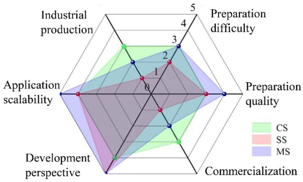 | ||
| Fig. 12 Comparison diagram of different 2DSs in full scales. For each aspect, we will evaluate it on a scale of 1 to 5. | ||
Second, theoretical prediction, including the construction of physical model and simplified calculation, of 2DSs’ properties is another key to promote the development. The initial research on the properties of CSs is indeed based on the expansion of traditional knowledge, but the new forms of 2DSs also bring much unpredictability to novel phenomena. For example, the research on luminescence performance of CSs in recent years is still a recurrence of multiple QW model. It is not completely reasonable to only consider the influence of band offsets but ignore other factors such as the moiré potential, correlated states, chirality and topology in materials. There are no strict structural boundaries for different 2DSs in principle, but it is necessary to open up new paths to comprehensively consider the above factors and obtain predicted results quickly. The theoretical simulation that relies on traditional first-principles calculation will face great computational pressure.177,207
In conclusion, this review introduces the common 2DSs from an overall perspective. We reorganize the existing classifications, and mainly focus on the preparation methods, properties and applications. If the 2DSs are applied practically, how to realize their industrial preparation and predict their properties conveniently are two key problems. Although many challenges exist, such new conceptional materials are still attractive because of the more versatile manipulation of material properties. It can be predicted that the related research in theory and experiment will develop in more diversified 2DSs.
Conflicts of interest
The authors declare no conflict of interest.Acknowledgements
The authors acknowledge financial support from the Foundation of Jilin Educational Committee (JJKH20221151KJ), the National Natural Science Foundation of China (12274065 and 11804334), and the Fundamental Research Funds for the Central Universities (2412021QD004).Notes and references
- L. Esaki and R. Tsu, IBM J. Res. Dev., 1970, 14, 61 CAS.
- L. Esaki and L. Chang, Phys. Rev. Lett., 1974, 33, 495 CrossRef CAS.
- F. F. So and S. R. Forrest, Phys. Rev. Lett., 1991, 66, 2649 CrossRef CAS PubMed.
- G. A. Sai-Halasz, R. Tsu and L. Esaki, Appl. Phys. Lett., 1977, 30, 651 CrossRef CAS.
- L. W. Whitlow and T. Hirano, J. Appl. Phys., 1995, 78, 5460 CrossRef CAS.
- G. Rijnders and D. H. A. Blank, Nature, 2005, 433, 369–370 CrossRef CAS PubMed.
- T. C. Harman, P. J. Taylor, M. P. Walsh and B. E. LaForge, Science, 2002, 297, 2229–2232 CrossRef CAS.
- R. Ramesh and D. G. Schlom, Nat. Rev. Mater., 2019, 4, 257–268 CrossRef.
- P. Chen, Z. Zhang, X. Duan and X. Duan, Chem. Soc. Rev., 2018, 47, 3129–3151 RSC.
- Y. Huang, J. Liang, C. Wang, S. Yin, W. Fu, H. Zhu and C. Wan, Chem. Soc. Rev., 2020, 49, 6866–6883 RSC.
- Y. K. Ryu, R. Frisenda and A. Castellanos-Gomez, Chem. Commun., 2019, 55, 11498–11510 RSC.
- K. S. Novoselov, A. K. Geim, S. V. Morozov, D. Jiang, Y. Zhang, S. V. Dubonos, I. V. Grigorieva and A. A. Firsov, Science, 2004, 306, 666–669 CrossRef CAS PubMed.
- C. Chang, W. Chen, Y. Chen, Y. Chen, Y. Chen, F. Ding, C. Fan, H. Fan, Z. Fan, C. Gong, Y. Gong, Q. He, X. Hong, S. Hu, W. Hu, W. Huang, Y. Huang, W. Ji, D. Li, L. J. Li, Q. Li, L. Lin, C. Ling, M. Liu, N. Liu, Z. Liu, K. P. Loh, J. Ma, F. Miao, H. Peng, M. Shao, L. Song, S. Su, S. Sun, C. Tan, Z. Tang, D. Wang, H. Wang, J. Wang, X. Wang, X. Wang, A. T. S. Wee, Z. Wei, Y. Wu, Z. S. Wu, J. Xiong, Q. Xiong, W. Xu, P. Yin, H. Zeng, Z. Zeng, T. Zhai, H. Zhang, H. Zhang, Q. Zhang, T. Zhang, X. Zhang, L. D. Zhao, M. Zhao, W. Zhao, Y. Zhao, K. G. Zhou, X. Zhou, Y. Zhou, H. Zhu, H. Zhang and Z. Liu, Acta Phys. Chim. Sin., 2021, 37, 2108017 Search PubMed.
- K. Khan, A. K. Tareen, M. Aslam, R. Wang, Y. Zhang, A. Mahmood, Z. Ouyang, H. Zhang and Z. Guo, J. Mater. Chem. C, 2020, 8, 387–440 RSC.
- C. Liu, H. Chen, S. Wang, Q. Liu, Y. G. Jiang, D. W. Zhang, M. Liu and P. Zhou, Nat. Nanotechnol., 2020, 15, 545–557 CrossRef CAS PubMed.
- Y. Liu, N. O. Weiss, X. Duan, H. C. Cheng, Y. Huang and X. Duan, Nat. Rev. Mater., 2016, 1, 16042 CrossRef CAS.
- Y. Liu, Y. Huang and X. Duan, Nature, 2019, 567, 323–333 CrossRef CAS.
- A. K. Geim and I. V. Grigorieva, Nature, 2013, 499, 419–425 CrossRef CAS PubMed.
- C. Wang, Q. He, U. Halim, Y. Liu, E. Zhu, Z. Lin, H. Xiao, X. Duan, Z. Feng, R. Cheng, N. O. Weiss, G. Ye, Y. C. Huang, H. Wu, H. C. Cheng, I. Shakir, L. Liao, X. Chen, W. A. Goddard III, Y. Huang and X. Duan, Nature, 2018, 555, 231–236 CrossRef CAS.
- S. Xie, L. Tu, Y. Han, L. Huang, K. Kang, K. U. Lao, P. Poddar, C. Park, D. A. Muller, R. A. DiStasio Jr and J. Park, Science, 2018, 359, 1131–1136 CrossRef CAS PubMed.
- Y. Cao, V. Fatemi, S. Fang, K. Watanabe, T. Taniguchi, E. Kaxiras and P. Jarillo-Herrero, Nature, 2018, 556, 43–50 CrossRef CAS.
- Y. Cao, V. Fatemi, A. Demir, S. Fang, S. L. Tomarken, J. Y. Luo, J. D. Sanchez-Yamagishi, K. Watanabe, T. Taniguchi, E. Kaxiras, R. C. Ashoori and P. Jarillo-Herrero, Nature, 2018, 556, 80–84 CrossRef CAS.
- J. Wang, M. Wang, F. Xu, B. Liu, J. Lang, N. Zhang, X. Kang, Z. Qin, X. Yang, X. Wang, W. Ge and B. Shen, Light: Sci. Appl., 2022, 11, 71 CrossRef CAS PubMed.
- G. C. Osbourn, J. Appl. Phys., 1982, 53(3), 1586 CrossRef CAS.
- S. Cai, D. Breid, A. J. Crosby, Z. Suo and J. W. Hutchinson, J. Mech. Phys. Solids, 2011, 59, 1094–1114 CrossRef.
- J. Mao, S. P. Milovanović, M. Anđelković, X. Lai, Y. Cao, K. Watanabe, T. Taniguchi, L. Covaci, F. M. Peeters, A. K. Geim, Y. Jiang and E. Y. Andrei, Nature, 2020, 584, 215 CrossRef CAS PubMed.
- C. Forsythe, X. Zhou, K. Watanabe, T. Taniguchi, A. Pasupathy, P. Moon, M. Koshino, P. Kim and C. R. Dean, Nat. Nanotechnol., 2018, 13, 566 CrossRef CAS PubMed.
- B. S. Jessen, L. Gammelgaard, M. R. Thomsen, D. M. A. Mackenzie, J. D. Thomsen, J. M. Caridad, E. Duegaard, K. Watanabe, T. Taniguchi, T. J. Booth, T. G. Pedersen, A. P. Jauho and P. Bøggild, Nat. Nanotechnol., 2019, 14, 340–346 CrossRef CAS.
- R. Bistritzer and A. H. MacDonald, Proc. Natl. Acad. Sci. U. S. A., 2011, 108, 12233 CrossRef CAS.
- E. Y. Andrei and A. H. MacDonald, Nat. Mater., 2020, 19, 1265–1275 CrossRef CAS PubMed.
- D. Huang, J. Choi, C. K. Shih and X. Li, Nat. Nanotechnol., 2022, 17, 227–238 CrossRef CAS PubMed.
- X. G. Gao, X. K. Li, W. Xin, X. D. Chen, Z. B. Liu and J. G. Tian, Nanophotonics, 2020, 9, 1717 CrossRef CAS.
- F. Withers, D. Pozo-Zamudio, A. Mishchenko, A. Rooney, A. Gholinia, K. Watanabe, T. Taniguchi, S. J. Haigh, A. Geim, A. Tartakovskii and K. S. Novoselov, Nat. Mater., 2015, 14, 301 CrossRef CAS PubMed.
- G. Prando, Nat. Nanotechnol., 2017, 12, 191 CrossRef CAS PubMed.
- Y. Niu, J. Villalva, R. Frisenda, G. Sanchez-Santolino, L. Ruiz-González, E. M. Pérez, M. García-Hernández, E. Burzurí and A. Castellanos-Gomez, 2D Mater., 2019, 6, 035023 CrossRef CAS.
- H. W. Guo, Z. Hu, Z. B. Liu and J. G. Tian, Adv. Funct. Mater., 2021, 31, 2007810 CrossRef CAS.
- L. Li, R. Ma, Y. Ebina, K. Fukuda, K. Takada and T. Sasaki, J. Am. Chem. Soc., 2007, 129, 8000–8007 CrossRef CAS PubMed.
- G. Li, A. Luican, J. M. B. Lopes dos Santos, A. H. Castro Neto, A. Reina, J. Kong and E. Y. Andrei, Nat. Phys., 2010, 6, 109–113 Search PubMed.
- S. J. Haigh, A. Gholinia, R. Jalil, S. Romani, L. Britnell, D. C. Elias, K. S. Novoselov, L. A. Ponomarenko, A. K. Geim and R. Gorbachev, Nat. Mater., 2012, 11, 764–767 CrossRef CAS.
- R. Ma, X. Liu, J. Liang, Y. Bando and T. Sasaki, Adv. Mater., 2014, 26, 4173–4178 CrossRef CAS.
- B. W. Li, M. Osada, Y. Ebina, S. Ueda and T. Sasaki, J. Am. Chem. Soc., 2016, 138, 7621–7625 CrossRef CAS.
- Z. Zhang, P. Chen, X. Duan, K. Zang, J. Luo and X. Duan, Science, 2017, 357, 788–792 CrossRef CAS PubMed.
- Y. Dai, X. Ren, J. Zhang, J. Liu, H. Liu, W. Ho, X. Dai, C. Jin and M. Xie, ACS Appl. Mater. Interfaces, 2019, 11, 43766–43773 CrossRef CAS PubMed.
- P. Xiong, X. Zhang, H. Wan, S. Wang, Y. Zhao, J. Zhang, D. Zhou, W. Gao, R. Ma, T. Sasaki and G. Wang, Nano Lett., 2019, 19, 4518–4526 CrossRef CAS PubMed.
- Y. Guo, Q. Chen, A. Nie, H. Yang, W. Wang, J. Su, S. Wang, Y. Liu, S. Wang, H. Li, Z. Liu and T. Zhai, ACS Nano, 2020, 14, 1635–1644 CrossRef CAS.
- M. Liu, K. Hisama, Y. Zheng, M. Maruyama, S. Seo, A. Anisimov, T. Inoue, E. I. Kauppinen, S. Okada, S. Chiashi, R. Xiang and S. Maruyama, ACS Nano, 2021, 15, 8418–8426 CrossRef CAS.
- B. Zhao, Z. Wan, Y. Liu, J. Xu, X. Yang, D. Shen, Z. Zhang, C. Guo, Q. Qian, J. Li, R. Wu, Z. Lin, X. Yan, B. Li, Z. Zhang, H. Ma, B. Li, X. Chen, Y. Qiao, I. Shakir, Z. Almutairi, F. Wei, Y. Zhang, X. Pan, Y. Huang, Y. Ping, X. Duan and X. Duan, Nature, 2021, 591, 385–390 CrossRef CAS PubMed.
- Z. Lin, Z. Wan, F. Song, B. Huang, C. Jia, Q. Qian, J. S. Kang, Y. Wu, X. Yan, L. Peng, C. Wan, J. Zhou, Z. Sofer, I. Shakir, Z. Almutairi, S. Tolbert, X. Pan, Y. Hu, Y. Huang and X. Duan, Chem, 2021, 7, 1887–1902 CAS.
- Y. Deng, X. Xi, Y. Xia, Y. Cao, S. Xue, S. Wan, A. Dong and D. Yang, Adv. Mater., 2022, 34, 2109145 CrossRef CAS PubMed.
- X. Wang, Y. Zhao, X. Kong, Q. Zhang, H. K. Ng, S. X. Lim, Y. Zheng, X. Wu, K. Watanabe, Q. H. Xu, T. Taniguchi, G. Eda, K. E. J. Goh, S. Jin, K. P. Loh, F. Ding, W. Sun and C. H. Sow, ACS Nano, 2022, 16, 8172–8180 CrossRef CAS PubMed.
- V. Nicolosi, M. Chhowalla, M. G. Kanatzidis, M. S. Strano and J. N. Coleman, Science, 2013, 340, 1226419 CrossRef.
- S. B. Desai, S. R. Madhvapathy, M. Amani, D. Kiriya, M. Hettick, M. Tosun, Y. Zhou, M. Dubey, J. W. Ager III, D. Chrzan and A. Javey, Adv. Mater., 2016, 28, 4053–4058 CrossRef CAS PubMed.
- F. Liu, W. Wu, Y. Bai, S. H. Chae, Q. Li, J. Wang, J. Hone and X. Y. Zhu, Science, 2020, 367, 903–906 CrossRef CAS PubMed.
- Y. Huang, Y. H. Pan, R. Yang, L. H. Bao, L. Meng, H. L. Luo, Y. Q. Cai, G. D. Liu, W. J. Zhao, Z. Zhou, L. M. Wu, Z. L. Zhu, M. Huang, L. W. Liu, L. Liu, P. Cheng, K. H. Wu, S. B. Tian, C. Z. Gu, Y. G. Shi, Y. F. Guo, Z. G. Cheng, J. P. Hu, L. Zhao, G. H. Yang, E. Sutter, P. Sutter, Y. L. Wang, W. Ji, X. J. Zhou and H. J. Gao, Nat. Commun., 2020, 11, 1 CrossRef.
- G. Liu, Z. Tian, Z. Yang, Z. Xue, M. Zhang, X. Hu, Y. Wang, Y. Yang, P. K. Chu, Y. Mei, L. Liao, W. Hu and Z. Di, Nat. Electron., 2022, 5, 275–280 CrossRef CAS.
- C. R. Dean, A. F. Young, I. Meric, C. Lee, L. Wang, S. Sorgenfrei, K. Watanabe, T. Taniguchi, P. Kim, K. L. Shepard and J. Hone, Nat. Nanotechnol., 2010, 5, 722–726 CrossRef CAS PubMed.
- Y. Jiang, J. Mao, J. Duan, X. Lai, K. Watanabe, T. Taniguchi and E. Y. Andrei, Nano Lett., 2017, 17, 2839 CrossRef CAS.
- H. Kum, D. Lee, W. Kong, H. Kim, Y. Park, Y. Kim, Y. Baek, S. H. Bae, K. Lee and J. Kim, Nat. Electron., 2019, 2, 439–450 CrossRef CAS.
- X. Ma, Q. Liu, D. Xu, Y. Zhu, S. Kim, Y. Cui, L. Zhong and M. Liu, Nano Lett., 2017, 17, 6961–6967 CrossRef CAS PubMed.
- M. Liao, Z. Wei, L. Du, Q. Wang, J. Tang, H. Yu, F. Wu, J. Zhao, X. Xu, B. Han, K. Liu, P. Gao, T. Polcar, Z. Sun, D. Shi, R. Yang and G. Zhang, Nat. Commun., 2020, 11, 1 CrossRef.
- W. S. Leong, H. Wang, J. Yeo, F. J. Martin-Martinez, A. Zubair, P. C. Shen, Y. Mao, T. Palacios, M. J. Buehler, J. Y. Hong and J. Kong, Nat. Commun., 2019, 10, 1 CrossRef.
- Q. Tao, R. Wu, Q. Li, L. Kong, Y. Chen, J. Jiang, Z. Lu, B. Li, W. Li, Z. Li, L. Liu, X. Duan, L. Liao and Y. Liu, Nat. Commun., 2021, 12, 1 CrossRef PubMed.
- L. Gao, G. X. Ni, Y. Liu, B. Liu, A. H. Castro Neto and K. P. Loh, Nature, 2014, 505, 190–194 CrossRef CAS.
- S. J. Yang, J. H. Jung, E. Lee, E. Han, M. Y. Choi, D. Jung, S. Choi, J. H. Park, D. Oh, S. Noh, K. J. Kim, P. Y. Huang, C. C. Hwang and C. J. Kim, Nano Lett., 2022, 22, 1518–1524 CrossRef CAS PubMed.
- X. Zhou and G. Yu, ACS Nano, 2021, 15, 11040–11065 CrossRef CAS PubMed.
- J. Li, J. Liang, X. Yang, X. Li, B. Zhao, B. Li and X. Duan, Small, 2022, 2107059 CrossRef CAS.
- J. Zhou, J. Lin, X. Huang, Y. Zhou, Y. Chen, J. Xia, H. Wang, Y. Xie, H. Yu, J. Lei, D. Wu, F. Liu, Q. Fu, Q. Zeng, C. H. Hsu, C. Yang, L. Lu, T. Yu, Z. Shen, H. Lin, B. I. Yakobson, Q. Liu, K. Suenaga, G. Liu and Z. Liu, Nature, 2018, 556, 355–359 CrossRef CAS PubMed.
- M. Y. Li, Y. Shi, C. C. Cheng, L. S. Lu, Y. C. Lin, H. L. Tang, M. L. Tsai, C. W. Chu, K. H. Wei, J. H. He, W. H. Chang, K. Suenaga and L. J. Li, Science, 2015, 349, 524–528 CrossRef CAS.
- K. Liu, L. Zhang, T. Cao, C. Jin, D. Qiu, Q. Zhou, A. Zettl, P. Yang, S. G. Louie and F. Wang, Nat. Commun., 2014, 5, 1 Search PubMed.
- C. C. Lu, Y. C. Lin, Z. Liu, C. H. Yeh, K. Suenaga and P. W. Chiu, ACS Nano, 2013, 7, 2587–2594 CrossRef CAS PubMed.
- Z. Tan, J. Yin, C. Chen, H. Wang, L. Lin, L. Sun, J. Wu, X. Sun, H. Yang, Y. Chen, H. Peng and Z. Liu, ACS Nano, 2016, 10, 6725–6730 CrossRef CAS.
- J. Yin, H. Wang, H. Peng, Z. Tan, L. Liao, L. Lin, X. Sun, A. L. Koh, Y. Chen, H. Peng and Z. Liu, Nat. Commun., 2016, 7, 1 Search PubMed.
- L. Sun, Z. Wang, Y. Wang, L. Zhao, Y. Li, B. Chen, S. Huang, S. Zhang, W. Wang, D. Pei, H. Fang, S. Zhong, H. Liu, J. Zhang, L. Tong, Y. Chen, Z. Li, M. H. Rümmeli, K. S. Novoselov, H. Peng, L. Lin and Z. Liu, Nat. Commun., 2021, 12, 1 CrossRef.
- G. Jin, C. S. Lee, O. F. Okello, S. H. Lee, M. Y. Park, S. Cha, S. Y. Seo, G. Moon, S. Y. Min, D. H. Yang, C. Han, H. Ahn, J. Lee, H. Choi, J. Kim, S. Y. Choi and M. H. Jo, Nat. Nanotechnol., 2021, 16, 1092–1098 CrossRef CAS PubMed.
- R. Xiang, T. Inoue, Y. Zheng, A. Kumamoto, Y. Qian, Y. Sato, M. Liu, D. Tang, D. Gokhale, J. Guo, K. Hisama, S. Yotsumoto, T. Ogamoto, H. Arai, Y. Kobayashi, H. Zhang, B. Hou, A. Anismov, M. Maruyama, Y. Miyata, S. Okada, S. Chiashi, Y. Li, J. Kong, E. I. Kauppinen, Y. Ikuhara, K. Suenaga and S. Maruyama, Science, 2020, 367, 537–542 CrossRef CAS.
- E. Shi, B. Yuan, S. B. Shiring, Y. Gao, Y. Guo, Akriti, C. Su, M. Lai, P. Yang, J. Kong, B. M. Savoie, Y. Yu and L. Dou, Nature, 2020, 580, 614–620 CrossRef CAS PubMed.
- R. Banerjee, V. H. Nguyen, T. Granzier-Nakajima, L. Pabbi, A. Lherbier, A. R. Binion, J. C. Charlier, M. Terrones and E. W. Hudson, Nano Lett., 2020, 20, 3113 CrossRef CAS PubMed.
- C. Berger, Z. Song, T. Li, X. Li, A. Y. Ogbazghi, R. Feng, Z. Dai, A. N. Marchenkov, E. H. Conrad, P. N. First and W. A. de. Heer, J. Phys. Chem. B, 2004, 108, 19912–19916 CrossRef CAS.
- K. V. Emtsev, A. Bostwick, K. Horn, J. Jobst, G. L. Kellogg, L. Ley, J. L. McChesney, T. Ohta, S. A. Reshanov, J. Röhrl, E. Rotenberg, A. K. Schmid, D. Waldmann, H. B. Weber and T. Seyller, Nat. Mater., 2009, 8, 203–207 CrossRef CAS PubMed.
- A. Davies, J. D. Albar, A. Summerfield, J. C. Thomas, T. S. Cheng, V. V. Korolkov, E. Stapleton, J. Wrigley, N. L. Goodey, C. J. Mellor, A. N. Khlobystov, K. Watanabe, T. Taniguch, C. T. Foxon, L. Eaves, S. V. Novikov and P. H. Beton, Nano Lett., 2018, 18, 498–504 CrossRef CAS PubMed.
- H. Wen, H. Zhang, Z. Liu, C. Liu, S. Liu, X. Yang, F. Liu and H. Xie, Nanoscale, 2018, 10, 17567 RSC.
- J. Thomas, J. Bradford, T. S. Cheng, A. Summerfield, J. Wrigley, C. J. Mellor, A. N. Khlobystov, C. T. Foxon, L. Eaves, S. V. Novikov and P. H. Beton, 2D Mater., 2020, 7, 035014 CrossRef CAS.
- J. D. Yao, Z. Q. Zheng and G. W. Yang, Prog. Mater. Sci., 2019, 106, 100573 CrossRef CAS.
- Z. Wu, Y. Lyu, Y. Zhang, R. Ding, B. Zheng, Z. Yang, S. P. Lau, X. H. Chen and J. Hao, Nat. Mater., 2021, 20, 1203–1209 CrossRef CAS.
- M. Osada, T. Sasaki, K. Ono, Y. Kotani, S. Ueda and K. Kobayashi, ACS Nano, 2011, 5, 6871–6879 CrossRef CAS PubMed.
- K. Kang, K. H. Lee, Y. Han, H. Gao, S. Xie, D. A. Muller and J. Park, Nature, 2017, 550, 229–233 CrossRef.
- M. Osada, K. Akatsuka, Y. Ebina, H. Funakubo, K. Ono, K. Takada and T. Sasaki, ACS Nano, 2010, 4, 5225–5232 CrossRef CAS.
- K. Akatsuka, M. A. Haga, Y. Ebina, M. Osada, K. Fukuda and T. Sasaki, ACS Nano, 2009, 3, 1097–1106 CrossRef CAS PubMed.
- B. W. Li, M. Osada, Y. Ebina, K. Akatsuka, K. Fukuda and T. Sasaki, ACS Nano, 2014, 8, 5449–5461 CrossRef CAS PubMed.
- J. C. Ondry, S. Robbennolt, H. Kang, Y. Yan and S. H. Tolbert, Chem. Mater., 2016, 28, 6105–6117 CrossRef CAS.
- S. Zhang, P. Huang, J. Wang, Z. Zhuang, Z. Zhang and W. Q. Han, J. Phys. Chem. Lett., 2020, 11, 1247–1254 CrossRef CAS PubMed.
- L. Wang, K. Takada, A. Kajiyama, M. Onoda, Y. Michiue, L. Zhang, M. Watanabe and T. Sasaki, Chem. Mater., 2003, 15, 4508 CrossRef CAS.
- X. Cai, T. C. Ozawa, A. Funatsu, R. Ma, Y. Ebina and T. Sasaki, J. Am. Chem. Soc., 2015, 137, 2844–2847 CrossRef CAS.
- P. Xiong, B. Sun, N. Sakai, R. Ma, T. Sasaki, S. Wang, J. Zhang and G. Wang, Adv. Mater., 2020, 32, 1902654 CrossRef CAS.
- X. Ge, C. Gu, Z. Yin, X. Wang, J. Tu and J. Li, Nano Energy, 2016, 20, 185–193 CrossRef CAS.
- P. Xiong, R. Ma, N. Sakai, L. Nurdiwijayanto and T. Sasaki, ACS Energy Lett., 2018, 3, 997–1005 CrossRef CAS.
- L. Jiang, J. Duan, J. Zhu, S. Chen and M. Antonietti, ACS Nano, 2020, 14, 2436–2444 CrossRef CAS PubMed.
- L. Wang, D. Wang, X. Y. Dong, Z. J. Zhang, X. F. Pei, X. J. Chen, B. Chen and J. Jin, Chem. Commun., 2011, 47, 3556–3558 RSC.
- X. Dong, L. Wang, D. Wang, C. Li and J. Jin, Langmuir, 2012, 28, 293–298 CrossRef CAS PubMed.
- J. Xie, X. Sun, N. Zhang, K. Xu, M. Zhou and Y. Xie, Nano Energy, 2013, 2, 65–74 CrossRef CAS.
- R. Zhao, M. Wang, D. Zhao, H. Li, C. Wang and L. Yin, ACS Energy Lett., 2017, 3, 132–140 CrossRef.
- P. Xiong, F. Zhang, X. Zhang, S. Wang, H. Liu, B. Sun, J. Zhang, Y. Sun, R. Ma, Y. Bando, C. Zhou, Z. Liu, T. Sasaki and G. Wang, Nat. Commun., 2020, 11, 1 CrossRef PubMed.
- P. Xiong, R. Ma, G. Wang and T. Sasaki, Energy Storage Mater., 2019, 19, 281–298 CrossRef.
- Y. Li, Y. Liang, F. C. Robles Hernandez, H. Deog Yoo, Q. An and Y. Yao, Nano Energy, 2015, 15, 453 CrossRef CAS.
- P. Xiong, R. Ma, N. Sakai and T. Sasaki, ACS Nano, 2018, 12, 1768 CrossRef CAS.
- H. Tian, H. Shao, Y. Chen, X. Fang, P. Xiong, B. Sun, P. H. L. Notten and G. Wang, Nano Energy, 2019, 57, 692–702 CrossRef CAS.
- P. Jiang, J. Jing, Y. Wang, H. Li, X. He, Y. Chen and W. Liu, J. Alloys Compd., 2020, 812, 152114 CrossRef CAS.
- P. Xiong, X. Zhang, F. Zhang, D. Yi, J. Zhang, B. Sun, H. Tian, D. Shanmukaraj, T. Rojo, M. Armand, R. Ma, T. Sasaki and G. Wang, ACS Nano, 2018, 12, 12337 CrossRef CAS PubMed.
- R. Yang, Y. Zhou, Y. Xing, D. Li, D. Jiang, M. Chen, W. Shi and S. Yuan, Appl. Catal., B, 2019, 253, 131–139 CrossRef CAS.
- N. H. Kwon, S. J. Shin, X. Jin, Y. Jung, G. S. Hwang, H. Kim and S. J. Hwang, Appl. Catal., B, 2020, 277, 119191 CrossRef CAS.
- Z. Zhang, P. Liu, Y. Song, Y. Hou, B. Xu, T. Liao, H. Zhang, J. Guo and Z. Sun, Adv. Sci., 2022, 2204297 CrossRef CAS.
- J. Gu, B. Chakraborty, M. Khatoniar and V. M. Menon, Nat. Nanotechnol., 2019, 14, 1024–1028 CrossRef CAS.
- M. J. Lee, D. H. Seo, S. M. Kwon, D. Kim, Y. Kim, W. S. Yun, J. H. Cha, H. K. Song, S. Lee and M. Jung, ACS Nano, 2020, 14, 16114–16121 CrossRef.
- P. Kumar, J. Lynch, B. Song, H. Ling, F. Barrera, K. Kisslinger, H. Zhang, S. B. Anantharaman, J. Digani, H. Zhu, T. H. Choudhury, C. Mcaleese, X. Wang, B. R. Conran, O. Whear, M. J. Motala, M. Snure, C. Muratore, J. M. Redwing, N. R. Glavin, E. A. Stach, A. R. Davoyan and D. Jariwala, Nat. Nanotechnol., 2022, 17, 182–189 CrossRef CAS PubMed.
- N. Wang, L. Cheng, R. Ge, S. Zhang, Y. Miao, W. Zou, C. Yi, Y. Sun, Y. Cao, R. Yang, Y. Wei, Q. Guo, Y. Ke, M. Yu, Y. Jin, Y. Liu, Q. Ding, D. Di, L. Yang, G. Xing, H. Tian, C. Jin, F. Gao, R. H. Friend and W. Huang, Nat. Photonics, 2016, 10, 699–704 CrossRef CAS.
- S. Fan, R. Cao, L. Wang, S. Gao, Y. Zhang, X. Yu and H. Zhang, Sci. China Mater., 2021, 64, 2359–2387 CrossRef CAS.
- T. P. Broekaert, W. Lee and C. G. Fonstad, Appl. Phys. Lett., 1988, 53, 1545 CrossRef.
- F. Capasso and R. A. Kiehl, J. Appl. Phys., 1985, 58, 1366 CrossRef CAS.
- P. M. Campbell, A. Tarasov, C. A. Joiner, W. J. Ready and E. M. Vogel, ACS Nano, 2015, 9, 5000–5008 CrossRef CAS.
- A. Tsen, B. Hunt, Y. Kim, Z. Yuan, S. Jia, R. Cava, J. Hone, P. Kim, C. Dean and A. Pasupathy, Nat. Phys., 2016, 12, 208–212 Search PubMed.
- A. Devarakonda, H. Inoue, S. Fang, C. Ozsoy-Keskinbora, T. Suzuki, M. Kriener, L. Fu, E. Kaxiras, D. C. Bell and J. G. Checkelsky, Science, 2020, 370, 231–236 CrossRef CAS PubMed.
- Z. Li, Y. Zhao, K. Mu, H. Shan, Y. Guo, J. Wu, Y. Su, Q. Wu, Z. Sun, A. Zhao, X. Cui, C. Wu and Y. Xie, J. Am. Chem. Soc., 2017, 139, 16398–16404 CrossRef CAS.
- Z. Li, X. Zhang, X. Zhao, J. Li, T. S. Herng, H. Xu, F. Lin, P. Lyu, X. Peng, W. Yu, X. Hai, C. Chen, H. Yang, J. Martin and J. Lu, Adv. Mater., 2020, 32, 1907645 CrossRef CAS.
- G. Wang, Z. Dai, J. Xiao, S. Feng, C. Weng, L. Liu, Z. Xu, R. Huang and Z. Zhang, Phys. Rev. Lett., 2019, 123, 116101 CrossRef CAS PubMed.
- B. Liu, Q. Liao, X. Zhang, J. Du, Y. Ou, J. Xiao, Z. Kang, Z. Zhang and Y. Zhang, ACS Nano, 2019, 13, 9057–9066 CrossRef CAS.
- H. Kim, S. Z. Uddin, D. H. Lien, M. Yeh, N. S. Azar, S. Balendhran, T. Kim, N. Gupta, Y. Rho, C. P. Grigoropoulos, K. B. Crozier and A. Javey, Nature, 2021, 596, 232–237 CrossRef CAS PubMed.
- J. Quereda, P. San-Jose, V. Parente, L. Vaquero-Garzon, A. J. Molina-Mendoza, N. Agraït, G. Rubio-Bollinger, F. Guinea, R. Roldán and A. Castellanos-Gomez, Nano Lett., 2016, 16, 2931–3937 CrossRef CAS PubMed.
- V. Torres, P. Silva, E. De Souza, L. Silva and D. Bahamon, Phys. Rev. B, 2019, 100, 205411 CrossRef CAS.
- R. X. Sun, Q. Q. Guo, H. W. Guo, X. Q. Yan, Z. B. Liu and J. G. Tian, J. Phys. Chem. Lett., 2020, 11, 5059–5067 CrossRef CAS PubMed.
- K. J. Lee, W. Xin and C. Guo, Phys. Rev. B, 2020, 101, 195407 CrossRef CAS.
- K. J. Lee, W. Xin, C. Fann, X. Ma, F. Xing, J. Liu, J. Zhang, M. Elkabbash and C. Guo, Phys. Rev. B, 2020, 101, 041405 CrossRef CAS.
- C. H. Chen, W. W. Li, Y. M. Chang, C. Y. Lin, S. H. Yang, Y. Xu and Y. F. Lin, Phys. Rev. Appl., 2018, 10, 044047 CrossRef CAS.
- Z. Wang, F. Liu and M. Chou, Nano Lett., 2012, 12, 3833–3838 CrossRef CAS.
- C. R. Dean, L. Wang, P. Maher, C. Forsythe, F. Ghahari, Y. Gao, J. Katoch, M. Ishigami, P. Moon, M. Koshino, T. Taniguchi, K. Watanabe and K. L. Shepard, Nature, 2013, 497, 598–602 CrossRef CAS.
- Y. Li, S. Dietrich, C. Forsythe, T. Taniguchi, K. Watanabe, P. Moon and C. R. Dean, Nat. Nanotechnol., 2021, 16, 525–530 CrossRef CAS PubMed.
- H. Lin, B. C. Sturmberg, K. T. Lin, Y. Yang, X. Zheng, T. K. Chong, C. M. de Sterke and B. Jia, Nat. Photonics, 2019, 13, 270–276 CrossRef CAS.
- H. Yan, X. Li, B. Chandra, G. Tulevski, Y. Wu, M. Freitag, W. Zhu, P. Avouris and F. Xia, Nat. Nanotechnol., 2012, 7, 330–334 CrossRef CAS PubMed.
- J. L. Dos Santos, N. Peres and A. C. Neto, Phys. Rev. Lett., 2007, 99, 256802 CrossRef.
- H. Tang, F. Du, S. Carr, C. DeVault, O. Mello and E. Mazur, Light: Sci. Appl., 2021, 10, 1–8 CrossRef.
- Y. Xiao, J. Liu and L. Fu, Matter, 2020, 3, 1142–1161 CrossRef.
- S. Carr, D. Massatt, S. Fang, P. Cazeaux, M. Luskin and E. Kaxiras, Phys. Rev. B, 2017, 95, 075420 CrossRef.
- S. Carr, S. Fang and E. Kaxiras, Nat. Rev. Mater., 2020, 5, 748–763 CrossRef CAS.
- J. Yang, G. Chen, T. Han, Q. Zhang, Y. H. Zhang, L. Jiang, B. Lyu, H. Li, K. Watanabe, T. Taniguchi, Z. Shi, T. Senthil, Y. Zhang, F. Wang and L. Ju, Science, 2022, 375, 1295–1299 CrossRef CAS PubMed.
- E. Codecido, Q. Wang, R. Koester, S. Che, H. Tian, R. Lv, S. Tran, K. Watanabe, T. Taniguchi, F. Zhang, M. Bockrath and C. N. Lau, Sci. Adv., 2019, 5, eaaw9770 CrossRef CAS PubMed.
- Y. Cao, D. Rodan-Legrain, O. Rubies-Bigorda, J. M. Park, K. Watanabe, T. Taniguchi and P. Jarillo-Herrero, Nature, 2020, 583, 215–220 CrossRef CAS PubMed.
- J. M. Park, Y. Cao, K. Watanabe, T. Taniguchi and P. Jarillo-Herrero, Nature, 2021, 590, 249–255 CrossRef CAS PubMed.
- Y. Cao, J. M. Park, K. Watanabe, T. Taniguchi and P. Jarillo-Herrero, Nature, 2021, 595, 526–531 CrossRef CAS.
- Z. Hao, A. M. Zimmerman, P. Ledwith, E. Khalaf, D. H. Najafabadi, K. Watanabe, T. Taniguchi, A. Vishwanath and P. Kim, Science, 2021, 371, 1133–1138 CrossRef CAS.
- W. Xin, X. K. Li, X. L. He, B. W. Su, X. Q. Jiang, K. X. Huang, X. F. Zhou, Z. B. Liu and J. G. Tian, Adv. Mater., 2018, 30, 1704653 CrossRef.
- W. Xin, H. B. Jiang, X. K. Li, X. F. Zhou, J. L. Lu, J. J. Yang, C. Guo, Z. B. Liu and J. G. Tian, Adv. Mater. Interfaces, 2018, 5, 1800964 CrossRef.
- P. K. Srivastava, Y. Hassan, D. J. de Sousa, Y. Gebredingle, M. Joe, F. Ali, Y. Zheng, W. J. Yoo, S. Ghosh, J. T. Teherani, B. Singh, T. Low and C. Lee, Nat. Electron., 2021, 4, 269 CrossRef CAS.
- P. Moon and M. Koshino, Phys. Rev. B: Condens. Matter Mater. Phys., 2013, 87, 205404 CrossRef.
- X. D. Chen, W. Xin, W. S. Jiang, Z. B. Liu, Y. Chen and J. G. Tian, Adv. Mater., 2016, 28, 2563–2570 CrossRef CAS.
- K. Kim, S. Coh, L. Z. Tan, W. Regan, J. M. Yuk, E. Chatterjee, M. Crommie, M. L. Cohen, S. G. Louie and A. Zettl, Phys. Rev. Lett., 2012, 108, 246103 CrossRef PubMed.
- J. Campos-Delgado, L. G. Cançado, C. A. Achete, A. Jorio and J. P. Raskin, Nano Res., 2013, 6, 269–274 CrossRef CAS.
- S. Ha, N. H. Park, H. Kim, J. Shin, J. Choi, S. Park, J. Y. Moon, K. Chae, J. Jung, J. H. Lee, Y. Yoo, J. Y. Park, K. J. Ahn and D. Y. Eom, Light: Sci. Appl., 2021, 2, 19 CrossRef PubMed.
- C. J. Kim, A. Sánchez-Castillo, Z. Ziegler, Y. Ogawa, C. Noguez and J. Park, Nat. Nanotechnol., 2016, 11, 520 CrossRef CAS PubMed.
- Z. Zheng, Y. Song, Y. W. Shan, W. Xin and J. L. Cheng, Phys. Rev. B, 2022, 105, 085407 CrossRef CAS.
- X. Wang, C. Xiao, H. Park, J. Zhu, C. Wang, T. Taniguchi, K. Watanabe, J. Yan, D. Xiao, D. R. Gamelin, W. Yao and X. Xu, Nature, 2022, 604, 468–473 CrossRef CAS PubMed.
- G. Hu, Q. Ou, G. Si, Y. Wu, J. Wu, Z. Dai, A. Krasnok, Y. Mazor, Q. Zhang, Q. Bao, C. W. Qiu and A. AlÙ, Nature, 2020, 582, 209–213 CrossRef CAS PubMed.
- M. Chen, X. Lin, T. H. Dinh, Z. Zheng, J. Shen, Q. Ma, H. Chen, P. Jarillo-Herrero and S. Dai, Nat. Mater., 2020, 19, 1307–1311 CrossRef CAS PubMed.
- A. M. Van Der Zande, J. Kunstmann, A. Chernikov, D. A. Chenet, Y. You, X. Zhang, P. Y. Huang, T. C. Berkelbach, L. Wang, F. Zhang, M. S. Hybertsen, D. A. Muller, D. R. Reichman, T. F. Heinz and J. C. Hone, Nano Lett., 2014, 14, 3869–3875 CrossRef CAS PubMed.
- J. Kunstmann, F. Mooshammer, P. Nagler, A. Chaves, F. Stein, N. Paradiso, G. Plechinger, C. Strunk, C. Schüller, G. Seifert, D. R. Reichman and T. Korn, Nat. Phys., 2018, 14, 801–805 Search PubMed.
- E. M. Alexeev, D. A. Ruiz-Tijerina, M. Danovich, M. J. Hamer, D. J. Terry, P. K. Nayak, S. Ahn, S. Pak, J. Lee, J. I. Sohn, M. R. Molas, M. Koperski, K. Watanabe, T. Taniguchi, K. S. Novoselov, R. V. Gorbachev, H. S. Shin, V. L. Falko and A. L. Tartakovskii, Nature, 2019, 567, 81–86 CrossRef CAS.
- H. Zhu, J. Wang, Z. Gong, Y. D. Kim, J. Hone and X. Y. Zhu, Nano Lett., 2017, 17, 3591–3598 CrossRef CAS.
- J. Choi, M. Florian, A. Steinhoff, D. Erben, K. Tran, D. S. Kim, L. Sun, J. Quan, R. Claassen, S. Majumder, J. A. Hollingsworth, T. Taniguchi and K. Watanable, Phys. Rev. Lett., 2021, 126, 047401 CrossRef CAS PubMed.
- C. Jin, E. C. Regan, A. Yan, M. Iqbal Bakti Utama, D. Wang, S. Zhao, Y. Qin, S. Yang, Z. Zheng, S. Shi, K. Watanabe, T. Taniguchi, S. Tongay, A. Zettl and F. Wang, Nature, 2019, 567, 76–80 CrossRef CAS PubMed.
- K. L. Seyler, P. Rivera, H. Yu, N. P. Wilson, E. L. Ray, D. G. Mandrus, J. Yan, W. Yao and X. Xu, Nature, 2019, 567, 66–70 CrossRef CAS PubMed.
- K. Tran, G. Moody, F. Wu, X. Lu, J. Choi, K. Kim, A. Rai, D. A. Sanchez, J. Quan, A. Singh, J. Embley, A. Zepeda, M. Campbell, T. Autry, T. Taniguchi, K. Watanabe, N. Lu, S. K. Banerjee, K. L. Silverman, S. Kim, E. Tutuc, L. Yang, A. H. Macdonald and X. Li, Nature, 2019, 567, 71–75 CrossRef CAS PubMed.
- E. Y. Paik, L. Zhang, G. W. Burg, R. Gogna, E. Tutuc and H. Deng, Nature, 2019, 576, 80–84 CrossRef CAS PubMed.
- X. R. Mao, Z. K. Shao, H. Y. Luan, S. L. Wang and R. M. Ma, Nat. Nanotechnol., 2021, 16, 1099–1105 CrossRef CAS PubMed.
- M. Wu, X. Qian and J. Li, Nano Lett., 2014, 14, 5350–5357 CrossRef CAS PubMed.
- Y. Wang, Y. Lan, Q. Song, F. Vogelbacher, T. Xu, Y. Zhan, M. Li, W. E. Sha and Y. Song, Adv. Mater., 2021, 33, 2008091 CrossRef CAS PubMed.
- W. Xin, X. D. Chen, Z. B. Liu, W. S. Jiang, X. G. Gao, X. Q. Jiang, Y. Chen and J. G. Tian, Adv. Opt. Mater., 2016, 4, 1703–1710 CrossRef CAS.
- S. Wu, L. Wang, Y. Lai, W. Y. Shan, G. Aivazian, X. Zhang, T. Taniguchi, K. Watanabe, D. Xiao, C. Dean, J. Hone, Z. Li and X. Xu, Sci. Adv., 2016, 2, 1600002 CrossRef.
- B. Deng, C. Ma, Q. Wang, S. Yuan, K. Watanabe, T. Taniguchi, F. Zhang and F. Xia, Nat. Photonics, 2020, 14, 549–553 CrossRef CAS.
- C. Ma, S. Yuan, P. Cheung, K. Watanabe, T. Taniguchi, F. Zhang and F. Xia, Nature, 2022, 604, 266–272 CrossRef CAS.
- P. Seifert, X. Lu, P. Stepanov, J. R. N. Durán Retamal, J. N. Moore, K. C. Fong, A. Principi and D. K. Efetov, Nano Lett., 2020, 20, 3459–3464 CrossRef CAS PubMed.
- T. Akamatsu, T. Ideue, L. Zhou, Y. Dong, S. Kitamura, M. Yoshii, D. Yang, M. Onga, Y. Nakagawa, K. Watanabe, T. Taniguchl, J. Laurienzo, J. Huang, Z. Ye, T. Morlmoto, H. Yuan and Y. Lwasa, Science, 2021, 372, 68–72 CrossRef CAS PubMed.
- Y. Xiong, Y. Wang, R. Zhu, H. Xu, C. Wu, J. Chen, Y. Ma, Y. Liu, Y. Chen, K. Watanabe, T. Tanlguchl, M. Shl, X. Chen, Y. Lu, P. Zhan, Y. Hao and F. Xu, Sci. Adv., 2022, 8, eabo0375 CrossRef CAS PubMed.
- A. Luican, G. Li, A. Reina, J. Kong, R. Nair, K. S. Novoselov, A. K. Geim and E. Andrei, Phys. Rev. Lett., 2011, 106, 126802 CrossRef CAS PubMed.
- L. J. Yin, J. B. Qiao, W. X. Wang, W. J. Zuo, W. Yan, R. Xu, R. F. Dou, J. C. Nie and L. He, Phys. Rev. B: Condens. Matter Mater. Phys., 2015, 92, 201408 CrossRef.
- K. Uchida, S. Furuya, J. I. Iwata and A. Oshiyama, Phys. Rev. B: Condens. Matter Mater. Phys., 2014, 90, 155451 CrossRef.
- D. S. Lee, C. Riedl, T. Beringer, A. C. Neto, K. von Klitzing, U. Starke and J. H. Smet, Phys. Rev. Lett., 2011, 107, 216602 CrossRef PubMed.
- Y. Liu, J. Rodrigues, Y. Z. Luo, L. Li, A. Carvalho, M. Yang, E. Laksono, J. Lu, Y. Bao, H. Xu, S. J. R. Tan, Z. Qiu, C. H. Sow, Y. P. Feng, A. H. C. Neto, S. Adam, J. Lu and K. P. Loh, Nat. Nanotechnol., 2018, 13, 828–834 CrossRef CAS PubMed.
- A. Vanossi, C. Bechinger and M. Urbakh, Nat. Commun., 2020, 11, 4657 CrossRef CAS PubMed.
- Y. Song, D. Mandelli, O. Hod, M. Urbakh, M. Ma and Q. Zheng, Nat. Mater., 2018, 17, 894–899 CrossRef CAS PubMed.
- S. Zhang, Q. Yao, L. Chen, C. Jiang, T. Ma, H. Wang, X. Q. Feng and Q. Li, Phys. Rev. Lett., 2022, 128, 226101 CrossRef CAS PubMed.
- W. Ren, Y. Ouyang, P. Jiang, C. Yu, J. He and J. Chen, Nano Lett., 2021, 21, 2634–2641 CrossRef CAS PubMed.
- L. Liao, H. Wang, H. Peng, J. Yin, A. L. Koh, Y. Chen, Q. Xie, H. Peng and Z. Liu, Nano Lett., 2015, 15, 5585–5589 CrossRef CAS.
- Y. Ding, Q. Peng, L. Gan, R. Wu, X. Ou, Q. Zhang and Z. Luo, Chem. Mater., 2016, 28, 1034–1039 CrossRef CAS.
- Y. Ding, R. Wu, I. H. Abidi, H. Wong, Z. Liu, M. Zhuang, L. Y. Gan and Z. Luo, ACS Appl. Mater. Interfaces, 2018, 10, 23424–23431 CrossRef CAS.
- A. Muhowski, R. Ricker, T. Boggess and J. Prineas, Appl. Phys. Lett., 2017, 111, 243509 CrossRef.
- L. Xie, L. Wang, W. Zhao, S. Liu, W. Huang and Q. Zhao, Nat. Commun., 2021, 12, 5070 CrossRef CAS PubMed.
- Z. Jiang, W. Zhou, A. Hong, M. Guo, X. Luo and C. Yuan, ACS Energy Lett., 2019, 4, 2830–2835 CrossRef CAS.
- M. Yankowitz, S. Chen, H. Polshyn, Y. Zhang, K. Watanabe, T. Taniguchi, D. Graf, A. F. Young and C. R. Dean, Science, 2019, 363, 1059–1064 CrossRef CAS PubMed.
- H. Patel, L. Huang, C. J. Kim, J. Park and M. W. Graham, Nat. Commun., 2019, 10, 1445 CrossRef PubMed.
- J. Wang, M. Han, Q. Wang, Y. Ji, X. Zhang, R. Shi, Z. Wu, L. Zhang, A. Amini, L. Guo, N. Wang, J. Lin and C. Cheng, ACS Nano, 2021, 15, 6633–6644 CrossRef CAS PubMed.
- W. Choi, S. Hong, Y. Jeong, Y. Cho, H. G. Shin, J. H. Park, Y. Yi and S. Im, Adv. Funct. Mater., 2021, 31, 2009436 CrossRef CAS.
- C. Woods, P. Ares, H. Nevison-Andrews, M. Holwill, R. Fabregas, F. Guinea, A. Geim, K. Novoselov, N. Walet and L. Fumagalli, Nat. Commun., 2021, 12, 347 CrossRef CAS PubMed.
- H. Li, A. W. Contryman, X. Qian, S. M. Ardakani, Y. Gong, X. Wang, J. M. Weisse, C. H. Lee, J. Zhao, P. M. Ajayan, J. Li, H. C. Manoharan and X. Zheng, Nat. Commun., 2015, 6, 7381 CrossRef CAS PubMed.
- C. C. Hsu, M. Teague, J. Q. Wang and N. C. Yeh, Sci. Adv., 2020, 6, aat9488 CrossRef PubMed.
- R. Bian, C. Li, Q. Liu, G. Cao, Q. Fu, P. Meng, J. Zhou, F. Liu and Z. Liu, Natl. Sci. Rev., 2022, 9, nwab164 CrossRef CAS.
- P. J. Santos, P. A. Gabrys, L. Z. Zornberg, M. S. Lee and R. J. Macfarlane, Nature, 2021, 591, 586–591 CrossRef CAS.
- Y. Gong, H. Yuan, C. L. Wu, P. Tang, S. Z. Yang, A. Yang, G. Li, B. Liu, J. van de Groep, M. L. Brongersma, M. F. Chisholm, S. Zhang, W. Zhou and Y. Cui, Nat. Nanotechnol., 2018, 13, 294–299 CrossRef CAS PubMed.
- H. Yin, K. Xing, Y. Zhang, D. A. S. Dissanayake, Z. Lu, H. Zhao, Z. Zeng, J. H. Yun, D. C. Qi and Z. Yin, Chem. Soc. Rev., 2021, 50, 6423–6482 RSC.
- H. Ren, Z. Wan and X. Duan, Natl. Sci. Rev., 2022, 9, nwab166 CrossRef CAS.
Footnote |
| † These authors contributed equally. |
| This journal is © The Royal Society of Chemistry 2023 |