
A nanoelectrode-based study of water splitting electrocatalysts
Ran
Chen
 ,
Songqin
Liu
and
Yuanjian
Zhang
*
,
Songqin
Liu
and
Yuanjian
Zhang
*
Jiangsu Province Key Laboratory of Critical Care Medicine, Jiangsu Engineering Laboratory of Smart Carbon-Rich Materials and Device, Jiangsu Province Hi-Tech Key Laboratory for Bio-Medical Research, School of Chemistry and Chemical Engineering, Southeast University, Nanjing, 211189, China. E-mail: Yuanjian.Zhang@seu.edu.cn
First published on 22nd November 2022
Abstract
The development of low-cost and efficient catalytic materials for key reactions like water splitting, CO2 reduction and N2 reduction is crucial for fulfilling the growing energy consumption demands and the pursuit of renewable and sustainable energy. Conventional electrochemical measurements at the macroscale lack the potential to characterize single catalytic entities and nanoscale surface features on the surface of a catalytic material. Recently, promising results have been obtained using nanoelectrodes as ultra-small platforms for the study of the hydrogen evolution reaction (HER) and oxygen evolution reaction (OER) on innovative catalytic materials at the nanoscale. In this minireview, we summarize the recent progress in the nanoelectrode-based studies on the HER and OER on various nanostructured catalytic materials. These electrocatalysts can be generally categorized into two groups: 0-dimensional (0D) single atom/molecule/cluster/nanoparticles and 2-dimensional (2D) nanomaterials. Controlled growth as well as the electrochemical characterization of single isolated atoms, molecules, clusters and nanoparticles has been achieved on nanoelectrodes. Moreover, nanoelectrodes greatly enhanced the spatial resolution of scanning probe techniques, which enable studies at the surface features of 2D nanomaterials, including surface defects, edges and nanofacets at the boundary of a phase. Nanoelectrode-based studies on the catalytic materials can provide new insights into the reaction mechanisms and catalytic properties, which will facilitate the pursuit of sustainable energy and help to solve CO2 release issues.
 Ran Chen | Ran Chen received his BS from Nanjing University in 2010 and completed his PhD in Chemistry at the University of Pittsburgh in 2017 under the supervision of Prof. S. Amemiya. After graduation, he worked as a postdoctoral research associate in Prof. M. Shen's group at the University of Illinois at Urbana-Champaign from 2017 to 2020. He is currently an associate professor at the School of Chemistry and Chemical Engineering in Southeast University, China. His research interest is focused on the electrochemical characterization of reaction mechanisms using ultramicroelectrodes. |
 Songqin Liu | Songqin Liu received his BS from Yangzhou University in 1980 and PhD from Nanjing University in 2003. Then he successively worked as a postdoc researcher at Lakehead University, Canada, and Potsdam University, Germany. Currently, he is a professor in the School of Chemistry and Chemical Engineering at Southeast University, China. His research interests include biosensing and detection, biological application of exosomes and enzyme catalyzed reduction of carbon dioxide. |
 Yuanjian Zhang | Yuanjian Zhang received his BS from Nanjing University in 2002 and completed his PhD at the Changchun Institute of Applied Chemistry, Chinese Academy of Sciences in 2007. Subsequently, he joined the Max-Planck Institute of Colloids and Interfaces (Germany) as a postdoctoral researcher. From 2009–2012, he worked at the National Institute for Materials Science (Japan) as an ICYS researcher. He joined the faculty at Southeast University (China) in 2012 as a Professor of Chemistry. His research interests include carbonaceous matter-based chemical sensors (carbosensing), electroanalytical chemistry, electrocatalysis, photocatalysis, and photoelectrochemistry. |
1. Introduction
The demand for sustainable and renewable energy is becoming more urgent day by day due to the rapidly growing energy consumption and concerns about pollution and greenhouse gases caused by fossil fuels.1,2 The development of low-cost and efficient catalytic materials for certain key reactions, e.g. water electrolysis, CO2 reduction, N2 reduction, etc., is vital for the pursuit of renewable and sustainable energy. Scanning electron microscopy (SEM), transmission electron microscopy (TEM), scanning tunnelling microscopy (STM) and atomic force microscopy (AFM) are commonly used in research to characterize the morphology and topography of catalytic materials, while infrared adsorption spectroscopy, Raman scattering spectroscopy, X-ray photoelectron microscopy (XPS), and X-ray absorption spectroscopy (XAS) are frequently used to detect the chemical structures. On the other hand, to study the electrochemical activity of electrocatalysts, conventional electrochemical measurements at the macroscopic scale are often conducted.3–7 However, conventional electrochemical measurements lack the potential to obtain signals from single entities of nanomaterials and lack the spatial resolution to unveil the electrochemical properties of nanoscale features on the material surface.Nanoscale electrochemistry plays a key role in overcoming the above difficulties, which is enabled by the development of nanoelectrodes, which are ultramicroelectrodes (UMEs) with sub-micrometer to nanometer scale radii. Nanoelectrodes (and UMEs in general) have a lot of unique properties and advantages over traditional bulk electrodes, including low non-Faraday current signals, low background noise, low resistance, high mass transfer rate, and the presence of a diffusion-controlled limiting current in voltammograms,8,9 and the utilization of nanoelectrodes has led to unprecedented advances in the past two decades.10–14 The ultra-small size of the electrode has enabled the study of nanoscale assemblies on the surface of nanoelectrodes in situ. For example, the nucleation of single H2 nanobubble through the HER has been studied on Pt disk nanoelectrodes.15,16 The formation of nanoparticles (NPs) and the tunnelling effect of the NPs have been detected on Pt disk nanoelectrodes.17 And due to the ultra-small size, the nanoelectrodes were able to penetrate live cells with minimum damage, enabling the detection of redox active neurotransmitters and reactive oxygen species (ROS) and reactive nitrogen species (RNS) from single cells and vesicles.18–20 The ultra-small size also greatly enhanced the mass transfer towards nanoelectrodes, enabling the detection of very fast electron transfer kinetics.21,22 Moreover, by coupling nanoelectrodes with scanning probe techniques, i.e. scanning electrochemical microscopy (SECM) and scanning electrochemical cell microscopy (SECCM), the study of the activity of the substrate as well as the surface structure with nanometer scale resolution has been achieved. Nanopores of tens of nanometers have been imaged by the use of a nanopipette-supported interface between two immiscible electrolyte solutions.23,24 The activity of different locations on the substrate has been mapped through SECCM, where the meniscus at the end of the nanopipette made contact with the substrate, enabling the collection of the current signal from only the location of interest, instead of collecting the current signal from the bulk substrate region.25–30
The study of water catalysis reactions, namely the HER and the OER, has gained worldwide interest in the past few decades as these reactions are fundamental for renewable and sustainable energy generation. A vast amount of work has been devoted to the development and characterization of efficient catalytic materials for the HER and OER, including noble metal catalysts, transition metal based catalysts,31–33 carbon-based materials,34–36 metal–organic frameworks (MOFs),37–39 semiconducting polymers,40 single-atom electrocatalysts,41–43 and so on.
On the other hand, electrochemistry plays a crucial role in the study of the HER and OER as it provides an efficient platform to characterize the electron transfer processes and to unveil the mechanism of the reactions. The HER and OER at multiple catalytic materials using micrometer-sized UMEs have been successfully carried out.44–49 Recently, nanoelectrodes have been used as the platform to characterize the water catalysis reactions; for example, SECM imaging over PtNPs deposited on highly oriented pyrolytic graphite (HOPG) was carried out using Pt nanoelectrodes with ∼90 nm radius, where the HER was conducted on the nanoelectrode to characterize the proton generated on the PtNP.50 SECM-based HER studies on AuNPs have also been conducted using Pt nanoelectrodes with ∼18 nm radius.51,52 A comparison of the HER and OER activity between Au nanocubes and nano-octahedras has been achieved using nanoelectrodes as the probe of SECCM.53
In this minireview, we focus on the recent progress in the nanoelectrode-based studies on the HER and OER with different nanomaterials. We categorize the catalytic nanomaterials into two groups: 0D single entities deposited on nanoelectrodes, i.e., isolated atoms/molecules/clusters/NPs, and 2D nanomaterials. More specifically, single Pt atoms, clusters and NPs were deposited on the surface of nanoelectrodes for the HER study, and cobalt-based molecules and NPs with a controllable size and shape were synthesized on nanoelectrodes for the OER study. Using nanoelectrodes as the probe, the HER activities of different planes and phases of MoS2 were studied by SECM and SECCM, while the surface facet-related OER activity at NiO nanosheets was revealed by SECM. Moreover, the HER activity of a series of transition metal nitride MXenes was characterized and compared using nanoelectrodes.
2. Background
2.1 Mechanisms of the HER and OER
The commonly accepted mechanism of the HER is composed of a 1e Volmer step that forms a H atom adsorbed on the electrode surface, followed by the Tafel or Heyrovsky step:54–56In an acidic environment:
| H+ + e → H* (Volmer step) | (1) |
| 2 H* → H2 + 2* (Tafel step) | (2) |
| H* + H+ + e → H2 + * (Heyrovsky step) | (3) |
| H2O + e → H* + OH− (Volmer step) | (4) |
| 2 H* → H2 + 2* (Tafel step) | (5) |
| H* + H2O + e → H2 + OH− + * (Heyrovsky step) | (6) |
On the other hand, the OER is more complicated and involves 4 electron transfer steps. The commonly accepted OER mechanism is shown in eqn (7)–(14):56–58
In an acidic or neutral environment:
| H2O + * → OH* + H+ + e | (7) |
| OH* → O* + H+ + e | (8) |
| O* + H2O → HOO* + H+ + e | (9) |
| HOO* → * + O2 + H+ + e | (10) |
| OH− + * → OH* + e | (11) |
| OH* + OH− → O* + H2O + e | (12) |
| O* + OH− → HOO* + e | (13) |
| HOO* + OH− → * + O2 + H2O + e | (14) |
2.2 Introduction to SECM and operational modes
SECM is a scanning probe technique that utilizes an UME as the probe to scan across an immersed substrate while recording the current signal on the UME, which reflects the topography and the electrochemical activity of the substrate. SECM has proven to be a versatile and powerful platform for the characterization of various substrates.59–67 In SECM experiments, the probe, usually called a tip, is positioned near the substrate through an approach curve based on the feedback effect when the tip-substrate distance is short enough, i.e., within 10 times the radius of the tip. The operational principles of SECM are explained in Scheme 1. Scheme 1a represents the diffusion of redox species R towards the tip in the bulk solution, where R is oxidized at the tip to O. When the tip is positioned near an inert substrate, the diffusion is hindered by the presence of the substrate (Scheme 1b), resulting in a decrease in the current called a negative feedback effect. On the other hand, when the tip is approaching a conducting substrate, the hindering effect from the substrate still exists. Yet more importantly, the conducting substrate can regenerate O back to R, resulting in a net increased flux of R towards the tip, and leading to an increase in current, known as a positive feedback effect (Scheme 1c). An example of this feedback effect is illustrated in Scheme 1d, where ferrocene methanol (Fc) can be regenerated on the 1T phase of the MoS2 nanosheet but not on the 2H phase. This allows for the distinguishment of these surface features. Apart from the feedback mode, SECM imaging can also be conducted in the substrate generation/tip collection (SG/TC) mode, where the redox reaction of interest is carried out on the substrate and the product is detected on the tip. As shown in Scheme 1e, the SG/TC mode is useful in the study of HER activity on the MoS2 nanosheet, where hydrogen generated on the nanosheet is monitored by the tip to reveal the HER activity on different phases of MoS2.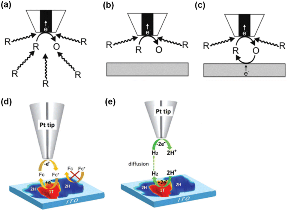 | ||
| Scheme 1 SECM operational modes. (a) Steady-state behavior in bulk solution. (b) Negative feedback mode over an inert substrate. (c) Positive feedback effect mode over a conducting substrate. (d and e) Schematic illustration of SECM imaging over MoS2 nanosheets by the oxidation/reduction of Fc in the feedback mode (d) and probing the HER at MoS2 in the SG/TC mode (e). (a–c) The schemes were reproduced and adapted with permission from Polcari et al.59 Copyright 2016, ACS. (d and e) The schemes were reproduced and adapted with permission from Sun et al.108 Copyright 2019, RSC. | ||
2.3 Introduction to SECCM mapping
SECCM is a scanning electrochemical technique using a fluidic nanopipette probe to carry out local electrochemistry at controlled sites of a substrate.25,68,69 A nanopipette probe filled with electrolyte solution is positioned near a substrate (usually exposed in the air). Upon contact, the meniscus of the solution inside the nanopipette formed a droplet cell on the substrate, and the electrochemical properties of the local site under the droplet can be studied by collecting a voltammogram on the probe. And by retracting the probe and approaching to the substrate at other locations, the electrochemical properties at various sites of the substrate can be visualized (Scheme 2a). After SECCM mapping over a substrate, residues of the dried electrolyte can be observed via SEM, as shown in Scheme 2b, which is helpful for identifying the exact locations studied on the substrate.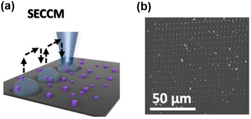 | ||
| Scheme 2 (a) Illustration of the SECCM imaging over the Co3O4 nanocubes. (b) SEM image of the substrate after SECCM mapping. The sites imaged by the probe can be visualized by the residues due to the dried electrolyte. Locations with interest, i.e. locations showing a higher current signal, can be further characterized by SEM. The schemes were reproduced and adapted with permission from Quast et al.85 Copyright 2021, Wiley. | ||
2.4 Challenges of nanoscale SECM and SECCM measurements
Several prerequisites about the UME and the substrate should be met to enable nanoscale SECM or SECCM measurements. A reliable nanoelectrode with controllable shape is required to achieve nanoscale resolution. Additionally, flat and homogenous substrates are often preferred, e.g., silicon wafer and HOPG, since good flatness of the substrate facilitates the positioning of an UME nearby. A rough surface hinders the approach curve in SECM experiments, and it is challenging to avoid crushing the UME into the substrate when conducting SECCM mapping over a rough surface. Moreover, surface features such as protrusion or recession on the substrate would lead to changes in the current signals, complicating the analysis of surface reactions. Due to these prerequisites, nanoscale SECM and SECCM measurements are challenging and a large portion of research is conducted on flat substrates such as Pt, HOPG, silicon wafer and glass plates.3. Study of HER and OER on 0D nanomaterials deposited on nanoelectrodes
3.1 HER on isolated Pt single atoms, small clusters and NPs
Pt is one of the most traditional and most widely used electrocatalytic materials for the HER. Using the nanoelectrodes as the substrate, the controlled electrodeposition of isolated single Pt atoms on the nanoelectrode followed by immediate electrochemical characterization on the deposit became feasible. Recently, the size and substrate effect on the HER have been studied on single isolated Pt atoms, atomic clusters and NPs.70 An atom-by-atom methodology was applied to electrodeposit an isolated single Pt atom,71,72 atomic cluster or NP on Bi and Pb UMEs with ∼120 nm radius. Pt atoms are deposited from H2PtCl6 solutions with fM level concentration with a deposition rate of about 10 s Pt per atom. Due to the ultra-small tip size and limited active sites on UMEs, the deposition and growth at more than one site are highly unlikely, allowing for a control over the number of atoms deposited and the size of the deposit.After electrodeposition, the UME was characterized by voltammetry to study the HER activity in a solution of 40 mM HClO4 and 0.2 M NaClO4, where the heterogeneous electron transfer (ET) kinetics of the HER was obtained. Typical HER voltammograms on a single isolated Pt atom supported on the Bi and Pb substrate are shown in Fig. 1a and b. The Bi and Pb UMEs were inert towards HER as shown in the background signal, and a diffusion-limited plateau was observed due to the HER on the Pt atom. The HER ET kinetics at a single atom or small clusters and NPs was analyzed by fitting the voltammogram using the Butler–Volmer equation. The HER at atoms, clusters, and NPs was assumed to follow the same general mechanism as the HER on bulk Pt, where a 1e Volmer step is considered to be the rate determining step. The authors hypothesized that the standard potential of the Volmer step, E° = 0 V vs. normal hydrogen potential (NHE) for Pt atoms, clusters and NPs for the Volmer step, and calculated standard electron transfer rate constant k0 and transfer coefficient α of the Volmer step, assuming a hemispherical geometry of the Pt atom, cluster or NP. The authors found that for a single Pt atom deposited on the Bi substrate, k0 = 1.06 × 10⁻³ cm s−1 and α = 0.49, while k0 = 4.36 × 10⁻⁶ cm s−1 and α = 0.52 for the case of the Pb substrate. Note that there is a large HER kinetics difference between the single Pt atoms on different substrates.
 | ||
| Fig. 1 (a, c and e) Forward scan voltammograms of the HER on a single Pt atom, a single Pt cluster and a single Pt NP with varying sizes deposited on the Bi UME. (b, d and f) Forward scan voltammograms of the HER on a single Pt atom, a single Pt cluster and a single Pt NP with varying sizes deposited on the Pb UME. For figures (a–f), the solution contained 40 mM HClO4 and 0.2 M NaClO4. The scan rates were 50 mV s−1. BG, EXP and SIM refer to the background, experiment and simulation curves, respectively. (g) Extracted k0 as a function of the radius of a single Pt deposit on Bi and Pb substrates. As a comparison, the HER kinetics on the Pb substrate is magnified by 200 times. (h) SEM image of a Pt NP deposited on a carbon UME using the same technique. (a–g) The figures were reproduced and adapted with permission from Zhou et al.70 Copyright 2019, ACS. (h) The figure was reproduced and adapted with permission from Ma et al.72 Copyright 2017, ACS. | ||
The typical HER voltammograms for Pt clusters and Pt NPs are shown in Fig. 1c to f. It was found that as the size of a single cluster or NP (rNP) increased, the half-wave potential (E1/2) of the voltammogram shifted positively, which was attributed to a change in the deposit size as well as a change in the kinetics.73 Curve fitting analysis was performed for voltammograms obtained on different sized Pt clusters and NPs, as shown in Fig. 1g, where an increase in HER activity was obtained as the size of the cluster or NP increased. A limiting plateau was reached as the NP size became about 4 nm, indicating a limiting k0. The limiting k0 for Pt NP on a Bi substrate was ∼0.1 cm s−1, close to that reported on bulk Pt (∼0.3 cm s−1), while the limiting k0 for Pt NP on a Pb substrate was ∼10−4 cm s−1. The difference in the HER kinetics on different substrates was attributed to different catalyst/support interactions between Pt and respective supporting substrates.
3.2 OER on cobalt-based molecules, clusters and NPs
Apart from noble metal based materials, tremendous amount of work has been devoted to the development of cost-efficient transition metal-based catalysts.74–77 Transition metal oxide catalysts for the OER have been frequently produced by electrodeposition,78–80 while using nanoelectrodes, the electrodeposition of a single cobalt oxide molecule became possible.81 Isolated cobalt oxide single molecules (Co1Ox) and clusters (ConOy) were electrodeposited on nanometer-size carbon fiber UMEs. The radius of the carbon fiber UME was 80 nm, which generally provides only a single site of nucleation during the electrodeposition reaction at ∼0.1 Hz deposition frequency, allowing for a controllable nucleation process. The OER was then carried out on the deposited nanoelectrode in 10 mM NaOH and 0.2 M NaClO4. The shape of the deposited molecule or cluster was assumed to be a hemisphere, and the equivalent radius rd was calculated from the limiting current of the voltammogram, where the smallest size obtained was 0.21 nm, close to the reported distance of Co–O in CoO6 octahedra (1.89 Å).82 This suggests the formation of a single cobalt oxide molecule (Co1Ox). Similarly, larger calculate rd values suggested other ConOy (n = 2, 3, 4) clusters. The size-dependent catalytic activity was studied by comparing Ek, the potential at a current density of 2.5 pA nm−2 in the voltammogram. Ek increased as rd increased, suggesting that the single cobalt oxide molecule has the lowest overpotential for the OER. This trend is likely due to the fact that in the deposited cobalt oxide structure, Co(IV) is probably the active site for catalyzing the OER, and the Co(IV) site per unit area decreases as the cluster size increases.Apart from the cobalt oxide molecule and clusters, progress has been made on the OER electrocatalysis on cobalt-based single NP with controlled shape prepared on nanoelectrodes.83–85 A single cobalt-based MOF nanocrystal was grown on a carbon nanoelectrode (CNE) surface with a radius of 300 nm, which was then pyrolyzed to generate a cobalt/nitrogen-doped carbon (CoN/C) NP.83 MOFs are formed by the coordination of the central metal and organic ligands,86 and due to their excellent properties, such as the crystalline structure, high surface area and rich active sites, MOFs have been applied in many fields.87–91 Using the MOF nanocrystal grown on the CNE as the template leads to CoN/C NPs with a designed shape.92 The synthesized CoN/C NPs showed high OER activity in 0.1 M KOH at 200 mV s−1 scan rate, with a current density of 230 mA cm−2 at 1.77 V vs. reversible hydrogen electrode (RHE). It is impossible to achieve this high current density under industrial conditions on macroelectrodes.
A physical “pick-and-drop” technique was developed to deposit Co3O4 NPs on the CNE surface.84 The CNE with a radius of 250–300 nm was prepared and trimmed by focus ion beam (FIB), and then the surface-modified with N-Boc-ethylenediamine to improve the chemical compatibility between the nanoparticles and the carbon surface. Hexagonal-shaped Co3O4 NPs of 180–300 nm were synthesized93 and drop-coated on a gold wafer under the inspection via SEM. A micromanipulator arm mounted in the SEM chamber was used to isolate the desired Co3O4 NP, followed by picking up the NP by contact using the slowly moving tip of the micromanipulator arm (<5 nm per increment). The NP was delivered to several mm above the CNE surface and carefully placed onto the CNE surface to create the Co3O4@CNE nanoassembly, which was further confirmed by SEM, TEM and energy dispersive spectroscopy (EDS) measurements. The OER activity of the Co3O4@CNE was characterized in 1 M KOH at a scan rate of 200 mV s−1, as shown in Fig. 2a–c, and a current density up to 11.5 A cm−2 at 1.92 V vs. RHE was observed.
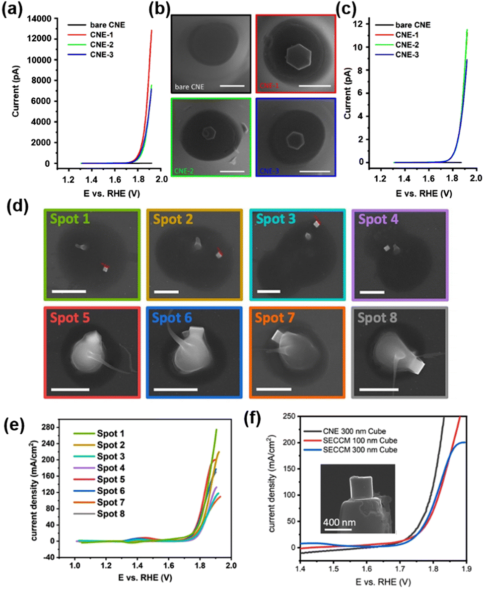 | ||
| Fig. 2 (a) Linear sweep voltammograms (LSV) of the three independent Co3O4@CNE nanoassemblies. The LSV was recorded in 1 M KOH with a scan rate of 200 mV s−1. (b) Corresponding SEM images of the Co3O4@CNE nanoassemblies. Scale bars: 400 nm. (c) LSV in (A) normalized by the electrochemical active surface area. (d) SEM images showing the selected droplet-landing spots from a SECCM scan with a single Co3O4 spinel nanocube located within the droplet. The residues are due to the dried KOH electrolyte. Scale bars: 1 μm. (e) LSV recorded from Co3O4 spinel nanocubes in 0.05 M KOH containing 0.1 mM Os-complex solution with a scan rate of 1 V s−1. The color code corresponds to that in (D). (f) LSV spectra recorded from the single Co3O4@CNE nanoassembly (black) and by means of SECCM (blue and red) in 0.05 M KOH containing 0.1 mM Os-complex solution with a scan rate of 1 V s−1. Inset: SEM image of a Co3O4 spinel nanocube on the CNE. (a–c) The figures were reproduced and adapted with permission from Quast et al.84 Copyright 2021, Wiley. (d–f) The figures were reproduced and adapted with permission from Quast et al.85 Copyright 2021, Wiley. | ||
Furthermore, the OER catalytic properties of Co3O4 nanocubes were studied by SECCM as well as by voltammograms on a Co3O4@CNE nanoassembly.85 Co3O4 nanocubes were synthesized and then dispersed in toluene and drop-coated onto a polished glassy carbon plate. Nanopipettes with radius between 200 and 250 nm were used as probes of SECCM, and a hopping-mode SECCM scan over the glassy carbon plate was performed over an area of 100 × 100 μm2 with a hopping distance of 7 to 10 μm, creating 2300 landing sites in total. At each landing site, a linear sweep voltammogram (LSV) was performed to determine the OER activity of the site wetted by the meniscus of the nanopipette. Spots with higher current responses were analyzed via SEM to visualize the presence of Co3O4 nanocubes. As shown in Fig. 2d and e, although nanocubes with varying sizes were present, a similar activity of the OER was observed after normalization to the geometric surface area. The highest current density at 1.9 V vs. RHE is 275 mA cm−2. Co3O4 nanocubes were also “pick-and-dropped” onto the CNE to verify the OER activity studied by SECCM. The comparison between the OER activity from Co3O4@CNE and that from SECCM is shown in Fig. 2f. At lower current densities, the signal obtained by Co3O4@CNE (123 mA cm−2 at 1.8 V vs. RHE) was similar to that obtained by SECCM (81 mA cm−2 at 1.8 V vs. RHE). However, with increasing overpotential, the difference in the current signal of the two techniques became large, which is due to the restricted electrolyte volume and diffusional constraints in the SECCM configuration.
The authors further studied the effect of the shape of NP on the OER activity. LSV on Co3O4@CNE in 1 M KOH was performed at a scan rate of 200 mV s−1, and a current density of 5.5 A cm−2 at 1.92 V vs. RHE was obtained. This was about half of that observed on hexagonal Co3O4@CNE under the same condition (11.5 A cm−2),84 which is likely due to the comparatively low number of Co atoms on the (100) plane.
4. Nanoelectrode-based study of the HER and OER on 2D nanomaterials
4.1 Nanostructured MoS2 for HER study
Molybdenum disulfide (MoS2) has attracted a lot of attention as an abundant and low-cost alternative catalyst for the HER. Following the early study on bulk crystals of MoS2,94 the general consensus about the HER activity on MoS2 is that the edges of the 2H phase are catalytically active, while the basal plane is inert for the HER.95–99 However, the direct comparison of HER activity at the basal plane and at the edges has been challenging due to the ultrasmall size of the edge plane. An electrochemical technique with nanoscale spatial resolution is required for the distinguishment of the HER at edges from that of the basal plane. Using nanoelectrodes as the probe, the HER activity on natural crystals of MoS2 at the basal plane and edge plane has been studied by SECCM.100MoS2 crystals were prepared by mechanical exfoliation, and dual-barrel nanopipettes were used as the probe of SECCM. The orifice of the nanopipette has an elliptical shape, with the major and minor radii of ∼250 nm and ∼130 nm, respectively. The authors applied SECCM mapping of HER activity on MoS2 at both low proton concentration (5 mM) and high concentration (100 mM), where the nanopipette was approached to the substrate at a series of locations with 1 μm spacing and recording the LSV at each location wetted by the meniscus of the probe. An imaging over the MoS2 is shown in Fig. 3a and b, where regions with higher current signals were observed. The higher current was attributed to the increased HER activity at the regions due to the presence of surface defects, as confirmed by LSV, SEM and AFM measurements (Fig. 3c–e). AFM line profile scanning over the defects revealed a step edge structure, likely composed of several to tens of MoS2 layers. The HER LSV at the basal plane and the defects were collected, area normalized and analyzed through the Tafel plot as shown in Fig. 3c and f and g, where the Tafel slopes and exchange current J0 were extracted. The authors reported J0 to be 2.5 × 10⁻⁶ A cm−2 on the basal plane, comparable to that reported in the literature,101 and about 3 orders of magnitudes lower than that of polycrystalline Pt (∼2.5 × 10⁻³ A cm−2). On the other hand, J0 on the edge plane was estimated to be ∼1 × 10⁻⁴ A cm−2, indicating a significantly higher HER activity than that on the basal plane.
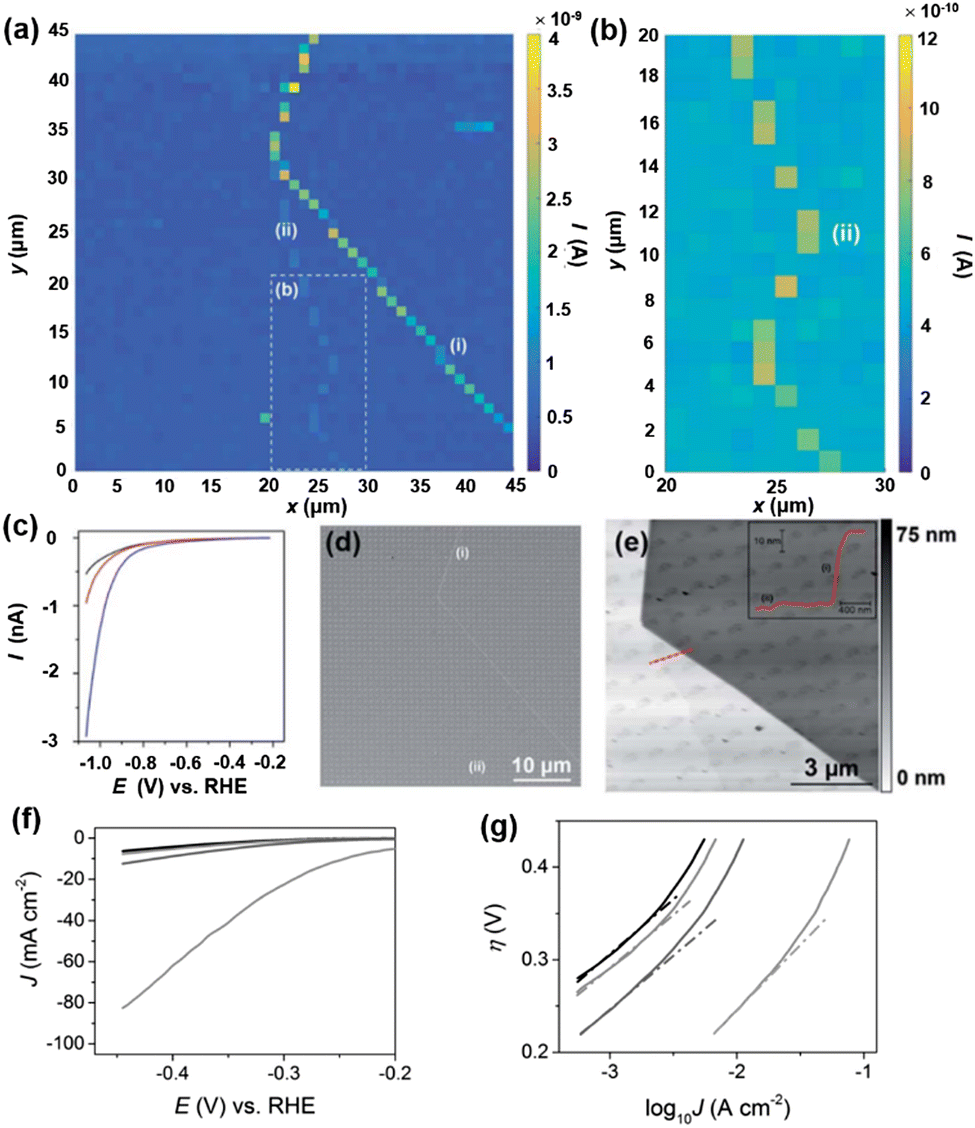 | ||
| Fig. 3 (a) 45 × 45 μm and (b) 10 × 20 μm (area indicated by the dashed white box in (a) spatially resolved current map over MoS2 obtained at −1.05 V vs. RHE in 100 mM HClO4. Major and minor surface defects are labelled as (i) and (ii), respectively. (c) Representative LSVs from areas containing only basal plane (black trace), basal plane plus defect (i) (blue trace) and basal plane plus defect (ii) (red trace). (d) SEM and (e) AFM topographical images of the scan area. The inset in (e) is an AFM line scan profile of the area indicated by the red line. (f) LSVs (area normalized) and (g) Tafel plots obtained from the MoS2 basal plane (black trace), MoS2 basal plane plus defect (i) (blue trace), MoS2 basal plane plus defect (ii) (red trace) and MoS2 edge plane (pink trace). The solution contained 100 mM HClO4. Scan rate: 0.25 V s−1. The figures were reproduced and adapted with permission from Bentley et al.100 Copyright 2017, RSC. | ||
Moreover, it has been recently found that nanostructured MoS2 is a promising catalyst for the HER,102–105 and the metallic 1T phase MoS2 outperformed the thermodynamically stable semiconducting 2H phase.95,106,107 Recently, the HER on metallic and semiconducting MoS2 nanosheets was studied by SECM using Pt nanoelectrodes, where SECM imaging over the MoS2 nanosheet revealed the presence of 1T phase, 2H phase and the 1T/2H boundary on the same nanosheet.108 Mixed-phase MoS2 nanosheets were prepared on indium tin oxide (ITO) coated glass, and SECM imaging over the mixed-phase MoS2 nanoflakes was carried out using Pt nanoelectrodes with the radius of 18 to 60 nm. SECM imaging revealed the presence of the 1T and 2H phases, based on different activities towards Fc oxidation and HER of the two phases. The presence of different phases on the nanosheets have also been confirmed by scanning transmission electron microscopy (STEM) and electron energy loss spectroscopy (EELS) measurements, which revealed the spatial variation in the atomic bonding environment. Furthermore, the authors characterized the local surface potentials over the nanosheets via scanning Kelvin probe microscopy (SKPM) and observed ∼250 mV surface potential difference between the probe tip and the mixed-phase MoS2 nanoflake, while only a ∼50 mV surface potential difference was observed on a pure 2H MoS2 nanoflake. The authors suggested this change in surface potential difference to be a result of the shallower work function of the mixed-phase MoS2 compared with 2H MoS2, which was consistent with the higher HER activity observed for the mixed-phase MoS2.
4.2 OER on nanoscale facets at the edge of NiO nanosheets
Nickel oxide (NiO) is an efficient catalyst for the OER.109,110 NiO with nanostructures showed improved OER activity, suggesting that the exposure of nanoscale facets/corners and edges could play an important role in the improved activity.111–113 However, it has been difficult to characterize the electrocatalytic properties of edges when their size is on the atomic scale.114,115 To overcome this difficulty, Pt nanoelectrodes were used as the probe of SECM to provide a sub-20 nm lateral resolution for the study of OER activity on a semi-2D nickel oxide nanosheet, and the OER catalytic properties at the edge of the nanosheet were found to be ∼200 times higher than that on the basal plane.116Semi-2D NiO nanosheets were prepared over a HOPG substrate using the hydrothermal method, which resulted in 10–20 nm thick, flat and single-crystalline slabs containing hexagonal defect holes with well-defined edges. The size of the defect holes ranged from tens to hundreds of nanometers. Pt nanoelectrodes were positioned near the HOPG substrate covered NiO nanosheets, and SECM imaging was carried out in both feedback mode and SG/TC mode, in a solution of 1 mM KOH, 1 mM Fc and 0.1 M KCl. As shown in Fig. 4a, when the Pt nanoelectrode scanned over the substrate in the feedback mode detecting Fc, the tip current was stable in the initial region, which then continuously decreased over ∼50–70 nm tip displacement along the x-axis, followed by another region with stable but lower current. The authors attributed this behavior to the different activity of the substrate, i.e., the tip was over the HOPG region initially, which then moved over to a nearby NiO nanosheet. Fc regeneration was fast over HOPG, which resulted in a positive feedback effect and a higher tip current. In contrast, NiO showed slow activity towards Fc regeneration, so that a negative feedback effect, i.e., a lower current, was observed. However, when the SECM imaging was carried out in the SG/TC mode to detect the product of the OER occurring on the NiO nanosheet, the current over the NiO region became higher than that over the HOPG region due to the OER activity of the NiO nanosheet, as shown in Fig. 4b. More importantly, a peak behavior was observed between the NiO region and HOPG region, indicating an even higher OER activity at the edge of NiO as shown in Fig. 4c.
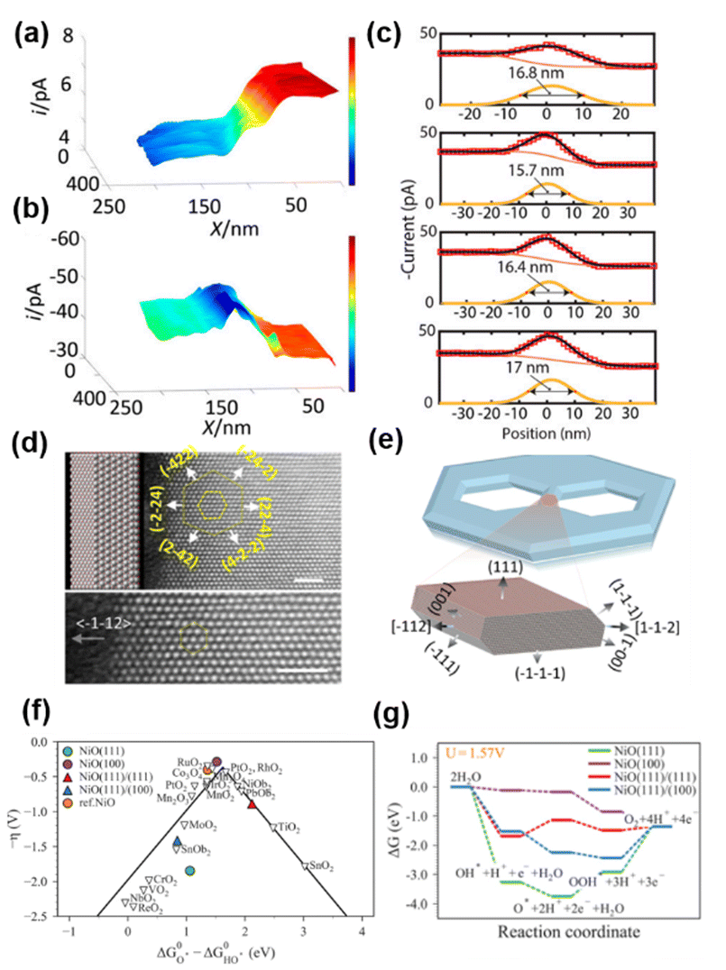 | ||
| Fig. 4 (a) Feedback mode and (b) SG/TC SECM images of the NiO edge. Pixel density 330/μm (x axis) and 100/μm (y axis). (c) Four experimental line scans across the NiO nanosheet edge recorded in the SG/TC mode. A tip radius of ∼20 nm. Solution contained 0.001 M KOH, 0.001 M Fc, and 0.1 M KCl. The tip was biased at 0.5 V vs. Ag/AgCl in (A), and −0.6 V in (b and c). The substrate was biased at the open circuit potential in (A) and biased at 0.9 V in (b and c). (d) Atomic-resolution Z-contrast STEM imaging of the nanosheet when it is laid down flat. (e) A computer-generated model of the nanosheet and the 3D atomistic model of the edges. (f) Standard free-energy diagram for the OER at the experimentally applied potential (U = 1.57 V). (g) The activity volcano plot of the OER. The figures were reproduced and adapted with permission from Sun et al.116 Copyright 2019, PNAS. | ||
The authors then reconstructed the 3D structures at the edges by collecting TEM images of the NiO nanosheets with −70° to 70° tilt and reconstructing the tomograms using a multiplicative simultaneous iterative reconstruction technique (Fig. 4d and e).117 It was found that compared with the basal plane, the edges were terminated with three additional coordination: the {100} facet, the edge between the {111} basal plane and the {111} nanofacets, and the edge between the {100} and {111} nanofacets. Furthermore, a free energy diagram was obtained for each step during the OER using density functional theory with the generalized gradient approximation at the Perdew–Burke–Ernzerhof level with spin-orbital approximation as shown in Fig. 5f and g. The (100) surface was found to have the lowest overpotential, followed by the (111)/(111) edge and (111)/(100) edge, and the (111) surface has the highest overpotential. Additionally, at the potential applied in SECM imaging, only on the (100) surface, the reaction free energy continues with the downward direction, facilitating the OER. The above results indicated that the (100) nanofacet at the edge is responsible for the catalytic enhancement. The authors then simulated the line scans over the NiO edge with different ratios of the OER current densities at the edge and at the edge. The current density at the edge must be ∼200 times higher than that at the basal plane to create a current change similar to that observed in the SECM experiment.
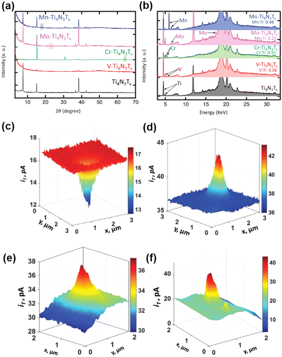 | ||
| Fig. 5 (a) XRD patterns for the exfoliated Ti4N3Tx MXene (black), V-Ti4N3Tx (red), Cr-Ti4N3Tx (green), Mo-Ti4N3Tx (pink) and Mn-Ti4N3Tx (blue). The boxes represent crystalline Cr, Mo, and Mn, respectively. (b) XRF spectra for X-ray diffraction patterns for the exfoliated Ti4N3Tx MXene, V-Ti4N3Tx, Cr-Ti4N3Tx, Mo-Ti4N3Tx and Mn-Ti4N3Tx. The color code is the same as in (a). (c and e) SECM feedback mode and (d and f) corresponding SG/TC mode SECM images of V-Ti4N3Tx. The solution contains 1 mM Fc and 0.1 M KCl (c and e), 0.5 mM Fc, 0.1 M KCl and 10 mM HClO4 (d), 0.5 mM Fc, 0.1 M KCl and 5 mM HClO4 (f). The tip is biased at 0.4 V vs. Ag/AgCl in (c and e) and biased at 0.5 V vs. Ag/AgCl in (d and f). The substrate was unbiased in (c and e) and biased at −0.6 V vs. Ag/AgCl in (d and f). The figures were reproduced and adapted with permission from Djire et al.121 Copyright 2020, Wiley. | ||
4.3 HER on mixed metal nitride MXenes
MXenes stands for a family of 2D transition metal carbides and nitrides, where promising electrochemical properties including good HER activities have been obtained.118–120 In a recent progress, Ti4N3Tx (Tx = O and/or OH) MXenes have been manipulated with transition metals alloyed into the basal plane, and the HER on these mixed metal MXenes was studied by SECM using Pt nanoelectrodes.121 The authors demonstrated that by manipulating the basal plane of mixed transition metal nitride MXenes M-Ti4N3Tx (M = V, Cr, Mo, or Mn), the HER activity can be tuned and the character of M-Ti4N3Tx can be adjusted from semiconducting to more metallic.First, the Ti4N3Tx MXenes were synthesized from Ti4N3Tx MAX phase through the oxygen-assisted etching process and exfoliation. Ti4N3Tx MXenes were then alloyed with transition metals using the corresponding salts to create M-Ti4N3Tx; for example, VOSO4·xH2O was used for the alloying of V-Ti4N3Tx. The mixed metal MXenes were characterized by X-ray diffraction (XRD) and X-ray fluorescence (XRF) to confirm the composition (Fig. 5a and b). The HER activity of the mixed transition metal MXenes was characterized by cyclic voltammetry and LSV in 0.5 M H2SO4, and different HER activities were observed for different transition metals incorporated in M-Ti4N3Tx, in the order of V-Ti4N3Tx > Cr-Ti4N3Tx > Mo-Ti4N3Tx > Mn-Ti4N3Tx, by comparing the overpotential at −10 mA cm−2 in the LSV. The trend is also consistent with the Tafel plot and the charge transfer resistance in electrochemical impedance spectra.
The authors further characterized the electrochemical activities of the nanoflakes of the above MXenes using SECM, with Fc as the mediator. The nanoflakes were positioned on ITO glass substrates. The ITO substrate has a reasonable activity for the reduction of Fc+ but is inert towards the HER. A nanoelectrode with the radius ranging from 40 to 280 nm was positioned close to the nanoflake (∼50 nm distance), and constant height imaging over the nanoflakes and the underlying ITO substrate was conducted both in the feedback mode (in 1 mM Fc, 0.1 M KCl solution) and in the SG/TC mode (in 0.5 mM Fc, 10 mM HClO4, 0.1 M KCl solution). As shown in Fig. 5c, in the feedback mode for the detection of Fc, the current over the nanoflakes was lower than that over ITO. This behavior was observed for all the MXene nanoflakes, which indicated that the reduction of Fc+ to Fc on the nanoflakes was very slow. However, when operated in the SG/TC mode to detect hydrogen generated by the HER on MXene, the current over the V-Ti4N3Tx nanoflakes (Fig. 5d) and Cr-Ti4N3Tx nanoflakes was higher than that over ITO, which meant that these nanoflakes showed some activity toward the HER, suggesting that V-Ti4N3Tx and Cr-Ti4N3Tx behaved like semi-conductors. According to the SECM imaging results, V-Ti4N3Tx nanoflakes showed higher HER activity than Cr-Ti4N3Tx. On the other hand, Mo-Ti4N3Tx and Mn-Ti4N3Tx showed low electrical conductivity and HER activity, exhibiting a negative feedback effect in both feedback mode and SG/TC mode of SECM imaging. The above SECM imaging study revealed the same trend of HER activity as the LSV results.
Furthermore, the authors were able to increase the V loading inside the nanoflakes by augmenting the concentration of the precursor solution of VOSO4·xH2O during synthesis. Fig. 5e shows the SECM imaging of the V-Ti4N3Tx nanoflake in the feedback mode, where a positive feedback effect was observed when the sample was unbiased, indicating a fast generation of Fc on the nanoflake with metallic character. Due to the more metallic character, HER activity of the V-Ti4N3Tx sample was also enhanced as shown in Fig. 5f.
5. Summary and outlook
In this review, we summarized the recent progress in the nanoelectrode-based studies on the HER and OER of catalytic materials with nanostructures, including the in situ electrochemical characterization of 0D single entities grown on the nanoelectrodes, and the study of surface features, i.e., defects and edge plane, different phases and nanofacets, on 2D nanomaterials.More fundamentally, the current signals from these materials were analyzed for the extraction of kinetic information and the quantitative comparison of the material activities, as summarized in Table 1. For the HER activity, due to the simpler mechanism, researchers were able to extract the intrinsic kinetic parameters such as k0 and J0 on various materials, which can be directly used for the comparison of HER activities. On the other hand, in the study of OER activity, due to the complicated mechanism, the intrinsic kinetic parameters have not been analyzed, and current densities at given potentials were used as the quantitative criteria when comparing OER activities. On top of the fact that several potentials have been chosen, we should bear in mind that current densities collected from voltammograms are also affected by the experimental conditions such as OH− concentration and scan rates. This suggests that extra caution should be taken when comparing OER activities across different materials.
| Materials | Water catalysis reaction | Technique | Kinetic information | Current density at a certain potential | Ref. |
|---|---|---|---|---|---|
| a The kinetic information of AuNPs is listed here for reference. b Solution contained 0.5 M H2SO4, scan rate: 5 mV s−1. c Solution contained 10 mM NaOH and 0.2 M NaClO4, scan rate: 10 mV s−1. d Solution contained 0.1 M KOH, scan rate: 200 mV s−1. e Solution contained 1 M KOH, scan rate: 200 mV s−1. | |||||
| Pt single atom, clusters and NPs | HER | Nanoelectrode-based CV | Limiting k0 ∼ 0.1 cm s−1 on Bi substrate), limiting k0 ∼ 10−4 cm s−1 (on Pb substrate) | — | 70 |
| AuNPa | HER | SECM approach curve | k 0 = 3.4 cm s−1 | — | 52 |
| MoS2 basal plane and step edges | HER | SECCM mapping | J 0 ∼ 2.5 × 10⁻⁶ A cm−2 (basal plane), J0 ∼ 1.0 × 10⁻⁴ A cm−2 (edge plane) | — | 100 |
| MoS2 nanosheets | HER | SECM imaging | 1T phase has much higher HER activity than 2H phase | — | 108 |
| Mixed transition metal Ti4N3Tx MXenes nanoflakes | HER | SECM imaging | The order of HER activity: V-Ti4N3Tx> Cr-Ti4N3Tx > Mo-Ti4N3Tx > Mn-Ti4N3Tx | 10 mA cm−2 at 0.33–0.61 V vs. RHE (material dependent)b | 121 |
| Co1Ox and ConOy NPs | OER | Nanoelectrode-based CV | — | 2.5 pA cm−2 at 1.75–1.88 V vs. RHE (size dependent)c | 81 |
| CoN/C NPs | OER | Nanoelectrode-based CV | — | 230 mA cm−2 at 1.77 V vs. RHEd | 83 |
| Hexagonal Co3O4 NPs | OER | Nanoelectrode-based LSV | — | 11.5 A cm−2 at 1.92 V vs. RHEe | 84 |
| Co3O4 nanocubes | OER | Nanoelectrode-based LSV, SECCM mapping | — | 5.5 A cm−2 at 1.92 V vs. RHEe | 85 |
| NiO nanosheets | OER | SECM imaging | OER activity at the (100) nanofacet at the edge is ∼200 times higher than that on the basal plane | — | 116 |
A deeper understanding of the reaction mechanisms of the HER and OER will greatly facilitate the development of renewable and sustainable energy generation based on water electrocatalysis. Promising advances have been made to unveil complicated reaction mechanisms with sub-micrometer UME-based SECM,122,123 and we believe that continuous efforts with nanoelectrodes can contribute greatly to the understanding of the HER and OER mechanisms as well as the development of catalysts for water electrocatalysis. Additionally, the development of new electrochemical techniques brings more tools for nanoscale electrochemical characterization. For example, a novel imaging technique based on the SECM approach curve has been recently developed that can analyze the surface electroactivity on nonflat substrates.124 This opens up opportunities for the nanoscale electrochemical study of catalysts with more surface roughness. On the other hand, apart from the HER and OER, there is a huge amount of work on the development of innovative catalytic materials for different intriguing reactions, such as the oxygen reduction reaction (ORR), CO2 reduction and N2 reduction, and the application of nanoelectrodes has led to pioneering work in understanding the mechanism of the ORR and CO2 reduction.29,125 We envision that the application of nanoelectrodes in the research of these catalysts can lead to promising advances in the development of sustainable energy and help solve CO2 release issues.
Author contributions
Writing-original draft, R. C.; writing-review & editing, Y. Z. and S. L.; funding acquisition, R. C and Y. Z.; supervision, Y. Z.Conflicts of interest
There are no conflicts to declare.Acknowledgements
This research was funded by the National Natural Science Foundation of China (22102025 and 22174014), the 2021 Shuangchuang (Mass Innovation and Entrepreneurship) Talent Program of Jiangsu Province (JSSCBS20210063), and the Zhishan Young Scholar Program of Southeast University.Notes and references
- J. A. Turner, Science, 2004, 305, 972–974 CrossRef CAS PubMed.
- S. Chu and A. Majumdar, Nature, 2012, 488, 294–303 CrossRef CAS PubMed.
- K. J. Lee, N. Elgrishi, B. Kandemir and J. L. Dempsey, Nat. Rev. Chem., 2017, 1, 0039 CrossRef CAS.
- E. S. Rountree, B. D. McCarthy, T. T. Eisenhart and J. L. Dempsey, Inorg. Chem., 2014, 53, 9983–10002 CrossRef CAS PubMed.
- C. Costentin and J.-M. Savéant, ChemElectroChem, 2015, 2, 1774–1784 CrossRef CAS.
- B. D. McCarthy, A. M. Beiler, B. A. Johnson, T. Liseev, A. T. Castner and S. Ott, Coord. Chem. Rev., 2020, 406, 213137 CrossRef CAS PubMed.
- J. M. Jaksic, F. Nan, G. D. Papakonstantinou, G. A. Botton and M. M. Jaksic, J. Phys. Chem. C, 2015, 119, 11267–11285 CrossRef CAS.
- R. M. Wightman and D. O. Wipf, in Electroanalytical Chemistry, ed. A. J. Bard, Marcel Decker, New York, 1989, vol. 15, ch. 267 Search PubMed.
- J. Heinze, Angew. Chem., Int. Ed. Engl., 1993, 32, 1268–1288 CrossRef.
- D. W. M. Arrigan, The Analyst, 2004, 129, 1157 RSC.
- R. W. Murray, Chem. Rev., 2008, 108, 2688–2720 CrossRef CAS PubMed.
- Y. Fan, C. Han and B. Zhang, The Analyst, 2016, 141, 5474–5487 RSC.
- R. Chen, K. Alanis, T. M. Welle and M. Shen, Anal. Bioanal. Chem., 2020, 412, 6121–6132 CrossRef CAS PubMed.
- J. Clausmeyer and W. Schuhmann, TrAC, Trends Anal. Chem., 2016, 79, 46–59 CrossRef CAS.
- L. Luo and H. S. White, Langmuir, 2013, 29, 11169–11175 CrossRef CAS PubMed.
- Q. Chen, L. Luo, H. Faraji, S. W. Feldberg and H. S. White, J. Phys. Chem. Lett., 2014, 5, 3539–3544 CrossRef CAS PubMed.
- J. Kim, B.-K. Kim, S. K. Cho and A. J. Bard, J. Am. Chem. Soc., 2014, 136, 8173–8176 CrossRef CAS PubMed.
- X. Li, S. Majdi, J. Dunevall, H. Fathali and A. G. Ewing, Angew. Chem., Int. Ed., 2015, 54, 11978–11982 CrossRef CAS PubMed.
- X.-W. Zhang, Q.-F. Qiu, H. Jiang, F.-L. Zhang, Y.-L. Liu, C. Amatore and W.-H. Huang, Angew. Chem., Int. Ed., 2017, 56, 12997–13000 CrossRef CAS PubMed.
- K. Hu, E. Relton, N. Locker, N. T. N. Phan and A. G. Ewing, Angew. Chem. Int. Ed., 2021, 60, 15302–15306 CrossRef CAS PubMed.
- J. Kim and A. J. Bard, J. Am. Chem. Soc., 2016, 138, 975–979 CrossRef CAS PubMed.
- R. Chen, K. Hu, Y. Yu, M. V. Mirkin and S. Amemiya, J. Electrochem. Soc., 2015, 163, H3032–H3037 CrossRef PubMed.
- M. Shen, R. Ishimatsu, J. Kim and S. Amemiya, J. Am. Chem. Soc., 2012, 134, 9856–9859 CrossRef CAS PubMed.
- R. Chen, R. J. Balla, A. Lima and S. Amemiya, Anal. Chem., 2017, 89, 9946–9952 CrossRef CAS PubMed.
- O. J. Wahab, M. Kang and P. R. Unwin, Curr. Opin. Electrochem., 2020, 22, 120–128 CrossRef CAS.
- Y. Wang, E. Gordon and H. Ren, Anal. Chem., 2020, 92, 2859–2865 CrossRef CAS PubMed.
- N. P. Siepser, M.-H. Choi, S. E. Alden and L. A. Baker, J. Electrochem. Soc., 2021, 168, 126526 CrossRef.
- Y. Shan, X. Deng, X. Lu, C. Gao, Y. Li and Q. Chen, Chin. Chem. Lett., 2022, 33, 5158–5161 CrossRef CAS.
- R. G. Mariano, K. McKelvey, H. S. White and M. W. Kanan, Science, 2017, 358, 1187–1192 CrossRef CAS PubMed.
- Y. Takahashi, Y. Kobayashi, Z. Wang, Y. Ito, M. Ota, H. Ida, A. Kumatani, K. Miyazawa, T. Fujita, H. Shiku, Y. E. Korchev, Y. Miyata, T. Fukuma, M. Chen and T. Matsue, Angew. Chem., Int. Ed., 2020, 59, 3601–3608 CrossRef CAS PubMed.
- Y. Yan, B. Y. Xia, B. Zhao and X. Wang, J. Mater. Chem. A, 2016, 4, 17587–17603 RSC.
- Z. Y. Yu, Y. Duan, X. Y. Feng, X. Yu, M. R. Gao and S. H. Yu, Adv. Mater., 2021, 33, 2007100 CrossRef CAS PubMed.
- L. Li, P. Wang, Q. Shao and X. Huang, Chem. Soc. Rev., 2020, 49, 3072–3106 RSC.
- C. Hu and L. Dai, Angew. Chem., Int. Ed., 2016, 55, 11736–11758 CrossRef CAS PubMed.
- H. Shi, Y. Shen, F. He, Y. Li, A. Liu, S. Liu and Y. Zhang, J. Mater. Chem. A, 2014, 2, 15704–15716 RSC.
- J. Wang, H. Kong, J. Zhang, Y. Hao, Z. Shao and F. Ciucci, Prog. Mater. Sci., 2021, 116, 100717 CrossRef CAS.
- A. Bavykina, N. Kolobov, I. S. Khan, J. A. Bau, A. Ramirez and J. Gascon, Chem. Rev., 2020, 120, 8468–8535 CrossRef CAS PubMed.
- H.-F. Wang, L. Chen, H. Pang, S. Kaskel and Q. Xu, Chem. Soc. Rev., 2020, 49, 1414–1448 RSC.
- D. Zhu, M. Qiao, J. Liu, T. Tao and C. Guo, J. Mater. Chem. A, 2020, 8, 8143–8170 RSC.
- Y. Fang, Y. Hou, X. Fu and X. Wang, Chem. Rev., 2022, 122, 4204–4256 CrossRef CAS PubMed.
- Y. Wang, H. Su, Y. He, L. Li, S. Zhu, H. Shen, P. Xie, X. Fu, G. Zhou, C. Feng, D. Zhao, F. Xiao, X. Zhu, Y. Zeng, M. Shao, S. Chen, G. Wu, J. Zeng and C. Wang, Chem. Rev., 2020, 120, 12217–12314 CrossRef CAS PubMed.
- Q. Zhang and J. Guan, Adv. Funct. Mater., 2020, 30, 2000768 CrossRef CAS.
- S. Sultan, J. N. Tiwari, A. N. Singh, S. Zhumagali, M. Ha, C. W. Myung, P. Thangavel and K. S. Kim, Adv. Energy Mater., 2019, 9, 1900624 CrossRef.
- B. Konkena, J. Masa, A. J. R. Botz, I. Sinev, W. Xia, J. Koßmann, R. Drautz, M. Muhler and W. Schuhmann, ACS Catal., 2016, 7, 229–237 CrossRef.
- M. Steimecke, G. Seiffarth and M. Bron, Anal. Chem., 2017, 89, 10679–10686 CrossRef CAS PubMed.
- S. Chakrabarty, A. Mukherjee, W.-N. Su and S. Basu, Int. J. Hydrogen Energy, 2019, 44, 1565–1578 CrossRef CAS.
- M. Tavakkoli, E. Flahaut, P. Peljo, J. Sainio, F. Davodi, E. V. Lobiak, K. Mustonen and E. I. Kauppinen, ACS Catal., 2020, 10, 4647–4658 CrossRef CAS.
- D. Jasion, J. M. Barforoush, Q. Qiao, Y. Zhu, S. Ren and K. C. Leonard, ACS Catal., 2015, 5, 6653–6657 CrossRef CAS.
- H. Li, M. Du, M. J. Mleczko, A. L. Koh, Y. Nishi, E. Pop, A. J. Bard and X. Zheng, J. Am. Chem. Soc., 2016, 138, 5123–5129 CrossRef CAS PubMed.
- J. Kim, C. Renault, N. Nioradze, N. Arroyo-Currás, K. C. Leonard and A. J. Bard, J. Am. Chem. Soc., 2016, 138, 8560–8568 CrossRef CAS PubMed.
- T. Sun, Y. Yu, B. J. Zacher and M. V. Mirkin, Angew. Chem., Int. Ed., 2014, 53, 14120–14123 CrossRef CAS PubMed.
- T. Sun, D. Wang and M. V. Mirkin, Angew. Chem., Int. Ed., 2018, 57, 7463–7467 CrossRef CAS PubMed.
- M. Choi, N. P. Siepser, S. Jeong, Y. Wang, G. Jagdale, X. Ye and L. A. Baker, Nano Lett., 2020, 20, 1233–1239 CrossRef CAS PubMed.
- J. L. Fernández and C. G. Zoski, J. Phys. Chem. C, 2018, 122, 71–82 CrossRef.
- Y. Zheng, Y. Jiao, M. Jaroniec and S. Z. Qiao, Angew. Chem., Int. Ed., 2014, 54, 52–65 CrossRef PubMed.
- Z. W. Seh, J. Kibsgaard, C. F. Dickens, I. Chorkendorff, J. K. Nørskov and T. F. Jaramillo, Science, 2017, 355, eaad4998 CrossRef PubMed.
- X. Xie, L. Du, L. Yan, S. Park, Y. Qiu, J. Sokolowski, W. Wang and Y. Shao, Adv. Funct. Mater., 2022, 32, 2110036 CrossRef CAS.
- T. Naito, T. Shinagawa, T. Nishimoto and K. Takanabe, Inorg. Chem. Front., 2021, 8, 2900–2917 RSC.
- D. Polcari, P. Dauphin-Ducharme and J. Mauzeroll, Chem. Rev., 2016, 116, 13234–13278 CrossRef CAS PubMed.
- Y. Li, X. Ning, Q. Ma, D. Qin and X. Lu, TrAC, Trends Anal. Chem., 2016, 80, 242–254 CrossRef CAS.
- L. Yao, F. P. Filice, Q. Yang, Z. Ding and B. Su, Anal. Chem., 2018, 91, 1548–1556 CrossRef PubMed.
- L. Yao, K. Chen and B. Su, Anal. Chem., 2019, 91, 15436–15443 CrossRef CAS PubMed.
- Y. Shao and M. V. Mirkin, J. Electroanal. Chem., 1997, 439, 137–143 CrossRef CAS.
- P. Sun, Z. Zhang, Z. Gao and Y. Shao, Angew. Chem., Int. Ed., 2002, 41, 3445–3448 CrossRef CAS PubMed.
- H. Xia, Z. Zhang, J. Liu, X. Ning, S. Zhang and X. Lu, Appl. Catal., B, 2019, 250, 189–199 CrossRef CAS.
- R. Chen, N. Nioradze, P. Santhosh, Z. Li, S. P. Surwade, G. J. Shenoy, D. G. Parobek, M. A. Kim, H. Liu and S. Amemiya, Angew. Chem., Int. Ed., 2015, 54, 15134–15137 CrossRef CAS PubMed.
- S. Kuermanbayi, Y. Yang, Y. Zhao, Y. Li, L. Wang, J. Yang, Y. Zhou, F. Xu and F. Li, Chem. Sci., 2022, 13, 10349–10360 RSC.
- C. L. Bentley, M. Kang and P. R. Unwin, Curr. Opin. Electrochem., 2017, 6, 23–30 CrossRef CAS.
- E. Daviddi, L. F. Gaudin and C. L. Bentley, Curr. Opin. Electrochem., 2022, 34, 101006 CrossRef CAS.
- M. Zhou, S. Bao and A. J. Bard, J. Am. Chem. Soc., 2019, 141, 7327–7332 CrossRef CAS PubMed.
- M. Zhou, J. E. Dick and A. J. Bard, J. Am. Chem. Soc., 2017, 139, 17677–17682 CrossRef CAS PubMed.
- W. Ma, K. Hu, Q. Chen, M. Zhou, M. V. Mirkin and A. J. Bard, Nano Lett., 2017, 17, 4354–4358 CrossRef CAS PubMed.
- K. B. Oldham and C. G. Zoski, J. Electroanal. Chem. Interfacial Electrochem., 1988, 256, 11–19 CrossRef CAS.
- J. Wang, W. Cui, Q. Liu, Z. Xing, A. M. Asiri and X. Sun, Adv. Mater., 2016, 28, 215–230 CrossRef CAS PubMed.
- M. Gong, D.-Y. Wang, C.-C. Chen, B.-J. Hwang and H. Dai, Nano Res., 2015, 9, 28–46 CrossRef.
- Y. Qin, Y. Sun, Y. Li, C. Li, L. Wang and S. Guo, Chin. Chem. Lett., 2020, 31, 774–778 CrossRef CAS.
- Q. Fu, J. Han, X. Wang, P. Xu, T. Yao, J. Zhong, W. Zhong, S. Liu, T. Gao, Z. Zhang, L. Xu and B. Song, Adv. Mater., 2020, 33, 1907818 CrossRef PubMed.
- M. W. Kanan and D. G. Nocera, Science, 2008, 321, 1072–1075 CrossRef CAS PubMed.
- Y. Surendranath, M. Dincǎ and D. G. Nocera, J. Am. Chem. Soc., 2009, 131, 2615–2620 CrossRef CAS PubMed.
- J. B. Gerken, J. G. McAlpin, J. Y. C. Chen, M. L. Rigsby, W. H. Casey, R. D. Britt and S. S. Stahl, J. Am. Chem. Soc., 2011, 133, 14431–14442 CrossRef CAS PubMed.
- Z. Jin and A. J. Bard, Proc. Natl. Acad. Sci. U. S. A., 2020, 117, 12651–12656 CrossRef CAS PubMed.
- M. W. Kanan, J. Yano, Y. Surendranath, M. Dincǎ, V. K. Yachandra and D. G. Nocera, J. Am. Chem. Soc., 2010, 132, 13692–13701 CrossRef CAS PubMed.
- H. B. Aiyappa, P. Wilde, T. Quast, J. Masa, C. Andronescu, Y. T. Chen, M. Muhler, R. A. Fischer and W. Schuhmann, Angew. Chem., Int. Ed., 2019, 58, 8927–8931 CrossRef CAS PubMed.
- T. Quast, H. B. Aiyappa, S. Saddeler, P. Wilde, Y. T. Chen, S. Schulz and W. Schuhmann, Angew. Chem., Int. Ed., 2020, 60, 3576–3580 CrossRef PubMed.
- T. Quast, S. Varhade, S. Saddeler, Y. T. Chen, C. Andronescu, S. Schulz and W. Schuhmann, Angew. Chem., Int. Ed., 2021, 60, 23444–23450 CrossRef CAS PubMed.
- M. J. Van Vleet, T. Weng, X. Li and J. R. Schmidt, Chem. Rev., 2018, 118, 3681–3721 CrossRef CAS PubMed.
- X.-Y. Xu and B. Yan, ACS Appl. Mater. Interfaces, 2014, 7, 721–729 CrossRef PubMed.
- G. Lan, Y.-Y. Zhu, S. S. Veroneau, Z. Xu, D. Micheroni and W. Lin, J. Am. Chem. Soc., 2018, 140, 5326–5329 CrossRef CAS PubMed.
- Y. Li, Z. Di, J. Gao, P. Cheng, C. Di, G. Zhang, B. Liu, X. Shi, L.-D. Sun, L. Li and C.-H. Yan, J. Am. Chem. Soc., 2017, 139, 13804–13810 CrossRef CAS PubMed.
- H. Wang, X. Wang, R.-M. Kong, L. Xia and F. Qu, Chin. Chem. Lett., 2021, 32, 198–202 CrossRef CAS.
- J. Chen, H. Gao, Z. Li, Y. Li and Q. Yuan, Chin. Chem. Lett., 2020, 31, 1398–1401 CrossRef CAS.
- T. Tarnev, H. B. Aiyappa, A. Botz, T. Erichsen, A. Ernst, C. Andronescu and W. Schuhmann, Angew. Chem., Int. Ed., 2019, 58, 14265–14269 CrossRef CAS PubMed.
- S. Saddeler, U. Hagemann and S. Schulz, Inorg. Chem., 2020, 59, 10013–10024 CrossRef CAS PubMed.
- H. Tributsch and J. C. Bennett, J. Electroanal. Chem. Interfacial Electrochem., 1977, 81, 97–111 CrossRef CAS.
- T. F. Jaramillo, K. P. Jørgensen, J. Bonde, J. H. Nielsen, S. Horch and I. Chorkendorff, Science, 2007, 317, 100–102 CrossRef CAS PubMed.
- B. Hinnemann, P. G. Moses, J. Bonde, K. P. Jørgensen, J. H. Nielsen, S. Horch, I. Chorkendorff and J. K. Nørskov, J. Am. Chem. Soc., 2005, 127, 5308–5309 CrossRef CAS PubMed.
- J. Kibsgaard, Z. Chen, B. N. Reinecke and T. F. Jaramillo, Nat. Mater., 2012, 11, 963–969 CrossRef CAS PubMed.
- Y. Li, H. Wang, L. Xie, Y. Liang, G. Hong and H. Dai, J. Am. Chem. Soc., 2011, 133, 7296–7299 CrossRef CAS PubMed.
- H. Li, C. Tsai, A. L. Koh, L. Cai, A. W. Contryman, A. H. Fragapane, J. Zhao, H. S. Han, H. C. Manoharan, F. Abild-Pedersen, J. K. Nørskov and X. Zheng, Nat. Mater., 2015, 15, 48–53 CrossRef PubMed.
- C. L. Bentley, M. Kang, F. M. Maddar, F. Li, M. Walker, J. Zhang and P. R. Unwin, Chem. Sci., 2017, 8, 6583–6593 RSC.
- Y. Yu, S.-Y. Huang, Y. Li, S. N. Steinmann, W. Yang and L. Cao, Nano Lett., 2014, 14, 553–558 CrossRef CAS PubMed.
- Q. Ding, B. Song, P. Xu and S. Jin, Chem, 2016, 1, 699–726 CAS.
- Q. Liu, Q. Fang, W. Chu, Y. Wan, X. Li, W. Xu, M. Habib, S. Tao, Y. Zhou, D. Liu, T. Xiang, A. Khalil, X. Wu, M. Chhowalla, P. M. Ajayan and L. Song, Chem. Mater., 2017, 29, 4738–4744 CrossRef CAS.
- M. A. Lukowski, A. S. Daniel, F. Meng, A. Forticaux, L. Li and S. Jin, J. Am. Chem. Soc., 2013, 135, 10274–10277 CrossRef CAS PubMed.
- E. E. Benson, H. Zhang, S. A. Schuman, S. U. Nanayakkara, N. D. Bronstein, S. Ferrere, J. L. Blackburn and E. M. Miller, J. Am. Chem. Soc., 2017, 140, 441–450 CrossRef PubMed.
- Y. Yin, J. Han, Y. Zhang, X. Zhang, P. Xu, Q. Yuan, L. Samad, X. Wang, Y. Wang, Z. Zhang, P. Zhang, X. Cao, B. Song and S. Jin, J. Am. Chem. Soc., 2016, 138, 7965–7972 CrossRef CAS PubMed.
- J. Zhang, J. Wu, H. Guo, W. Chen, J. Yuan, U. Martinez, G. Gupta, A. Mohite, P. M. Ajayan and J. Lou, Adv. Mater., 2017, 29, 1701955 CrossRef PubMed.
- T. Sun, H. Zhang, X. Wang, J. Liu, C. Xiao, S. U. Nanayakkara, J. L. Blackburn, M. V. Mirkin and E. M. Miller, Nanoscale Horiz., 2019, 4, 619–624 RSC.
- M. Yu, E. Budiyanto and H. Tüysüz, Angew. Chem., Int. Ed., 2021, 61, e202103824 Search PubMed.
- J. S. Kim, B. Kim, H. Kim and K. Kang, Adv. Energy Mater., 2018, 8, 1702774 CrossRef.
- C. C. L. McCrory, S. Jung, J. C. Peters and T. F. Jaramillo, J. Am. Chem. Soc., 2013, 135, 16977–16987 CrossRef CAS PubMed.
- O. Diaz-Morales, D. Ferrus-Suspedra and M. T. M. Koper, Chem. Sci., 2016, 7, 2639–2645 RSC.
- Y. Zhao, X. Jia, G. Chen, L. Shang, G. I. N. Waterhouse, L.-Z. Wu, C.-H. Tung, D. O’Hare and T. Zhang, J. Am. Chem. Soc., 2016, 138, 6517–6524 CrossRef CAS PubMed.
- W. Bao, M. Melli, N. Caselli, F. Riboli, D. S. Wiersma, M. Staffaroni, H. Choo, D. F. Ogletree, S. Aloni, J. Bokor, S. Cabrini, F. Intonti, M. B. Salmeron, E. Yablonovitch, P. J. Schuck and A. Weber-Bargioni, Science, 2012, 338, 1317–1321 CrossRef CAS PubMed.
- I. L. C. Buurmans and B. M. Weckhuysen, Nat. Chem., 2012, 4, 873–886 CrossRef CAS PubMed.
- T. Sun, D. Wang, M. V. Mirkin, H. Cheng, J.-C. Zheng, R. M. Richards, F. Lin and H. L. Xin, Proc. Natl. Acad. Sci. U. S. A., 2019, 116, 11618–11623 CrossRef CAS PubMed.
- P. A. Midgley and M. Weyland, Ultramicroscopy, 2003, 96, 413–431 CrossRef CAS PubMed.
- A. D. Handoko, K. D. Fredrickson, B. Anasori, K. W. Convey, L. R. Johnson, Y. Gogotsi, A. Vojvodic and Z. W. Seh, ACS Appl. Energy Mater., 2017, 1, 173–180 CrossRef.
- J. Zhang, Y. Zhao, X. Guo, C. Chen, C.-L. Dong, R.-S. Liu, C.-P. Han, Y. Li, Y. Gogotsi and G. Wang, Nat. Catal., 2018, 1, 985–992 CrossRef CAS.
- J. Ran, G. Gao, F.-T. Li, T.-Y. Ma, A. Du and S.-Z. Qiao, Nat. Commun., 2017, 8, 13907 CrossRef CAS PubMed.
- A. Djire, X. Wang, C. Xiao, O. C. Nwamba, M. V. Mirkin and N. R. Neale, Adv. Funct. Mater., 2020, 30, 2070313 CrossRef CAS.
- M. A. Bhat, N. Nioradze, J. Kim, S. Amemiya and A. J. Bard, J. Am. Chem. Soc., 2017, 139, 15891–15899 CrossRef CAS PubMed.
- R. Chen, A. M. Najarian, N. Kurapati, R. J. Balla, A. Oleinick, I. Svir, C. Amatore, R. L. McCreery and S. Amemiya, Anal. Chem., 2018, 90, 11115–11123 CrossRef CAS PubMed.
- R. J. Balla, D. T. Jantz, N. Kurapati, R. Chen, K. C. Leonard and S. Amemiya, Anal. Chem., 2019, 91, 10227–10235 CrossRef CAS PubMed.
- M. Zhou, Y. Yu, K. Hu and M. V. Mirkin, J. Am. Chem. Soc., 2015, 137, 6517–6523 CrossRef CAS PubMed.
| This journal is © The Royal Society of Chemistry 2023 |