
Recent progress of crystal orientation engineering in halide perovskite photovoltaics
Bo
Li
 *a,
Ting
Shen
b and
Sining
Yun
*a
*a,
Ting
Shen
b and
Sining
Yun
*a
aSchool of Materials and Engineering, Xi’an University of Architecture and Technology, Xi’an, Shaanxi 710055, China. E-mail: libo_21@xauat.edu.cn; yunsining@xauat.edu.cn
bDepartment of Materials Science and Engineering, Clemson University, Clemson, SC 29634, USA
First published on 24th October 2022
Abstract
Manipulating the crystallographic orientation of semiconductor crystals plays a vital role in fine-tuning their facet-dependent properties, such as surface properties, charge transfer properties, trap state density, and lattice strain. The success in crystal orientation engineering enables the preferential growth orientation of perovskite thin films with favorable crystal planes by precise nucleation manipulation and growth condition optimization, rendering the films with the unique optoelectronic properties to further improve the efficiency of perovskite solar cells (PSCs). However, the origin and impact of preferential crystallographic orientation of perovskite thin films on the corresponding photovoltaic performance of PSCs are still far from being well understood. Herein, we explore the crystal orientation-dependent optoelectronic properties of halide perovskites and their influence on the photovoltaic performance of PSCs. We summarize the basic strategies for crystal facet engineering in the fabrication of preferentially oriented perovskite thin films, with a focus on the oriented growth mechanism during thin film formation. Based on the above knowledge and the recent research progress in terms of crystal orientation engineering in PSCs, a brief outlook on the remaining challenges and perspectives are provided.
 Bo Li | Bo Li received his PhD degree from the University of Science and Technology Beijing in 2019. After that, he worked as a postdoc fellow at Jackson State University from 2019 to 2020. From June 2021, he joined the University of Architecture and Technology as an associate professor in Functional Materials Laboratory (FML), School of Materials Science and Engineering. His study was focused on the formation mechanism of solution-processed perovskites and the fabrication of highly efficient perovskite solar cells. |
 Ting Shen | Ting Shen received her PhD degree in Materials Science and Engineering from the University of Science and Technology Beijing in 2019. She has worked at Singapore University of Technology and Design as a research fellow from 2019 to 2022. Her research interests focus on the interfacial modification of multi-component quantum dots and their photovoltaic properties, and synthesis of nanostructured materials and the application in energy storage. Currently, she focuses on high-entropy oxide materials for energy storage. |
 Sining Yun | Sining Yun is a Professor at the School of Materials Science and Engineering, Xi’an University of Architecture and Technology, China. He obtained his PhD degree from Xi’an Jiaotong University in 2007 and was a postdoctoral fellow at Yonsei University (Korea). He is a visiting professor at Prof. Tingli Ma's laboratory, the State Key Laboratory of Fine Chemicals (China), University of Reading (UK), and Prof. Michael Grätzel and Prof. Anders Hagfeldt's laboratory at EPFL (Switzerland). He is currently a Research Director and Group Leader of Functional Materials Laboratory and the Key Laboratory of Nanomaterials and Nanotechnology of Shaanxi Province (China). His research focuses on new energy such as solar energy, hydrogen energy, and biomass energy. |
1. Introduction
The solar cell research community has witnessed the extremely rapid development of halide perovskite photovoltaics over the past decade. Specifically, the power conversion efficiency (PCE) of perovskite solar cells (PSCs) has evolved from 3.8% in 2009 to 25.7% in 2022,1,2 approaching that of the crystal-Si technology. Owing to their low crystallization activation energy barrier,3 perovskite thin films with excellent crystallinity and low trap-state density can be fabricated using a diverse range of low temperature solution process technologies, including one-step spin-coating,4,5 sequential deposition,6 blade-coating,7 slot-die coating8 and spray coating,9 in which the crystalline quality of perovskite thin films is critical for the photovoltaic performance of PSCs. Tremendous efforts have been dedicated to achieving large, monolithic, and compact perovskite grains with high crystallinity on substrates through precursor engineering,10–12 phase transition regulation,13,14 assisted crystallization processes,5,15 and post treatment.16,17 However, previous studies on perovskite crystallization engineering predominantly focused on the microstructural arrangement, such as eliminating pin holes,18 enlarging crystal sizes,19 and aligning grain boundaries vertically.14 Considering the crystal anisotropy of the tetragonal methylammonium lead triiodide (MAPbI3) structure, crystal orientations have been found to strongly correlate with the optoelectronic properties of perovskites.20–22 Both theoretical and experimental studies have revealed that the MAPbI3 thin film along the (001) orientation shows a better photovoltaic performance due to the improved optoelectronic performance and the charge transfer properties.20,23 In addition, a 300% higher carrier mobility in the (![[1 with combining macron]](https://www.rsc.org/images/entities/char_0031_0304.gif) 11) uniaxial-oriented perovskite thin film and a 300% longer free carriers’ photoluminescence lifetime in the (001) facet were observed than those of the conventional films.24,25 Moreover, facet-dependent trap state density in polycrystalline perovskite thin films has been reported to be responsible for a wide variation of photovoltaic performance.26 The presence of high-density stacking faults in the (111) crystal facet leads to open-circuit voltage deficit and hysteresis deterioration, and PCE could be enhanced by reducing these planar defects.27 In this regard, tailoring the favorable facet orientation of perovskites is considered as an effective approach to further improve their optoelectronic properties and the PCE of the related devices.
11) uniaxial-oriented perovskite thin film and a 300% longer free carriers’ photoluminescence lifetime in the (001) facet were observed than those of the conventional films.24,25 Moreover, facet-dependent trap state density in polycrystalline perovskite thin films has been reported to be responsible for a wide variation of photovoltaic performance.26 The presence of high-density stacking faults in the (111) crystal facet leads to open-circuit voltage deficit and hysteresis deterioration, and PCE could be enhanced by reducing these planar defects.27 In this regard, tailoring the favorable facet orientation of perovskites is considered as an effective approach to further improve their optoelectronic properties and the PCE of the related devices.
One major concern in crystal orientation engineering of halide perovskites is their ionic characteristics and low crystallization activation energies. Solution-processed perovskite thin films tend to grow as more or less randomly oriented polycrystals due to homogeneous nucleation under spontaneous solidification conditions,28 making it a challenge to manipulate the stack of perovskite crystal facets with favorable orientations on the substrate. For example, the tetragonal MAPbI3-based polycrystalline thin films usually exhibit a preferred orientation along the (110), (220), and (310) facets in most cases,29 which may limit the charge extraction and collection. To achieve highly oriented perovskite thin films, crystal orientation engineering has been developed to control the crystallographic orientation of perovskites by altering the surface energies of different facets, which enables the preferential growth orientation of perovskites along favorable crystal planes.28,30 Precursor engineering could control the nucleation and growth kinetics by regulating the coordination of complex species in perovskite precursor solutions, thus inducing the preferred crystal growth over particular crystallographic planes. For example, instead of being decomposed into individual ions as in the case of conventional solvents, the preservation of crystal structures in the single-crystal precursor solution with nonpolar cosolvent media could serve as the colloidal template for the preferential growth of 2D Ruddlesden–Popper perovskite crystals along the vertically ordered alignment.31 In addition, the crystallization of perovskites is sensitive to the process conditions. The preferential growth orientation of perovskite thin films along different crystal planes can be triggered by hot-casting assisted crystallization,32 facile pressure-induced crystallization,33 and epitaxial growth on a certain substrate.34 Moreover, considering the ‘soft’ nature of perovskites, the desired microstructure of perovskites with higher crystallinity and texture could also be obtained through the post-treatment reconstruction of the raw perovskite.35 Despite some early reviews on the profound understanding of the nucleation and crystal growth processes of perovskite thin films from solution,36–39 the fundamental structures and properties of halide perovskites are still far from being fully understood, in particular, a significant gap exists in understanding the role of crystal orientation in the optoelectronic properties of halide perovskites and their relationship with the corresponding photovoltaic performance of PSCs.
In this review, we aim to summarize the advances achieved to date in the understanding of the crystal orientation-dependent optoelectronic properties of halide perovskites and their influence on the photovoltaic performance of PSCs, as well as the basic strategies and orientation growth mechanisms of crystal orientation engineering in the fabrication of preferentially oriented perovskite thin films. We first introduce the crystallographic characterization techniques which could provide direct and deterministic insights into perovskite crystal orientation. Then the crystal orientation-dependent properties of halide perovskites are presented. We review the progress related to perovskite crystal orientation engineering in terms of precise nucleation manipulation and growth condition optimization. We also discuss recent studies regarding the crystal orientation-dependent photovoltaic performance of PSCs. Finally, a brief outlook on the remaining challenges and a perspective are provided based on the current research progress concerning crystal orientation engineering in PSCs.
2. Crystallographic characterization techniques for perovskite crystal orientation
Although various experimental setups can be used to identify the microstructural morphology in the halide perovskite thin films, it has been debated in the halide perovskite community concerning the relationship between the morphological structures and crystalline quality of perovskite thin films. Because conventional characterization techniques, like scanning electron microscopy (SEM) and atomic force microscopy (AFM), do not provide any crystallographic information about a material. Domains that are observed using a conventional SEM have been demonstrated to inadequately represent the true grain structure, leading to an overestimation of grain sizes.39,40 In the following sections, a brief overview will be given on the crystallographic characterization techniques for the perovskite crystal orientation.2.1 Transmission electron microscopy-based techniques
Transmission electron microscopy (TEM)-based techniques rely on the interactions between the energetic electron beam and a thin electron-transparent specimen of the materials, and have been regarded as a set of powerful tools for the spatially resolved characterization with nano- and atomic-level spatial resolution limits.41,42 So far, these techniques have been mainly applied for imaging, diffraction, and chemical analysis of solid materials. Although high-resolution TEM (HRTEM) imaging and electron diffraction patterns facilitate direct observation of the crystal plane spacing and selected area electron diffraction (SAED) of crystalline materials, these techniques have not been widely applied to perovskite materials and devices, and because organic–inorganic hybrid perovskites are known to be highly beam-sensitive materials, they could rapidly decompose into more stable hexagonal PbI2 even under mild electron beam illumination. The presence of varying degrees of beam damage makes HRTEM characterization for the microstructure of hybrid perovskites extremely challenging.43 To avoid or at least mitigate the beam damage and incorrect identification of the decomposed PbI2 to be MAPbI3 during electron diffraction or fast Fourier transform analysis in TEM characterization, one of the pioneering works was done by Chen et al. who investigated the critical electron dose limit to obtain an intrinsic perovskite structure.42 The results provide an essential guideline for TEM characterization of hybrid perovskite materials. As shown in Fig. 1(a), Fan et al. performed cross-sectional TEM image and SAED patterns of the MAPbI3 film prepared by the focused ion beam along the growth striation on the surface.44 The same SAED patterns at the top, middle, and bottom locations of the specimen were observed in agreement with the single-crystal tetragonal phase with the same zone axis [001], implying the formation of crystallographic orientation in the area from the bottom to the top of the film. Fig. 1(b) shows the cross-sectional HRTEM images of perovskite films without and with 4,4′-diaminodiphenyl sulfone (DDS).45 It can be seen that there are Moiré fringes and many differently orientated lattice fringes on the control perovskite film, indicating a polycrystalline film with differently orientated grains. In contrast, the 1.0 DDS film shows a uniform set of lattice fringes with a d-spacing value of 3.2 Å. This is consistent with the lattice spacing of planes in the α-phase FAPbI3. The uniform lattice fringes and FFT patterns in a lower-magnification HRTEM image further imply that the perovskite grains in the 1.0 DDS film can be nanoscale single crystals with enhanced long-range-orientated crystallization. Therefore, TEM-based techniques are expected to play a significant role in revealing the structural characteristics of halide perovskites at atomic, nanometer, and micrometer length scales.41 | ||
| Fig. 1 (a) Cross-sectional transmission electron microscopy (TEM) image and selected area electron diffractions (SAED) taken from the different locations (labeled 1–3) from bottom to top in the perovskite film. Reproduced with permission.44 Copyright 2020, Nature Publishing Group. Cross-sectional HRTEM images of the FAPbI3 control film (b) and the 1.0 DDS film (c). Reproduced with permission.45 Copyright 2020, Nature Publishing Group. (c) Schematic illustration of the in situ GI-XRD experimental setup. Reproduced with permission.48 Copyright 2018, Wiley-VCH. (d) GIWAXS of the control 3D perovskite film and the 2D/3D perovskite film. Reproduced with permission.60 Copyright 2019, Wiley-VCH. (e) Schematic illustration of the EBSD setup. (f) IQ (brightness) overlay with the IPF map of the conventional antisolvent sample showing the crystallographic orientation along the z-direction. (Inset) Magnification of the typical Kikuchi patterns recorded from the sample. (g) IQ (brightness) overlay with the IPF map of the FIRA sample showing the crystallographic orientation along the z-direction. (Inset) Magnification of the typical Kikuchi patterns recorded from the sample. Reproduced with permission.32 Copyright 2019, American Chemical Society. | ||
2.2 Grazing-incidence wide angle X-ray scattering method
As a non-destructive technique providing detailed information about the crystallographic structure of materials, grazing-incidence wide angle X-ray scattering (GIWAXS) shares the same principle that governs conventional X-ray diffraction (XRD), while the physical scale probed by this method reaches the atomic range.46,47 More importantly, as shown in Fig. 1(c), the incident X-ray beam shines on the sample at a very shallow angle (typically <1°) with respect to the surface plane. By modifying the incidence angle, changes in the penetration depth of the X-ray beam on the film allow the depth-dependent measurement along the in-plane direction, which can be used to study the surface and interface of the material.48,49 The lower the incident angle, the shallower the penetration of the X-ray beam from the surface. By capturing diffraction in the direction parallel and perpendicular to the sample surface through a 2-dimensional (2D) detector, the 2D diffraction pattern could give preferred crystal orientational information with respect to the sample surface normal, such as the texture of crystals in orientations along the in-plane, out-of-plane, or at some intermediate angle directions.50 As expected, random orientation leads to the formation of Debye–Scherrer rings with homogeneous intensity distribution. Thus, this method is well suited to the structural characterization of thin film samples with different depths from the surface to the bulk. Recently, GIWAXS has become an increasingly popular technique for the quantitative structural characterization of perovskite materials.46,47,51,52 Zhou et al. carried out GIWAXS measurements to probe the crystalline orientation concerning the substrate of the perovskite films without and with the incorporation of 2-thiophenemethylammonium (ThMAI) spacer cations. The control perovskite film shows the broad Debye–Scherrer diffraction rings with relatively homogeneous azimuthal intensity distribution, indicating an isotropic orientation distribution of the perovskite crystallites. As evidenced by the appearance of a higher diffraction intensity with sharp, sporadic Bragg spots for the ThMAI induced perovskite film, the formation of highly oriented crystal grains with vertical growth of inorganic corner-sharing [PbI6]4− sheets on the substrate can be demonstrated. GIWAXS gives more in-depth knowledge revealing the relationship between the precursor and perovskite crystal orientation during the film formation and the influence of crystal orientation on device performance.2.3 Electron backscatter diffraction technique
Electron backscatter diffraction (EBSD) is a scanning electron microscopy (SEM) based characterization technique that is commonly used in the investigation of spatially resolved microstructural-crystallographic information about crystalline or polycrystalline materials with sub-micrometer resolution.53,54 As shown in Fig. 1(e), the incident electron beam interacts with the sample, and the backscattered electrons may escape from the sample at specific Bragg angles; electron diffraction by both the elastic and the inelastic scattering within lattice planes happens and leads to the formation of a pair of the Kikuchi lines.32,54,55 The collected diffraction pattern is usually called the Kikuchi pattern, depending on its diffraction conditions and the thickness of the crystal,56 thus the crystal orientation identified from the angles between the Kikuchi bands is very accurate.57 Unlike domains observed in conventional SEM images that are found to fail to accurately represent the crystallographic perovskite grains,32 the Kikuchi patterns contain crystallographic information which allows for a more accurate identification of the grain sizes, grain boundaries, crystallographic orientations and crystal phase. However, traditional EBSD usually requires a higher electron current to generate a sufficiently large signal-noise ratio in the Kikuchi diffraction lines. As mentioned above, halide perovskites suffer from notorious beam-induced damage, and it was reported that the use of a current of a few nA results in significant damage when characterizing organic–inorganic hybrid perovskites. Recently, the low vacuum mode of the microscope and a new type of solid-state EBSD detector have been developed to minimize beam-induced damage to the perovskite crystal structure,58,59 thus enabling EBSD maps of grains size and orientation in perovskite thin films. An overlay of the image quality (IQ) with the inverse pole figure (IPF) of the control and flash infrared annealing (FIRA) perovskite films along the z-axis is shown in Fig. 1(f). The crystal orientations can be identified according to the different pixel colors. As a result, the control sample exhibits randomly oriented grains with sizes of hundreds of nanometers. In contrast, the grains on FIRA perovskite film are oriented along the [100] and [112] directions that are paired in larger regions. The distribution of orientations for the two samples shown in Fig. 1(g) further confirms the mostly random orientation for the control sample and the bipolar distribution of orientations for the FIRA perovskite film. Successful utilization of the EBSD technique in the halide perovskite community provides a deeper understanding of the underlying mechanisms behind the empirically observed crystallographic information in perovskite materials, and helps to unlock the full potential of the perovskite thin-film properties.54There have been numerous studies conducted to exploit the microstructure–property relationship of halide perovskites by using crystallographic characterization techniques and correlate it with the device performance to approach the fundamental limit.41,46,54 TEM-based techniques are expected to play a significant role in revealing the site-specific nano-structures, micro-structures, and morphological/phase evolution of halide perovskites. However, the TEM technique is destructive when characterizing beam-sensitive perovskites; the use of low accelerating voltage and low-dose could alleviate the damage, but it also decreases the signal-to-noise ratio, resulting in blurred images and missing structural information.41 The narrow characterization window makes it challenging to directly correlate crystallographic information with optoelectronic properties.42 In addition, the extra focused ion beam milling is required for the preparation of TEM specimens, which is time consuming and also has the risk of changing the nature of the perovskite thin films. Although the EBSD technique is the gold standard for measuring the grain size, boundary location, crystallographic orientation, and even local strain in thin film samples, it has largely been neglected by the perovskite community until realizing the extended application of an ultra-sensitive electron beam detector and a low vacuum measurement technique, which provide accurate information about the micro-structural arrangement of polycrystalline grains in halide perovskites.54 Note that the surface of the EBSD sample should be sufficiently smooth to avoid the shadowing effects that may block the projection of the Kikuchi patterns onto the screen. GIWAXS is a non-destructive characterization method for directly visualizing the preferred crystal orientations that are in-plane, out-of-plane, or at some intermediate angle with respect to the sample surface, as well as the depth-profiling of samples by incident angle scans. When combined with high-brilliance synchrotron sources, GIWAXS enables the in situ characterization of crystallization dynamics by the tracking of the metastable intermediate phase on the millisecond scale, and thus is able to expand the understanding of the origin and formation kinetics of crystallographic orientation.46
3. Crystal orientation-dependent properties of halide perovskites
Because of various atomic arrangements and crystal lattice structures along with the different orientations, crystal orientations are known to correlate with the properties of crystalline materials.22,61 Therefore, understanding the relationship between the perovskite crystal orientation and anisotropic optoelectronic performance is expected to provide direct insights and great potential for further improving the photovoltaic device performance.3.1 Surface properties
Many early experimental and theoretical efforts have been directed toward understanding the unique facet-dependent surface properties of perovskites, such as anisotropic surface energy, surface electronic structures, surface electrical conductivity, and surface trap states.62–67 It has been well established that surface energy is crucial to the understating of surface structure and crystal equilibrium morphology.68 According to the Wulff construction, the equilibrium morphology of a crystal is closely related to the anisotropic surface energies of all facets, and surface energy minimization is the central standard to determine the equilibrium morphology of a material. The facets with higher surface energies tend to grow rapidly and will eventually disappear during growth, whereas the faces with relatively low surface energies will dominate the equilibrium shape and appear in Wulff construction.61,69 Therefore, the desired morphology of crystals can be achieved through the controlled surface energy and/or the growth rate of the corresponding crystal facet.70 Wang et al. calculated the surface energies of orthorhombic MAPbI3 with low Miller indices by using first-principles DFT.71 It was found that the (100) and (001) surfaces have the lowest area density of broken bonds, resulting in the lowest surface energies. Then, the surface energies are followed by (110), (011), (101), and (111) surfaces with intermediate area densities of broken bonds, whereas the (010) surface shows the largest area density of broken bonds and the highest surface energy. Wulff construction depicted in Fig. 2(a) shows that the family of facets contributes the largest area to the crystal because they are the most stable surface. A similar DFT calculation study on evaluating the lowest surface energies of MAPbBr3 with different crystallographic orientations was reported.72 The calculated surface energies for the {100}, {110}, and {111} family of planes can be cleaved into two different ranges, the {100} planes have the lowest surface energy (Fig. 2(b)), and grains with (001) orientation are energetically favorable in growth during the abnormal grain growth process. | ||
| Fig. 2 (a) Equilibrium shape of a macroscopic crystal of orthorhombic perovskite MAPbI3, using the Wulff construction based on the calculated surface energies. Reproduced with permission.71 Copyright 2015, American Chemical Society. (b) Calculated surface energies under the Br-poor and Pb-rich conditions.72 Reproduced with permission. Copyright 2021, American Chemical Society. (c) Side-view of tetragonal MAPbI3 slabs along the (001), (100), and (110) directions. Reproduced with permission.78 Copyright 2015, American Chemical Society. Energy band diagram at the MAPbI3 crystal surfaces on (100) (d) and (f) on (112) (e) facets. ECB is the conduction band energy, EVB is the valence band energy, and EF is the Fermi level. Reproduced with permission.75 Copyright 2019, American Chemical Society. | ||
In addition to orientation-dependent surface energy differences in the perovskite surface, the preferentially orientated surface of polycrystalline perovskite thin films was found to play a key role in determining the surface electronic structure and interfacial energy alignment,61,73,74 providing the possibility to reduce the energy barrier between the perovskite and the charge transporting layer and further improving the charge separation and extraction. It was reported that the (100) and (112) facets of MAPbI3 single crystals have different bandgaps and work functions owing to the various surface atomic arrangements and coordination.75 Meanwhile, the facet-dependent variations of contact potential difference measured by Kelvin probe force microscopy (KPFM) imply the presence of different types of majority carriers on each surface of the facets. Excess holes dominate the charge on the (100) facet resulting in an n type behavior at the surface (Fig. 2(d)), while excess holes dominate the charge on the surface of the (112) facet, resulting in a p type behavior (Fig. 2(e)). This would contribute to the facet-dependent optoelectronic properties such as the anisotropic transfer and separation of photoinduced charge carriers. Similar anisotropy differences in surface electronic states of CsPbBr3 single crystals were demonstrated in a very recent study.76 Although the (100) and (111) crystal surfaces have the same cut-off binding energy according to ultraviolet photoelectron spectroscopy (UPS), the surface Fermi edge of the (111) facet was found to shift toward a higher energy by 0.16 eV compared to that of the (100) facet. This is in good agreement with the theoretical calculations; the polar (111) surface could induce the formation of ∼0.18 eV upward surface band bending, whereas only ∼0.07 eV downward surface band bending was calculated on the (100) surface. Considering that two different crystallographic planes are coexposed on the surface of a perovskite crystal, and the Fermi energy levels of the two crystal planes are higher or lower than those of the bulk phase, photogenerated electrons and holes will transfer to the crystal facet with lower and higher Fermi levels, respectively. As a result, the energy bands of adjacent facets would bend and form an internal electric field, which would influence the photogenerated exciton separation and redistribute the charge carriers between these facets.74,77 Besides, perovskite surface orientation also affects both hole and electron interfacial transfer toward hole and electron charge transfer layers.67,78 By combining ab initio calculations and photoelectron spectroscopy studies, Yin et al. investigated the electronic structure and charge redistribution at the interface between different surfaces of MAPbI3 and organic charge transporting layers Spiro-OMeTAD and PCBM.78 As shown in Fig. 2(c), the flat (001) and (110) surfaces consist of alternate stacking of the neutral [MAI]0 and [PbI2]0 planes and are nonpolar surfaces, which are confirmed to be preferable to facilitate hole transfer to a hole extracting material. In contrast, the polar (100) surface is constructed with the stacking of the [MAPbI]2+ and [I2]2− layers; it tends to promote electron transfer to an electron transport material due to largely delocalized surface states and orbital coupling.67,78 The authors proposed that the presence of hole/electron accumulation layers at the perovskite with different orientations may result in the formation of large interfacial dipole moments at the organic/perovskite interface, leading to interfacial charge transfer anisotropy in different perovskite surfaces. Therefore, controlling surface orientation is regarded as one of the key parameters to optimize the quality of perovskite thin films as well as the performance of PSCs.
3.2 Electronic properties
The presence of structural disorder caused by crystallinity, crystallographic orientation and defects in a crystal should be responsible for different charge-carrier transport properties.79,80 Considering the crystal anisotropy of the tetragonal MAPbI3 structure, anisotropic carrier transport of MAPbI3 has been widely investigated to understand its effect on device performance, and it is reasonable to expect that the highly ordered lattice packing could reduce disordered electronic states and improve the charge transport properties.81 Anisotropic optoelectronic performances were reported in the case of MAPbI3 single crystals with the natural exposed (100) and (112) facets; 135% increased responsivity and 128% enhanced EQE were observed on the photo-detectors based on the (112) plane and the (100) plane, respectivly.82 According to DFT, the electron and hole effective masses along some specific orientations are lower than those along other crystal directions. For example, the orientations along (001) and (121) planes are calculated to be beneficial to achieving a higher charge-carrier mobility for MAPbI3 and CsPbBr3, respectively.23,83 Moreover, the anisotropic distributions of angle-dependent carrier mobilities of FAPbI3 along some specific facets were reported; the electrons and holes exhibit transport orientation consistency along the (001), (010), (101), and (111) facets, while the transport directions are inconsistent along the (110) crystal plane; there is an angle of 65° between electron and hole movements.84 However, it is still challenging to obtain polycrystalline perovskite thin films with well-controlled orientation along certain directions. Kim et al. reported a facile topotactic-oriented attachment (TOA) process to obtain (11) uniaxial-oriented perovskite films by a combination of precursor composition engineering and high-temperature annealing.24 The measured 9 GHz charge-carrier mobility of the TOA perovskite thin film is as high as 71 cm2 V−1 s−1, which is nearly 300% greater than that of the conventional polycrystalline perovskite film (Fig. 3(a)). This value approaches the mobilities obtained in these MAPbI3 single crystals.85,86 It was reported in another study that orientationally pure crystalline (OPC) perovskite films with a strong orientational preference to the (112) and (200) planes can be fabricated through a temperature-gradient-assisted solidification process; the field-effect transistor (FET) devices based on these OPC films show giant anisotropy in field-effect charge mobility when characterized in different directions.87 These results confirm the orientation-dependent charge transport properties of tetragonal MAPbI3 thin films.
 | ||
| Fig. 3 (a) Schematic of the uniaxial-oriented perovskite films deposited on c-TiO2/FTO. The inset image is a crystal structure image of a [11]-oriented perovskite. The carrier mobility and trap density of uniaxial-oriented perovskite films (red-filled stars) are also represented by previously reported values from polycrystalline (black circles) and single-crystal (blue squares) perovskites. Reproduced with permission.24 Copyright 2017, Wiley-VCH. Charge transport and device performance with different degrees of orientation (b–e). Pre-crystallization annealed film with strong vertical orientation indicated by GIWAXS in (c) provides a direct pathway for electron and hole extraction in (b), while in the post-crystallization annealed film with partial random orientation in (e), charge carriers need to hop through electrically insulating organic ligands to reach the electron transporting layer (ETL) and the hole transporting layer (HTL), which hinders charge extraction in (d). Reproduced with permission.91 Copyright 2018, Nature Publishing Group. (f) Representative SEM image of horizontally aligned (PEA)2PbBr4 plates on CsPbBr3. (g) Representative SEM image of vertically aligned (PEA)2PbBr4 plates on CsPbBr3. (h) I–V curves of pure CsPbBr3 (orange curve) and the horizontal (blue) and vertical (green) 2D/3D heterostructures. The inset shows the I–V curves in a larger current range. Reproduced with permission.92 Copyright 2021, American Chemical Society. | ||
In addition to the anisotropic charge-carrier transport properties in 3D perovskites, 2D Ruddlesden–Popper (RP) perovskites have been recently identified as the dimensional reduction of the 3D perovskites with enhanced stability under ambient conditions, in which electrically insulating bulky ammonium cations are introduced to separate PbI64− octahedral sheets; these natural multiple-quantum-well structures give rise to anisotropic optical and electrical properties.88–90 It is expected that diverse crystal orientations of 2D perovskite give rise to anisotropic electrical properties, depending on the degree of preferential orientation. As shown in Fig. 3(b–e), the vertically orientated 2D perovskite thin film contributes to the direct pathway for charge carrier transport along with the inorganic Pb–I slabs within the device; otherwise, the electron and hole transport would be hindered by the electrically insulating long-chain organic cations in a more randomly oriented film, which would cause charge accumulation and radiative recombination losses.91 In a recent study, the epitaxial growth of horizontal (lateral size: 5–20 μm and thickness: 15–500 nm) and vertical (lateral size: 5–20 μm and thickness: 100 nm to 1.5 μm) 2D perovskite (PEA)2PbBr4 microplates on CsPbBr3 single-crystal thin films was reported to form well-defined 2D/3D perovskite heterostructures (Fig. 3(f and g)).92 The electrical measurements exhibited a similar I–V curve for both heterostructures regardless of the great difference in the distance (Fig. 3(h)), implying that there is a better charge carrier transport in vertical heterostructures than in horizontal heterostructures.
Besides, it is well established that the mobile ionic species driven by the small applied electric field in perovskites is associated with the formation of the P–i–N junction, which could affect charge carrier transport and transfer, and enable the application of some novel optoelectronic devices.93,94 The single-crystalline perovskites with different orientations have been demonstrated to have anisotropic transport of charge carriers due to orientation-dependent ionic migration behavior.75 The arrangement of MA+ in the perovskite structure along the [001], [100], and [112] orientations is different; it is much easier for MA+ to migrate along the [001] orientation because no other ion barrier between MA+ is present.95 As a result, the electric field induced migration of MA+ form space charge at the electrode interface in a MAPbI3 single crystal based vertical-structure FET device, which could reduce the local electric field and affect the charge transport. Therefore, charge carriers were found to have lower mobility along the [001] orientation than along the [100] and [112] orientations.
3.3 Defects
Although the perovskite materials have a relatively high point-defect tolerance for defect-related losses,96,97 it has been widely reported that the trap densities of perovskite single crystals vary with different crystal orientations, which may be associated with the different defect states on the surface. For example, the photoluminescence (PL) lifetime of the single plate with {001} facets was found to be more than 3 times longer than that of the single rod with {110} facets for MAPbBr3 crystalline materials, indicating the presence of high trap-state density and poor crystallinity in the single rod MAPbBr3 crystals.25 As shown in Fig. 4(a), the different trap state densities among the oriented MAPbBr3 single crystal wafers were evaluated by the space charge limited current method, the (100) wafers have the lowest trap density compared to that of the (110) and (111) wafers,98 which may be attributed to the different static orientations of the MA+ cations. This suggests the orientation-dependent defect migration behaviors along with different crystallographic directions.99 With the help of KPFM, Kim et al. revealed significant anisotropic ionic migration behavior by comparing the contact potential differences for specific (100) and (112) lattice facets of the MAPbI3 single crystal (Fig. 4(b)).75 The (100) facet exhibits an n-type behavior dominated with I− vacancies at the surface, whereas excess holes dominate the charge on the surface for the (112) facet (Fig. 4(c and d)), giving rise to the formation of a p-type behavior with MA+ and Pb2+ vacancies. Such facet-dependent ionic defects in perovskites offer further understanding of facet-dependent optoelectronic properties for enhancing the design of perovskite-based devices. | ||
| Fig. 4 (a) Typical dark current–voltage curves of the space charge limited current (SCLC) devices on (100), (110), and (111) MAPbBr3 crystal wafers. Insets in the respective panels show charge transport directions along different crystallographic orientations assuming that the MA+ cations possess defined and ordered orientations. Reproduced with permission.98 Copyright 2018, American Chemical Society. (b) Polished MAPbI3 single crystals with (100) and (112) facets exposed. (c) N-Type behavior: the surface state of hole dominated charge on the (100) facet under light illumination, and (d) P-type behavior: the surface state of electron-dominated charge on the (112) facet under light illumination. Reproduced with permission.75 Copyright 2019, American Chemical Society. (e) Grains were identified from the IPF map with a 4° orientation threshold and plotted with their mean orientation. (f) Grain boundary network with its respective misorientation angles showing the degree of misorientation between two neighboring grains. (g) Plot of PL intensity as a function of grain orientation spread in MAPbI3 showing negative correlation, with a high statistical significance (p = 0.0091). The grains are binned at GOS intervals. The line represents a linear regression fit to the data with the shaded region representing a 95% confidence interval for the regression. Error bars represent the standard deviation of average PL intensity in a specific GOS interval. Reproduced with permission.40 Copyright 2019, Elsevier Inc. | ||
In addition, grain boundaries and stacking faults play a key role in the performance of most polycrystalline solar cells; it is generally accepted that the defects at the grain boundaries contribute to nonradiative recombination and are detrimental to device performance.59,100 However, many high efficiencies of PSCs over 20% in the literature are based on small perovskite grains around 400 nm,101–103 and the correlation between perovskite grain size or crystal orientation and device efficiency remained confusing. To explore the role of grain boundary misorientation on optoelectronic properties in halide perovskite thin films, Jariwala et al. quantified crystallographic misorientation angles by using a new solid-state EBSD.40 As discussed above, the pixel colors of grains in the IPF map determined by crystal orientations indicate the presence of different orientations among the selected area (Fig. 4(e)). Fig. 4(f) shows the grain boundary networks with their respective misorientation angles between neighboring grains; it can be clearly seen that different grain boundaries have different misorientation angles; the presence of high angle grain boundaries may lead to local non-radiative recombination. The mean grain orientation of that grain clearly shows that there is a negative correlation with a high statistical significance (Fig. 4(g)), the larger the grain orientation spread, the lower the PL intensity within the corresponding grain, indicating that the non-radiative recombination in the regions with high grain orientation spread is higher than that of regions with low grain orientation spread. Considering that the neighboring grains exhibit the same orientation in the case of preferentially orientated perovskite thin films, growing large and oriented perovskite grains with small-angle grain boundaries will reduce local crystal misorientation between individual grains and enable more efficient devices.
3.4 Lattice strain
Recently, lattice strain in halide perovskites has drawn a lot of attention; current evidence suggests that strain in halide perovskites enables the manipulation of both structural and optoelectronic properties of perovskites as well as operational stability.104,105 Due to the high coefficient of thermal expansion anisotropy of tetragonal MAPbI3,106 a significant amount of residual tensile strain along the in-plane direction is commonly observed in perovskite films deposited on a substrate with lower thermal expansion coefficients.107 Interestingly, it was found that α-phase FAPbI3 has an anisotropic strained lattice; there is higher strain in the (111) plane and lower strain in the (002) plane.108 This implies that engineering perovskite thin films with specific crystal orientation could contribute to strain relaxation.105 As reported in a very recent study, the most residual tensile strain can be released by employing PbCl2 between the interface of NiOx/perovskite substrate, in which PbCl2 reduces the interfacial energy of the perovskite growth and contributes to a preferred crystal orientation on the (h00) crystal plane (Fig. 5(a)), in turn resulting in mitigated lattice distortion and relaxed interface strain.109 | ||
| Fig. 5 (a) A schematic diagram of lattice strain release by an LCAC protocol. Reproduced with permission.109 Copyright 2021, American Chemical Society. (b) Plot of grain orientation spread (GOS) showing grain-to-grain heterogeneity in average local misorientation. (c) Misorientation with respect to mean orientation of the grain shows the local orientation heterogeneity in the grain. Reproduced with permission.40 Copyright 2019, Elsevier Inc. | ||
Except for strain in the perovskite bulk and substrate/perovskite interface, misorientation between neighboring grains and sub-grain is found to be critical for the origin of local strain in halide perovskite films. As shown in Fig. 5(b), a range of different values as low as 0° (perfectly ordered) and as high as 4.3° were observed by plotting the average deviation in orientation between each pixel within a grain and the mean grain orientation of that grain obtained from EBSD measurements, indicating the presence of grain-to-grain orientational heterogeneity in the perovskite thin film. These local variations in crystal orientation are indicative of local strain distributions within the grains, which would tend to affect local non-radiative recombination in different ways. In addition, the misorientation of individual measurement points within an individual grain with respect to the mean orientation of the grain clearly shows that the selected grain has a distribution of orientations, and there are higher misorientation angles with respect to mean orientation closer to the grain boundaries (Fig. 5(c)), implying the presence of local strain heterogeneity at a sub-grain level, in which a higher degree of the local strain near grain boundaries is observed. It is reasonable to speculate that the origin of such orientational heterogeneity within grains may be a result of heterogeneous nucleation and growth, compositional inhomogeneity, and temperature gradients during the fabrication process.
3.5 Stability
The material stability remains a key obstacle for the practical outdoor applications of PSCs. Although encapsulation is an effective strategy for preventing the external environmental factors such as moisture and oxygen intrusions, the intrinsic instability of the bulk perovskite also plays a crucial role in influencing device stability and durability.110–112 It was reported that the presence of the large excess of organics at the surface of the MAPbI3 thin film could induce a rearrangement of the crystallographic texture upon exposure to moisture, yielding improved electrical properties and enhanced long-term device stability.113 Considering that the termination of facets is the first place exposed to the external environment, the various atomic arrangement and coordination in the terminations would also affect the stability of the perovskite.77 For example, the MAPbI3 material shows facet-dependent beam-sensitivity under electron beam illumination, a (100) exposed MAPbI3 surface is more stable than the (001) surface.42 Therefore, more efforts should be devoted to revealing the degradation mechanisms of the oriented perovskites with certain exposed facets to further improve their intrinsic stability.4. Crystal orientation engineering of halide perovskite thin films
Perovskite thin films are most commonly fabricated via simple solution-processed techniques due to their low crystallization activation energies; it is not surprising that the crystal orientation distribution is strongly influenced by the characteristics of precursor solutions and process conditions during film formation. As a matter of fact, the preferential growth orientation of perovskite thin films along different crystal planes can be achieved by precursor engineering, phase transition regulation, process condition management, post treatment, and epitaxial growth (Fig. 6). | ||
| Fig. 6 Schematic representation of the crystal orientation engineering of halide perovskite thin films. | ||
4.1 Precursor engineering
Intensive research efforts have been investigated in elucidating the chemistry behind perovskite precursor solutions, which directly link to the crystallographic quality of perovskite thin film.36,38,114,115 In a one-step spin coating process, the subtle changes in characteristics of perovskite precursor solution, involving precursor concentration, stoichiometric ratio, existence state of solute, and solvent choice enable a substantial variation in perovskite crystallization, which could determine the microstructure of a final perovskite crystal.38,116–118 For example, the concentration-dependent grain growth of perovskite thin films was observed in the perovskite precursor solutions with different concentrations.119 During perovskite nucleation, slightly larger nuclei tend to appear at higher precursor concentrations due to an increased system entropy ΔS. Then, the nuclei start to grow during the annealing stage (Fig. 7(a)).120 Compared to the random grain orientations for small grains, these large grains originating from larger nuclei were confirmed to exhibit a more preferred growth direction with the {100} planes around an angle of 20° relative to the surface normal, which would benefit the charge transport process (Fig. 7(b)). In addition, the stoichiometric ratio of precursors plays a crucial role in tuning the coordination degree and colloidal structure in the initial colloidal solution, and thereby actually determines the crystal quality of perovskite thin films.10,121 A facile precursor composition strategy was reported to tune the crystal stacking mode of certain crystallographic planes by varying the MA/FA composition.122 The underlying mechanism for the growth of the strengthened preferred crystal orientation was attributed to the reduction of surface energy for FA/MA mixed-cation perovskites. According to DFT calculations, the surface energy of the (001) plane was significantly reduced upon the incorporation of the MA+ cation into FAPbI3 perovskites, then the energy was gradually increased when the ratio of MA was close to 1. This indicates that the perovskite with desired FA/MA ratio would have the lowest surface energy and would become an energetically favorable plane during crystal growth. As a result, the crystal growth along the (001) plane could be promoted, thus resulting in preferred orientation. Besides, the A-site cation composition was found to have a direct effect on the perovskite precursor arrangement as well as on the subsequent film formation.123 Moreover, it was reported that the crystal facet orientation upon crystallographic plane stacking could be manipulated by facile cation cascade doping in the mixed perovskite thin films.22 As shown in Fig. 7(c), with the cation cascade doping based on FAMA perovskites, the diffraction mottling was found to shift from the original azimuth angle of 49.44° to 59.82° (FAMACs), 67.75° (FAMACsRb) then to 82.26° (FAMACsRbK), respectively, indicating the preferential crystal orientation of the (001) crystal plane along in-plane and out-of-plane directions was enhanced due to the cation doping in the perovskites.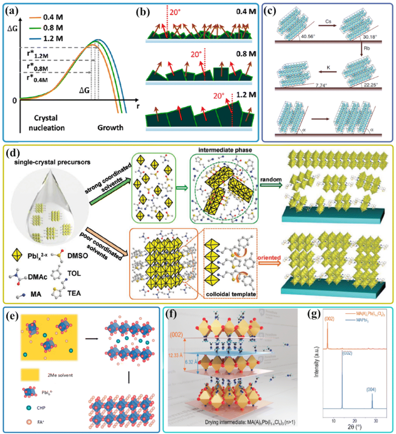 | ||
| Fig. 7 (a) Gibbs free energy plot as a function of nuclei radius. (b) Schematics of the film growth of different molar concentrations. Reproduced with permission.120 Copyright 2018, American Chemical Society. (c) The evolution schematic diagram of GIWAXS patterns occurred with cation cascade doping. Reproduced with permission.22 Copyright 2018, Nature Publishing Group. (d) Diagram showing the transformation of the colloidal phase into either random or highly oriented RPP films from single-crystal starting material in various solvents. Reproduced with permission.31 Copyright 2020, Wiley-VCH. (e) Schematic of perovskite film formation in 2Me-CHP solution. Reproduced with permission.130 Copyright 2021, Elsevier Inc. (f) Schematic illustration of the amine escaping from the lattice of the intermediate perovskite during drying and (g) XRD comparison between the final crystal and intermediate perovskites. Reproduced with permission.81 Copyright 2020, Royal Society of Chemistry. | ||
It is well known that the perovskite precursors can be regarded as a colloidal dispersion rather than a chemical solution;10 the strongly coordinating solvent DMF or DMSO would compete with A-site cations for the coordination sites around central iodoplumbates.124,125 In our previous work, we found that the size of colloidal clusters in perovskite precursors depends on the additive choice, which determines the grain size of perovskite thin films, as well as the crystal orientations.19 Besides, it was reported that the organic ions in a conventional DMF or DMF/DMSO based perovskite precursor solution are not restricted inside the PbI3− inorganic framework, resulting in the emergence of an electrical double layer made of the respective counter ions surrounding the iodoplumbates and a diffuse layer.126 Nevertheless, the single-crystal based perovskite precursor solution has been demonstrated to inherit the exceptional characteristics of the parent perovskite crystals, and fabricate the high-quality perovskite films with enhanced crystallinity, extended grain sizes, few grain boundaries and a low trap-state density.118 For example, MA+ ions are found to be captured inside the framework after the dissolution of MAPbI3 single crystals in MA gas and form the viscous liquid; the perovskite structure retains to a certain extent even on diluting the viscous liquid in a weak coordination solvent, acetonitrile (ACN). These quite different chemical species result in highly (hk0) oriented crystalline in the entire film together with the tetragonal/cubic superlattice MAPbI3 structure.127 Qin et al. devised coordination engineering of a single-crystal precursor solution in nonpolar cosolvent media.31 As shown in Fig. 7(d), instead of being solubilized and decomposing into individual ions in a cosolvent with strong coordinating abilities by allowing facile intercalation of guest DMSO molecules into the organic spacer, the single-crystal precursors in the poorly-coordinating solvents can be well kept and cause the formation of the colloidal templates, which enable 2D Ruddlesden–Popper perovskites (RPPs) to preferentially grow along the vertically ordered alignment with a narrow phase variation. A similar template strategy to induce the orientated perovskite thin films was reported by incorporating thiopheniformamidine hydrochloride (TFCl) into the perovskite precursor solution; the 1D TFPbI3 formed by reacting with MAPbI3 in the precursor solution could act as a template for the vertical growth of 3D MAPbI3 into a preferred orientation during the annealing process, which could further passivate the defects and suppress the nonradiative recombination of the MAPbI3 perovskite thin films.128
In addition to the solute and additive effect, the solvent also plays a critical role in determining the coordination of complex species in perovskite precursor solutions,125 which in turn affects the crystallization process of perovskite films, as well as the crystallographic orientations. The solvents with the high coordinating ability tend to compete with I− for the coordination sites around Pb2+ in iodoplumbate complexes, leading to retarded perovskite crystallization.125 In contrast, iodide coordination with Pb2+ dominates in the case of solvents with low coordinating ability, and thus favors iodoplumbate complex formation which is a requisite for subsequent perovskite nucleation. It is reported that only a strict control over the DMSO/DMF ratio in MAPbI3 perovskite precursor solutions enables the pure MA2Pb3I8(DMSO)2 intermediate phase, leading to the growth of perovskite films with a preferable crystal orientation along the [110] direction via the unique up-growth feature. By using strong coordination N-methyl-2-pyrrolidone (NMP) as a precursor solvent, the slow crystallization strategy in a simple one-step drop-cast method was developed to fabricate perovskite thin films with a preferred orientation at facet (004) over a growth period of 120 h.129 To meet the requirements of scalable fabrication and achieve a uniform and dense large-area perovskite thin film, it is essential to employ a solvent with a low boiling point and high vapor pressure to induce rapid nucleation of perovskites. However, such rapid nucleation causes insufficient grain growth, which lead to the formation of small perovskite grains with poor crystallinity. By a combination of Lewis bases, such as DMSO and CHP, and MACl in the perovskite precursor solutions with a volatile solvent, which can bind to the Lewis acid PbI2 and form a stable intermediate phase, the perovskite crystallization rate is retarded (Fig. 7(e)). Further crystal growth during annealing can be preferred to minimize the surface and interface energies until the complete removal of the Lewis base,130 resulting in the preferred orientation of the perovskite crystals. Recently, Wang and co-workers reported an isothermally crystallized room temperature perovskite ink for the fabrication of orientated perovskite films with an ultrahigh Lotgering factor of 97% along {00l}. The rapid solvent evaporation and spontaneous escape of the amine from the precursor reduce the interplanar distance and lead to the formation of a lower-dimensional metastable intermediate phase with a strong orientation along the [00l] direction (Fig. 7(f)). Interestingly, this highly ordered [00l] orientation could be successfully inherited by the final perovskite structure through a fast phase transition under room temperature (Fig. 7(g)).
In addition to precursor coordination engineering, regulating the status of perovskite precursor solutions also contributes to the formation of the preferred orientation of crystalline films. For example, although the introduction of tartaric acid into the Sn–Pb binary perovskite precursor solution could affect the perovskite growth dynamic by reducing the surface energy along the particular crystal planes via coordination interactions, a further ultrasonication treatment for perovskite precursor solutions for a certain time was found to induce perovskite films with a well-controlled orientation along the (224) plane, because a more uniform dispersion of coordination complexes in the perovskite precursor solutions makes it easier for perovskite grains to grow vertically along the (112) and (224) crystal planes.131 In addition, the size and dispersion of colloids in the perovskite precursor solutions have been found to continuously evolve with the solution aging time, which would have a time-dependent influence on the perovskite crystal nucleation and growth kinetics.116 As a result, highly ordered and textured perovskite thin films could be achieved after the precursor solutions aged for more than 24 h.132,133
4.2 Phase transition regulation
Halide perovskites show strong ionic characteristics with a low crystallization activation energy in the range of 56.6–97.3 kJ mol−1,3 which can be ascribed to the easy crystallization of materials. As a result, perovskite thin films with excellent crystallinity and low density of defects could be fabricated by a low-temperature solution process. However, under a spontaneous solidification process, the perovskite tends to grow as a randomly oriented polycrystal via rapid crystallization from the conventional DMSO/DMF-based precursor solution. Hence, manipulating the crystallization of the perovskite for the favorable facet orientation remains a challenge. As shown in Fig. 8(a), in our previous work, a bidentate ligand 2-aminoethanethiol (2-AET) was employed to bridge the PbI2 and MAI components in precursors; the formed PbI2·2-AET·MAI complex retards the fast crystallization of PbI2 and provides a synchronous growth environment for perovskite crystals, resulting in significantly preferred orientation along the (110) and (220) crystal planes in the perovskite thin films.134 | ||
| Fig. 8 (a) Schematic illustration of crystallographic conversion of perovskite with 2-AET during the annealing process. Reproduced with permission.134 Copyright 2016, Royal Society of Chemistry. (b) Schematic of spontaneous structural conversion from the 2D MAFAPbI3Cl perovskite intermediate to the (111) uniaxial oriented 3D α-FAPbI3 perovskite. Reproduced with permission.163 Copyright 2019, Elsevier Inc. The total Gibbs free energy as a function of r without seed (c) and with seed (d). (e) Pole figure measurements along the (002) facet orientation with different seed concentrations. Control, 0.3 mol% and 0.6 mol%. Reproduced with permission.21 Copyright 2022, Elsevier Inc. (f) The top-view SEM image of PCA. Scale bar, 10 μm. (g) XRD pattern of PCA and the final perovskite film. Reproduced with permission.167 Copyright 2022, Royal Society of Chemistry. | ||
In fact, a diverse range of additives containing organic cations and halide anions have been deliberately incorporated into perovskite precursors (Table 1).38,135–137 These additive strategies often require multiple phase transition steps to yield the pure perovskite phase, in which the residual solvent and additive molecules remaining within the wet films are expected to modulate subsequent perovskite crystallization by forming perovskite–solvent chelated intermediates and perovskite–additive intermediates. Then the additive would be gradually driven to the grain boundaries and increase surface and interface energies, which contribute to the thermodynamic driving force on the growth of the perovskite crystals.38 This extra crystal growth favors the formation of perovskite thin films with preferred crystal orientation. For example, the incorporation of tetrahydrothiophene oxide into the MAPbI3 precursor solution was reported to have strong interaction with MAPbI3 precursors and suppresses homogeneous nuclei and crystalline intermediate structures; heterogeneous nucleation at the interface enable the growth of the perovskite thin film with a strong tetragonal (100) crystallographic orientation.28 In addition to 3D perovskites, a great number of additives, such as KI,138 NH4SCN,139,140 MACl,141 NH4Cl,142,143 thiourea,144 and MASCN,145 have been also demonstrated to align the 2D perovskite layers perpendicular to the substrate and control the growth orientation, thus achieving desirable vertically oriented 2D perovskite thin films with improved crystallinity. In a very recent study, pseudohalide additives, such as methylammonium thiocyanate (MASCN), were reported to induce the conversion of a low-n to a high-n phase distribution in 2D perovskite thin films, leading to the growth of high-quality and oriented large-grain perovskite thin films, which facilitates to improve the crystalline quality, decrease the lattice defect, and reduce the nonradiative recombination.145
| Perovskite composition | Additive | Orientation plane | YearRef. |
|---|---|---|---|
| MAPbI3 | PbCl2 | (110) | 2015146 |
| MAPbI3 | Methylammonium chloride | (110) | 2016147 |
| MAPbI3 | 2-Aminoethanethiol | (110) | 2016134 |
| MAPbI3 | Methylammonium acetate and thio-semicarbazide | (110) | 2017148 |
| MAPbI3 | Thiourea | (110) | 2017149 |
| MAPbI3 | Methylammonium thiocyanate (MASCN) | (110) | 2017150 |
| MAPbI3 | Tetrahydrothiophene oxide | (100) | 201728 |
| MAPbI3 | Methylamine gas | (hk0) | 2020127,151 |
| FAPbI3 | Alkylamine iodine | (001) | 2021152 |
| CsPbBr3 | HBr | (121) | 202083 |
| FA0.8Cs0.2Pb(I0.7Br0.3)3 | Pb(SCN)2 | (101) | 2017153 |
| FA0.83Cs0.17Pb(I0.8Br0.2)3 | Hydrohalic acids | (100) | 2017132 |
| Rb0.05Cs0.05(FA1−xMAx)Pb(I1−xBrx)3 | 4-(2-Aminoethyl)-benzenesulfonyl fluoride hydrochloride benzenesulfonyl fluoride hydrochloride | (100) | 2022154 |
| Cs0.2FA0.8Pb(I0.7Br0.3)3 | 4-Fluoro-phenylethylammonium iodide iodide | (100) | 2022155 |
| (BA)2(MA)n−1PbnI3n+1 | NH4SCN | (111) | 2018140 |
| (BA)2(MA)n−1PbnI3n+1 | Thiourea | (111) | 2018144 |
| BA2MA3Pb4I13 | KI | (001) | 2019138 |
| (PEA)2(MA)n−1PbnI3n+1 | NH4SCN | (101) | 2018139 |
| (PEA)2(MA)4Pb5I16 | NH4SCN and NH4Cl | (111) | 2018142 |
| (PEA)2(MA)4Pb5I13 | NH4Cl and DMSO | (101) | 2019143 |
| (PEA)2(MA)4Pb5I16 | MACl | (111) | 2020141 |
| (PA)2(MA)4Pb5I16 | MASCN | (011) | 2022145 |
To date, most of the record PSCs contain MACl as the additive to suppress the fast phase transition and achieve controlled growth of perovskite thin films along with certain orientations;156–159 these chloride-derived perovskite thin films possess highly preferred orientation parallel to the substrate.19,147,160–162 Zhang et al. reported a low-temperature fabrication of the uniaxial-oriented α-FAPbI3 film induced by a metastable 2D MAFAPbI3Cl perovskite intermediate phase.163 As shown in Fig. 8(b), In the case of a designed precursor solution with a stoichiometric ratio of MA![[thin space (1/6-em)]](https://www.rsc.org/images/entities/char_2009.gif) :FA:Pb:I:Cl = 1:1:1:3:1 using either MAI + PbI2 + FACl or FAI + PbI2 + MACl precursors, colloidal [PbI3Cl]2− nanosheet with FA+ and MA+ cations in precursor solution would be forcedly extracted by anti-solvent during film formation, and form the metastable 2D MAFAPbI3Cl perovskite intermediate phase, in which the structure with cross-distribution of Cl at the bilateral anion sites is energetically favored. Then both the I/Cl anions and MA/FA cations exchange leads to the 45° tilt of the lattice, which is responsible for the (111) oriented growth of α-FAPbI3 at room temperature. Further annealing treatment significantly enhances film quality accompanied by the removal of MACl; a high-quality (111) oriented α-FAPbI3 film is formed. It is worth noting that the driving force for forming such a metastable 2D MAFAPbI3Cl intermediate phase is solvent extraction, and phase-pure α-FAPbI3 can be obtained after anti-solvent extraction.
:FA:Pb:I:Cl = 1:1:1:3:1 using either MAI + PbI2 + FACl or FAI + PbI2 + MACl precursors, colloidal [PbI3Cl]2− nanosheet with FA+ and MA+ cations in precursor solution would be forcedly extracted by anti-solvent during film formation, and form the metastable 2D MAFAPbI3Cl perovskite intermediate phase, in which the structure with cross-distribution of Cl at the bilateral anion sites is energetically favored. Then both the I/Cl anions and MA/FA cations exchange leads to the 45° tilt of the lattice, which is responsible for the (111) oriented growth of α-FAPbI3 at room temperature. Further annealing treatment significantly enhances film quality accompanied by the removal of MACl; a high-quality (111) oriented α-FAPbI3 film is formed. It is worth noting that the driving force for forming such a metastable 2D MAFAPbI3Cl intermediate phase is solvent extraction, and phase-pure α-FAPbI3 can be obtained after anti-solvent extraction.
In the last few years, the perovskite seed-assisted growth method has been developed to facilitate crystallization during the formation of the perovskite.164–166 For example, the highly oriented 2D Dion–Jacobson (DJ) phase perovskites (BDA)PbI4 (BDA is 1,4-butanediamine) were reported as seeds to optimize the growth kinetics of a 3D perovskite in a two-step solution processed method.21 Since the large seed crystals (more than 300 nm) could directly serve as growth centers, the nucleation stage of perovskite is not required (Fig. 8(c and d)); this seed-induced crystallization could achieve the heteroepitaxial growth of 3D perovskites with highly (001) and (002) facet orientations (Fig. 8(e)). Besides, the 2D seeds were found to transform into the perovskite grain boundary to passivate the grain boundary, inhibit ion migration, and improve the stability. In a very recent study, the as-prepared patterned perovskite crystal array regularly distributing on the substrate served as templated crystals to induce the bottom-up crystallization of perovskites in the subsequent solution process (Fig. 8(f)).167 Note that the PbI2 layer was evaporated on the perovskite crystal array to avoid dissolution. As shown in Fig. 8(g), the orientation of the PCA crystal is the same as that of the final perovskite film.
4.3 Deposition condition optimization
Annealing is an essential process in the solution-processed perovskite thin films; various strategies have been developed to modify the annealing procedure. Specifically, rapid thermal annealing methods have been successfully developed to control perovskite crystallization and to scale up perovskite solar cells with a highly crystalline phase-continuous film.168,169 For example, a spherulitic growth behavior has been reported to obtain highly orientated MAPbI3 perovskite grains along with both the (112) and (400) planes with tens of micrometers in size via flash infrared annealing (FIRA), which may be driven by the strain induced by the difference in the thermal expansion coefficient between the perovskite and the substrate during the cooling process (Fig. 9(a)).32 A similar annealing temperature-induced crystal orientation of the MAPbI3 thin film was reported in an electrospray deposition technique, where the (002) orientation is preferred at room temperature, then the (110) direction starts to rise and becomes dominant at a high temperature.170 Interestingly, further introducing a thermal gradient on the growth substrate through local heating could control the macroscopic solidification direction and confine perovskite crystal orientations. As shown in Fig. 9(b and c), by balancing both temperature and concentration, this method allows growing well-aligned perovskite films with periodic microarrays over several square centimeters, which mainly orient along the unique (112) or (200) directions parallel to the substrate (Fig. 9(d)).87 This suggests that perovskite crystal orientation could be obtained via precise control of the process conditions. Note that an ionic liquid of methylammonium formate (MAFa) was employed as a solvent to afford the sharp liquid-to-crystalline solid transition of MAPbI3, rather than generating plumbate intermediates during perovskite crystallization. Moreover, MAFa has excellent solubility in both PbI2 and MAI; this enables the efficient intercalation process of MA cations into the lead halide crystal frameworks, which rearrange the initial PbI6 octahedral crystals and reduce the surface energy via Ostwald ripening during thermal annealing. | ||
| Fig. 9 (a). Schematic spherulitic growth of perovskite films after 0.2, 0.5, 1, and 1.2 s of FIRA annealing. Reproduced with permission.32 Copyright 2019, American Chemical Society. (b). Schematic representation of the thermal-gradient-assisted directional crystallization process of a MAPbI3 perovskite. (c) Optical microscope image of the aligned OPC films of the perovskite. (d) Unit cell of the tetragonal MAPbI3 perovskite showing (112) and (200) planes. Reproduced with permission.87 Copyright 2016, Nature Publishing Group. (e) Scanning electron microscopy (SEM) image of single-crystal perovskite patterned thin film consisting of 10 μm-wide strips with 400 nm-wide spacing. (f) Cross-sectional SEM image of 200 nm-thick perovskite single-crystal strips, showing sharp edges and smooth morphology. (g) Two-dimensional X-ray diffraction (2D XRD) image of single crystal perovskite patterned thin films prepared by the geometrically confined lateral crystal growth (GC-LCG) process using a line-patterned mold consisting of 10 μm-wide and 200 nm-thick strips with 400 nm-wide spacing. (h) Out-of-plane XRD scan of the single-crystal perovskite patterned thin film. Diffraction peaks are consistent with the diffraction spots along the qz line obtained by 2D XRD. (i) In-plane f scan of single-crystal perovskite patterned thin film obtained at the fixed 2θ angle of the (002) plane. Reproduced with permission.171 Copyright 2017, Nature Publishing Group. (j) Schematic of the compression process on the perovskite film with nanoimprinting stamps. Reproduced with permission.33 Copyright 2018, Wiley-VCH. (k) Schematics of the crystallization mechanism for cold antisolvent temperature conditions, a small number of nuclei were formed by heterogeneous nucleation, owing to the high Gibbs free energy of nucleation. (l) XRD pattern of the cold and ambient antisolvent-bathed MAPbI3 perovskite deposited on ITO after annealing. Reproduced with permission.173 Copyright 2019, Wiley-VCH. | ||
By combining the hot-casting technique and lateral crystal growth, Lee et al. developed a facile roll-printing method to fabricate large-scale, single-crystal MAPbI3 perovskite thin films.171 A cylindrical metal roller is wrapped with a flexible poly(dimethylsiloxane) (PDMS) mold that has a periodic array of wide and shallow channels, which provides geometrical confinement to prevent the crystal growth in the vertical direction (Fig. 9(e–h)). Meanwhile, the perovskite ink solution filled in the channels is crystallized instantly with immediate solvent evaporation caused by the hot substrate (180 °C). At an optimal mold rolling speed, nanometre-sized MAPbI3 arrays with identical widths and equally narrow spaces can be grown. The sharp and strong reflection spots in the 2D X-ray diffraction image clearly indicate that the film has a single-crystal nature, Fig. 8(g). Besides, as shown in Fig. 9(h–i), there are only two diffraction peaks of (110) and (220) planes in the out-of-plane X-ray diffraction pattern, and the four sharp peaks appear every 90° in the in-plane phi scan; these results confirm the formation of a highly ordered fourfold symmetry of the tetragonal perovskite single-crystal of MAPbI3.
In addition to hot-casting assisted perovskite crystallization, a facile pressure-induced highly orientated perovskite thin film with low-angle grain boundaries was reported (Fig. 9(j)).33 The hexagonal nanodot array PUA stamp with a diameter of 250 nm can provide a large effective stress ranging from 140.1 to 231.3 kPa in a partially dried perovskite intermediate film, which could accelerate the densification of the perovskite film and improve the crystallinity. Meanwhile, the perovskite grains could grow in a specific direction due to the z-directional compressive stresses in a geometry-defined space, leading to the formation of highly oriented perovskite thin films.
Considering the low critical Gibbs free energy of perovskite nucleation (called self-assembly), a large number of nuclei and random orientation lead to perovskite thin films without preferential orientations.172 In this regard, a facile cold antisolvent bathing approach was reported to allow the growth of highly oriented perovskites along the [110] and [220] directions (Fig. 9(k and l)), which could retard the nucleation and growth kinetics and prolong the time to find energetically favored growing planes.173
4.4 Epitaxial growth
Since the interface of the film with the substrate plays an important role in grain growth, epitaxial growth has been demonstrated as a powerful technique in the fabrication of high-quality semiconductor films with preferential orientation on the crystalline seed layer. For example, the formation of crystallographic texture was reported in CsPbI3 thin films, in which perovskite–substrate interface ‘‘pins’’ the initial anisotropic cubic CsPbI3 unit cell at high temperature, then undergoes tensile strain and texture formation upon cooling, leading to a relative lattice reduction out-of-plane.47,174 As shown in Fig. 10(a), considering a very low lattice mismatch factor between two unit cells of CsPbBr3 and three unit cells of SrTiO3 along both CsPbBr3[100]‖SrTiO3[100] and CsPbBr3[010]‖SrTiO3[010] directions, vapor-phase epitaxial growth of CsPbBr3 single-crystal thin films was achieved via heteroepitaxial growth on SrTiO3.175 It is worth noting that continuous CsPbBr3 single-crystal thin films could be obtained at a high reaction temperature of 450 °C as the enhanced diffusion of the adatoms increases the nucleation density and avoids randomly grown irregular nanostructures. There are only (100) and (200) diffraction peaks observed on the PXRD pattern as shown in Fig. 10(b); the lack of other diffraction peaks indicates the single crystalline quality of CsPbBr3 thin films.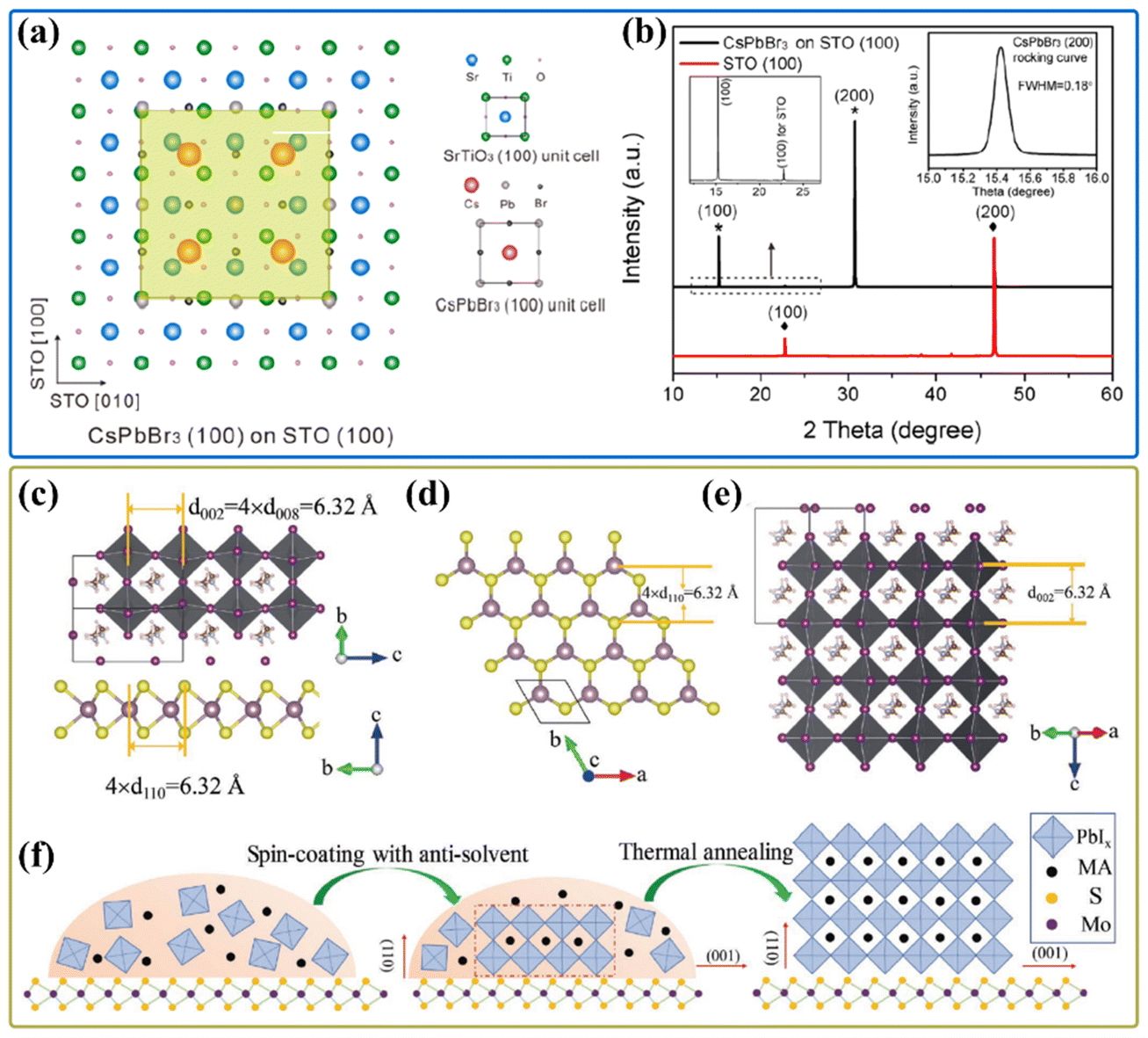 | ||
| Fig. 10 (a) Illustration of the incommensurate lattice match between CsPbBr3 (100) and STO (100) crystallographic planes. (b) PXRD patterns of the CsPbBr3 nanostructures grown on STO (100) and STO (110) substrates. Inset is the magnified range of 13°–32° for the CsPbBr3/STO (100) sample. Reproduced with permission.175 Copyright 2017, American Chemical Society. (c) The side view of atomic crystal heterojunction of MAPbI3 and MoS2. (d and e) Atomic crystal structure of the (001) plane of MoS2 (d) and the (110) plane of the perovskite (e). (f) Schematic diagram of the vdW epitaxial growth of a MAPbI3 grain on a MoS2 surface. Reproduced with permission.34 Copyright 2019, Wiley-VCH. | ||
The weak van der Waals interactions between the substrate and the grown material with an inactive surface result in a small lattice-mismatch distortion in the grown film even in the presence of different lattice constants or crystal structures between them. Tang et al. developed the solution-phase van der Waals epitaxial growth of MAPbI3 perovskite on MoS2 flakes.34 Considering the identical interplane distances of (008) and MoS2 (110) planes (1.58 Å), the in-plane coupling between MoS2 and MAPbI3 enables the growth of MAPbI3 grains on the surface of MoS2 templates, Fig. 10(c–e). Besides, the dangling-bond-free surface of MoS2 facilitates the migration of atoms and further accelerates the perovskite growth along the lateral direction, leading to the out-of-plane orientation of the perovskite layers along (110) (Fig. 10(f)). Recently, a similar van der Waals epitaxial growth strategy was also reported for all-inorganic CsPbIBr2; enhanced preferential orientation of CsPbIBr2 could be obtained on the substrate modification with MoS2 flakes.176
4.5 Post treatment
Excellent progress has been made on the post-treatment of perovskite thin films to passivate the defects of the interface and grain boundary.65,177–180 Several research groups have demonstrated the fabrication of high-quality perovskite thin films with the desired microstructure through post-processing morphology-reconstruction owing to their ‘soft’ lattices. For example, a solvent annealing strategy has been successfully developed to promote the precipitation and crystallization of lead halide and assist the diffusion of organic cations and halide anions, leading to the formation of uniformly distributed perovskite nuclei.29 These uniform perovskite nuclei could be further rearranged and coalesced via the Ostwald ripening process during the annealing process, which facilitates the transformation of crystal orientation into the (h00) orientation. Except for the wet perovskite thin films (without annealing), MAPbI3 crystal was reported to melt into the metastable liquid intermediate phase of MAPbI3·(x)MA upon exposure to the MA gas.16 Then the liquid MAPbI3·(x)MA phase begins to recrystallize within 2 min after the removal of the MA gas, and the perovskite thin films with higher degree of crystallinity and texture could be obtained. However, the process is difficult to control and is dominated by the nucleation process; the massive nuclei formed from the saturated liquid result in the formation of small perovskite grains. The following study confirmed that the degree of the supersaturation of the liquid phase was strongly dependent on the release rate of the MA gas; the slower the release of the MA gas from the liquid phase, the larger the grain size in perovskite thin films.44 As a result, the perovskite film with (110)-uniaxial crystallographic orientation with millimeter-sized grains could be obtained at a certain partial pressure of the MA gas (Fig. 11(a)). More importantly, as confirmed by the EBSD results in Fig. 11(b and c), there is the same crystallographic orientation for each grain in an area of 1.75 × 1.21 mm2.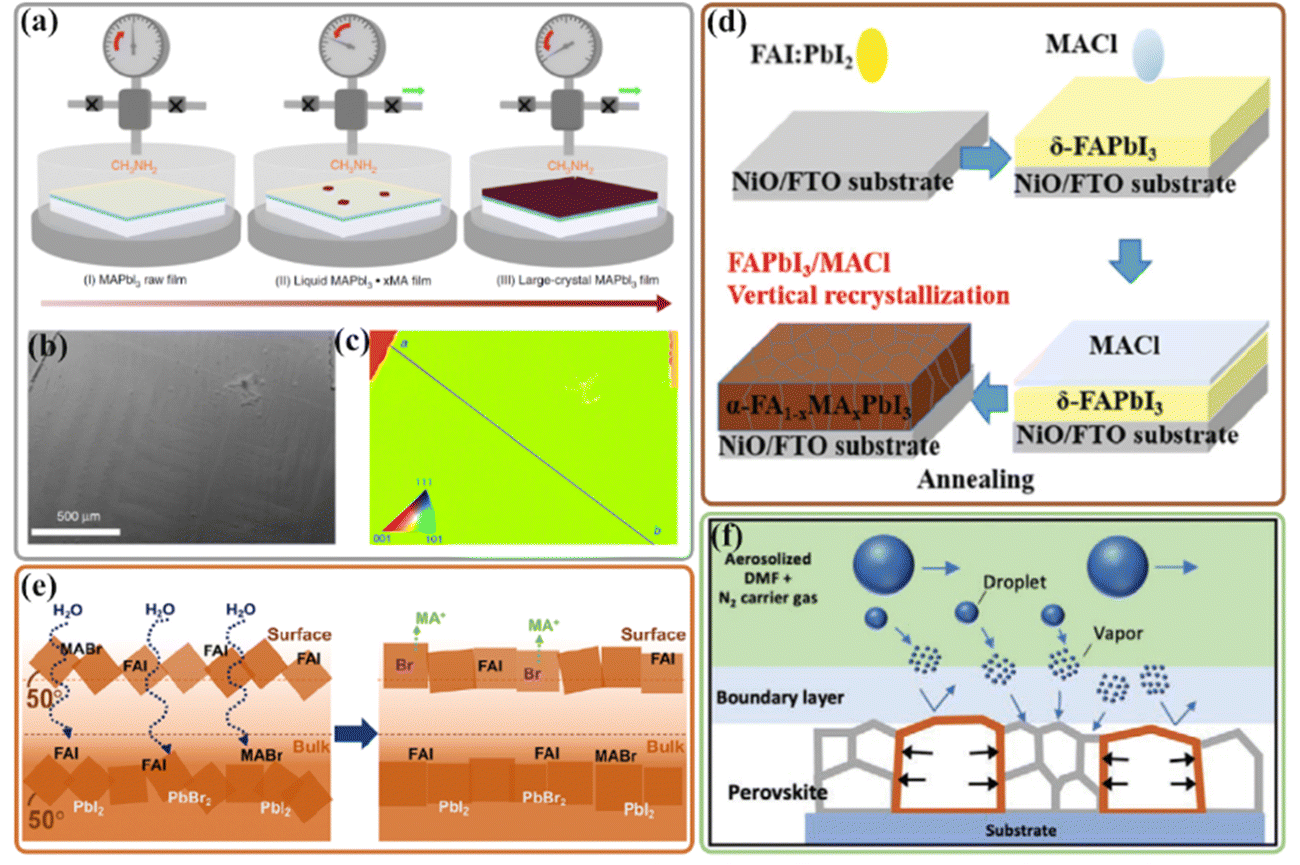 | ||
| Fig. 11 (a) The steps of the method: (I) formation of a liquid MAPbI3·xMA intermediate film; (II) controlled growth of the nuclei; and (III) controlled growth of the perovskite film. (b) Backscattered electron (BSE) image. (c) X axis inverse pole figure (IPF) (parallel to the sample surface). Reproduced with permission.44 Copyright 2020, Nature Publishing Group. (d) Illustration of the vertical recrystallization method for the formation of a high-quality FAPbI3/MACl film. Reproduced with permission.183 Copyright 2017, N Royal Society of Chemistry. (e) Illustration of the proposed moisture diffusion mechanism due to exposure to moisture. Reproduced with permission.113 Copyright 2020, American Chemical Society. (f) Schematic drawing showing solvent vapor diffusion through the boundary layer resulting in the preferential consumption of small grains and the subsequent growth of the larger grains, while condensation of solvent droplets is prevented. Reproduced with permission.185 Copyright 2021, Wiley-VCH. | ||
It is well known that FA-based perovskites suffer from phase transition to a yellow non-perovskite phase (δ-FAPbI3) at room temperature;181,182 a vertical recrystallization was reported to prepare α-phase FAPbI3 perovskite films with high crystallinity.183 As shown in Fig. 11(d), by deposition of a certain amount of MACl on the pre-deposited yellow δ-phase FAPbI3 film, the vertical diffusion of MACl into the δ-phase FAPbI3 thin films triggers the phase transformation to black α-phase FAPbI3, yielding the desirable highly recrystallized perovskite film. A similar study with respect to a surface-induced secondary grain growth technique was reported, in which the decrease in the surface energy of a crystal facet induced by organic ammoniums provides the driving force for secondary grain growth, leading to the grain boundaries’ rearrangement along the orientation to minimize the free energy of the system. As a result, enlarged grain sizes of up to 4 μm with a more preferred out-of-plane orientation in the entire CsPbI2Br perovskite thin film could be achieved.35
Although the perovskite is notoriously sensitive to moisture and undergoes decomposition by releasing organic components,134 exposing perovskite thin films to moisture for the short time has been reported to enhance the microscale film morphology and change the crystallographic orientation.113,184 As shown in Fig. 11(e), excess organics present at the surface of perovskite thin films have strong interactions with water that allow for greater diffusion throughout the entirety of the films, thus leading to the rearrangement of the crystallographic texture in the (001) plane, which contribute to the enhancement of photocurrents and long-term device stability.113
In addition to the moisture-induced rearrangement of the crystallographic texture, a scalable aerosol treatment method has been reported to enhance the grain size and crystallinity of perovskite thin films.185 The aerosol containing DMF droplets was transported to the surface of perovskite thin film and promoted inter-grain mass transport. As a result, the grain boundaries are prone to move from the large grain side to the small grain side to minimize the grain surface energy; the growth of large grains occurs by the consumption of small grains via an Ostwald ripening process (Fig. 11(f)). By optimizing the processing parameters involving temperature, flow rate, and treatment time, the perovskite thin films with a preferential (110) crystallographic orientation could be achieved.
5. Crystal orientation-dependent photovoltaic performance of PSCs
In Section 3, we have discussed the crystal orientation-dependent optoelectronic properties of halide perovskites; it is no doubt that tailoring the perovskite crystal facet with specific orientation is an effective approach to provide a higher carrier mobility, desired interfacial energy alignment, and a lower trap state density. In this regard, high crystalline orientation and large grain sizes of perovskite thin films could notably eliminate the density of grain boundaries and decrease carrier recombination, which would be beneficial to breaking through the bottleneck on perovskite solar cell photovoltaic performance. However, considering the fact that many high efficiencies of PSCs over 20% in the literature are based on small perovskite grains without obvious crystal orientation, the debate with respect to the impact of crystallographic orientation of perovskite thin films on the macroscopic performance of PSCs is still ongoing. It was reported that although there is a strong crystallographic orientation in the flash infrared annealing (FIRA) induced MAPbI3 thin films, comparable optoelectronic properties such as local PL emission intensity, charge carrier lifetimes, and mobilities could be observed between these thin films and conventional case, suggesting that the optoelectronic quality is not necessarily related to the orientation and size of crystalline domains.32 Nevertheless, a few theoretical calculation studies have investigated the crystal anisotropy effect on the performance of PSCs. The first-principle calculations and drift-diffusion model suggest that the optoelectronic performance of tetragonal MAPbI3 along the [001] direction is superior to that along the [100] direction, a PCE of 25.45% can be achieved for the single-junction perovskite solar cells based on MAPbI3 along the [001] direction, compared to that of 21.77% in the [100] direction.23 A similar crystal anisotropy effect is also explored for inorganic CsPbIxBr3−x. Due to the superior optical and transport characters and the larger difference of the perovskite layer quasi Fermi levels along the [001] orientation, the device performances, including PCE, short-circuit current density, and open-circuit voltage, of CsPbIxBr3−x PSCs along the [001] orientation are enhanced than those along [100].186 In addition, as summarized in Table 2, the experimental effort in the crystal orientation-dependent photovoltaic performance of PSCs based on diverse perovskite compositions has been widely demonstrated, suggesting that deliberately promoting the favorable facet orientations of perovskite is also a potential strategy to further boost the efficiency of PSCs based on both 3D and 2D perovskite thin films. For example, Giesbrecht et al. established the correlation between morphology and crystal orientation of bromide-based perovskite thin films and solar cell performance via a controlled solvent drying method.187 To discriminate whether the crystal size or the crystal orientation is the dominant factor determining the photovoltaic performance, they found that the rougher bottom contact on fluorine-doped tin oxide (FTO) substrate limits the horizontal perovskite growth. More importantly, a high degree of orientation with the (001) plane parallel to the substrate could be retained regardless of the crystal size, making it reasonable to confirm that the short-circuit current is affected by the degree of crystal order in the film. In this regard, controlling the crystal orientation will further improve the efficiency of PSCs.| Perovskite composition | Orientation plane | Method | PCE (%) | YearRef. |
|---|---|---|---|---|
| MAPbI3 | (110) | Additive strategy | 9.32 | 2015188 |
| MAPbI3 | (110) | Additive strategy | 12.0 | 2015189 |
| MAPbI3 | (h00) | Solvent annealing | 12.38 | 201629 |
| MAPbI3 | (004) | Precursor engineering | 15.0 | 2017129 |
| MAPbI3 | (110) | Additive strategy | 18.46 | 2017149 |
| MAPbI3 | (110) | Pressure-induced crystallization | 19.16 | 201733 |
| MAPbI3 | (110) | Epitaxial growth | 20.55 | 201934 |
| MAPbI3 | (110) | Methylamine-assisted growth | 21.36 | 202044 |
| MAPbI3 | (110) | Precursor engineering | 19.69 | 2021162 |
| MAPbI3 | (200) | Hot-casting | 20.22 | 2022190 |
| MAPb(I1−xClx)3 | (002) | Isothermally crystallizing | 23.1 | 202081 |
| MAPbBr3 | (001) | Controlled solvent drying | 6.08 | 2016187 |
| FAPbI3 | — | Additive strategy | 13.6 | 2016191 |
| FAPbI3 | (110) | Additive strategy | 17.0 | 2016192 |
| FAPbI3 | (110) | Post-growth treatment | 20.65 | 2017183 |
| FA0.6MA0.4PbI(3−y)Cly | (11) |
Topotactic-oriented attachment | 19.7 | 201724 |
| (FAMACsRbPbI3)0.85(MAPbBr3)0.15 | (001) | Composition engineering | 20.99 | 201822 |
| FA1−xMAxPbI2.87Br0.13 | (001) | Composition engineering | 21.21 | 2019122 |
| FA0.75MA0.25PbI3 | (001) | Seed-induced growth | 23.95 | 202221 |
| Cs0.05(MA0.17FA0.83)0.95Pb(I0.83Br0.17)3 | (001) | Moisture exposure | 18.0 | 2020113 |
| (PEA)2(MA)4Pb5I16 | (101) | Additive strategy | 11.01 | 2018139 |
| (TEA)2(MA)2Pb3I10 | (111) | Precursor engineering | 14.68 | 202031 |
| (BDA)(MA)4Pb5I16 | (011) | Additive strategy | 18.72 | 2022145 |
As mentioned in Section 3.2, controlling the crystalline orientation in polycrystalline thin films can enhance charge transport within the bulk by reducing the structural disorder. A 300% higher carrier mobility in the (11) uniaxial-oriented TOA perovskite thin film has been demonstrated to improve the efficiency of TOA-PSCs, and significantly reduce the hysteresis.24 A similar improvement in PCE was reported for the highly orientated MAPbI3 thin film with the long range order in the millimeter scale, which was prepared by combining anti-solvent engineering (induce rapid crystallite precipitation), gas blowing (orientates the grains and brings them closer), and H2O post-treatment (grain boundary mending). The high conductivity within these perovskite grains yields a PCE of 21.06% with an impressive fill factor value of 86% for the corresponding PSCs.193
In addition to the enhancement of carrier mobility, the crystal orientation in perovskite thin films could change interfacial energy alignments and charge density redistributions, which is expected to reduce the energy barrier between the perovskite and the charge transporting layer and improve the photovoltaic efficiency of devices. As discussed in Section 3.1, although both MAPbI3 thin films with (001) and (100) planes favor hole transfer to the hole transport layer, the PL intensity of the MAPbI3 single-crystal films with (001) surface orientations was found to increase upon depositing phenyl-C61-butyric acid methyl ester (PCBM) as an electron transport layer, while the charge carrier transfer efficiency estimated from PL intensity is 51.6% in the case of MAPbI3 (100), indicating that efficient electron transfer to the electron transport layer occurs only from the MAPbI3 thin films with the (100) surface orientations.20 As a result, a higher efficiency of 19.3% was achieved for the PSCs based on MAPbI3 (100) single crystal film, compared to the PCE of 16.0% for that of the MAPbI3 (001) case (Fig. 12(a–d)). These successes confirm the potential of perovskite crystallization and preferred orientations to improve the charge transfer properties at the charge transport layer/perovskite interfaces and enhance the photovoltaic performance of PSCs.
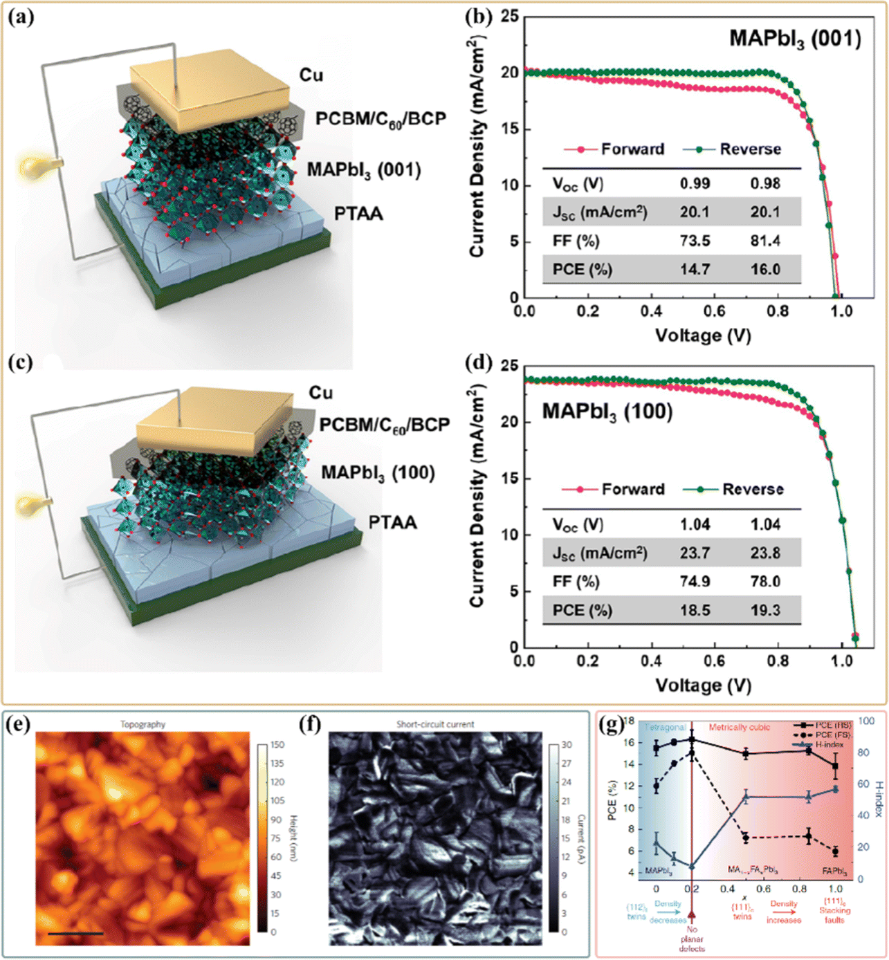 | ||
| Fig. 12 (a and c) Schematic diagram of the MAPbI3 (001) and MAPbI3 (100) single-crystal film solar cells. (b and d) J–V curves of the solar cells obtained in forward-scan (red) and reverse-scan (green) modes measured in a nitrogen-filled glovebox. Reproduced with permission.20 Copyright 2022, American Chemical Society. (e) Topography image corresponding to all current maps. Individual crystal grains and their facets are clearly visible. The scale bar is 500 nm. (f) ISC map measured at 0 V bias under illumination. Reproduced with permission.26 Copyright 2016, Nature Publishing Group. (g) The average PCEs calculated from the reverse and forward scans, and the corresponding H-indices as a function of x in the MA1−xFAxPbI3 compounds studied. Reproduced with permission.27 Copyright 2021, Nature Publishing Group. | ||
Besides, several studies have tried to directly link the facet-dependent density of trap states in perovskite thin films with macroscopic PCE of the related PSCs. The topography image in Fig. 12(e) shows that there are various crystal facets within individual crystal grains,26 which is consistent with the EBSD results as discussed in Section 3.3. Meanwhile, the heterogeneity of Isc is not only observed among individual grains but also in intra-grain. Isc varies by up to an order of magnitude within individual grains, and the average Isc for these grains does not relate to the grain size (Fig. 12(f)). Voc values show similar intra-grain heterogeneity as in the case of Isc. Considering the fact that the presence of spatial variations in PL intensity and lifetime between different grains, due to changes in trap state concentrations,194 the authors hypothesized that the origin of these local heterogeneity in Isc and Voc is a consequence of facet-dependent density of trap states in perovskite thin films, which is expected to have a direct effect on macroscale solar cell performance. In a recent study, PSC performance in different MA1−xFAxPbI3 compositions was explored, in which the type and density of the intragrain planar defects change with the MA/FA ratio.27 In the case of MAPbI3 (x = 0), almost all the grains are twinned with {112} boundaries, then nearly half of the grains show{112} twin domains for tetragonal MA1−xFAxPbI3 (0 < x < 0.2), Fig. 12(g). Note that no twinned reflections were observed in MA0.8FA0.2PbI3 grains, and the lattice transform to the metrically cubic lattice. Once the FA content is more than 50%, there is a different type of twinning with {111} boundaries or stacking faults within a cubic MA1−xFAxPbI3 lattice, and a higher stacking fault density was observed for FAPbI3 (x = 1). As a result, PCE deteriorates with increasing density of both types of intragrain planar defects, depending on the FA/MA ratio in MA1−xFAxPbI3. The planar-defect-free MA0.8FA0.2PbI3 based PSCs show the highest PCE in both the reverse and forward scans, whereas FAPbI3 shows the poorest performance. These results will offer further scope for a systematic optimization of perovskite crystal orientation to develop high-performance PSCs.
6. Conclusions and outlook
In summary, we have systematically reviewed the crystal orientation-dependent optoelectronic properties of halide perovskites with the consideration of their influence on the photovoltaic performance of PSCs, as well as the basic strategies and oriented growth mechanisms for crystal orientation engineering in the fabrication of preferentially oriented perovskite thin films. Due to various atomic arrangements and coordination along with different orientations, the preferential orientation of perovskite thin films plays a vital role in fine-tuning the properties of perovskites, especially the surface properties, charge transfer properties, interfacial energy alignment, trap states, and lattice strain. Although there is still a debate regarding the impact of the crystallographic orientation of perovskite thin films on the macroscopic performance of PSCs, the success in both theoretical and experimental studies has revealed that manipulating perovskite crystal orientation could provide great potential for further breaking through the bottleneck of PSCs’ photovoltaic performance. To date, crystal orientation engineering has been successfully adopted to allow the preferential growth orientation of perovskite thin films along some certain crystal planes, in which facet orientation tailoring and facet stack optimization require efforts to precisely control nucleation and optimize growth conditions. However, challenges in controlling the crystallographic orientations of perovskite thin films still need to be addressed.(1) Due to the ionic characteristics and low crystallization activation energies of halide perovskites, it is usually difficult to tailor the specific facet orientations and stack of the perovskite thin films, or at least inhibit some undesired facet orientations to reduce disordered electronic states and improve the charge transport properties. The preferential growth orientation of perovskite thin films for most of the approaches strongly depends on their initial orientations, and the tetragonal MAPbI3 tends to retain the (110) and (220) crystal planes, whereas it is easier to retain the (100) and (200) crystal planes in the cubic FAPbI3. One could expect that the enhanced orientations along these initial orientations in perovskite thin films may limit their potential to exhibit a superior optoelectronic performance.
(2) The presence of grain boundaries and intragrain planar defects, such as misorientation, degree of disorder, twin boundaries and stacking faults has been demonstrated to introduce defects and deteriorate the PSC performance.18,66 Considering the neighboring grains that connect with each other in a particular orientation in the case of preferentially orientated crystals, efforts to grow large and oriented perovskite grains with small angle grain boundaries would efficiently reduce local crystal misorientation between neighboring grains and sub-grains, which is essential for reducing the generation of defects at the grain boundaries as well as local strain in halide perovskite films, thus leading to more efficient PSCs.
(3) The residual additive incorporated in precursor engineering, phase transition regulation and post-treatment strategies for grain boundaries or within the perovskite could passivate the defects, which also improve the optoelectronic performance of perovskite thin films, resulting in a higher carrier mobility and a lower density of trap states. There is a lack of reliable and effective strategy to evaluate the contribution of crystal orientation for the improvement of optoelectronic performance in perovskite thin films. Hence, developing single crystal perovskite thin films with different orientations or epitaxial growth of oriented perovskite thin films is expected to provide direct guidance for the role of crystal orientation in modulating the charge transport properties, the trap state density, and the lattice strain.
Conflicts of interest
There are no conflicts of interest to declare.Acknowledgements
The authors thank Prof. Anders Hagfeldt for the initial contributions to this review article. This work was supported by Key Science and Technology Innovation Team of Shaanxi Province (2022TD-34).References
- A. K. K. T. Y. S. T. Miyasaka, Organometal Halide Perovskites as Visible-Light Sensitizers for Photovoltaic Cells, J. Am. Chem. Soc., 2009, 131(17), 6050–6051 CrossRef PubMed.
- National renewable energy laboratory, best research-cell efficiency chart. https://www.nrel.gov/pv/assets/images/efficiency-chart.png, accessed: June 2022 Search PubMed.
- D. T. Moore, H. Sai, K. W. Tan, D. M. Smilgies, W. Zhang, H. J. Snaith, U. Wiesner and L. A. Estroff, Crystallization kinetics of organic-inorganic trihalide perovskites and the role of the lead anion in crystal growth, J. Am. Chem. Soc., 2015, 137(6), 2350–2358 CrossRef CAS PubMed.
- N. J. Jeon, J. H. Noh, Y. C. Kim, W. S. Yang, S. Ryu and S. I. Seok, Solvent engineering for high-performance inorganic-organic hybrid perovskite solar cells, Nat. Mater., 2014, 13(9), 897–903 CrossRef CAS PubMed.
- M. Xiao, F. Huang, W. Huang, Y. Dkhissi, Y. Zhu, J. Etheridge, A. Gray-Weale, U. Bach, Y. B. Cheng and L. Spiccia, A fast deposition-crystallization procedure for highly efficient lead iodide perovskite thin-film solar cells, Angew. Chem., Int. Ed., 2014, 53(37), 10056–10061 CrossRef.
- J. Burschka, N. Pellet, S. J. Moon, R. Humphry-Baker, P. Gao, M. K. Nazeeruddin and M. Gratzel, Sequential deposition as a route to high-performance perovskite-sensitized solar cells, Nature, 2013, 499(7458), 316–319 CrossRef CAS PubMed.
- Y. Zhong, R. Munir, J. Li, M.-C. Tang, M. R. Niazi, D.-M. Smilgies, K. Zhao and A. Amassian, Blade-Coated Hybrid Perovskite Solar Cells with Efficiency > 17%: An In Situ Investigation, ACS Energy Lett., 2018, 3(5), 1078–1085 CrossRef CAS.
- Z. Yang, W. Zhang, S. Wu, H. Zhu, Z. Liu, Z. Liu, Z. Jiang, R. Chen, J. Zhou, Q. Lu, Z. Xiao, L. Shi, H. Chen, L. K. Ono, S. Zhang, Y. Zhang, Y. Qi, L. Han and W. Chen, Slot-die coating large-area formamidinium-cesium perovskite film for efficient and stable parallel solar module, Sci. Adv., 2021, 7(18), eabg3749 CrossRef CAS PubMed.
- J. E. Bishop, D. K. Mohamad, M. Wong-Stringer, A. Smith and D. G. Lidzey, Spray-cast multilayer perovskite solar cells with an active-area of 1.5 cm2, Sci. Rep., 2017, 7(1), 7962 CrossRef PubMed.
- K. Yan, M. Long, T. Zhang, Z. Wei, H. Chen, S. Yang and J. Xu, Hybrid halide perovskite solar cell precursors: colloidal chemistry and coordination engineering behind device processing for high efficiency, J. Am. Chem. Soc., 2015, 137(13), 4460–4468 CrossRef CAS PubMed.
- D.-K. Lee, D.-N. Jeong, T. K. Ahn and N.-G. Park, Precursor Engineering for a Large-Area Perovskite Solar Cell with >19% Efficiency, ACS Energy Lett., 2019, 4(10), 2393–2401 CrossRef CAS.
- C. Duan, J. Cui, M. Zhang, Y. Han, S. Yang, H. Zhao, H. Bian, J. Yao, K. Zhao, Z. Liu and S. Liu, Precursor Engineering for Ambient-Compatible Antisolvent-Free Fabrication of High-Efficiency CsPbI2Br Perovskite Solar Cells, Adv. Energy Mater., 2020, 10(22), 2000691 CrossRef CAS.
- N. Ahn, D. Y. Son, I. H. Jang, S. M. Kang, M. Choi and N. G. Park, Highly Reproducible Perovskite Solar Cells with Average Efficiency of 18.3% and Best Efficiency of 19.7% Fabricated via Lewis Base Adduct of Lead(II) Iodide, J. Am. Chem. Soc., 2015, 137(27), 8696–8699 CrossRef CAS PubMed.
- Y. Bai, S. Xiao, C. Hu, T. Zhang, X. Meng, Q. Li, Y. Yang, K. S. Wong, H. Chen and S. Yang, A pure and stable intermediate phase is key to growing aligned and vertically monolithic perovskite crystals for efficient PIN planar perovskite solar cells with high processibility and stability, Nano Energy, 2017, 34, 58–68 CrossRef CAS.
- X. Li, D. Bi, C. Yi, J.-D. Décoppet, J. Luo, S. M. Zakeeruddin, A. Hagfeldt and M. Grätzel, A vacuum flash–assisted solution process for high-efficiency large-area perovskite solar cells, Science, 2016, aaf8060 Search PubMed.
- Z. M. Zhou, Z. W. Wang, Y. Y. Zhou, S. P. Pang, D. Wang, H. X. Xu, Z. H. Liu, N. P. Padture and G. L. Cui, Methylamine-Gas-Induced Defect-Healing Behavior of CH3NH3PbI3 Thin Films for Perovskite Solar Cells, Angew. Chem., Int. Ed., 2015, 54(33), 9705–9709 CrossRef CAS PubMed.
- H. Lu, Y. Liu, P. Ahlawat, A. Mishra, W. R. Tress, F. T. Eickemeyer, Y. Yang, F. Fu, Z. Wang, C. E. Avalos, B. I. Carlsen, A. Agarwalla, X. Zhang, X. Li, Y. Zhan, S. M. Zakeeruddin, L. Emsley, U. Rothlisberger, L. Zheng, A. Hagfeldt and M. Gratzel, Vapor-assisted deposition of highly efficient, stable black-phase FAPbI3 perovskite solar cells, Science, 2020, 370(6512), eabb8985 CrossRef CAS PubMed.
- B. Conings, A. Babayigit, M. T. Klug, S. Bai, N. Gauquelin, N. Sakai, J. T. Wang, J. Verbeeck, H. G. Boyen, H. J. Snaith and A. Universal, Deposition Protocol for Planar Heterojunction Solar Cells with High Efficiency Based on Hybrid Lead Halide Perovskite Families, Adv. Mater., 2016, 28(48), 10701–10709 CrossRef CAS PubMed.
- B. Li, M. J. Li, C. B. Fei, G. Z. Cao and J. J. Tian, Colloidal engineering for monolayer CH3NH3PbI3 films toward high performance perovskite solar cells, J. Mater. Chem. A, 2017, 5(46), 24168–24177 RSC.
- C. Yang, J. Yin, H. Li, K. Almasabi, L. Gutiérrez-Arzaluz, I. Gereige, J.-L. Brédas, O. M. Bakr and O. F. Mohammed, Engineering Surface Orientations for Efficient and Stable Hybrid Perovskite Single-Crystal Solar Cells, ACS Energy Lett., 2022, 1544–1552 CrossRef.
- C. Luo, G. Zheng, F. Gao, X. Wang, Y. Zhao, X. Gao and Q. Zhao, Facet orientation tailoring via 2D-seed-induced growth enables highly efficient and stable perovskite solar cells, Joule, 2022, 6(1), 240–257 CrossRef CAS.
- G. Zheng, C. Zhu, J. Ma, X. Zhang, G. Tang, R. Li, Y. Chen, L. Li, J. Hu, J. Hong, Q. Chen, X. Gao and H. Zhou, Manipulation of facet orientation in hybrid perovskite polycrystalline films by cation cascade, Nat. Commun., 2018, 9(1), 2793 CrossRef PubMed.
- P. Zhao, J. Su, Z. Lin, J. Wang, J. Zhang, Y. Hao, X. Ouyang and J. Chang, The crystal anisotropy effect of MAPbI3 perovskite on optoelectronic devices, Mater. Today Energy, 2020, 17, 100481 CrossRef.
- D. H. Kim, J. Park, Z. Li, M. Yang, J.-S. Park, I. J. Park, J. Y. Kim, J. J. Berry, G. Rumbles and K. Zhu, 300% Enhancement of Carrier Mobility in Uniaxial-Oriented Perovskite Films Formed by Topotactic-Oriented Attachment, Adv. Mater., 2017, 29(23), 1606831 CrossRef PubMed.
- H. Yang, Y. Zhou, Y. Yang, D. Yi, T. Ye, T. D. Lam, D. Golberg, B. Bao, J. Yao and X. Wang, Crystal facet engineering induced anisotropic transport of charge carriers in a perovskite, J. Mater. Chem. C, 2018, 6(43), 11707–11713 RSC.
- S. Y. Leblebici, L. Leppert, Y. Li, S. E. Reyes-Lillo, S. Wickenburg, E. Wong, J. Lee, M. Melli, D. Ziegler, D. K. Angell, D. F. Ogletree, P. D. Ashby, F. M. Toma, J. B. Neaton, I. D. Sharp and A. Weber-Bargioni, Facet-dependent photovoltaic efficiency variations in single grains of hybrid halide perovskite, Nat. Energy, 2016, 1(8), 16093 CrossRef CAS.
- W. Li, M. U. Rothmann, Y. Zhu, W. Chen, C. Yang, Y. Yuan, Y. Y. Choo, X. Wen, Y.-B. Cheng, U. Bach and J. Etheridge, The critical role of composition-dependent intragrain planar defects in the performance of MA1−xFAxPbI3 perovskite solar cells, Nat. Energy, 2021, 6(6), 624–632 CrossRef CAS.
- B. J. Foley, J. Girard, B. A. Sorenson, A. Z. Chen, J. Scott Niezgoda, M. R. Alpert, A. F. Harper, D.-M. Smilgies, P. Clancy, W. A. Saidi and J. J. Choi, Controlling nucleation, growth, and orientation of metal halide perovskite thin films with rationally selected additives, J. Mater. Chem. A, 2017, 5(1), 113–123 RSC.
- Q. Liang, J. Liu, Z. Cheng, Y. Li, L. Chen, R. Zhang, J. Zhang and Y. Han, Enhancing the crystallization and optimizing the orientation of perovskite films via controlling nucleation dynamics, J. Mater. Chem. A, 2016, 4(1), 223–232 RSC.
- F. Ye, H. Chen, F. Xie, W. Tang, M. Yin, J. He, E. Bi, Y. Wang, X. Yang and L. Han, Soft-cover deposition of scaling-up uniform perovskite thin films for high cost-performance solar cells, Energy Environ. Sci., 2016, 9(7), 2295–2301 RSC.
- Y. Qin, H. Zhong, J. J. Intemann, S. Leng, M. Cui, C. Qin, M. Xiong, F. Liu, A. K. Y. Jen and K. Yao, Coordination Engineering of Single-Crystal Precursor for Phase Control in Ruddlesden–Popper Perovskite Solar Cells, Adv. Energy Mater., 2020, 10(16), 1904050 CrossRef CAS.
- L. A. Muscarella, E. M. Hutter, S. Sanchez, C. D. Dieleman, T. J. Savenije, A. Hagfeldt, M. Saliba and B. Ehrler, Crystal Orientation and Grain Size: Do They Determine Optoelectronic Properties of MAPbI3 Perovskite?, J. Phys. Chem. Lett., 2019, 10(20), 6010–6018 CrossRef CAS PubMed.
- W. Kim, M. S. Jung, S. Lee, Y. J. Choi, J. K. Kim, S. U. Chai, W. Kim, D.-G. Choi, H. Ahn, J. H. Cho, D. Choi, H. Shin, D. Kim and J. H. Park, Oriented Grains with Preferred Low-Angle Grain Boundaries in Halide Perovskite Films by Pressure-Induced Crystallization, Adv. Energy Mater., 2018, 8(10), 1702369 CrossRef.
- G. Tang, P. You, Q. Tai, A. Yang, J. Cao, F. Zheng, Z. Zhou, J. Zhao, P. K. L. Chan and F. Yan, Solution-Phase Epitaxial Growth of Perovskite Films on 2D Material Flakes for High-Performance Solar Cells, Adv. Mater., 2019, 31(24), e1807689 CrossRef PubMed.
- J. Xue, R. Wang, K. L. Wang, Z. K. Wang, I. Yavuz, Y. Wang, Y. Yang, X. Gao, T. Huang, S. Nuryyeva, J. W. Lee, Y. Duan, L. S. Liao, R. Kaner and Y. Yang, Crystalline Liquid-like Behavior: Surface-Induced Secondary Grain Growth of Photovoltaic Perovskite Thin Film, J. Am. Chem. Soc., 2019, 141(35), 13948–13953 CrossRef CAS PubMed.
- M. Jung, S. G. Ji, G. Kim and S. I. Seok, Perovskite precursor solution chemistry: from fundamentals to photovoltaic applications, Chem. Soc. Rev., 2019, 48(7), 2011–2038 RSC.
- S. I. Seok, M. Gratzel and N. G. Park, Methodologies toward Highly Efficient Perovskite Solar Cells, Small, 2018, 14(20), e1704177 CrossRef PubMed.
- B. Li, D. Binks, G. Cao and J. Tian, Engineering Halide Perovskite Crystals through Precursor Chemistry, Small, 2019, 15(47), e1903613 CrossRef PubMed.
- Y. Zhou, O. S. Game, S. Pang and N. P. Padture, Microstructures of Organometal Trihalide Perovskites for Solar Cells: Their Evolution from Solutions and Characterization, J. Phys. Chem. Lett., 2015, 6(23), 4827–4839 CrossRef CAS PubMed.
- S. Jariwala, H. Sun, G. W. P. Adhyaksa, A. Lof, L. A. Muscarella, B. Ehrler, E. C. Garnett and D. S. Ginger, Local Crystal Misorientation Influences Non-radiative Recombination in Halide Perovskites, Joule, 2019, 3(12), 3048–3060 CrossRef CAS.
- Y. Zhou, H. Sternlicht and N. P. Padture, Transmission Electron Microscopy of Halide Perovskite Materials and Devices, Joule, 2019, 3(3), 641–661 CrossRef CAS.
- S. Chen, Y. Zhang, J. Zhao, Z. Mi, J. Zhang, J. Cao, J. Feng, G. Zhang, J. Qi, J. Li and P. Gao, Transmission electron microscopy of organic–inorganic hybrid perovskites: myths and truths, Sci. Bull., 2020, 65(19), 1643–1649 CrossRef CAS.
- M. U. Rothmann, W. Li, Y. Zhu, A. Liu, Z. Ku, U. Bach, J. Etheridge and Y. B. Cheng, Structural and Chemical Changes to CH3NH3PbI3 Induced by Electron and Gallium Ion Beams, Adv. Mater., 2018, 30(25), e1800629 CrossRef PubMed.
- H. Fan, F. Li, P. Wang, Z. Gu, J. H. Huang, K. J. Jiang, B. Guan, L. M. Yang, X. Zhou and Y. Song, Methylamine-assisted growth of uniaxial-oriented perovskite thin films with millimeter-sized grains, Nat. Commun., 2020, 11(1), 5402 CrossRef CAS PubMed.
- H. Wang, F. U. Kosasih, H. Yu, G. Zheng, J. Zhang, G. Pozina, Y. Liu, C. Bao, Z. Hu, X. Liu, L. Kobera, S. Abbrent, J. Brus, Y. Jin, M. Fahlman, R. H. Friend, C. Ducati, X. K. Liu and F. Gao, Perovskite-molecule composite thin films for efficient and stable light-emitting diodes, Nat. Commun., 2020, 11(1), 891 CrossRef CAS PubMed.
- J. Schlipf and P. Müller-Buschbaum, Structure of Organometal Halide Perovskite Films as Determined with Grazing-Incidence X-Ray Scattering Methods, Adv. Energy Mater., 2017, 7(16), 1700131 CrossRef.
- Y. Zhou, H. Zhou, J. Deng, W. Cha and Z. Cai, Decisive Structural and Functional Characterization of Halide Perovskites with Synchrotron, Matter, 2020, 2(2), 360–377 CrossRef CAS.
- K. Meng, L. Wu, Z. Liu, X. Wang, Q. Xu, Y. Hu, S. He, X. Li, T. Li and G. Chen, In Situ Real-Time Study of the Dynamic Formation and Conversion Processes of Metal Halide Perovskite Films, Adv. Mater., 2018, 30(11), 1706401 CrossRef PubMed.
- C. Zhu, X. Niu, Y. Fu, N. Li, C. Hu, Y. Chen, X. He, G. Na, P. Liu, H. Zai, Y. Ge, Y. Lu, X. Ke, Y. Bai, S. Yang, P. Chen, Y. Li, M. Sui, L. Zhang, H. Zhou and Q. Chen, Strain engineering in perovskite solar cells and its impacts on carrier dynamics, Nat. Commun., 2019, 10(1), 815 CrossRef CAS PubMed.
- D. Ye, S. Rongpipi, S. N. Kiemle, W. J. Barnes, A. M. Chaves, C. Zhu, V. A. Norman, A. Liebman-Pelaez, A. Hexemer, M. F. Toney, A. W. Roberts, C. T. Anderson, D. J. Cosgrove, E. W. Gomez and E. D. Gomez, Preferred crystallographic orientation of cellulose in plant primary cell walls, Nat. Commun., 2020, 11(1), 4720 CrossRef PubMed.
- M. Qin, K. Tse, T. K. Lau, Y. Li, C. J. Su, G. Yang, J. Chen, J. Zhu, U. S. Jeng, G. Li, H. Chen and X. Lu, Manipulating the Mixed-Perovskite Crystallization Pathway Unveiled by In Situ GIWAXS, Adv. Mater., 2019, 31(25), e1901284 CrossRef PubMed.
- K. Wang, M. C. Tang, H. X. Dang, R. Munir, D. Barrit, M. De Bastiani, E. Aydin, D. M. Smilgies, S. De Wolf and A. Amassian, Kinetic Stabilization of the Sol-Gel State in Perovskites Enables Facile Processing of High-Efficiency Solar Cells, Adv. Mater., 2019, 31(32), e1808357 CrossRef PubMed.
- T. B. Britton, J. Jiang, Y. Guo, A. Vilalta-Clemente, D. Wallis, L. N. Hansen, A. Winkelmann and A. J. Wilkinson, Tutorial: Crystal orientations and EBSD—Or which way is up?, Mater. Charact., 2016, 117, 113–126 CrossRef CAS.
- H. Sun, G. W. P. Adhyaksa and E. C. Garnett, The Application of Electron Backscatter Diffraction on Halide Perovskite Materials, Adv. Energy Mater., 2020, 10(26), 2000364 CrossRef CAS.
- K. Z. Baba-Kishi and D. J. Dingley, Backscatter Kikuchi diffraction in the SEM for identification of crystallographic point groups, Scanning, 1989, 11(6), 305–312 CrossRef CAS.
- K. Ishida, Inelastic Scattering of Fast Electrons by Crystals. II. The Excess and Defect Kikuchi Bands, J. Phys. Soc. Jpn., 1971, 30(5), 1439–1448 CrossRef CAS.
- E. Levine, W. L. Bell and G. Thomas, Further Applications of Kikuchi Diffraction Patterns; Kikuchi Maps, J. Appl. Phys., 1966, 37(5), 2141–2148 CrossRef CAS.
- T. Leonhard, A. D. Schulz, H. Röhm, S. Wagner, F. J. Altermann, W. Rheinheimer, M. J. Hoffmann and A. Colsmann, Probing the Microstructure of Methylammonium Lead Iodide Perovskite Solar Cells, Energy Technol., 2019, 7(3), 1800989 CrossRef.
- G. W. P. Adhyaksa, S. Brittman, H. Abolins, A. Lof, X. Li, J. D. Keelor, Y. Luo, T. Duevski, R. M. A. Heeren, S. R. Ellis, D. P. Fenning and E. C. Garnett, Understanding Detrimental and Beneficial Grain Boundary Effects in Halide Perovskites, Adv. Mater., 2018, 30(52), e1804792 CrossRef PubMed.
- T. Zhou, H. Lai, T. Liu, D. Lu, X. Wan, X. Zhang, Y. Liu and Y. Chen, Highly Efficient and Stable Solar Cells Based on Crystalline Oriented 2D/3D Hybrid Perovskite, Adv. Mater., 2019, 31(32), e1901242 CrossRef PubMed.
- G. Liu, J. C. Yu, G. Q. Lu and H. M. Cheng, Crystal facet engineering of semiconductor photocatalysts: motivations, advances and unique properties, Chem. Commun., 2011, 47(24), 6763–6783 RSC.
- A. Jamshaid, Z. Guo, J. Hieulle, C. Stecker, R. Ohmann, L. K. Ono, L. Qiu, G. Tong, W. Yin and Y. Qi, Atomic-scale insight into the enhanced surface stability of methylammonium lead iodide perovskite by controlled deposition of lead chloride, Energy Environ. Sci., 2021, 14(8), 4541–4554 RSC.
- J. Haruyama, K. Sodeyama, L. Han and Y. Tateyama, Surface Properties of CH3NH3PbI3 for Perovskite Solar Cells, Acc. Chem. Res., 2016, 49(3), 554–561 CrossRef CAS PubMed.
- X. Xiao, C. Bao, Y. Fang, J. Dai, B. R. Ecker, C. Wang, Y. Lin, S. Tang, Y. Liu, Y. Deng, X. Zheng, Y. Gao, X. C. Zeng and J. Huang, Argon Plasma Treatment to Tune Perovskite Surface Composition for High Efficiency Solar Cells and Fast Photodetectors, Adv. Mater., 2018, 30(9), 1705176 CrossRef PubMed.
- L. Zhao, Q. Li, C. H. Hou, S. Li, X. Yang, J. Wu, S. Zhang, Q. Hu, Y. Wang, Y. Zhang, Y. Jiang, S. Jia, J. J. Shyue, T. P. Russell, Q. Gong, X. Hu and R. Zhu, Chemical Polishing of Perovskite Surface Enhances Photovoltaic Performances, J. Am. Chem. Soc., 2022, 144(4), 1700–1708 CrossRef CAS PubMed.
- H. Uratani and K. Yamashita, Charge Carrier Trapping at Surface Defects of Perovskite Solar Cell Absorbers: A First-Principles Study, J. Phys. Chem. Lett., 2017, 8(4), 742–746 CrossRef CAS PubMed.
- J. Haruyama, K. Sodeyama, L. Han and Y. Tateyama, Termination Dependence of Tetragonal CH3NH3PbI3 Surfaces for Perovskite Solar Cells, J. Phys. Chem. Lett., 2014, 5(16), 2903–2909 CrossRef CAS PubMed.
- X. Yu, Z. Liu, X. Yang, Y. Wang, J. Zhang, J. Duan, L. Liu and Q. Tang, Crystal-Plane Controlled Spontaneous Polarization of Inorganic Perovskite toward Boosting Triboelectric Surface Charge Density, ACS Appl. Mater. Interfaces, 2021, 13(22), 26196–26203 CrossRef CAS PubMed.
- R. Li, X. Zhang, H. Dong, Q. Li, Z. Shuai and W. Hu, Gibbs–Curie–Wulff Theorem in Organic Materials: A Case Study on the Relationship between Surface Energy and Crystal Growth, Adv. Mater., 2016, 28(8), 1697–1702 CrossRef CAS PubMed.
- Y. Chen, H. Zeng, P. Ma, G. Chen, J. Jian, X. Sun, X. Li, H. Wang, W. Yin, Q. Jia and G. Zou, Overcoming the Anisotropic Growth Limitations of Free-Standing Single-Crystal Halide Perovskite Films, Angew. Chem., Int. Ed., 2021, 60(5), 2629–2636 CrossRef CAS PubMed.
- Y. Wang, B. G. Sumpter, J. Huang, H. Zhang, P. Liu, H. Yang and H. Zhao, Density Functional Studies of Stoichiometric Surfaces of Orthorhombic Hybrid Perovskite CH3NH3PbI3, J. Phys. Chem. C, 2015, 119(2), 1136–1145 CrossRef CAS.
- J. Moon, S. Kwon, M. Alahbakhshi, Y. Lee, K. Cho, A. Zakhidov, M. J. Kim and Q. Gu, Surface Energy-Driven Preferential Grain Growth of Metal Halide Perovskites: Effects of Nanoimprint Lithography Beyond Direct Patterning, ACS Appl. Mater. Interfaces, 2021, 13(4), 5368–5378 CrossRef CAS PubMed.
- M. A. Lovette, A. R. Browning, D. W. Griffin, J. P. Sizemore, R. C. Snyder and M. F. Doherty, Crystal Shape Engineering, Ind. Eng. Chem. Res., 2008, 47(24), 9812–9833 CrossRef CAS.
- S. Sun, L. He, M. Yang, J. Cui and S. Liang, Facet Junction Engineering for Photocatalysis: A Comprehensive Review on Elementary Knowledge, Face-Synergistic Mechanisms, Functional Modifications, and Future Perspectives, Adv. Funct. Mater., 2021, 32(1), 2106982 CrossRef.
- D. Kim, J.-H. Yun, M. Lyu, J. Kim, S. Lim, J. S. Yun, L. Wang and J. Seidel, Probing Facet-Dependent Surface Defects in MAPbI3 Perovskite Single Crystals, J. Phys. Chem. C, 2019, 123(23), 14144–14151 CrossRef CAS.
- S. Dong, Z. Y. Hu, P. Wei, J. Han, Z. Wang, J. Liu, B. L. Su, D. Zhao and Y. Liu, All-Inorganic Perovskite Single-Crystal Photoelectric Anisotropy, Adv. Mater., 2022, e2204342 CrossRef PubMed.
- C. Ma, M. Grätzel and N.-G. Park, Facet Engineering for Stable, Efficient Perovskite Solar Cells, ACS Energy Lett., 2022, 3120–3128 CrossRef CAS.
- J. Yin, D. Cortecchia, A. Krishna, S. Chen, N. Mathews, A. C. Grimsdale and C. Soci, Interfacial Charge Transfer Anisotropy in Polycrystalline Lead Iodide Perovskite Films, J. Phys. Chem. Lett., 2015, 6(8), 1396–1402 CrossRef CAS PubMed.
- W.-J. Yin, H. Chen, T. Shi, S.-H. Wei and Y. Yan, Origin of High Electronic Quality in Structurally Disordered CH3NH3PbI3 and the Passivation Effect of Cl and O at Grain Boundaries, Adv. Electron. Mater., 2015, 1(6), 1500044 CrossRef.
- P. Cui, S. Qu, Q. Zhang, B. Liu, L. Yan, S. Du, X. Wang, H. Huang, J. Ji and M. Li, Homojunction perovskite solar cells: opportunities and challenges, Energy Mater., 2022, 1(2), 100014 CrossRef.
- K. Wang, C. Wu, Y. Hou, D. Yang, T. Ye, J. Yoon, M. Sanghadasa and S. Priya, Isothermally crystallized perovskites at room-temperature, Energy Environ. Sci., 2020, 13(10), 3412–3422 RSC.
- J. Ding, S. Du, X. Cheng, L. Jing, Y. Zhao, Z. Zuo, H. Cui and X. Zhan, Anisotropic optoelectronic performances on (112) and (100) lattice plane of perovskite MAPbI3 single crystal, Mater. Chem. Phys., 2018, 204, 222–227 CrossRef CAS.
- X. Han, X. Wang, J. Feng, H. Huang, Z. Zhu, T. Yu, Z. Li and Z. Zou, Carrier Mobility Enhancement in (121)-Oriented CsPbBr3 Perovskite Films Induced by the Microstructure Tailoring of PbBr2 Precursor Films, ACS Appl. Electron. Mater., 2020, 3(1), 373–384 CrossRef.
- G. Meng, C. Hao, M. Ji and Y. Shi, Theoretical Insights into the Carrier Mobility Anisotropy of Organic–Inorganic Perovskite ABI3 (A = CH3NH3 and HC(NH2)2; B = Pb and Sn), J. Phys. Chem. C, 2021, 125(41), 22446–22456 CrossRef CAS.
- X. Cheng, S. Yang, B. Cao, X. Tao and Z. Chen, Single Crystal Perovskite Solar Cells: Development and Perspectives, Adv. Funct. Mater., 2019, 30(4), 1905021 CrossRef.
- S. Xie, A. Feng, L. Wang, N. Li, X. Cheng, W. Zhang, C. Li, Y. Liu, G. Zhang, X. Du, Y. Fang, Z. Chen and X. Tao, Bulk Defect Suppression of Micrometer-Thick Perovskite Single Crystals Enables Stable Photovoltaics. ACS, Mater. Lett., 2022, 4(7), 1332–1340 CAS.
- N. Cho, F. Li, B. Turedi, L. Sinatra, S. P. Sarmah, M. R. Parida, M. I. Saidaminov, B. Murali, V. M. Burlakov, A. Goriely, O. F. Mohammed, T. Wu and O. M. Bakr, Pure crystal orientation and anisotropic charge transport in large-area hybrid perovskite films, Nat. Commun., 2016, 7, 13407 CrossRef CAS PubMed.
- Y. Chen, Y. Sun, J. Peng, J. Tang, K. Zheng and Z. Liang, 2D Ruddlesden-Popper Perovskites for Optoelectronics, Adv. Mater., 2018, 30(2), 1703487 CrossRef PubMed.
- C. Ni, Y. Huang, T. Zeng, D. Chen, H. Chen, M. Wei, A. Johnston, A. H. Proppe, Z. Ning, E. H. Sargent, P. Hu and Z. Yang, Thiophene Cation Intercalation to Improve Band-Edge Integrity in Reduced-Dimensional Perovskites, Angew. Chem., Int. Ed., 2020, 59(33), 13977–13983 CrossRef CAS PubMed.
- Y. Jiang, X. He, T. Liu, N. Zhao, M. Qin, J. Liu, F. Jiang, F. Qin, L. Sun, X. Lu, S. Jin, Z. Xiao, T. Kamiya and Y. Zhou, Intralayer A-Site Compositional Engineering of Ruddlesden–Popper Perovskites for Thermostable and Efficient Solar Cells, ACS Energy Lett., 2019, 4(6), 1216–1224 CrossRef CAS.
- A. Z. Chen, M. Shiu, J. H. Ma, M. R. Alpert, D. Zhang, B. J. Foley, D. M. Smilgies, S. H. Lee and J. J. Choi, Origin of vertical orientation in two-dimensional metal halide perovskites and its effect on photovoltaic performance, Nat. Commun., 2018, 9(1), 1336 CrossRef PubMed.
- M. Y. Kuo, N. Spitha, M. P. Hautzinger, P. L. Hsieh, J. Li, D. Pan, Y. Zhao, L. J. Chen, M. H. Huang, S. Jin, Y. J. Hsu and J. C. Wright, Distinct Carrier Transport Properties Across Horizontally vs. Vertically Oriented Heterostructures of 2D/3D Perovskites, J. Am. Chem. Soc., 2021, 143(13), 4969–4978 CrossRef CAS PubMed.
- Y. Yuan, J. Chae, Y. Shao, Q. Wang, Z. Xiao, A. Centrone and J. Huang, Photovoltaic Switching Mechanism in Lateral Structure Hybrid Perovskite Solar Cells, Adv. Energy Mater., 2015, 5(15), 1500615 CrossRef.
- Y. Yuan, T. Li, Q. Wang, J. Xing, A. Gruverman and J. Huang, Anomalous photovoltaic effect in organic-inorganic hybrid perovskite solar cells, Sci. Adv., 2017, 3(3), e1602164 CrossRef PubMed.
- Q. Lv, Z. Wang, G. Dong and Q. Yan, Anisotropic Carrier Transport in CH3NH3PbI3 Single Crystal Field-Effect Transistor, IEEE Electron Device Lett., 2018, 39(9), 1389–1392 CAS.
- K. X. Steirer, P. Schulz, G. Teeter, V. Stevanovic, M. Yang, K. Zhu and J. J. Berry, Defect Tolerance in Methylammonium Lead Triiodide Perovskite, ACS Energy Lett., 2016, 1(2), 360–366 CrossRef CAS.
- J. M. Ball and A. Petrozza, Defects in perovskite-halides and their effects in solar cells, Nat. Energy, 2016, 1(11), 16149 CrossRef CAS.
- L. Zhang, Y. Liu, X. Ye, Q. Han, C. Ge, S. Cui, Q. Guo, X. Zheng, Z. Zhai and X. Tao, Exploring Anisotropy on Oriented Wafers of MAPbBr3 Crystals Grown by Controlled Antisolvent Diffusion, Cryst. Growth Des., 2018, 18(11), 6652–6660 CrossRef CAS.
- Z. Zuo, J. Ding, Y. Zhao, S. Du, Y. Li, X. Zhan and H. Cui, Enhanced Optoelectronic Performance on the (110) Lattice Plane of an MAPbBr3 Single Crystal, J. Phys. Chem. Lett., 2017, 8(3), 684–689 CrossRef CAS PubMed.
- A. F. Castro-Méndez, J. Hidalgo and J. P. Correa-Baena, The Role of Grain Boundaries in Perovskite Solar Cells, Adv. Energy Mater., 2019, 9(38), 1901489 CrossRef.
- D. Luo, W. Yang, Z. Wang, A. Sadhanala, Q. Hu, R. Su, R. Shivanna, G. F. Trindade, J. F. Watts, Z. Xu, T. Liu, K. Chen, F. Ye, P. Wu, L. Zhao, J. Wu, Y. Tu, Y. Zhang, X. Yang, W. Zhang, R. H. Friend, Q. Gong, H. J. Snaith and R. Zhu, Enhanced photovoltage for inverted planar heterojunction perovskite solar cells, Science, 2018, 360(6396), 1442–1446 CrossRef CAS PubMed.
- L. Wang, H. Zhou, J. Hu, B. Huang, M. Sun, B. Dong, G. Zheng, Y. Huang, Y. Chen, L. Li, Z. Xu, N. Li, Z. Liu, Q. Chen, L. D. Sun and C. H. Yan, A Eu(3+)–Eu(2+) ion redox shuttle imparts operational durability to Pb–I perovskite solar cells, Science, 2019, 363(6424), 265–270 CrossRef CAS PubMed.
- S. Tan, T. Huang, I. Yavuz, R. Wang, T. W. Yoon, M. Xu, Q. Xing, K. Park, D. K. Lee, C. H. Chen, R. Zheng, T. Yoon, Y. Zhao, H. C. Wang, D. Meng, J. Xue, Y. J. Song, X. Pan, N. G. Park, J. W. Lee and Y. Yang, Stability-limiting heterointerfaces of perovskite photovoltaics, Nature, 2022, 605(7909), 268–273 CrossRef CAS PubMed.
- J. Wu, S. C. Liu, Z. Li, S. Wang, D. J. Xue, Y. Lin and J. S. Hu, Strain in perovskite solar cells: origins, impacts and regulation, Natl. Sci. Rev., 2021, 8(8), nwab047 CrossRef CAS PubMed.
- D. Liu, D. Luo, A. N. Iqbal, K. W. P. Orr, T. A. S. Doherty, Z. H. Lu, S. D. Stranks and W. Zhang, Strain analysis and engineering in halide perovskite photovoltaics, Nat. Mater., 2021, 20(10), 1337–1346 CrossRef CAS PubMed.
- S. Singh, C. Li, F. Panzer, K. L. Narasimhan, A. Graeser, T. P. Gujar, A. Kohler, M. Thelakkat, S. Huettner and D. Kabra, Effect of Thermal and Structural Disorder on the Electronic Structure of Hybrid Perovskite Semiconductor CH3NH3PbI3, J. Phys. Chem. Lett., 2016, 7(15), 3014–3021 CrossRef CAS PubMed.
- C. Ramirez, S. K. Yadavalli, H. F. Garces, Y. Zhou and N. P. Padture, Thermo-mechanical behavior of organic–inorganic halide perovskites for solar cells, Scr. Mater., 2018, 150, 36–41 CrossRef CAS.
- X. Zheng, C. Wu, S. K. Jha, Z. Li, K. Zhu and S. Priya, Improved Phase Stability of Formamidinium Lead Triiodide Perovskite by Strain Relaxation, ACS Energy Lett., 2016, 1(5), 1014–1020 CrossRef CAS.
- C. Li, J. Hu, S. Wang, J. Ren, B. Chen, T. Pan, X. Niu and F. Hao, Lattice Strain Relaxation and Grain Homogenization for Efficient Inverted MAPbI3 Perovskite Solar Cells, J. Phys. Chem. Lett., 2021, 12(19), 4569–4575 CrossRef CAS PubMed.
- Y. Cheng and L. Ding, Pushing commercialization of perovskite solar cells by improving their intrinsic stability, Energy Environ. Sci., 2021, 14(6), 3233–3255 RSC.
- D. Zhang, D. Li, Y. Hu, A. Mei and H. Han, Degradation pathways in perovskite solar cells and how to meet international standards, Commun. Mater., 2022, 3(1), 1–14 CrossRef.
- L. Meng, J. You and Y. Yang, Addressing the stability issue of perovskite solar cells for commercial applications, Nat. Commun., 2018, 9(1), 5265 CrossRef CAS PubMed.
- J. Hidalgo, C. A. R. Perini, A.-F. Castro-Mendez, D. Jones, H. Köbler, B. Lai, R. Li, S. Sun, A. Abate and J.-P. Correa-Baena, Moisture-Induced Crystallographic Reorientations and Effects on Charge Carrier Extraction in Metal Halide Perovskite Solar Cells, ACS Energy Lett., 2020, 5(11), 3526–3534 CrossRef CAS.
- J. Kim, B. W. Park, J. Baek, J. S. Yun, H. W. Kwon, J. Seidel, H. Min, S. Coelho, S. Lim, S. Huang, K. Gaus, M. A. Green, T. J. Shin, A. W. Y. Ho-Baillie, M. G. Kim and S. I. Seok, Unveiling the Relationship between the Perovskite Precursor Solution and the Resulting Device Performance, J. Am. Chem. Soc., 2020, 142(13), 6251–6260 CrossRef CAS PubMed.
- C. Liu, Y. B. Cheng and Z. Ge, Understanding of perovskite crystal growth and film formation in scalable deposition processes, Chem. Soc. Rev., 2020, 49(6), 1653–1687 RSC.
- B. Li, Q. Dai, S. Yun and J. Tian, Insights into iodoplumbate complex evolution of precursor solutions for perovskite solar cells: from aging to degradation, J. Mater. Chem. A, 2021, 9(11), 6732–6748 RSC.
- P.-T. Chiu, Y.-L. Tung, S.-H. Wu, H.-C. Hsu, K.-W. Huang, M.-T. Kuo and S.-H. Yang, A Novel Method to Control the Crystallographic-Preferred Orientation of Lead Iodide Toward Highly Efficient and Large-Area Perovskite Solar Cells, Sol. RRL, 2022, 6(10), 2200609 CrossRef CAS.
- W. Feng, J.-F. Liao, X. Chang, J.-X. Zhong, M. Yang, T. Tian, Y. Tan, L. Zhao, C. Zhang, B.-X. Lei, L. Wang, J. Huang and W.-Q. Wu, Perovskite crystals redissolution strategy for affordable, reproducible, efficient and stable perovskite photovoltaics, Mater. Today, 2021, 50, 199–223 CrossRef CAS.
- A. E. Lewis, Y. Zhang, P. Gao and M. K. Nazeeruddin, Unveiling the Concentration-Dependent Grain Growth of Perovskite Films from One- and Two-Step Deposition Methods: Implications for Photovoltaic Application, ACS Appl. Mater. Interfaces, 2017, 9(30), 25063–25066 CrossRef CAS PubMed.
- S. Wieghold, J.-P. Correa-Baena, L. Nienhaus, S. Sun, K. E. Shulenberger, Z. Liu, J. S. Tresback, S. S. Shin, M. G. Bawendi and T. Buonassisi, Precursor Concentration Affects Grain Size, Crystal Orientation, and Local Performance in Mixed-Ion Lead Perovskite Solar Cells, ACS Appl. Energy Mater., 2018, 1(12), 6801–6808 CrossRef CAS.
- A. A. Petrov, I. P. Sokolova, N. A. Belich, G. S. Peters, P. V. Dorovatovskii, Y. V. Zubavichus, V. N. Khrustalev, A. V. Petrov, M. Grätzel, E. A. Goodilin and A. B. Tarasov, Crystal Structure of DMF-Intermediate Phases Uncovers the Link Between CH3NH3PbI3 Morphology and Precursor Stoichiometry, J. Phys. Chem. C, 2017, 121(38), 20739–20743 CrossRef CAS.
- Z. Xu, Z. Liu, N. Li, G. Tang, G. Zheng, C. Zhu, Y. Chen, L. Wang, Y. Huang, L. Li, N. Zhou, J. Hong, Q. Chen, H. Zhou and A. Thermodynamically, Favored Crystal Orientation in Mixed Formamidinium/Methylammonium Perovskite for Efficient Solar Cells, Adv. Mater., 2019, 31(24), e1900390 CrossRef PubMed.
- M. Qin, H. Xue, H. Zhang, H. Hu, K. Liu, Y. Li, Z. Qin, J. Ma, H. Zhu, K. Yan, G. Fang, G. Li, U. S. Jeng, G. Brocks, S. Tao and X. Lu, Precise Control of Perovskite Crystallization Kinetics via Sequential A-Site Doping, Adv. Mater., 2020, 32(42), e2004630 CrossRef PubMed.
- A. Sharenko, C. Mackeen, L. Jewell, F. Bridges and M. F. Toney, Evolution of Iodoplumbate Complexes in Methylammonium Lead Iodide Perovskite Precursor Solutions, Chem. Mater., 2017, 29(3), 1315–1320 CrossRef CAS.
- J. C. Hamill, J. Schwartz and Y.-L. Loo, Influence of Solvent Coordination on Hybrid Organic–Inorganic Perovskite Formation, ACS Energy Lett., 2017, 3(1), 92–97 CrossRef.
- M. A. Flatken, E. Radicchi, R. Wendt, A. G. Buzanich, E. Härk, J. Pascual, F. Mathies, O. Shargaieva, A. Prause, A. Dallmann, F. De Angelis, A. Hoell and A. Abate, Role of the Alkali Metal Cation in the Early Stages of Crystallization of Halide Perovskites, Chem. Mater., 2022, 34(3), 1121–1131 CrossRef CAS.
- D.-N. Jeong, D.-K. Lee, S. Seo, S. Y. Lim, Y. Zhang, H. Shin, H. Cheong and N.-G. Park, Perovskite Cluster-Containing Solution for Scalable D-Bar Coating toward High-Throughput Perovskite Solar Cells, ACS Energy Lett., 2019, 4(5), 1189–1195 CrossRef CAS.
- J. Wu, Y. Li, Y. Zhang, Y. Li, Y. Huang, Z. Jiang, Q. Ai, Y. Liu, L. Zhang, Y. Peng, X. Wang, B. Xu and C. Cheng, Highly Orientational Order Perovskite Induced by In situ-generated 1D Perovskitoid for Efficient and Stable Printable Photovoltaics, Small, 2022, 18(19), e2200130 CrossRef PubMed.
- C.-M. Tsai, G.-W. Wu, S. Narra, H.-M. Chang, N. Mohanta, H.-P. Wu, C.-L. Wang and E. W.-G. Diau, Control of preferred orientation with slow crystallization for carbon-based mesoscopic perovskite solar cells attaining efficiency 15%, J. Mater. Chem. A, 2017, 5(2), 739–747 RSC.
- J. W. Yoo, J. Jang, U. Kim, Y. Lee, S.-G. Ji, E. Noh, S. Hong, M. Choi and S. I. Seok, Efficient perovskite solar mini-modules fabricated via bar-coating using 2-methoxyethanol-based formamidinium lead tri-iodide precursor solution, Joule, 2021, 5(9), 2420–2436 CrossRef CAS.
- Y. Sun, S. Yang, Z. Pang, Y. Quan, R. Song, Y. Chen, W. Qi, Y. Gao, F. Wang, X. Zhang, Y. Sun, J. Yang, L. Yang and F. Rosei, Preferred Film Orientation to Achieve Stable and Efficient Sn–Pb Binary Perovskite Solar Cells, ACS Appl. Mater. Interfaces, 2021, 13(9), 10822–10836 CrossRef CAS PubMed.
- D. P. McMeekin, Z. Wang, W. Rehman, F. Pulvirenti, J. B. Patel, N. K. Noel, M. B. Johnston, S. R. Marder, L. M. Herz and H. J. Snaith, Crystallization Kinetics and Morphology Control of Formamidinium-Cesium Mixed-Cation Lead Mixed-Halide Perovskite via Tunability of the Colloidal Precursor Solution, Adv. Mater., 2017, 29(29), 1607039 CrossRef PubMed.
- H. Tsai, W. Nie, Y.-H. Lin, J. C. Blancon, S. Tretiak, J. Even, G. Gupta, P. M. Ajayan and A. D. Mohite, Effect of Precursor Solution Aging on the Crystallinity and Photovoltaic Performance of Perovskite Solar Cells, Adv. Energy Mater., 2017, 7(11), 1602159 CrossRef.
- B. Li, C. Fei, K. Zheng, X. Qu, T. Pullerits, G. Cao and J. Tian, Constructing water-resistant CH3NH3PbI3 perovskite films via coordination interaction, J. Mater. Chem. A, 2016, 4(43), 17018–17024 RSC.
- X. Huang, F. Cheng, B. Wu and N. Zheng, Intermediate Chemistry of Halide Perovskites: Origin, Evolution, and Application, J. Phys. Chem. Lett., 2022, 13(7), 1765–1776 CrossRef CAS PubMed.
- W. Xiang, J. Zhang, S. Liu, S. Albrecht, A. Hagfeldt and Z. Wang, Intermediate phase engineering of halide perovskites for photovoltaics, Joule, 2022, 6(2), 315–339 CrossRef CAS.
- X. Deng, Z. Cao, Y. Yuan, M. Oliver Lam Chee, L. Xie, A. Wang, Y. Xiang, T. Li, P. Dong, L. Ding and F. Hao, Coordination modulated crystallization and defect passivation in high quality perovskite film for efficient solar cells, Coordin. Chem. Rev., 2020, 420, 213408 CrossRef CAS.
- L. Kuai, J. Li, Y. Li, Y. Wang, P. Li, Y. Qin, T. Song, Y. Yang, Z. Chen, X. Gao and B. Sun, Revealing Crystallization Dynamics and the Compositional Control Mechanism of 2D Perovskite Film Growth by In Situ Synchrotron-Based GIXRD, ACS Energy Lett., 2019, 5(1), 8–16 CrossRef.
- X. Zhang, G. Wu, W. Fu, M. Qin, W. Yang, J. Yan, Z. Zhang, X. Lu and H. Chen, Orientation Regulation of Phenylethylammonium Cation Based 2D Perovskite Solar Cell with Efficiency Higher Than 11%, Adv. Energy Mater., 2018, 8(14), 1702498 CrossRef.
- X. Zhang, G. Wu, S. Yang, W. Fu, Z. Zhang, C. Chen, W. Liu, J. Yan, W. Yang and H. Chen, Vertically Oriented 2D Layered Perovskite Solar Cells with Enhanced Efficiency and Good Stability, Small, 2017, 13(33), 1700611 CrossRef PubMed.
- F. Huang, P. Siffalovic, B. Li, S. Yang, L. Zhang, P. Nadazdy, G. Cao and J. Tian, Controlled crystallinity and morphologies of 2D Ruddlesden-Popper perovskite films grown without anti-solvent for solar cells, Chem. Eng. J., 2020, 394, 124959 CrossRef CAS.
- W. Fu, J. Wang, L. Zuo, K. Gao, F. Liu, D. S. Ginger and A. K. Y. Jen, Two-Dimensional Perovskite Solar Cells with 14.1% Power Conversion Efficiency and 0.68% External Radiative Efficiency, ACS Energy Lett., 2018, 3(9), 2086–2093 CrossRef CAS.
- S. Yu, Y. Yan, Y. Chen, P. Chábera, K. Zheng and Z. Liang, Enabling room-temperature processed highly efficient and stable 2D Ruddlesden–Popper perovskite solar cells with eliminated hysteresis by synergistic exploitation of additives and solvents, J. Mater. Chem. A, 2019, 7(5), 2015–2021 RSC.
- J. Yan, W. Fu, X. Zhang, J. Chen, W. Yang, W. Qiu, G. Wu, F. Liu, P. Heremans and H. Chen, Highly oriented two-dimensional formamidinium lead iodide perovskites with a small bandgap of 1.51 eV, Mater. Chem. Front., 2018, 2(1), 121–128 RSC.
- W. Zhang, X. Wu, J. Zhou, B. Han, X. Liu, Y. Zhang and H. Zhou, Pseudohalide-Assisted Growth of Oriented Large Grains for High-Performance and Stable 2D Perovskite Solar Cells, ACS Energy Lett., 2022, 7(5), 1842–1849 CrossRef CAS.
- J. Qing, H. T. Chandran, Y. H. Cheng, X. K. Liu, H. W. Li, S. W. Tsang, M. F. Lo and C. S. Lee, Chlorine Incorporation for Enhanced Performance of Planar Perovskite Solar Cell Based on Lead Acetate Precursor, ACS Appl. Mater. Interfaces, 2015, 7(41), 23110–23116 CrossRef CAS PubMed.
- C. Fei, L. Guo, B. Li, R. Zhang, H. Fu, J. Tian and G. Cao, Controlled growth of textured perovskite films towards high performance solar cells, Nano Energy, 2016, 27, 17–26 CrossRef CAS.
- Y. Wu, F. Xie, H. Chen, X. Yang, H. Su, M. Cai, Z. Zhou, T. Noda and L. Han, Thermally Stable MAPbI3 Perovskite Solar Cells with Efficiency of 19.19% and Area over 1 cm2 achieved by Additive Engineering, Adv. Mater., 2017, 29(28), 1701073 CrossRef PubMed.
- C. Fei, B. Li, R. Zhang, H. Fu, J. Tian and G. Cao, Highly Efficient and Stable Perovskite Solar Cells Based on Monolithically Grained CH3NH3PbI3 Film, Adv. Energy Mater., 2017, 7(9), 1602017 CrossRef.
- Q. Han, Y. Bai, J. Liu, K.-Z. Du, T. Li, D. Ji, Y. Zhou, C. Cao, D. Shin, J. Ding, A. D. Franklin, J. T. Glass, J. Hu, M. J. Therien, J. Liu and D. B. Mitzi, Additive engineering for high-performance room-temperature-processed perovskite absorbers with micron-size grains and microsecond-range carrier lifetimes, Energy Environ. Sci., 2017, 10(11), 2365–2371 RSC.
- D. Bogachuk, L. Wagner, S. Mastroianni, M. Daub, H. Hillebrecht and A. Hinsch, The nature of the methylamine–MAPbI3 complex: fundamentals of gas-induced perovskite liquefaction and crystallization, J. Mater. Chem. A, 2020, 8(19), 9788–9796 RSC.
- M. Wang, W. Gao, F. Cao and L. Li, Ethylamine Iodide Additive Enables Solid-to-Solid Transformed Highly Oriented Perovskite for Excellent Photodetectors, Adv. Mater., 2022, 34(8), e2108569 CrossRef PubMed.
- Y. Yu, C. Wang, C. R. Grice, N. Shrestha, D. Zhao, W. Liao, L. Guan, R. A. Awni, W. Meng, A. J. Cimaroli, K. Zhu, R. J. Ellingson and Y. Yan, Synergistic Effects of Lead Thiocyanate Additive and Solvent Annealing on the Performance of Wide-Bandgap Perovskite Solar Cells, ACS Energy Lett., 2017, 2(5), 1177–1182 CrossRef CAS.
- Y. Zheng, X. Wu, J. Liang, Z. Zhang, J. Jiang, J. Wang, Y. Huang, C. Tian, L. Wang and Z. Chen, Downward Homogenized Crystallization for Inverted Wide-Bandgap Mixed-Halide Perovskite Solar Cells with 21% Efficiency and Suppressed Photo-Induced Halide Segregation, Adv. Funct. Mater., 2022, 2200431 CrossRef CAS.
- Y. Yu, R. Liu, C. Liu, X. L. Shi, H. Yu and Z. G. Chen, Synergetic Regulation of Oriented Crystallization and Interfacial Passivation Enables 19.1% Efficient Wide-Bandgap Perovskite Solar Cells, Adv. Energy Mater., 2022, 12(33), 2201509 CrossRef CAS.
- M. Kim, J. Jeong, H. Lu, T. K. Lee, F. T. Eickemeyer, Y. Liu, I. W. Choi, S. J. Choi, Y. Jo, H. B. Kim, S. I. Mo, Y. K. Kim, H. Lee, N. G. An, S. Cho, W. R. Tress, S. M. Zakeeruddin, A. Hagfeldt, J. Y. Kim, M. Gratzel and D. S. Kim, Conformal quantum dot-SnO2 layers as electron transporters for efficient perovskite solar cells, Science, 2022, 375(6578), 302–306 CrossRef CAS PubMed.
- H. Min, M. Kim, S. U. Lee, H. Kim, G. Kim, K. Choi, J. H. Lee and S. I. Seok, Efficient, stable solar cells by using inherent bandgap of alpha-phase formamidinium lead iodide, Science, 2019, 366(6466), 749–753 CrossRef CAS PubMed.
- B.-w Park, H. W. Kwon, Y. Lee, D. Y. Lee, M. G. Kim, G. Kim, K.-j Kim, Y. K. Kim, J. Im, T. J. Shin and S. I. Seok, Stabilization of formamidinium lead triiodide α-phase with isopropylammonium chloride for perovskite solar cells, Nat. Energy, 2021, 6(4), 419–428 CrossRef CAS.
- K. Odysseas Kosmatos, L. Theofylaktos, E. Giannakaki, D. Deligiannis, M. Konstantakou and T. Stergiopoulos, Methylammonium Chloride: A Key Additive for Highly Efficient, Stable, and Up-Scalable Perovskite Solar Cells, Energy Environ. Mater., 2019, 2(2), 79–92 CrossRef CAS.
- M. Yang, Z. Li, M. O. Reese, O. G. Reid, D. H. Kim, S. Siol, T. R. Klein, Y. Yan, J. J. Berry, M. F. A. M. van Hest and K. Zhu, Perovskite ink with wide processing window for scalable high-efficiency solar cells, Nat. Energy, 2017, 2, 17038 CrossRef CAS.
- F. Wen, L. Tian, W. Zhang, P. Lin, X. Zhou, S. Zhou, D. Huang, J. He, X. Shen, C. Peng, Z. Ma and Y. Huang, Uniaxially Oriented Monolithically Grained Perovskite Films for Enhanced Performance of Solar Cells, J. Phys. Chem. C, 2021, 125(35), 19131–19141 CrossRef.
- B. Li, Q. Zhang, S. Zhang, Z. Ahmad, T. Chidanguro, A. Hunter Davis, Y. C. Simon, X. Gu, W. Zheng, N. Pradhan and Q. Dai, Spontaneously supersaturated nucleation strategy for high reproducible and efficient perovskite solar cells, Chem. Eng. J., 2021, 405, 126998 CrossRef CAS.
- T. Zhang, Q. Xu, F. Xu, Y. Fu, Y. Wang, Y. Yan, L. Zhang and Y. Zhao, Spontaneous low-temperature crystallization of α-FAPbI3 for highly efficient perovskite solar cells, Sci. Bull., 2019, 64(21), 1608–1616 CrossRef CAS.
- Y. Zhao, H. Tan, H. Yuan, Z. Yang, J. Z. Fan, J. Kim, O. Voznyy, X. Gong, L. N. Quan, C. S. Tan, J. Hofkens, D. Yu, Q. Zhao and E. H. Sargent, Perovskite seeding growth of formamidinium-lead-iodide-based perovskites for efficient and stable solar cells, Nat. Commun., 2018, 9(1), 1607 CrossRef PubMed.
- F. Zhang, C. Xiao, X. Chen, B. W. Larson, S. P. Harvey, J. J. Berry and K. Zhu, Self-Seeding Growth for Perovskite Solar Cells with Enhanced Stability, Joule, 2019, 3(6), 1452–1463 CrossRef CAS.
- P. Wang, X. Chen, T. Liu, C. H. Hou, Y. Tian, X. Xu, Z. Chen, P. Ran, T. Jiang, C. H. Kuan, B. Yan, J. Yao, J. J. Shyue, J. Qiu and Y. M. Yang, Seed-Assisted Growth of Methylammonium-Free Perovskite for Efficient Inverted Perovskite Solar Cells, Small Methods, 2022, 6(5), e2200048 CrossRef PubMed.
- Z. Shen, Q. Han, X. Luo, Y. Shen, T. Wang, C. Zhang, Y. Wang, H. Chen, X. Yang, Y. Zhang and L. Han, Crystal-array-assisted growth of a perovskite absorption layer for efficient and stable solar cells, Energy Environ. Sci., 2022, 15(3), 1078–1085 RSC.
- Y. C. Zheng, S. Yang, X. Chen, Y. Chen, Y. Hou and H. G. Yang, Thermal-Induced Volmer–Weber Growth Behavior for Planar Heterojunction Perovskites Solar Cells, Chem. Mater., 2015, 27(14), 5116–5121 CrossRef CAS.
- M. Li, B. Li, G. Cao and J. Tian, Monolithic MAPbI3 films for high-efficiency solar cells via coordination and a heat assisted process, J. Mater. Chem. A, 2017, 5(40), 21313–21319 RSC.
- S. Kavadiya, J. Strzalka, D. M. Niedzwiedzki and P. Biswas, Crystal reorientation in methylammonium lead iodide perovskite thin film with thermal annealing, J. Mater. Chem. A, 2019, 7(20), 12790–12799 RSC.
- L. Lee, J. Baek, K. S. Park, Y. E. Lee, N. K. Shrestha and M. M. Sung, Wafer-scale single-crystal perovskite patterned thin films based on geometrically-confined lateral crystal growth, Nat. Commun., 2017, 8, 15882 CrossRef CAS PubMed.
- H. Gao, C. Bao, F. Li, T. Yu, J. Yang, W. Zhu, X. Zhou, G. Fu and Z. Zou, Nucleation and Crystal Growth of Organic-Inorganic Lead Halide Perovskites under Different Relative Humidity, ACS Appl. Mater. Interfaces, 2015, 7(17), 9110–9117 CrossRef CAS PubMed.
- G. Jang, H. C. Kwon, S. Ma, S. C. Yun, H. Yang and J. Moon, Cold Antisolvent Bathing Derived Highly Efficient Large-Area Perovskite Solar Cells, Adv. Energy Mater., 2019, 9(36), 1901719 CrossRef.
- J. A. Steele, H. Jin, I. Dovgaliuk, R. F. Berger, T. Braeckevelt, H. Yuan, C. Martin, E. Solano, K. Lejaeghere, S. M. J. Rogge, C. Notebaert, W. Vandezande, K. P. F. Janssen, B. Goderis, E. Debroye, Y. K. Wang, Y. Dong, D. Ma, M. Saidaminov, H. Tan, Z. Lu, V. Dyadkin, D. Chernyshov, V. Van Speybroeck, E. H. Sargent, J. Hofkens and M. B. J. Roeffaers, Thermal unequilibrium of strained black CsPbI3 thin films, Science, 2019, 365(6454), 679–684 CrossRef CAS PubMed.
- J. Chen, D. J. Morrow, Y. Fu, W. Zheng, Y. Zhao, L. Dang, M. J. Stolt, D. D. Kohler, X. Wang, K. J. Czech, M. P. Hautzinger, S. Shen, L. Guo, A. Pan, J. C. Wright and S. Jin, Single-Crystal Thin Films of Cesium Lead Bromide Perovskite Epitaxially Grown on Metal Oxide Perovskite (SrTiO3), J. Am. Chem. Soc., 2017, 139(38), 13525–13532 CrossRef CAS PubMed.
- M. B. Faheem, B. Khan, C. Feng, W. S. Subhani, S. Mabrouk, M. H. Sayyad, A. Yildiz, W. H. Zhang and Q. Qiao, van der Waals Epitaxial Growth for High Performance Organic-Free Perovskite Solar Cell: Experimental and Theoretical Insights, Adv. Mater. Interfaces, 2022, 9(20), 2200421 CrossRef CAS.
- Q. Jiang, Y. Zhao, X. Zhang, X. Yang, Y. Chen, Z. Chu, Q. Ye, X. Li, Z. Yin and J. You, Surface passivation of perovskite film for efficient solar cells, Nat. Photonics, 2019, 13(7), 460–466 CrossRef CAS.
- Y. Wang, T. Wu, J. Barbaud, W. Kong, D. Cui, H. Chen, X. Yang and L. Han, Stabilizing heterostructures of soft perovskite semiconductors, Science, 2019, 365(6454), 687–691 CrossRef CAS PubMed.
- J.-H. Kim, S.-G. Kim and N.-G. Park, Effect of Chemical Bonding Nature of Post-Treatment Materials on Photovoltaic Performance of Perovskite Solar Cells, ACS Energy Lett., 2021, 6(10), 3435–3442 CrossRef CAS.
- G. Yang, Z. Ren, K. Liu, M. Qin, W. Deng, H. Zhang, H. Wang, J. Liang, F. Ye, Q. Liang, H. Yin, Y. Chen, Y. Zhuang, S. Li, B. Gao, J. Wang, T. Shi, X. Wang, X. Lu, H. Wu, J. Hou, D. Lei, S. K. So, Y. Yang, G. Fang and G. Li, Stable and low-photovoltage-loss perovskite solar cells by multifunctional passivation, Nat. Photonics, 2021, 15(9), 681–689 CrossRef CAS.
- T. Liu, Y. Zong, Y. Zhou, M. Yang, Z. Li, O. S. Game, K. Zhu, R. Zhu, Q. Gong and N. P. Padture, High-Performance Formamidinium-Based Perovskite Solar Cells via Microstructure-Mediated δ-to-α Phase Transformation, Chem. Mater., 2017, 29(7), 3246–3250 CrossRef CAS.
- T. Niu, L. Chao, X. Dong, L. Fu and Y. Chen, Phase-Pure alpha-FAPbI3 for Perovskite Solar Cells, J. Phys. Chem. Lett., 2022, 13(7), 1845–1854 CrossRef CAS PubMed.
- F. Xie, C.-C. Chen, Y. Wu, X. Li, M. Cai, X. Liu, X. Yang and L. Han, Vertical recrystallization for highly efficient and stable formamidinium-based inverted-structure perovskite solar cells, Energy Environ. Sci., 2017, 10(9), 1942–1949 RSC.
- C. Wang, C. Zhang, S. Tong, J. Shen, C. Wang, Y. Li, S. Xiao, J. He, J. Zhang, Y. Gao and J. Yang, Air-Induced High-Quality CH3NH3PbI3 Thin Film for Efficient Planar Heterojunction Perovskite Solar Cells, J. Phys. Chem. C, 2017, 121(12), 6575–6580 CrossRef CAS.
- T. Du, S. R. Ratnasingham, F. U. Kosasih, T. J. Macdonald, L. Mohan, A. Augurio, H. Ahli, C. T. Lin, S. Xu, W. Xu, R. Binions, C. Ducati, J. R. Durrant, J. Briscoe and M. A. McLachlan, Aerosol Assisted Solvent Treatment: A Universal Method for Performance and Stability Enhancements in Perovskite Solar Cells, Adv. Energy Mater., 2021, 11(33), 2101420 CrossRef CAS.
- P. Zhao, J. Su, Z. Lin, J. Wang, J. Zhang, Y. Hao, X. Ouyang and J. Chang, All-Inorganic CsPbIxBr3−x Perovskite Solar Cells: Crystal Anisotropy Effect, Adv. Theory Simul., 2020, 3(10), 2000055 CrossRef CAS.
- N. Giesbrecht, J. Schlipf, L. Oesinghaus, A. Binek, T. Bein, P. Müller-Buschbaum and P. Docampo, Synthesis of Perfectly Oriented and Micrometer-Sized MAPbBr3 Perovskite Crystals for Thin-Film Photovoltaic Applications, ACS Energy Lett., 2016, 1(1), 150–154 CrossRef CAS.
- Y. Chen, Y. Zhao and Z. Liang, Non-Thermal Annealing Fabrication of Efficient Planar Perovskite Solar Cells with Inclusion of NH4Cl, Chem. Mater., 2015, 27(5), 1448–1451 CrossRef CAS.
- Y. Zhao and K. Zhu, CH3NH3Cl-Assisted One-Step Solution Growth of CH3NH3PbI3: Structure, Charge-Carrier Dynamics, and Photovoltaic Properties of Perovskite Solar Cells, J. Phys. Chem. C, 2014, 118(18), 9412–9418 CrossRef CAS.
- R. Lu, Y. Liu, J. Zhang, D. Zhao, X. Guo and C. Li, Highly efficient (200) oriented MAPbI3 perovskite solar cells, Chem. Eng. J., 2022, 433, 133845 CrossRef CAS.
- J. W. Lee, H. S. Kim and N. G. Park, Lewis Acid-Base Adduct Approach for High Efficiency Perovskite Solar Cells, Acc. Chem. Res., 2016, 49(2), 311–319 CrossRef CAS PubMed.
- C. Mu, J. Pan, S. Feng, Q. Li and D. Xu, Quantitative Doping of Chlorine in Formamidinium Lead Trihalide (FAPbI3−xClx) for Planar Heterojunction Perovskite Solar Cells, Adv. Energy Mater., 2016, 7(6), 1601297 CrossRef.
- C. H. Chiang, C. G. Wu and A. Method, for the Preparation of Highly Oriented MAPbI3 Crystallites for High-Efficiency Perovskite Solar Cells to Achieve an 86% Fill Factor, ACS Nano, 2018, 12(10), 10355–10364 CrossRef CAS PubMed.
- D. W. deQuilettes, S. M. Vorpahl, S. D. Stranks, H. Nagaoka, G. E. Eperon, M. E. Ziffer, H. J. Snaith and D. S. Ginger, Solar cells. Impact of microstructure on local carrier lifetime in perovskite solar cells, Science, 2015, 348(6235), 683–686 CrossRef CAS PubMed.
| This journal is © The Royal Society of Chemistry 2023 |