
 Open Access Article
 This Open Access Article is licensed under a Creative Commons Attribution-Non Commercial 3.0 Unported Licence
Further insights into the Na2WO4-assisted synthesis method for WS2†
Changyong
Lan
 *a,
Xinyu
Jia
a,
Yiyang
Wei
a,
Rui
Zhang
a,
Shaofeng
Wen
a,
Chun
Li
a,
Yi
Yin
a and
Johnny C.
Ho
bc
*a,
Xinyu
Jia
a,
Yiyang
Wei
a,
Rui
Zhang
a,
Shaofeng
Wen
a,
Chun
Li
a,
Yi
Yin
a and
Johnny C.
Ho
bc
aState Key Laboratory of Electronic Thin Films and Integrated Devices, School of Optoelectronic Science and Engineering, University of Electronic Science and Technology of China, Chengdu 611731, China. E-mail: cylan@uestc.edu.cn
bDepartment of Materials Science and Engineering, City University of Hong Kong, 999077 Hong Kong, P. R. China
cInstitute for Materials Chemistry and Engineering, Kyushu University, 816-8580 Fukuoka, Japan
First published on 9th November 2023
Abstract
Two-dimensional (2D) materials have become a hot topic in materials science, electronics, optoelectronics, and other fields. However, the practical applications of 2D materials rely heavily on the reliable synthesis of large-area, high-quality materials, which still poses a significant challenge. In this study, we present a detailed investigation into the Na2WO4-assisted synthesis of WS2. Our findings reveal that the substrate temperature and the sequence and duration of introducing S vapor are critical factors in manipulating the morphology of the WS2 products. Monolayer, thick film, and one-dimensional nanostructures can be obtained by varying the substrate temperature and the introduction sequence of S vapor. Furthermore, the introduction sequence and duration of S vapor can significantly impact the monolayer films' optical and electrical properties. Films synthesized with the introduction of S vapor before the evaporation of the W source exhibited strong photoluminescence (PL) emission, with a greater contribution from excitons. In contrast, films synthesized with the introduction of S vapor after the evaporation of the W source showed reduced PL emission, with a greater contribution from trions. Additionally, field effect transistors based on films synthesized with the introduction of S vapor before the evaporation of the W source displayed a larger threshold voltage and higher electron mobility. These findings suggest that the Na2WO4-assisted synthesis method for WS2 is highly controllable and pave the way for utilizing these monolayer WS2 materials for technological applications.
1. Introduction
Low dimensional materials have attracted wide attention in recent decades.1–7 Specifically, two-dimensional (2D) materials hold great promise for electronics and optoelectronics due to their exotic properties.8–14 Among many 2D materials, transition metal dichalcogenides (TMDs) are the most intensively studied semiconductor materials because of their suitable bandgap, and intriguing electronic and optoelectronic properties, such as layer-number dependent bandgap and band structure, strong light–matter interaction, and large carrier mobility.15–20 High-quality and large-area 2D materials are highly desirable for practical applications. To date, many efforts have been carried out for the controllable synthesis of wafer-scale 2D materials.21–23 Chemical vapor deposition (CVD) is one of the most studied techniques owing to its possibility for wafer-scale and low-cost 2D material synthesis.24–27 For example, the Wang group, in collaboration with their colleagues, successfully synthesized wafer-scale single crystal monolayer and bilayer MoS2 films using a CVD method with MoO3 powder as the Mo source.28,29 Similarly, other TMDs, including MoSe2,30 and WS2,31,32 can also be synthesized on a wafer scale using a CVD method with a solid metal source. However, restricted by the low vapor pressure of the solid metal source, controlling the optimal growth window, which is very narrow, remains a substantial challenge.The utilization of molten salt has been demonstrated to effectively lower the melting point of metal oxide, leading to a significant increase in the vapor pressure of metal oxide, which facilitates the growth of various types of 2D materials.33–35 Recently, we have reported quasi-epitaxial growth of large single-domain monolayer WS2 films on sapphire substrates by employing Na2WO4.36 Nevertheless, a comprehensive investigation of the growth parameters, particularly the substrate temperature and duration of introducing the S vapor, has yet to be conducted. In this study, we carried out a detailed investigation to study the impacts of substrate temperature, sequence, and duration of introducing S vapor on the growth behavior of WS2. We found that the substrate temperature, the S vapor introduction sequence, and duration are critical factors in manipulating the morphology of WS2 products. Wire-like structures are obtained at low substrate temperatures via the vapor–liquid–solid mechanism. The high substrate temperature is beneficial for the formation of a continuous monolayer film. The duration of introducing S vapor can significantly impact the optical and electrical properties of the monolayer films. These findings suggest that the Na2WO4-assisted synthesis method for WS2 is highly controllable and pave the way for utilizing these monolayer WS2 materials for technological applications.
2. Results and discussion
The experimental setup of this study is illustrated in Fig. 1a. A horizontal tube furnace with two heating zones and an additional heating belt was utilized to investigate the effects of S vapor introduction sequence, duration, and deposition temperature on the growth behavior of WS2. The temperature profile of the three heating zones is depicted as a function of time in Fig. 1b. In order to simplify the experiment, zone I was maintained at a constant temperature of 940 °C during deposition while the temperature of zone II was varied from 800 to 900 °C to examine its impact on the WS2 growth. The heating belt was set to 150 °C during deposition, and its duration was adjusted to control the introduction of S vapor. The temperature distribution in zone II for different temperature settings is then presented in Fig. 1c. Zone II was divided into four subzones, labeled A, B, C, and D. | ||
| Fig. 1 Schematic of the setup and temperature profiles. (a) Schematic of the setup. (b) Temperature profiles for zone I, zone II, and the heating belt. (c) Temperature distribution in zone II. | ||
To begin with, we investigate the effects of introducing S vapor before the evaporation of the W precursor. At a lower substrate temperature of 800 °C, most of the resulting WS2 products are deposited in subzone A, as observed on the corresponding substrates (Fig. 2a). The quantity of deposition materials decreases as the distance from zone I increases towards subzones B, C, and D. At a higher substrate temperature of 900 °C, a continuous film is formed in all four subzones. Nonetheless, the continuous film exhibits numerous thick domains that increase in quantity with distance from zone I. At a medium temperature, the deposition quantity decreases in subzone A and increases in other subzones (Fig. 2b).
 | ||
| Fig. 2 Optical microscope images of the products obtained in zone II when S was heated before the evaporation of the W source. The temperatures of zone II are (a) 800 °C, (b) 850 °C, and (c) 900 °C. | ||
In zone I, WO3 reacts with Na2WO4 to form NaxWOy, which is in a liquid state above approximately 700 °C.37 At a temperature of 930 °C, NaxWOy vaporizes, forming a vapor. Prior to the evaporation of NaxWOy, S is introduced, which reacts with the evaporated NaxWOy to form WS2 species. As a result, although some NaxWOy species may still be transported to zone II, most of the vapor species transported to this zone are WS2 species. According to the classical nucleation theory, the driving force for nucleation is supersaturation. The chemical potential difference (Δμ) between the deposited crystal and the vapor phase can be estimated by Δμ = kT![[thin space (1/6-em)]](https://www.rsc.org/images/entities/char_2009.gif) ln(s), where k is the Boltzmann constant, and T is the temperature in Kelvin. s is defined as P/Peq, where P is the actual partial vapor pressure of WS2, and Peq is the saturation vapor pressure above the crystal.38 The growth rate of the crystals is expected to vary linearly with s. The saturation vapor pressure Peq is strongly related to temperature. Usually, Peq depends exponentially on temperature, such that a small decrease in temperature leads to a significant reduction in Peq and an increase in s. At a low deposition temperature of 800 °C, a large temperature gradient is observed in subzone A (Fig. 1c), resulting in the fast growth of WS2 crystals. Additionally, the nucleus density is proportional to s, which explains why the thick deposition with small crystals is observed in subzone A. Because most of the source species are exhausted in subzone A, the source species transported downstream to zone II become scarce, reducing P and, subsequently, s. Consequently, the growth rate decreases, leading to sparser WS2 flakes in the downstream side of zone II. This observation indicates that the growth of WS2 at a low deposition temperature is limited by mass transport. As the deposition temperature increases, the temperature gradient decreases in subzone A, leading to a slower crystal growth rate. Accordingly, the growth of WS2 in subzone A is less mass-transport limited. However, for a setting temperature of 900 °C, the temperature gradient in subzones C and D becomes large, resulting in thick deposition in these areas.
ln(s), where k is the Boltzmann constant, and T is the temperature in Kelvin. s is defined as P/Peq, where P is the actual partial vapor pressure of WS2, and Peq is the saturation vapor pressure above the crystal.38 The growth rate of the crystals is expected to vary linearly with s. The saturation vapor pressure Peq is strongly related to temperature. Usually, Peq depends exponentially on temperature, such that a small decrease in temperature leads to a significant reduction in Peq and an increase in s. At a low deposition temperature of 800 °C, a large temperature gradient is observed in subzone A (Fig. 1c), resulting in the fast growth of WS2 crystals. Additionally, the nucleus density is proportional to s, which explains why the thick deposition with small crystals is observed in subzone A. Because most of the source species are exhausted in subzone A, the source species transported downstream to zone II become scarce, reducing P and, subsequently, s. Consequently, the growth rate decreases, leading to sparser WS2 flakes in the downstream side of zone II. This observation indicates that the growth of WS2 at a low deposition temperature is limited by mass transport. As the deposition temperature increases, the temperature gradient decreases in subzone A, leading to a slower crystal growth rate. Accordingly, the growth of WS2 in subzone A is less mass-transport limited. However, for a setting temperature of 900 °C, the temperature gradient in subzones C and D becomes large, resulting in thick deposition in these areas.
Based on the above discussion, attaining a homogeneous temperature distribution is crucial for obtaining a uniform film. A setting temperature of 900 °C for zone II can achieve this homogeneity in subzones A and B. The homogeneous temperature distribution enables the production of a uniform monolayer film. However, thick domains observed in Fig. 2c may indicate overgrowth, which prompted an investigation into the time evolution of WS2 growth at a temperature of 900 °C in zone II (Fig. 3). With a short growth time of 15 min, dispersed monolayer WS2 triangles are observed in subzones A, B, and C, while subzone D shows a continuous film with thick domains and particles. The latter observation can be attributed to the large temperature gradient in the subzone. When the growth time is increased to 25 min, a continuous monolayer film is formed in subzones A, B, and C. In contrast, a thick film was formed in subzone D. These results suggest that an appropriate growth time is critical for attaining the continuous monolayer WS2 film in subzones A, B, and C. In any case, an excessively long growth time of 40 min leads to overgrowth, resulting in a film with numerous thick domains (Fig. 2c). This indicates that the growth of WS2 is not fully self-limited, and defects in the monolayer WS2 may act as nucleation sites for the overgrowth of WS2.
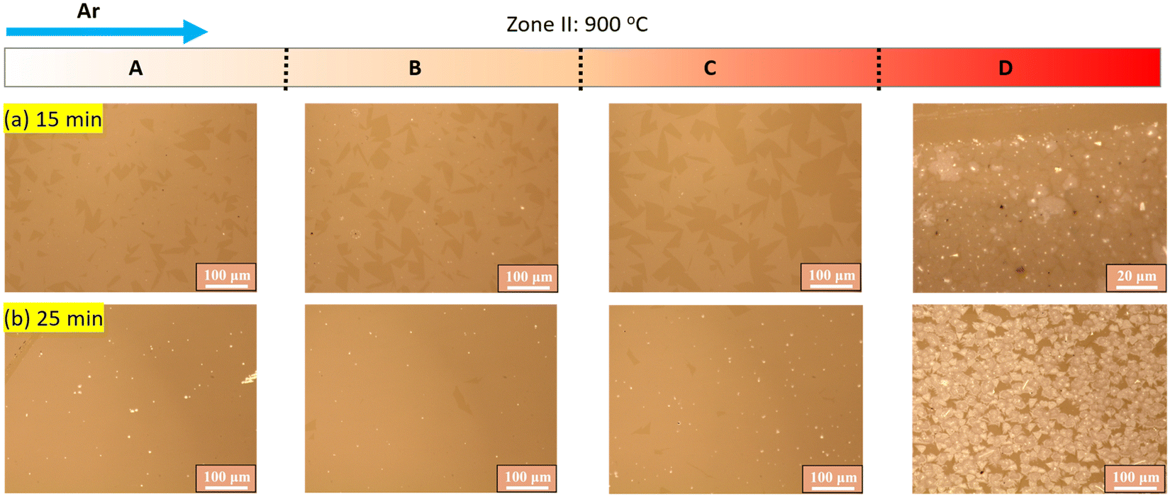 | ||
| Fig. 3 Optical microscope images of zone II taken as a function of growth time. The temperature in zone II is set to be 900 °C. | ||
Next, we investigate the impact of introducing S vapor after the evaporation of the W precursor. At a deposition temperature of 800 °C, most of the WS2 crystals are deposited in subzone A, as shown in Fig. 4a. Increasing the temperature to 850 °C would result in the observation of monolayer WS2 flakes collected in subzone A, accompanied by a decrease in the quantity of the monolayer WS2 in subzone B (Fig. 4b). In subzones C and D, thick flower-like WS2 materials are witnessed. When the temperature of zone II is raised to 900 °C, the continuous monolayer WS2 film can be obtained in subzones A, B, and C, but thick dispersed WS2 domains are still present in subzone D (Fig. 4c).
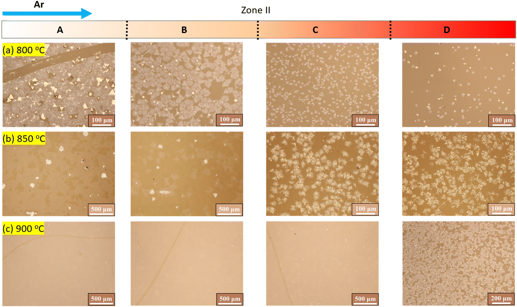 | ||
| Fig. 4 Optical microscope images of the products obtained in zone II when S was heated after the evaporation of the W source. The temperatures of zone II are (a) 800 °C, (b) 850 °C, and (c) 900 °C. | ||
At a temperature of 930 °C in zone I, NaxWOy vaporizes and is transported to zone II by the carrier gas. Without introducing the S vapor, liquid droplets of NaxWOy may form on the substrates in zone II. The deposition rate of these liquid droplets is linearly carried with s, where s = P/Peq. Here, P is the actual partial pressure of NaxWOy, and Peq is the saturation pressure above liquid NaxWOy. At a lower temperature of 800 °C, a large temperature gradient is formed in subzone A, resulting in the formation of numerous NaxWOy droplets on the substrate. When S vapor is introduced, the liquid droplets would react with S to form WS2 crystals. These crystals aggregate later to form a thick WS2 film. Since most of the NaxWOy species are deposited in subzone A, the amount of NaxWOy vapor transported downstream to subzones B, C, and D is significantly reduced, leading to a decrease in the product in those regions. When the temperature in zone II is increased to 850 °C, the density of NaxWOy droplets is reduced due to a decrease in the temperature gradient in subzone A. The reaction of the NaxWOy droplets with S vapor results in the formation of thick WS2 crystals on the substrate, which act as nuclei for the monolayer WS2 growth. The temperature gradient in subzone A is greater than in subzone B, resulting in a faster WS2 growth rate in subzone A and larger monolayer WS2 triangles. As the temperature gradient gradually increases, the density of droplets in subzone C and subzone D increases, forming a flower-like product. When the temperature in zone II reaches 900 °C, a uniform monolayer WS2 film forms in subzones A, B, and C, indicating the uniform deposition of WS2 on the substrates. However, the large temperature gradient in subzone D would lead to thick WS2 deposition. The above results and discussion indicate that achieving a uniform temperature distribution in the deposition zone is crucial for forming a uniform monolayer WS2 film. Additionally, it is important to precisely control the growth time to prevent overgrowth.
Notably, introducing S at an appropriate time can lead to the formation of nanowires/nanobelts on substrates when the temperature of zone II is 850 °C, as shown in Fig. S1 (ESI†). Subzone A exhibits a thick WS2 film due to a significant temperature gradient, while nanowires and nanobelts are observed in subzones B, C, and D. The formation of one-dimensional (1D) nanostructures via the vapor–liquid–solid (VLS) mechanism can be readily explained due to the formation of NaxWOy droplets on the substrate. In zone II, NaxWOy species are deposited onto the substrate as tiny droplets, reacting with the S vapor to form WS2 that dissolves in the droplets. Upon reaching supersaturation, WS2 is deposited onto the substrate through continuous deposition from the droplets, ultimately creating 1D WS2 nanostructures. Previous studies have reported the growth of MoS2 nanobelts on the NaCl substrate, with the formation of one-dimensional (1D) MoS2 nanostructures attributed to the VLS mechanism.39 Here, the construction of NaxWOy liquid droplets is critical to the growth of 1D WS2, and thus, S should be introduced after the formation of NaxWOy liquid droplets and not too late. Otherwise, tiny droplets will aggregate into larger ones that are too heavy for the deposited WS2 to push away, forming only large crystals. Small NaxWOy liquid droplets can be formed accidentally in other synthesis conditions, resulting in the frequent observation of 1D-like WS2 nanostructures in zone II (Fig. S2, ESI†).
Based on the obtained results, we propose mechanisms for the Na2WO4-assisted growth of WS2, as illustrated in Fig. 5. When S is introduced before the evaporation of NaxWOy (Fig. 5a), most of the vapor species transported downstream are WS2. At high deposition temperatures, the deposition of WS2 is slow, resulting in the growth of monolayer WS2 triangles and, thus, a monolayer film. However, if the growth time is too long, overgrowth may occur on the defects or grain boundaries of the as-formed monolayer, leading to films with thick domains. At low deposition temperatures, the deposition of WS2 is fast, leading to the growth of thick WS2 triangles and, thus, a non-uniform thick WS2 film. When S is introduced after the evaporation of NaxWOy (Fig. 5b), the vapor species transported downstream in the early stage is NaxWOy. The NaxWOy liquid droplets can form on the substrate, and when S is introduced, NaxWOy would react with S to form WS2 species that can dissolve in the droplets. After supersaturation, WS2 will deposit from the droplets. If the droplets are large enough, WS2 will gradually deposit from them, forming large crystals. If the droplets are of adequate size, a VLS mechanism can occur, forming 1D WS2. If the droplets are too small, they will transform into WS2 nanocrystals immediately upon reacting with S, which will act as the nuclei of monolayer WS2, forming a monolayer WS2 film. In fact, most monolayer WS2 triangle flakes exhibit a thick dot at their center (Fig. S3, ESI†). It is worth noting that the thick dots were consistently observed at the center of monolayer WS2 triangles, regardless of the sequence and duration of the S introduction. This observation suggests the crucial role of the thick dot in the growth of monolayer WS2. In addition, the monolayer WS2 film can be scaled up if a horizontal tube furnace with a larger diameter and longer heating zone is used, according to the growth mechanism.
 | ||
| Fig. 5 Growth mechanism. (a) S is introduced before the evaporation of NaxWOy. (b) S is introduced after the evaporation of NaxWOy. | ||
To assess the quality of the monolayer film deposited at 900 °C, Raman and PL spectroscopy were employed. The film synthesized with S introduction before the evaporation of the W source is labeled as sample #1, and the film synthesized with S introduction after the evaporation of the W source is labeled as sample #2. Both films exhibited similar Raman spectra (Fig. 6a), consistent with the monolayer WS2.40,41 However, their PL spectra are different, as shown in Fig. 6b. The PL spectrum of sample #1 is stronger than that of sample #2, and the peak shapes are different. Deconvolution of the peaks (Fig. 6c and d) reveals three peaks corresponding to exciton (X0: ∼2.01 eV), trion (XT: ∼1.98 eV), and defect-related emission (XD: ∼1.93 eV).42 The intensity ratios between X0 and XD are 1.38 and 0.42 for samples #1 and #2, respectively, indicating that the contribution from XT is larger for sample #2. The formation of XT is strongly related to the free electron concentration in WS2, with higher concentrations contributing more to the PL emission.43 Therefore, sample #2 has a higher free electron concentration. Though higher electron concentration is beneficial for the formation of trions, the overall possibility of the formation of both excitons and trions reduces, leading to the weak PL intensity for sample #2.44 Intrinsic n-doping for WS2 is commonly attributed to S vacancies,45 inferring that the higher free electron concentration in sample #2 suggests a higher defect concentration overall. Due to the introduction of S vapor before the evaporation of NaxWOy for sample #1, a reduced number of S vacancies is anticipated compared to sample #2, which is consistent with the observed PL results. These results suggest the high crystal quality of sample #1 in comparison with sample #2.
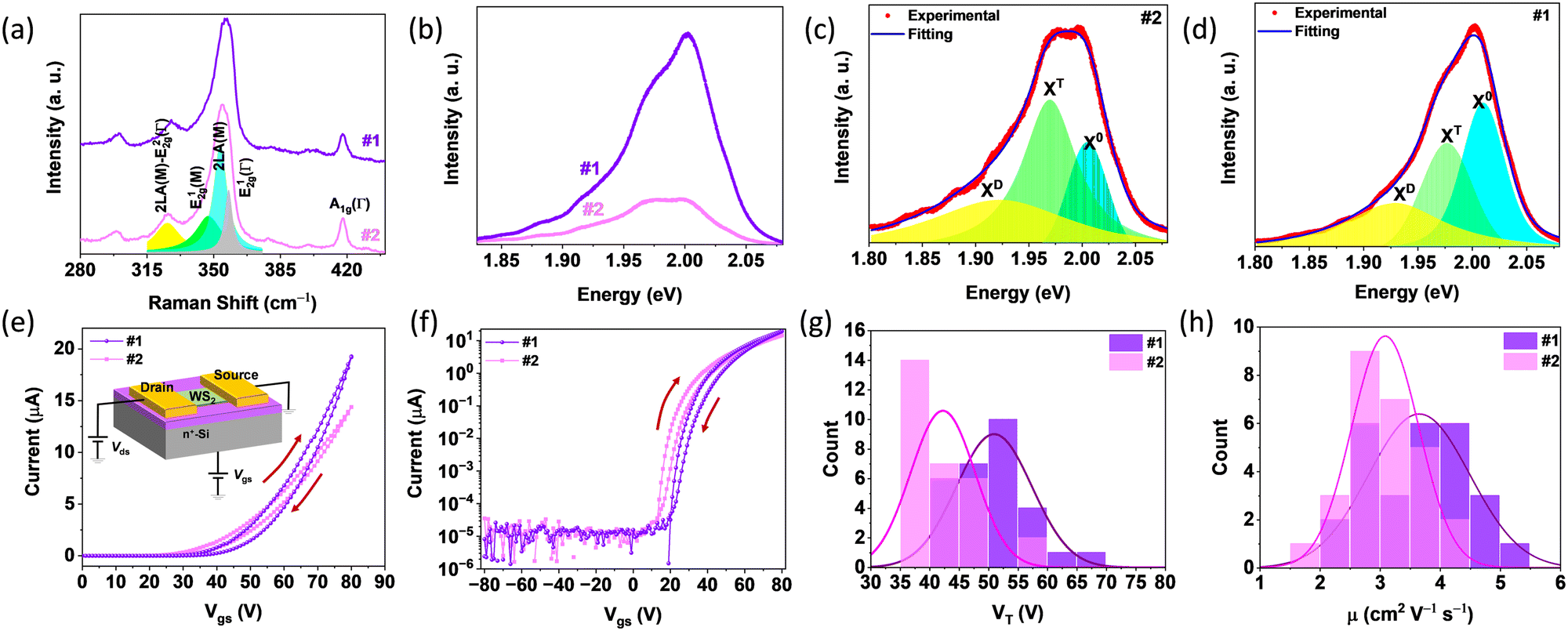 | ||
| Fig. 6 Raman, PL spectra and electrical properties of WS2. (a) Raman spectra. (b) PL spectra. (c) PL spectrum of sample #1. (d) PL spectrum of sample #2. (e) Typical transfer curves. Inset: Schematic of the device structure. (f) Log-plot of the transfer curves. (g) Statistical diagram of the threshold voltage. (h) Statistical diagram of the electron mobility. The arrows in (e) and (f) indicate the sweeping directions during the measurements. | ||
Back-gated field effect transistors (FETs) were fabricated to evaluate the electrical properties of the films. The structure of the devices is shown in the inset of Fig. 6e, SiO2 with a thickness of 285 nm was used as the dielectric and n+-doped Si was used as the backgate electrode. Fig. 6e shows the typical transfer curves of FETs based on samples #1 and #2, indicating that both exhibit n-type conductivity as the drain–source current increases with the gate voltage. Both curves exhibit hysteresis due to the charge traps in the WS2 channel, and/or in the interface between WS2 and SiO2.46 Log plots of the transfer curves are presented in Fig. 6f to provide a better understanding of the FETs. Both FETs' current on/off ratio exceeds 106, indicating a good device performance. Based on sample #1, the FETs display a larger threshold voltage than those based on sample #2, suggesting the higher n-doping in sample #2, consistent with the PL results. To further confirm this hypothesis, threshold voltages were extracted from tens of FETs, and the statistical diagrams are presented in Fig. 6g, which demonstrate that FETs based on sample #2 have a smaller threshold voltage. This result again indicates that sample #1 has a lower electron concentration than sample #2. The electron mobilities were extracted from the transfer curves, and the statistical diagrams are presented in Fig. 6h. FETs based on sample film #1 exhibit a higher average mobility, indicating better quality than sample #2, consistent with the observed PL results. Notably, both the threshold voltages and mobilities were extracted from the forward sweeping for simplicity. Due to the small hysteresis, the difference for forward and backward sweeping is small.
3. Conclusion
In summary, we have presented a detailed investigation into the Na2WO4-assisted synthesis of WS2. Our findings reveal that the substrate temperature and the sequence and duration of S vapor introduction are critical factors in tuning the morphology of the WS2 products. A large-area, continuous monolayer film could be obtained with a suitable substrate temperature and growth time. A lower substrate temperature could lead to the formation of thick films, and wire-like nanostructures. Furthermore, the optical and electrical properties of the monolayer WS2 film are closely related to the introduction sequence of S vapor. The film with the introduction of S before the evaporation of the W source showed a higher PL emission intensity, and FETs based on the film exhibited larger threshold voltages and higher electron mobilities. These findings suggest that the Na2WO4-assisted method for the growth of WS2 is highly controllable and reproducible, and the obtained monolayer WS2 films have a high quality, suitable for electronic applications.4. Experimental section
Material synthesis
In the synthesis, a two heating zone horizontal furnace with a quartz tube was used. The mixture powder of WO3 (99.9%) and Na2WO4 (99.9%) with a mass ratio of 1:2 was used as the W source. The mixture powder (0.1 g) was placed in a quartz boat, which was inserted in a quartz tube and placed in the center of zone I. Several pieces of sapphire substrates were placed in zone II. S powder (200 g) was placed in a corundum boat, which was placed on the upstream side of the quartz tube outside the heating zone of the furnace. S powder was heated by a heating belt. Before heating, the pressure inside the quartz tube was pumped to 1 Pa by a mechanical pump. Then Ar gas flow (200 sccm) was introduced into the quartz tube as a carrier gas. Typically, zone I and zone II were heated simultaneously. Zone I was heated to 930 °C for 30 min and held for 40 min; zone II was heated to 900 °C for 30 min and held for 40 min. S was heated to 150 °C for 6 min and held for 80 min. The pressure inside the quartz tube was maintained at ∼120 Pa during the reaction. After the reaction, the furnace cooled down naturally.
Material characterizations
The morphology of the products was characterized by an optical microscope (Olympus, BX70). A Raman spectrometer (SR-5001-A-R, Andor) with a 532 nm laser was used to obtain Raman and PL spectra of the products.Device fabrication
The as-synthesized products were transferred onto SiO2 (285 nm)/Si substrate by the polystyrene-assisted transfer method.47 Then, standard photolithography was used to define the channel areas. Ion-etching was used to etch the product outside the channel area. Standard photolithography was used again to define the drain and source electrode areas. Bi/Au (30/60 nm) were deposited as electrodes by vacuum thermal evaporation.Device measurements
The performance of field effect transistors was measured in a vacuum probe station (PicoFemto). A semiconductor analyzer (B1500A, Keysight) was used to measure the output and transfer curves of the transistors. The pressure was maintained at ∼3 × 10⁻⁴ Pa during the measurements. Constant current density (10−2 μA μm−1) was used to extract the threshold voltage.Conflicts of interest
There are no conflicts of interest to declare.Acknowledgements
This work was supported by the National Natural Science Foundation of China (Grant No. 61975024 and 62074024), the Sichuan Science and Technology Program (Grant No. 2023YFH0090 and 2023NSFSC0365), the Natural Science Foundation of Sichuan Province (Grant No. 2022NSFSC0042), and the National Key Research and Development Program of China (Grant No. 2019YFB2203504).References
- Y. Meng, X. Li, X. Kang, W. Li, W. Wang, Z. Lai, W. Wang, Q. Quan, X. Bu, S. Yip, P. XIe, D. Chen, D. Li, F. Wang, C.-F. Yeung, C. Lan, C. Liu, L. Shen, Y. Lu, F. Chen, C.-Y. Wong and J. C. Ho, Nat. Commun., 2023, 14, 2431 CrossRef CAS PubMed.
- Y. Meng, F. Li, C. Lan, X. Bu, X. Kang, R. Wei, S. Yip, D. Li, F. Wang, T. Takahashi, T. Hosomi, K. Nagashima, T. Yanagida and J. C. Ho, Sci. Adv., 2020, 6, eabc6389 CrossRef CAS.
- D. Li, C. Lan, A. Manikandan, S. Yip, Z. Zhou, X. Liang, L. Shu, Y.-L. Chueh, N. Han and J. C. Ho, Nat. Commun., 2019, 10, 1664 CrossRef PubMed.
- Y. Guo, D. Liu, C. Miao, J. Sun, Z. Pang, P. Wang, M. Xu, N. Han and Z. Yang, Nanotechnology, 2021, 32, 145203 CrossRef CAS PubMed.
- D. Liu, F. Liu, J. Zhang, Z. Sa, M. Wang, S. Yip, J. Wan, P. Li and Z. Yang, J. Electron. Sci. Technol., 2023, 21, 100196 CrossRef.
- D. Liu, Y. Yin, F. Liu, C. Miao, X. Zhuang, Z. Pang, M. Xu, M. Chen and Z. Yang, Rare Met., 2022, 41, 1753–1760 CrossRef CAS.
- Z. Sa, F. Liu, D. Liu, M. Wang, J. Zhang, Y. Yin, Z. Pang, X. Zhuang, P. Wang and Z. Yang, J. Semicond., 2022, 43, 112302 CrossRef.
- G. Fiori, F. Bonaccorso, G. Iannaccone, T. Palacios, D. Neumaier, A. Seabaugh, S. K. Banerjee and L. Colombo, Nat. Nanotechnol., 2014, 9, 768–779 CrossRef CAS PubMed.
- K. F. Mak and J. Shan, Nat. Photonics, 2016, 10, 216–226 CrossRef CAS.
- H. Li, X. Wang, X. Zhu, X. Duan and A. Pan, Chem. Soc. Rev., 2018, 47, 7504–7521 RSC.
- Y. Liu, X. Duan, H.-J. Shin, S. Park, Y. Huang and X. Duan, Nature, 2021, 591, 43–53 CrossRef CAS PubMed.
- A. Elbanna, H. Jiang, Q. Fu, J.-F. Zhu, Y. Liu, M. Zhao, D. Liu, S. Lai, X. W. Chua, J. Pan, Z. Shen, L. Wu, Z. Liu, C.-W. Qiu and J. Teng, ACS Nano, 2023, 17, 4134–4179 CrossRef CAS PubMed.
- C. Lan, Z. Shi, R. Cao, C. Li and H. Zhang, Nanoscale, 2020, 12, 11784–11807 RSC.
- J. Zhang, F. Liu, D. Liu, Y. Yin, M. Wang, Z. Sa, L. Sun, X. Zheng, X. Zhuang, Z. Lv, W. Mu, Z. Jia, Y. Tan, F. Chen and Z. Yang, Mater. Today Phys., 2023, 31, 100997 CrossRef CAS.
- C. Lan, C. Li, J. C. Ho and Y. Liu, Adv. Electron. Mater., 2021, 7, 2000688 CrossRef CAS.
- S. Manzeli, D. Ovchinnikov, D. Pasquier, O. V. Yazyev and A. Kis, Nat. Rev. Mater., 2017, 2, 17033 CrossRef CAS.
- Z. Wei, B. Li, C. Xia, Y. Cui, J. He, J. B. Xia and J. Li, Small Methods, 2018, 2, 1800094 CrossRef.
- W. Zhu, T. Low, H. Wang, P. Ye and X. Duan, 2D Mater., 2019, 6, 032004 CrossRef CAS.
- Y. Wei, C. Lan, S. Zhou and C. Li, Appl. Sci., 2023, 13, 11037 CrossRef CAS.
- X. Jia, C. Lan and C. Li, Infrared Laser Eng, 2022, 51, 20220065 CrossRef.
- C. Ding, H. Jia, Q. Sun, Z. Yao, H. Yang, W. Liu, X. Pang, S. Li, C. Liu, T. Minari, J. Chen, X. Liu and Y. Song, J. Mater. Chem. C, 2021, 9, 7829–7851 RSC.
- Y. Shi, H. Li and L.-J. Li, Chem. Soc. Rev., 2015, 44, 2744–2756 RSC.
- X. Xu, T. Guo, H. Kim, M. K. Hota, R. S. Alsaadi, M. Lanza, X. Zhang and H. N. Alshareef, Adv. Mater., 2022, 34, 2108258 CrossRef CAS PubMed.
- T. Kang, T. W. Tang, B. Pan, H. Liu, K. Zhang and Z. Luo, ACS Mater. Au, 2022, 2, 665–685 CrossRef CAS PubMed.
- L. Tang, J. Tan, H. Nong, B. Liu and H.-M. Cheng, Acc. Mater. Res., 2020, 2, 36–47 CrossRef.
- Y. Zhang, Y. Yao, M. G. Sendeku, L. Yin, X. Zhan, F. Wang, Z. Wang and J. He, Adv. Mater., 2019, 31, 1901694 CrossRef CAS PubMed.
- C. Lan, C. Li, Y. Yin and Y. Liu, Nanoscale, 2015, 7, 5974–5980 RSC.
- T. Li, W. Guo, L. Ma, W. Li, Z. Yu, Z. Han, S. Gao, L. Liu, D. Fan, Z. Wang, Y. Yang, W. Lin, Z. Luo, X. Chen, N. Dai, X. Tu, D. Pan, Y. Yao, P. Wang, Y. Nie, J. Wang, Y. Shi and X. Wang, Nat. Nanotechnol., 2021, 16, 1201–1207 CrossRef CAS PubMed.
- L. Liu, T. Li, L. Ma, W. Li, S. Gao, W. Sun, R. Dong, X. Zou, D. Fan, L. Shao, C. Gu, N. Dai, Z. Yu, X. Chen, X. Tu, Y. Nie, P. Wang, J. Wang, Y. Shi and X. Wang, Nature, 2022, 605, 69–75 CrossRef CAS.
- J. Li, S. Wang, L. Li, Z. Wei, Q. Wang, H. Sun, J. Tian, Y. Guo, J. Liu and H. Yu, Small Sci., 2022, 2, 2200062 CrossRef CAS.
- C. Lan, Z. Zhou, Z. Zhou, C. Li, L. Shu, L. Shen, D. Li, R. Dong, S. Yip and J. C. Ho, Nano Res., 2018, 11, 3371–3384 CrossRef CAS.
- J. Wang, X. Xu, T. Cheng, L. Gu, R. Qiao, Z. Liang, D. Ding, H. Hong, P. Zheng, Z. Zhang, Z. Zhang, S. Zhang, G. Cui, C. Chang, C. Huang, J. Qi, J. Liang, C. Liu, Y. Zuo, G. Xue, X. Fang, J. Tian, M. Wu, Y. Guo, Z. Yao, Q. Jiao, L. Liu, P. Gao, Q. Li, R. Yang, G. Zhang, Z. Tang, D. Yu, E. Wang, J. Lu, Y. Zhao, S. Wu, F. Ding and K. Liu, Nat. Nanotechnol., 2022, 17, 33–38 CrossRef CAS.
- S. Li, S. Wang, D.-M. Tang, W. Zhao, H. Xu, L. Chu, Y. Bando, D. Golberg and G. Eda, Appl. Mater. Today, 2015, 1, 60–66 CrossRef.
- J. Zhou, J. Lin, X. Huang, Y. Zhou, Y. Chen, J. Xia, H. Wang, Y. Xie, H. Yu and J. Lei, Nature, 2018, 556, 355–359 CrossRef CAS PubMed.
- W. Han, K. Liu, S. Yang, F. Wang, J. Su, B. Jin, H. Li and T. Zhai, Sci. China: Chem., 2019, 62, 1300–1311 CrossRef CAS.
- C. Lan, R. Zhang, H. Wu, S. Wen, R. Zou, X. Kang, C. Li, J. C. Ho, Y. Yin and Y. Liu, Appl. Mater. Today, 2021, 25, 101234 CrossRef.
- J. D. Harris and A. W. Rusch, J. Chem. Educ., 2013, 90, 235–238 CrossRef CAS.
- I. V. Markov, Crystal Growth for Beginners: Fundamentals of Nucleation, Crystal Growth and Epitaxy, World Scientific Publishing Co. Pte. Ltd., Hong Kong, 2nd edn, 2003 Search PubMed.
- S. Li, Y.-C. Lin, W. Zhao, J. Wu, Z. Wang, Z. Hu, Y. Shen, D.-M. Tang, J. Wang, Q. Zhang, H. Zhu, L. Chu, W. Zhao, C. Liu, Z. Sun, T. Taniguchi, M. Osada, W. Chen, Q.-H. Xu, A. T. Shen Wee, K. Suenaga, F. Ding and G. Eda, Nat. Mater., 2018, 17, 535–542 CrossRef CAS PubMed.
- P. K. Nayak, C.-H. Yeh, Y.-C. Chen and P.-W. Chiu, ACS Appl. Mater. Interfaces, 2014, 6, 16020–16026 CrossRef CAS PubMed.
- C. Lan, X. Kang, R. Wei, Y. Meng, S. Yip, H. Zhang and J. C. Ho, ACS Appl. Mater. Interfaces, 2019, 11, 35238–35246 CrossRef CAS PubMed.
- P. K. Chow, R. B. Jacobs-Gedrim, J. Gao, T.-M. Lu, B. Yu, H. Terrones and N. Koratkar, ACS Nano, 2015, 9, 1520–1527 CrossRef CAS PubMed.
- N. Peimyoo, W. Yang, J. Shang, X. Shen, Y. Wang and T. Yu, ACS Nano, 2014, 8, 11320–11329 CrossRef CAS PubMed.
- S. Tongay, J. Zhou, C. Ataca, J. Liu, J. S. Kang, T. S. Matthews, L. You, J. Li, J. C. Grossman and J. Wu, Nano Lett., 2013, 13, 2831–2836 CrossRef CAS PubMed.
- S.-S. Chee, C. Oh, M. Son, G.-C. Son, H. Jang, T. J. Yoo, S. Lee, W. Lee, J. Y. Hwang and H. Choi, Nanoscale, 2017, 9, 9333–9339 RSC.
- C. Lan, X. Kang, Y. Meng, R. Wei, X. Bu, S. Yip and J. C. Ho, Nano Res., 2020, 13, 3278–3285 CrossRef CAS.
- A. Gurarslan, Y. Yu, L. Su, Y. Yu, F. Suarez, S. Yao, Y. Zhu, M. Ozturk, Y. Zhang and L. Cao, ACS Nano, 2014, 8, 11522–11528 CrossRef CAS PubMed.
Footnote |
| † Electronic supplementary information (ESI) available. See DOI: https://doi.org/10.1039/d3ma00867c |
| This journal is © The Royal Society of Chemistry 2023 |