DOI:
10.1039/D3MA00775H
(Paper)
Mater. Adv., 2023,
4, 6381-6388
Enhancement of upconversion photoluminescence in phosphor nanoparticle thin films using metallic nanoantennas fabricated by colloidal lithography†
Received
28th September 2023
, Accepted 31st October 2023
First published on 2nd November 2023
Abstract
Lanthanide-doped upconversion nanoparticles (UCNPs), as multifunctional light sources, are finding utility in diverse applications ranging from biotechnology to light harvesting. However, the main challenge in realizing their full potential lies in achieving bright and efficient photon upconversion (UC). In this study, we present a novel approach to fabricate an array of gold nanoantennas arranged in a hexagonal lattice using a simple and inexpensive colloidal lithography technique, and demonstrate a significant enhancement of UC photoluminescence (UCPL) by up to 35-fold through plasmon-enhanced photoexcitation and emission. To elucidate the underlying physical mechanisms responsible for the observed UCPL enhancement, we provide a comprehensive theoretical and experimental characterization, including a detailed photophysical description and numerical simulations of the spatial electric field distribution. Our results shed light on the fundamental principles governing the enhanced UCNPs and pave the way for their potential applications in photonic devices.
Introduction
Lanthanide-doped upconversion nanoparticles (UCNPs) have attracted much attention due to their nonlinear character, which enables the conversion of low-energy photons into higher-energy ones via energy transfer between the long-lived and ladder-like energy levels of lanthanide ions.1–3 This intriguing phenomenon endows these nanomaterials with tremendous potential for applications in various fields, including biotechnology,4–8 thermometry,9,10 light harvesting,11,12 or anti-counterfeiting.13–15 However, the low efficiency of nonlinear processes and the small absorption cross section of dopants limit the brightness of UCNPs and pose a challenge to the development of the UC-based technology.16–18 In recent years, several strategies have been developed to overcome this limitation. The most successful ones can be divided into those that optimize intrinsic material properties, such as composition and crystalline structure, including surface modification,19–21 doping level,3,22 or core/shell architecture,22,23 and those that tune the optical environment of the UC materials.24 Among the latter, localized surface plasmon resonances (LSPRs) have been demonstrated to be an excellent choice for modulating the emission of UC materials.25–29 LSPRs arise from the collective oscillations of free electrons on the metal surface under illumination, resulting in a significant enhancement of the electric field intensity in the vicinity of the resonant NPs.30 Such an enhanced electric field can drastically alter the photoexcitation or the emission dynamics if the LSPR modes match the excitation or emission bands of nearby emitters.26 Indeed, Ag nanocavities or gold NPs supporting an LSPR mode overlapping with the emission of UCNPs have enabled an enhancement of the radiative decay rate, thereby improving the UCPL intensity.31,32 It has also been shown that metallic nanostructures resonant with the excitation bands of UCNPs give rise to increased UCPL due to absorption enhancement.33–35 In all approaches, controlling the spectral position of the LSPRs is the key point to demonstrate UCPL enhancement. This can be achieved by tuning the material properties and the dimensions of the individual plasmon nanoparticles.36–38 For example, core36,37 and core/shell38–40 metallic nanorods have been carefully synthesized to support LSPRs tuned to the excitation or emission of UCNPs, resulting in several-fold enhancement of UCPL. An alternative route to tailoring LSPRs relies on the use of lithographic methods. Indeed, a variety of techniques have been used for this purpose, including laser interference,34 nanoimprint,33,41 electron beam42–45 or a combination of lithography, chemical etching,35,46 and thermal evaporation.33,34 Although, these techniques allow the fabrication of nanostructures with fine precision, they have the disadvantage of requiring costly steps.
Herein, we present a facile method to fabricate an array of regular gold nanoantennas arranged in a hexagonal lattice to enhance the UC emission of NaYF4:Yb3+,Er3+ (abbreviated as NaYF) NPs. The method involves the use of a monolayer of self-assembled polystyrene (PS) spheres, as an evaporation mask for metal deposition and the subsequent removal of the PS layer by a mechanical process. Note that similar masked deposition has previously been used to prepare irregular and random metal nanoparticle arrays.29 Our approach combines the advantages of self-assembly and thermal evaporation as simple, inexpensive, reproducible and large scale, and allows its combination with thin layers of NaYF NPs, the workhorse material for UC. By controlling the dimensions of the mask, the LSPRs of the gold nanostructures are tuned to match both the excitation and emission bands of the UCNPs. As a result, we demonstrate a large UCPL enhancement, up to 20 and 35 times for green and red emission bands of Er3+ cations, respectively. The underlying mechanism is revealed by a detailed photophysical characterization together with numerical simulations. Our analysis confirms that the presence of resonant gold NPs significantly enhances the NaYF absorption and tunes the UC emission. Plasmon-mediated excitation accelerates the filling of the Er3+ energy levels and increases the radiative decay rate of Er3+ transitions. Despite its simplicity, our approach provides an effective way to improve the brightness of UC thin films and highlights the potential of colloidal lithography to develop bright, large-area UC coatings that will be of interest for applications in imaging, sensing, or security.
Results and discussion
Metallic nanoparticle array coated with UCNPs
First an array of gold nanostructures is fabricated by colloidal lithography, which involves three main steps as described in the Methods section and illustrated in Fig. 1a. Briefly, a colloidal mask consisting of an ordered monolayer of submicron PS spheres is prepared using a wedge evaporation technique. Convective methods have proven useful in directing the assembly of nanoparticles from dilute suspensions as the dispersant is removed. In the particular case of monodisperse beads, the evaporation of the dispersant forces the nanoparticles to arrange in the meniscus formed between substrate, dispersion and air. In fact, careful design of the meniscus curvature during drying using a wedge-shaped cell allows the assembly of polymer beads into cm2-sized ordered monolayers. By controlling the humidity, temperature and concentration of the suspension, an optimal evaporation and deposition rate of the spheres is achieved, resulting in a monolayer of PS spheres arranged in a hexagonal lattice – see Fig. 1a-I. A 100 nm layer of gold is then deposited over such a monolayer by thermal evaporation. Removal of the PS spheres by a mechanical process results in a periodic array of gold nanostructures arranged in a honeycomb lattice, with nanoparticles located at the vertices of each hexagon in the lattice, as shown in Fig. 1a-II. Fig. 1b displays an atomic force microscope (AFM) image of the array of gold nanostructures, which allows the size and shape of the gold nanoparticles and their periodic distribution to be accurately estimated. In fact, the average height of the gold nanostructures corresponds to ∼100 nm, which is consistent with the thickness of the evaporated gold layer. Notice that a similar method can be used to fabricate large-scale arrays of silver nanoparticles. Finally, a UC phosphor thin film is deposited over the metal array by spin-coating a suspension containing NaYF NPs and poly(acrylic acid) (PAA) – see Fig. 1a-III. NaYF NPs were synthesized in an inert atmosphere, see the Methods section and the ESI† (Fig. S1) for details. They are uniform and show a rod-like morphology with an average size of (50 ± 2) nm × (35 ± 2) nm. The addition of PAA increases the viscosity of the dispersion and facilitates the processing of homogeneous coatings. Fig. 1c shows scanning electron microscope (SEM) images of the gold array before and after deposition of a UCNP film with a thickness of ∼100 nm. In particular, the left side of Fig. 1c shows a top view of the array, while the right side displays a top view of the same array coated with a NaYF-PAA film (referred to as Au/UC). The NaYF NPs exhibit uniform coverage of the space between the metal nanoparticles (see also Fig. S2, ESI†). It is noteworthy that unlike the UCNP film, the gold nanoparticle array does not completely cover the glass substrate. Thus, the area of the UC film without gold nanoparticles serves as a reference (referred to as UC) in the photophysical characterization that we show next.
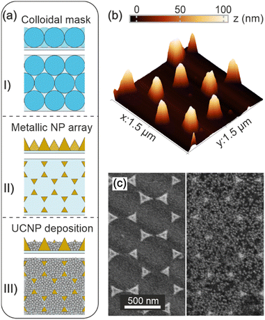 |
| | Fig. 1 (a) Schematic description of the fabrication process of the gold nanoparticle array coated with UCNPs. It includes (I) the preparation of a colloidal mask made of a polystyrene sphere monolayer, (II) 100 nm metal evaporation and mask removal, and (III) the deposition of a UC coating. (b) Atomic force microscope (AFM) image of the gold nanoparticle array. (c) Backscattered electron (BSE) scanning electron microscope (SEM) images of the top view of gold nanoparticles without (left side) and with (right side) the UC coating. | |
Spectroscopic characterization
We measure the ballistic transmittance of the samples, see Fig. 2a. The UC coating (black long dashed line) on glass is fairly transparent, with ballistic transmittance values above ∼85% in a wide spectral range between 400 and 1200 nm. The metal nanostructure array shows a reduced transmittance (∼75%) (black short dashed line) with a pronounced dip between ∼700 and ∼1200 nm. The lowest transmittance value (∼60%) is observed at ∼950 nm, close to the excitation wavelength used to pump the UCNPs (980 nm, marked as a grey dashed line). In addition, the transmittance also features a shallower dip between ∼500 and ∼700 nm, overlapping with the green and red emission bands of Er3+ -see grey bands in Fig. 1a. The black solid line in Fig. 2a represents the transmittance of the UCNP layer deposited over the metal array. The presence of a thin film alters the refractive index environment of the metal nanostructures, causing a slight shift in the features observed in the transmittance spectrum. In addition, it can be seen that the modes that are supported by the antennas determine the response of the UC film when it is deposited on them.
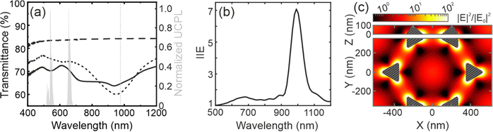 |
| | Fig. 2 (a) Experimental transmittance of a UC coating over glass (black long dashed line), a gold nanoantenna array (black short dashed line) and a UC coating over a gold nanoantenna array (black solid line. The emission bands of NaYF UCNPs are included as grey bands. The excitation wavelength (980 nm) is also shown as a grey dashed line. (b) Calculated integrated intensity enhancement (IIE) for the UC coating over a gold nanoantenna array. (c) Simulated electric field intensity for the same system at 980 nm. Two sections are shown: the top panel displays a XY plane (z = 0 nm), while the bottom panel shows an XZ plane intersecting two of the nanoantennas. | |
Numerical simulations
To investigate the physical origin of the resonances, we perform finite difference time domain (FDTD) simulations under plane wave illumination. The calculated reflectance of the metal array is presented in Fig. S3 (ESI†). We calculate the integrated intensity enhancement (IIE) for a given wavelength (λ), as the ratio between the electric field intensity in the volume occupied by the UCNPs in the presence and in the absence of the gold array, using the following equation:| |  | (1) |
where r is a position in space, |EAu/UC|2 and |Eref|2 are the electric field intensities in the Au/UC film and the UC reference, respectively, while |E0,Au/UC|2 and |E0,ref|2 are the incident electric field intensities of the illumination source in each case, respectively. Fig. 2b presents the IIE as a function of the excitation wavelength (λex). A pronounced peak is observed at ∼950 nm, which we attribute to the excitation of an LSPR in the gold nanoparticles.33,34 Nevertheless, the full width at half maximum at resonance for the calculation is smaller than that observed in the transmittance measurements. We ascribe this discrepancy to inhomogeneities in the size and shape of the fabricated gold nanostructures. Fig. 2c displays the spatial distribution of the electric field intensity simulated at λex = 980 nm. A strong electric field intensity is observed around the edges of the gold nanoparticles, with the field mostly concentrated at their vertices, as expected for an LSPR. The metal nanoparticles in the array allow the efficient exchange of near-field and far-field energy at the nanoscale, acting as individual optical antennas, or simply nanoantennas. Although the calculations show hot spots of more than 100-fold field intensity, the integral over the thin film volume gives a 7-fold IIE at ∼980 nm, which overlaps with the λex of the UCNPs. Similar behavior is observed for the electric field intensity calculated at the emission wavelengths (λem) of the UCNPs, but with lower IIE values (less than 2-fold). In particular, calculations show moderate IIE in the visible with ∼1.5-fold in the red (∼700 nm) and ∼1.2-fold in the green (∼540 nm) – see Fig. S4 (ESI†). Thus, our simulations indicate that the main contribution to the overall UCPL enhancement associated with our nanoantennas is expected to come from a resonant excitation.
UCPL enhancement assessment
To study the effect of the LSPR supported by the nanoantennas on the emission properties of UCNPs, we use a 980 nm laser, which coincides with the 2F7/2 to 2F5/2 transition of Yb3+ ions.31,47 Upon excitation, 980 nm light is absorbed by Yb3+ and energy is transferred to Er3+, resulting in green and red emission see Fig. 3a. These emission bands are centered at ∼541 and ∼655 nm, respectively, and are associated with the 4S3/2, 2H11/2, and 4F9/2 transitions to the 4I15/2 ground state of Er3+ see Fig. S5 (ESI†).48,49 In the presence of nanoantennas, the UCPL intensity is significantly improved compared to that of a reference film, up to ∼10- and ∼20-fold for green and red emission, respectively. Metal nanoparticle-supported LSPRs can couple with the excitation and the emission of the UCNPs as discussed above, resulting in LSPR-mediated UCPL enhancement at both λex and λem.25,34,50 In the low excitation power regime, the UCPL is proportional to the square of the fraction of light absorbed by the UCNPs at λex.33,51 Also, in view of the simulations, according to the reciprocity theorem,52 a further, albeit small, enhancement of the UCPL is expected at λem. As a result, the UCPL enhancement is mainly due to plasmon-mediated resonant photoexcitation and is greater for the red band than for the green band.
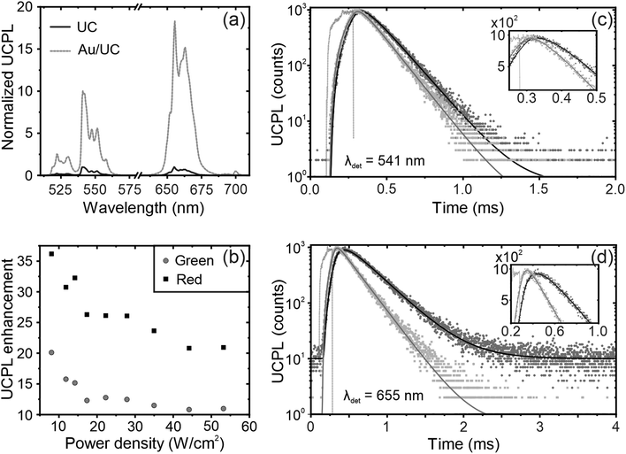 |
| | Fig. 3 (a) UCPL intensity spectra of a reference film (black solid line) and that of the same film over a gold nanoantenna array (grey dashed line) at 53.2 W cm−2 excitation. UCPL intensity is normalized to that of the reference film at 655 nm. (b) UCPL enhancement of green (integrated between 510–575 nm) and red (integrated between 630–695 nm) bands at different excitation powers. A continuous 980 nm laser is used for excitation. (c) and (d) UCPL decay of the reference film (circle symbols) and that of the same film over a gold nanoantenna array (square symbols) monitored at 541 (c) and 655 nm (d). Solid lines are the fits. The instrumental response function is included as a grey dashed line. A pulse 980 nm laser is used for excitation. | |
To analyze its nonlinear behavior, we monitor the UCPL intensity as a function of the excitation power for UC films deposited on a glass substrate and over the nanoantennas. Although the UCPL follows a quadratic dependence (see Fig. S6, ESI†),31,47,53,54 a slight reduction of the slope is observed in the presence of the metal nanoparticles, since the LSPR accelerates the energy transfer from the 2F5/2 energy level of the Yb3+ sensitizers to the 4I11/2 of the Er3+ emitters.31 In addition, the UCPL enhancement decreases with the excitation power density. Specifically, Fig. 3b shows that at low power densities the UCPL enhancement for the red emission band reaches values as high as ∼35-fold at ∼5 W cm−2, but decreases to ∼20-fold at ∼55 W cm−2. Similar behavior is observed for the green band, but with lower factors because the LSPR-mediated UCPL enhancement is lower for the green band. Interestingly, it has been reported that Er3+ emission in the NaYF4 host matrix is not thermally stable, with UCPL intensity decreasing with temperature,9 an effect that may be exacerbated in the presence of nanoantennas due to the temperature rise induced by metal absorption, which may explain the decrease in UCPL enhancement with power. Further analysis shows that the green to red intensity ratio is also affected by the pump power.22,55–57 Although still under debate,56,57 its origin may lay in the different pathways to populate the 4F9/2 energy level of Er3+. At high power, red emission is favored, resulting in a decrease of the green/red ratio. Furthermore, for a given excitation power, the green to red intensity ratio is lower in the presence of the nanoantennas, since the LSPR-mediated enhancement is higher for the red band as discussed above (see Fig. S7 for more details, ESI†).
Time-dependent UCPL characterization
To gain more insight into the underlying mechanism of plasmon-mediated UCPL enhancement, we perform time-dependent measurements. Using a pulsed 980 nm laser as excitation source, we monitor the green and red emission bands at 541 and 655 nm, respectively, associated with the 4S3/2 and 4F9/2 transitions to the 4I15/2 ground state of Er3+. The time dependence of the UCPL intensity can be described using the following equation, which has already been proven useful for describing the PL decay of Er3+ transitions in the NaYF4 matrix:58,59| | 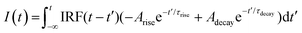 | (2) |
where τrise is the time required to populate the excited energy level and τdecay corresponds to the lifetime of the transition.56 The fitting constants Arise and Adecay must be greater than 0. Eqn (2) also includes the instrumental response function (IRF) to account for the temporal width of the pulsed laser. The fitting results are shown in Fig. 3c, d and Table 1. The residuals of the fits are displayed in Figure S8. The UC reference features a τrise of 52 μs (100 μs) to populate the 4S3/2 (4F9/2) energy level associated with the green (red) emission, respectively. The difference in rise time is due to the different ways of populating these energy levels (see Fig. S5, ESI†). In fact, the green emission results from the pathway 4I15/2 → 4I11/2 → 4F7/2 → 2H11/2 → 4S3/2 → 4I15/2, while there are two possible pathways associated with the red emission, which are: 4I15/2 → 4I11/2 → 4F7/2 → 2H11/2 → 4S3/2 → 4F9/2 → 4I15/2 and 4I15/2 → 4I11/2 → 4I13/2 → 4F9/2 → 4I15/2.56,57 The τdecay is 140 μs (330 μs) for the green (red) transition, in agreement with previous reports.49,59,60 The presence of the nanoantennas enables a reduction in τrise and τdecay for both transitions, as shown in Fig. 3c, d and Table 1. Such a rate enhancement has been previously observed in similar NaYF UCNPs coupled to a layer of gold nanorods.36 Our results indicate that the rise time for the green (red) transition decreases from 52 μs (100 μs) to 37 μs (33 μs). The excited energy level is populated faster when the UCNPs are deposited over the metal nanostructures due to an enhanced Yb3+ excitation rate, which is consistent with the large IIE calculated for ∼980 nm and the enhanced energy transfer between the 2F5/2 energy level of Yb3+ to the 4I11/2 of Er3+.31,61 Also, the metallic nanostructures allow a lifetime reduction.34,37,62 The τdecay reduces from 140 μs (330 μs) to 130 μs (240 μs) for the green (red) transition see Table 1, associated with the fast decay channels typically introduced by metals. The lifetime reduction along with the larger UCPL intensity observed indicate an enhanced radiative decay rate mediated by the coupling between UCNPs and nanoantennas. Finally, we would like to mention that we have extended our study to Ag nanostructures and obtained similar results (see Fig. S9, ESI†). We observe an enhancement of the UCPL as a result of the coupling between UC emission and plasmon resonances supported by either Au or Ag nanoantennas. Ag nanostructures support LSPRs that overlap with both the excitation and emission bands of UCNPs. As a result, the UCPL enhancement reaches values up to ∼50 (80) times for high (low) power density for the red emission band, higher than that observed for Au due to a more effective excitation enhancement. Our results highlight the potential of colloidal lithography to fabricate metallic nanostructures and develop bright, large-area UC coatings in a simple and cost-effective manner.
Table 1 Fitting parameters obtained from the UCPL curves shown in Fig. 3c and d
| Samples |
λ (nm) |
τ
rise (μs) |
τ
decay (μs) |
| UC reference |
541 |
52.0 |
140 |
| Au/UC |
36.9 |
130 |
| UC reference |
655 |
100 |
330 |
| Au/UC |
32.8 |
240 |
Conclusions
We have demonstrated a simple and inexpensive method, based on colloidal lithography, for fabricating a nanoantenna array to enhance the emission of upconverting phosphor nanoparticles. By carefully choosing the shape and size of gold nanostructures, it is possible to engineer LSPRs to match both the excitation and emission bands of NaYF4:Yb3+,Er3+ nanoparticles. At resonance, the electric field intensity in the volume surrounding the metal is significantly increased, which greatly enhances the absorption and emission of nearby UCNPs. As a result, we demonstrate a 20- and 35-fold UCPL enhancement for the green and red emission bands of Er3+, respectively, mainly due to resonant photoexcitation as shown by numerical simulations. Further analysis of the emission dynamics reveals that plasmon-mediated enhancement induces a faster population of the excited energy levels and an enhanced radiative decay rate. Our findings provide new ways to tailor the emission properties of UC nanomaterials without changing the material composition, which could open up avenues for integrating UC coatings into systems of interest for imaging, sensing, or security.
Methods
Synthesis of NaYF4:Yb(20%)Er(2%) (abbreviated as NaYF) NPs
NaYF NPs were synthesized according to a procedure based on another reported elsewhere48 with a modification. Briefly, 1.248 mmol of YCl3.6H2O, 0.32 mmol of YbCl3.6H2O and 0.032 mmol of ErCl3.6H2O were added to a flask containing 20 ml of oleic acid and 48 ml of 1-octadecene. The flask was heated under vacuum at 110 °C for 30 minutes, then N2 was introduced into the system and the temperature was raised to 150 °C and held for 45 minutes. The temperature of the mixture was then cooled to ∼30 °C under N2 flow. A solution of 24 ml methanol containing 6.4 mmol of NH4F and 4 mmol of NaOH was then added. The resulting solution was stirred at this temperature for 3 minutes to achieve homogeneity. Methanol was removed by heating the mixture at ∼65 °C for 30 minutes and then at ∼80 °C for another 30 minutes. The flask was then vacuum degassed at 110 °C for 30 minutes to remove all moisture. N2 was then introduced into the system and the temperature was raised to 300 °C and maintained for 90 minutes. The solution was then cooled down to room temperature. The resulting NPs were precipitated by adding absolute ethanol, collected by centrifugation at 16500 rpm for 20 minutes, washed 3 times with hexane-absolute ethanol (1![[thin space (1/6-em)]](https://www.rsc.org/images/entities/char_2009.gif) :1 v/v), and re-dispersed in chloroform.
:1 v/v), and re-dispersed in chloroform.
Preparation of the metallic nanoantenna array
Nanoantennas were prepared according to a procedure reported elsewhere.63 The first step in the fabrication of the metallic nanoantenna array was the preparation of the colloidal mask. The mask, consisting of a monolayer of polystyrene (PS, diameter of 720 nm) spheres arranged in a hexagonal lattice, was prepared by a wedge evaporation method.63,64 Starting with an aqueous suspension of PS spheres at a concentration of 2.1%, substrates were placed at an angle of 3° with respect to the horizontal and 300 μL of the suspension was deposited. The suspension was then evaporated at room temperature (between 20–30 °C) for 48 hours at 90% humidity. All conditions (concentration, temperature and humidity) were critical to control the evaporation rate, i.e., the deposition of the PS spheres on the substrate. Subsequently, a 100 nm thick Au or Ag layer was deposited by thermal evaporation using a Univex 250 vacuum coating system. Finally, the colloidal mask was mechanically removed by sonication in absolute ethanol for 2 minutes.
Preparation of phosphor nanoparticle thin film
NaYF NPs in chloroform were mixed with poly(acrylic acid) (PAA) dissolved in absolute ethanol at 1:1 v/v ratio. The final concentration was 6.0 and 7.5 mg mL−1 for NaYF NPs and PAA, respectively. The suspension was stirred at room temperature for few days. UCNP films were prepared on metallic nanoantenna arrays by spin-coating 100 μL of such suspension at 2000 rpm for 60 seconds. This process was repeated 3 times. Note that we covered only the part of the substrate surface with metallic nanoantennas. The area without nanostructures was used as a reference.
Morphological and structural characterization
The shape and size of the synthesized NaYF NPs were measured by transmission electron microscopy (TEM) (Philips, model 200CM), while those of the metallic nanoantenna array were examined by atomic force microscopy (AFM, NX10 AFM Park). Silicon cantilevers (Nanosensors) with a resonance frequency around 204–497 kHz and a nominal force constant of 10–130 N m−1 were used. All AFM images were taken in air and in non-contact mode. All images presented here are unprocessed, except for a flatten command used to remove the background slope. Top view images of nanophosphor particle films on areas with and without metallic nanoantennas were obtained by scanning electron microscopy (SEM, Hitachi Model S4800 high-resolution microscope) using a 2 kV voltage and a 10 μA current.
Optical characterization
The ballistic transmittance of nanophosphor films deposited on a glass substrate or a metallic nanoantenna array was measured using a UV-VIS-NIR spectrophotometer (Agilent, Cary 7000), and the specular reflectance was measured using a FTIR spectrophotometer (Bruker IFS-66) attached to a microscope with a 4× objective and 0.1 numerical aperture. In both cases, light was incident on the samples at ∼6°. The spectral dependence and the time dependence of the UCPL intensity was measured using a spectrofluorometer (Edinburgh Instruments, model FLS1000). A 980 nm laser (2 W optical power) was used as the excitation source, operated at maximum power in continuous mode for static UCPL measurements and in pulsed mode (repetition rate of 500 and 250 Hz for green and red emission, respectively; and pulse width of 360 μs) for time-dependent UCPL intensity analysis. Excitation power was adjusted by neutral density filters to study the power dependence of UCPL intensity.
Time dependent UCPL analysis
Time-dependent UCPL results were analyzed using FAST software from Edinburgh, considering the IRF using the exponential component analysis (Reconvolution) model.
Theoretical calculations
Finite-difference in time-domain (FDTD) simulations were performed using a commercial software (Ansys, Lumerical FDTD). The calculations considered a 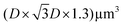 domain, where D is the diameter of the PS spheres (D = 0.72 μm). Periodic boundary conditions were used at the XY boundaries, while perfectly matched layers (PML) were assumed at the vertical boundaries. The refractive index of the glass substrate was assumed to have a constant value of n = 1.51, while a refractive index of n = 1.50 was used for the NaYF films, taking into account the reported refractive index of the particles65 and that of the PAA polymer (n = 1.51). The refractive indices of gold66 and silver67 were also extracted from the literature. Metallic nanoantennas were drawn using open-source CAD software (FreeCAD) and then exported to the FDTD software. The shape of the nanoantenna consisted of ∼100 nm high tetrahedra with slightly rounded edges, ∼200 nm side length. The system was illuminated with a plane wave source, and results for two orthogonal polarizations were simulated and averaged to account for unpolarized light. Reflectance and electric field distribution results were extracted from specific field monitors in the software.
Data availability
Data for this paper are available at Digital CSIC at https://doi.org/10.20350/digitalCSIC/15666.
Conflicts of interest
There are no conflicts to declare.
Acknowledgements
This project is financially supported by the European Research Council (ERC) under the European Union's Horizon 2020 Research and Innovation Programme (NANOPHOM, grant agreement no. 715832). T. T. N. is thankful to grant FJC2020-046006-I funded by MCIN/AEI/10.13039/501100011033 and by the European Union Next Generation EU/PRTR.
References
- J. Zhou, Q. Liu, W. Feng, Y. Sun and F. Li, Chem. Rev., 2015, 115, 395–465 CrossRef CAS PubMed.
- K. Lingeshwar Reddy, R. Balaji, A. Kumar and V. Krishnan, Small, 2018, 14, 1801304 CrossRef PubMed.
- S. Wen, J. Zhou, K. Zheng, A. Bednarkiewicz, X. Liu and D. Jin, Nat. Commun., 2018, 9, 2415 CrossRef PubMed.
- Z. Li and Y. Zhang, Nanotechnology, 2008, 19, 345606 CrossRef PubMed.
- C. Duan, L. Liang, L. Li, R. Zhang and Z. P. Xu, J. Mater. Chem. B, 2018, 6, 192–209 RSC.
- J. Yao, M. Yang and Y. Duan, Chem. Rev., 2014, 114, 6130–6178 CrossRef CAS PubMed.
- A. Gulzar, J. Xu, P. Yang, F. He and L. Xu, Nanoscale, 2017, 9, 12248–12282 RSC.
- J. Dou, B. Chen, G. Liu, X. Dong, W. Yu, J. Wang, Y. Zhang, Z. Li and J. Zhu, J. Rare Earths, 2022, 40, 193–200 CrossRef CAS.
- M. Runowski, N. Stopikowska, D. Szeremeta, S. Goderski, M. Skwierczyńska and S. Lis, ACS Appl. Mater. Interfaces, 2019, 11, 13389–13396 CrossRef CAS PubMed.
- J. Nie, W. Ying, X. Fan, S. Xu, Z. Gao, J. Gu and S. Liu, J. Phys. Chem. C, 2021, 125, 19040–19047 CrossRef CAS.
- P. Zhang, L. Liang and X. Liu, J. Mater. Chem. C, 2021, 9, 16110–16131 RSC.
- F.-L. Meng, J.-J. Wu, E.-F. Zhao, Y.-Z. Zheng, M.-L. Huang, L.-M. Dai, X. Tao and J.-F. Chen, Nanoscale, 2017, 9, 18535–18545 RSC.
- X. Yu, H. Zhang and J. Yu, Aggregate, 2021, 2, 20–34 CrossRef CAS.
- W. Ren, G. Lin, C. Clarke, J. Zhou and D. Jin, Adv. Mater., 2020, 32, 1901430 CrossRef CAS PubMed.
- P. Kumar, S. Singh and B. K. Gupta, Nanoscale, 2016, 8, 14297–14340 RSC.
- N. Kiseleva, D. Busko, B. S. Richards, M. A. Filatov and A. Turshatov, J. Phys. Chem. Lett., 2020, 11, 6560–6566 CrossRef CAS PubMed.
- J.-C. Boyer and F. C. J. M. van Veggel, Nanoscale, 2010, 2, 1417 RSC.
- S. Fan, G. Gao, S. Sun, S. Fan, H. Sun and L. Hu, J. Mater. Chem. C, 2018, 6, 5453–5461 RSC.
- V. Muhr, S. Wilhelm, T. Hirsch and O. S. Wolfbeis, Acc. Chem. Res., 2014, 47, 3481–3493 CrossRef CAS PubMed.
- N. Bogdan, F. Vetrone, G. A. Ozin and J. A. Capobianco, Nano Lett., 2011, 11, 835–840 CrossRef CAS PubMed.
- S. Wilhelm, M. Kaiser, C. Würth, J. Heiland, C. Carrillo-Carrion, V. Muhr, O. S. Wolfbeis, W. J. Parak, U. Resch-Genger and T. Hirsch, Nanoscale, 2015, 7, 1403–1410 RSC.
- W. Gao, Y. Xing, B. Chen, L. Shao, J. Zhang, X. Yan, Q. Han, C. Zhang, L. Liu and J. Dong, J. Alloys Compd., 2023, 936, 168371 CrossRef CAS.
- D. Chen, Y. Yu, F. Huang, H. Lin, P. Huang, A. Yang, Z. Wang and Y. Wang, J. Mater. Chem., 2012, 22, 2632–2640 RSC.
- A. Das, K. Bae and W. Park, Nanophotonics, 2020, 9, 1359–1371 CrossRef CAS.
- X. Qin, A. N. Carneiro Neto, R. L. Longo, Y. Wu, O. L. Malta and X. Liu, J. Phys. Chem. Lett., 2021, 12, 1520–1541 CrossRef CAS PubMed.
- J. Dong, W. Gao, Q. Han, Y. Wang, J. Qi, X. Yan and M. Sun, Rev. Phys., 2019, 4, 100026 CrossRef.
- W. Xu, X. Chen and H. Song, Nano Today, 2017, 17, 54–78 CrossRef CAS.
- D. M. Wu, A. García-Etxarri, A. Salleo and J. A. Dionne, J. Phys. Chem. Lett., 2014, 5, 4020–4031 CrossRef CAS PubMed.
- Y. Wang, Z. Yang, B. Shao, J. Yang, J. Li, J. Qiu and Z. Song, RSC Adv., 2016, 6, 56963–56970 RSC.
-
Plasmonics: From Basics to Advanced Topics, ed. S. Enoch and N. Bonod, Springer Berlin Heidelberg, Berlin, Heidelberg, 2012, vol. 167 Search PubMed.
- T. T. Ngo, G. Lozano and H. Míguez, Mater. Adv., 2022, 3, 4235–4242 RSC.
- H. Chen, Z. Jiang, H. Hu, B. Kang, B. Zhang, X. Mi, L. Guo, C. Zhang, J. Li, J. Lu, L. Yan, Z. Fu, Z. Zhang, H. Zheng and H. Xu, Nat. Photon., 2022, 16, 651–657 CrossRef CAS.
- D. Lu, S. K. Cho, S. Ahn, L. Brun, C. J. Summers and W. Park, ACS Nano, 2014, 8, 7780–7792 CrossRef CAS PubMed.
- A. Das, C. Mao, S. Cho, K. Kim and W. Park, Nat. Commun., 2018, 9, 4828 CrossRef PubMed.
- Q.-C. Sun, H. Mundoor, J. C. Ribot, V. Singh, I. I. Smalyukh and P. Nagpal, Nano Lett., 2014, 14, 101–106 CrossRef CAS PubMed.
- A. L. Feng, M. L. You, L. Tian, S. Singamaneni, M. Liu, Z. Duan, T. J. Lu, F. Xu and M. Lin, Sci. Rep., 2015, 5, 7779 CrossRef CAS PubMed.
- Z. Yin, D. Zhou, W. Xu, S. Cui, X. Chen, H. Wang, S. Xu and H. Song, ACS Appl. Mater. Interfaces, 2016, 8, 11667–11674 CrossRef CAS PubMed.
- Y. Ji, G. Fang, J. Shang, X. Dong, J. Wu, X. Lin, W. Xu and B. Dong, ACS Appl. Mater. Interfaces, 2022, 14, 50045–50054 CrossRef CAS PubMed.
- G. Fang, Y. Ji, Q. Xiao, X. Dong, J. Wu, J. Zou, Y. Xu, W. Xu and B. Dong, J. Mater. Chem. C, 2022, 10, 16430–16438 RSC.
- J. He, W. Zheng, F. Ligmajer, C.-F. Chan, Z. Bao, K.-L. Wong, X. Chen, J. Hao, J. Dai, S.-F. Yu and D. Y. Lei, Light: Sci. Appl., 2017, 6, e16217–e16217 CrossRef CAS PubMed.
- W. Zhang, F. Ding and S. Y. Chou, Adv. Mater., 2012, 24, OP236–OP241 CAS.
- H. Liu, J. Xu, H. Wang, Y. Liu, Q. Ruan, Y. Wu, X. Liu and J. K. W. Yang, Adv. Mater., 2019, 31, 1807900 CrossRef PubMed.
- N. J. Greybush, M. Saboktakin, X. Ye, C. Della Giovampaola, S. J. Oh, N. E. Berry, N. Engheta, C. B. Murray and C. R. Kagan, ACS Nano, 2014, 8, 9482–9491 CrossRef CAS PubMed.
- Y. Gao, S. Murai, K. Shinozaki and K. Tanaka, ACS Appl. Mater. Interfaces, 2023, 15, 9533–9541 CrossRef CAS PubMed.
- Y. Gao, S. Murai, K. Shinozaki, S. Ishii and K. Tanaka, Adv. Opt. Mater., 2021, 9, 2001040 CrossRef CAS.
- W. Luo, F. Xu, A. Li and Z. Sun, Adv. Opt. Mater., 2022, 10, 2102668 CrossRef CAS.
- T. T. Ngo, E. Cabello-Olmo, E. Arroyo, A. I. Becerro, M. Ocaña, G. Lozano and H. Míguez, ACS Appl. Mater. Interfaces, 2021, 13, 30051–30060 CrossRef CAS PubMed.
- Z. Yin, H. Li, W. Xu, S. Cui, D. Zhou, X. Chen, Y. Zhu, G. Qin and H. Song, Adv. Mater., 2016, 28, 2518–2525 CrossRef CAS PubMed.
- R. G. Geitenbeek, P. T. Prins, W. Albrecht, A. van Blaaderen, B. M. Weckhuysen and A. Meijerink, J. Phys. Chem. C, 2017, 121, 3503–3510 CrossRef CAS PubMed.
- J. Liu, Q. Wang, X. Sang, H. Hu, S. Li, D. Zhang, C. Liu, Q. Wang, B. Zhang, W. Wang and F. Song, Nanomaterials, 2021, 11, 1037 CrossRef CAS PubMed.
- C. Mao, K. Min, K. Bae, S. Cho, T. Xu, H. Jeon and W. Park, ACS Photonics, 2019, 6(8), 1882–1888 CrossRef CAS.
- A. Vaskin, R. Kolkowski, A. F. Koenderink and I. Staude, Nanophotonics, 2019, 8, 1151–1198 CrossRef.
- R. E. Joseph and C. Jime, J. Phys. Chem. A, 2019, 123(31), 6799–6811 CrossRef CAS PubMed.
- H. Liu, C. T. Xu, D. Lindgren, H. Xie, D. Thomas, C. Gundlach and S. Andersson-Engels, Nanoscale, 2013, 5, 4770–4775 RSC.
- C. Würth, M. Kaiser, S. Wilhelm, B. Grauel, T. Hirsch and U. Resch-Genger, Nanoscale, 2017, 9, 4283–4294 RSC.
- T. Jung, H. L. Jo, S. H. Nam, B. Yoo, Y. Cho, J. Kim, H. M. Kim, T. Hyeon, Y. D. Suh, H. Lee and K. T. Lee, Phys. Chem. Chem. Phys., 2015, 17, 13201–13205 RSC.
- M. T. Berry and P. S. May, J. Phys. Chem. A, 2015, 119, 9805–9811 CrossRef CAS PubMed.
- J. Kong, X. Shang, W. Zheng, X. Chen, D. Tu, M. Wang, J. Song and J. Qu, J. Phys. Chem. Lett., 2020, 11, 3672–3680 CrossRef CAS PubMed.
- J. Tang, L. Chen, J. Li, Z. Wang, J. Zhang, L. Zhang, Y. Luo and X. Wang, Nanoscale, 2015, 7, 14752–14759 RSC.
- V. Torres Vera, D. Mendez-Gonzalez, D. J. Ramos-Ramos, A. Igalla, M. Laurenti, R. Contreras-Caceres, E. Lopez-Cabarcos, E. Díaz, J. Rubio-Retama, S. Melle and O. G. Calderón, J. Mater. Chem. C, 2021, 9, 8902–8911 RSC.
- D. Lu, C. Mao, S. K. Cho, S. Ahn and W. Park, Sci. Rep., 2016, 6, 18894 CrossRef CAS PubMed.
- Y. Yang, Y. Cong, X. Lin, B. Cao, D. Dong, K. Liu, Y. Xiao, J. Shang, Y. Bao, Y. Liu, G. Fang, Y. Wang, Y. Chen, J. Zhang and B. Dong, J. Mater. Chem. A, 2020, 8, 4040–4048 RSC.
- J. M. Viaña, M. Romero, G. Lozano and H. Míguez, ACS Appl. Nano Mater., 2022, 5, 16242–16249 CrossRef PubMed.
- J. Sun, C. Tang, P. Zhan, Z. Han, Z.-S. Cao and Z.-L. Wang, Langmuir, 2010, 26, 7859–7864 CrossRef CAS PubMed.
- V. I. Sokolov, A. V. Zvyagin, S. M. Igumnov, S. I. Molchanova, M. M. Nazarov, A. V. Nechaev, A. G. Savelyev, A. A. Tyutyunov, E. V. Khaydukov and V. Y. Panchenko, Opt. Spectrosc., 2015, 118, 609–613 CrossRef CAS.
- P. B. Johnson and R. W. Christy, Phys. Rev. B: Solid State, 1972, 6, 4370–4379 CrossRef CAS.
-
E. D. Palik, Handbook of optical constants of solids, Academic press, Orlando San Diego New York, 1985 Search PubMed.
|
| This journal is © The Royal Society of Chemistry 2023 |
Click here to see how this site uses Cookies. View our privacy policy here. 
 Open Access Article
 This Open Access Article is licensed under a Creative Commons Attribution-Non Commercial 3.0 Unported Licence
 ,
Jose M.
Viaña‡
,
Jose M.
Viaña‡


 domain, where D is the diameter of the PS spheres (D = 0.72 μm). Periodic boundary conditions were used at the XY boundaries, while perfectly matched layers (PML) were assumed at the vertical boundaries. The refractive index of the glass substrate was assumed to have a constant value of n = 1.51, while a refractive index of n = 1.50 was used for the NaYF films, taking into account the reported refractive index of the particles65 and that of the PAA polymer (n = 1.51). The refractive indices of gold66 and silver67 were also extracted from the literature. Metallic nanoantennas were drawn using open-source CAD software (FreeCAD) and then exported to the FDTD software. The shape of the nanoantenna consisted of ∼100 nm high tetrahedra with slightly rounded edges, ∼200 nm side length. The system was illuminated with a plane wave source, and results for two orthogonal polarizations were simulated and averaged to account for unpolarized light. Reflectance and electric field distribution results were extracted from specific field monitors in the software.