
 Open Access Article
 This Open Access Article is licensed under a
 Creative Commons Attribution 3.0 Unported Licence
Structural analyses of carbon films deposited at different total mass rates in a hot-filament CVD system†
Mubarak
Ali

Department of Physics, COMSATS University Islamabad, Islamabad Campus, 45550, Park Road, Pakistan. E-mail: mubarak74@mail.com; mubarak60@hotmail.com
First published on 6th October 2023
Abstract
Depositing carbon films rich in the diamond phase was carried out in many studies. However, characterization of the deposited carbon films does not reveal up-to-date information about the structure at all scales. In this work, we deposited carbon films on silicon substrates. To deposit carbon films using a hot-filament chemical vapor deposition technique, the selected total mass flow rates were 200, 300, and 400 sccm. The CH4 concentration was kept constant at 1.5% in all the experiments. The carbon films deposited mainly in the diamond phase show different structures at different total mass flow rates. At 400 sccm, there is a maximum growth rate. The X-ray investigations show that the carbon films were mainly deposited in the diamond and graphite composite structure. Different X-ray peaks are related to the electronic configurations of the graphitic and diamond atoms forming the top-layered surface in a carbon film. The carbon films deposited at different total mass flow rates present new science and engineering. The possible application of the deposited carbon films is also studied. Due to uncertainties in previous studies, the current work strongly suggests re-investigations of the deposition and characterization of carbon films. The results from both the X-ray analysis and field-emission scanning electron microscopy agree with each other. The current study discusses the new underlying science of carbon films. This should, therefore, be exciting and essential for the readers. The study also introduces a new engineering method.
1. Introduction
Syntheses and characterization of carbon films are profitable in many ways. Investigating the deposition of carbon films contributes to the exploration of both basic and applied sciences. In some applications, carbon films deposited under suitable parameters can directly perform their intended functions. The carbon films deposited under different parameters can identify the behavior of materials at different levels.The hot-filament chemical vapor deposition (HF-CVD) system was first proposed in 1982 to synthesize diamond films from CH4 precursors.1 Carbon films possess unique physical and chemical properties, and maintain a broad range of applications. The properties of carbon films deposited using the CVD technique strongly depend on the process parameters.2–5
The influence of the diamond nucleation density on the properties of carbon films is a hot topic. In depositing carbon films, the empirical optimization of the parameters would require millions of experiments.6 Understanding the fundamental chemistry behind depositing carbon films is still far from complete. The chamber configuration in different HF-CVD systems is not the same. The mixture of H2 and CH4 gases is critical in the deposition of carbon films. Using the HF-CVD system under the same setting makes it possible to study the systematic results of the deposited carbon films.
Polycrystalline diamond films deposited using a CVD system have different textures.7–9 The investigations of carbon films deposited by the HF-CVD have mainly focused on diamond nucleation and growth. However, a carbon film deposited by HF-CVD can have other compositions of the carbon depending on the processing conditions.
Nanosheets of graphitic carbon show unusual thermal conductivity.10 Hollow graphitic spheres grown by chemical vapor deposition have improved electrochemical durability.11 Researchers have developed a highly orientated graphitic network grown through chemical vapor deposition as a thermal interface.12
However, these studies discuss the application of carbon films only in terms of the function of the graphite structure. When a carbon film is deposited with both diamond and graphite phases, hybrid applications can be studied. Studies on carbon films are being published routinely in various journals, and a few recently published studies discuss some exciting insights.13–28 When deposited at different thicknesses, the nanometer-thick carbon films do not have the same characteristics.29
Carbon films rich in diamond were deposited on uniquely treated substrates.30 A diamond coating deposited over a cemented carbide tool indicated a novel conversion annealing pretreatment.31 After nanocrystalline diamond deposition, the performance of the composite materials was enhanced.32 The roughness and wear resistance of the diamond coating was improved by increasing the carbon source.33 A conductive diamond for the microscope tip was prepared and characterized.34
The influence of the different total mass flow rates when depositing carbon films still needs to be determined. Carbon films deposited using the HF-CVD technique cover many commercial applications, as evident from the published studies in the field. Without a significant change in the morphology and structure, the thickness of the carbon film is also a prime concern. This study discusses carbon films deposited with diamond and graphite phases under different total mass flow rates.
The microstructure and nanostructure of the deposited carbon films under different total mass flow rates are investigated. In addition to studying the micro-nanostructure, this study presents a detailed analysis of the electronic structure of the carbon atoms deposited in different phases under different total mass flow rates.
2. Experimental details
Silicon substrates were scratched and seeded before placing them in the HF-CVD reactor. Diamond powder with a particle size ∼5 μm was mixed with acetone for preparing the suspension. For scratching, substrates were rotated clockwise and anticlockwise in the diamond suspension for five minutes in each case. The substrates were cleaned with acetone for 10 min after performing the seeding treatment.Diamond powder with a particle size ∼5 μm mixed with acetone gives a satisfactory seeding treatment for silicon wafers. With the particle size ∼5 μm, there was a moderate level of scratching of the silicon surface. This particle size ensures the nucleation of tiny carbon grains in a reasonable time and their uniform distribution throughout the surface.
The inter-wire distance was approx. 8.0 mm. The distance between the filament assembly and substrate surface was approx. 6.0 mm. A tantalum wire was used to construct the filaments. Sixteen wires of tantalum were wound parallelly to maintain the substrate temperature around 850 °C. Different thermocouples were engaged to measure the temperature of the filament and substrate. A new tantalum wire was used to wound the filaments in each experiment. The setting of filaments remained the same in each experiment. Fig. 1 shows the original camera-ready picture of the HF-CVD system.
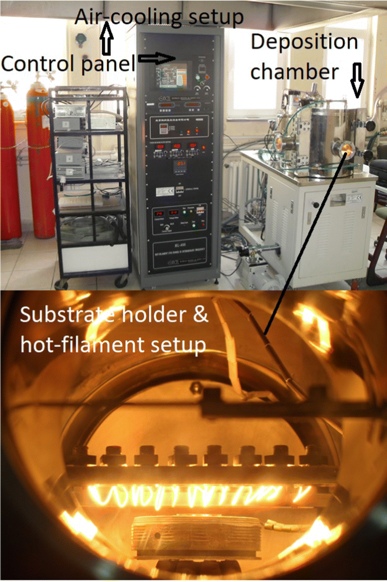 | ||
| Fig. 1 A camera picture of the HF-CVD system and deposition reactor showing the filaments and substrate holder. | ||
A molybdenum plate, 2.0 cm thick, was placed on a water-cooled copper plate. The substrates were loaded on the molybdenum plate to carry out the deposition. Different total mass flow rates were used to deposit the carbon films. In the first experiment, the rate was 200 sccm. In the second experiment, it was 300 sccm, and in the third, it was 400 sccm. In different experiments, the rate of CH4 concentration of 1.5% was kept constant using a high-precision mass flow controller.
By increasing the chamber pressure from 40 torr (at 200 sccm) to 60 torr (at 300 sccm), the filament current reached up to 15 amp. Therefore, at 200 sccm, 40 torr, and 850 °C, the filament current was 260 amps. The filament current reached up to 275 amps at 300 sccm, 60 torr, and 850 °C. The filament current reached up to 290 amps at 400 sccm, 80 torr, and 850 °C. So, the gases entering and leaving the chamber reach the same level. A schematic of the system is given elsewhere.35
The 200 sccm, 300 sccm, and 400 sccm total mass flow rates are enough to study the deposition of the carbon films. To deposit the carbon films, the parameters used in the study were chosen after the execution of many experiments. Therefore, the only selected 200 sccm total mass flow rate in one experiment is better than 100 sccm, 75 sccm, 50 sccm, or 25 sccm. In one experiment, the only selected 400 sccm total mass flow rate is better than 600 sccm, 700 sccm, 900 sccm, or 1000 sccm.
The HF-CVD system did not support the deposition of carbon films at 500 sccm or higher mass flow rates. Maintaining and achieving the set parameters at higher mass flow rates was difficult. Therefore, I stopped the process before reaching the set time. There was also some breakage of hot filaments due to a very high mass flow rate. The carbon films deposited under 100 sccm and 75 sccm total mass flow rates are discussed only in terms of microscopic analyses.
The selection of a total mass flow rate greater than 400 sccm would possibly develop a carbon film rich in graphitic and amorphous phases, thus, not fulfilling the core idea of this paper. At a very high total mass flow rate, keeping the temperature of filaments and substrate constant becomes more crucial in the existing HF-CVD system. The system supports 400 sccm in depositing the carbon film for the required application. Thus, selecting 200 sccm, 300 sccm, and 400 sccm total mass flow rates presents the analyses of more relevant deposited carbon films.
Field emission scanning optical microscopy (FE-SOM) and X-ray reflection (XRR) techniques were used to investigate the deposited carbon films. In the XRR analysis, copper K alpha in-built radiation was used. FE-SOM and XRR were previously known as FE-SEM and XRD.36 The X-ray instrument used was a Philips, Model: PW3710. The microscope used was a JEOL, Model: JSM-7000F.
3. Results and discussion
3.1. Surface morphology
At varying total mass flow rates, the surface morphologies of the carbon films have nearly identical growth trends. However, the size of grains increased with an increase in the total mass flow rate from 200 sccm to 400 sccm, as shown in Fig. 2(a–c). At 300 sccm, the size of tiny grains increases. At 400 sccm, the carbon film shows grains and particles.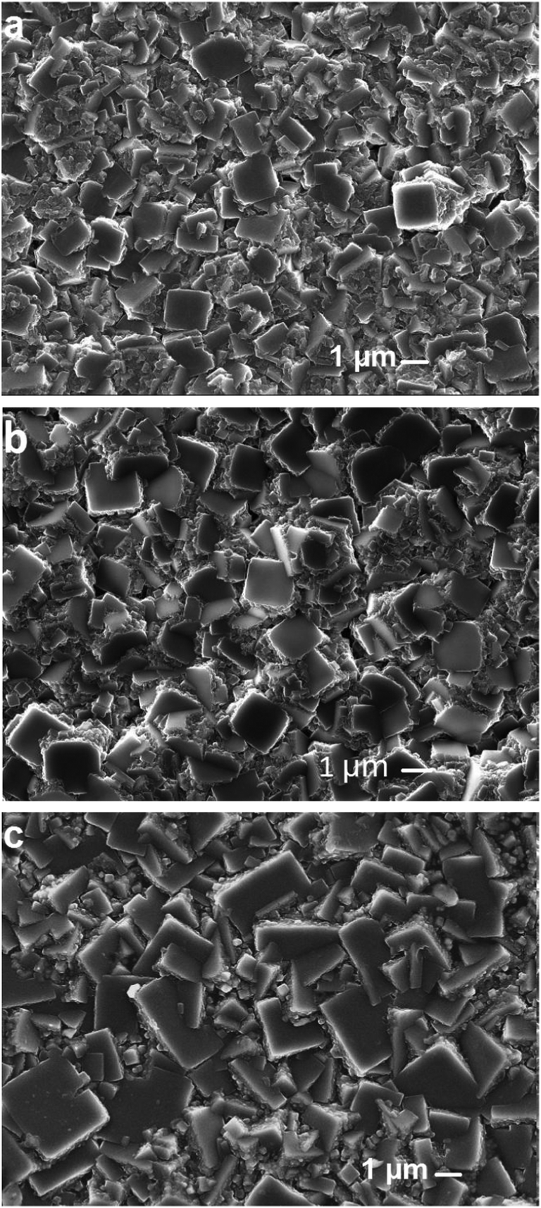 | ||
| Fig. 2 Surface morphology of the carbon films deposited at different total mass flow rates of (a) 200 sccm, (b) 300 sccm, and (c) 400 sccm. | ||
Fig. 2(a–c) also show carbon clusters and carbon dots. The carbon clusters and carbon dots fill the spaces between grains and particles. They are more likely related to the graphitic and amorphous carbon phases. In the surface images, the carbon clusters and carbon dots in the film deposited at 400 sccm are less than the carbon films deposited at 200 and 300 sccm.
The size of grains in Fig. 2(c) reaches the size of the particles. Tiny grains, grains, and particles deposited at different total mass flow rates are mainly in the diamond and graphitic phases, shown in Fig. 2(a–c). In Fig. 2(a–c), the surface morphology of the carbon films deposited at different total mass flow rates is mainly related to the microstructure.
Fig. S1(a–c) (ESI†) show low-magnification microscopic images of the surface morphology of carbon films deposited at 200 sccm, 300 sccm, and 400 sccm. Carbon films deposited at different total mass flow rates cover a large surface area in the low-magnification microscopic images.
The surface morphologies of the carbon films deposited at 100 sccm and 75 sccm are shown in Fig. S2(a) and S3(a) (ESI†), respectively. In these carbon films, the average size of the grain is smaller. The distribution of grains is not uniform. The deposition of carbon films is not over the entire substrate surface.
3.2. Interface study and growth rate
On increasing the total mass flow rate from 200 sccm to 400 sccm, gaseous carbon atoms are converted into diamond at an enhanced rate. In Fig. 3(a–c), the interface images of the carbon films show different growth rates. In Fig. 3(c), a deposited carbon film shows the highest growth rate.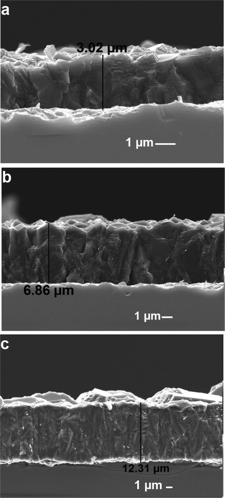 | ||
| Fig. 3 Fractured cross-sectional images of the carbon films deposited at different total mass flow rates of (a) 200, (b) 300, and (c) 400 sccm. | ||
Fig. 3(c) shows the surface in different contrasts. Different contrasts are related to the different phases of carbon. In Fig. 3(c), the diamond phase is higher than the graphite phase. The diamond phase is more related to the faceted grains and particles, whereas the graphite phase is more related to the spherical tiny grains and grains. The distribution of the carbon phases varies from location to location.
The particles of faceted shapes are present in both Fig. 2(c) and 3(c). They are in increased numbers. They are related to the diamond as graphite does not keep the shape of such particles. As a result, the surface per unit diamond phase is more in the carbon film deposited at a 400 sccm total mass flow rate. A graphite phase mainly grows in tiny-sized grains and grains. The carbon clusters and carbon dots are also related to the graphite phase. However, more analysis is required.
The thickness of the carbon film increased from 3.02 μm to 6.86 μm when the total mass flow rate was increased from 200 sccm to 300 sccm, as shown in Fig. 3(b). The thickness of the film increased from 6.86 μm to 12.31 μm when the total mass flow rate was increased from 300 sccm to 400 sccm, as shown in Fig. 3(c).
Increasing the size of tiny grains increases the growth rate of a depositing carbon film. When the total mass flow rate increases from 200 sccm to 300 sccm or 300 sccm to 400 sccm, the CH4 concentration also increases. Therefore, the growth rate of the carbon films deposited at 200 sccm, 300 sccm, and 400 sccm becomes 0.33 μm h−1, 0.76 μm h−1, and 1.37 μm h−1, respectively. An increase in the growth rate of carbon films is mainly related to the transporting CH4 concentration. The dissociation rate of molecular hydrogen becomes high at a higher total mass flow rate. The effect of hydrogen on the structure of carbon films under varying chamber pressures was studied elsewhere.37
The carbon and hydrogen atoms increased in the deposition reactor with an increase in the total mass flow rate. Thus, the carbon film was deposited with an increased growth rate. The carbon atoms and the deposited carbon precursors do not result from CH3, CH2, and CH radicals. The carbon atoms and the deposited carbon precursors resulted from the dissociation of CH4, as discussed elsewhere.37
With an increase in the total mass flow rate, tiny grains increase their size to grow into the size of grains. When the grains are grown to sub-micron or micron size, they are related to the particles, which is the case, as shown in Fig. 3(c).
A new tiny grain can nucleate upon termination of the growing process of a previous grain or particle. It relates to the secondary nucleation process. In the secondary nucleation, a new tiny grain nucleates at the termination of the growth process of the underneath-growing grain or particle. Some details about secondary nucleation are given elsewhere.38 There is a need to re-investigate the nucleation and growth mechanisms of different-sized grains and particles forming the carbon films.
Fractured cross-sectional images of the carbon films deposited at 100 sccm and 75 sccm are shown in Fig. S2(b) and S3(b) (ESI†), respectively. From the fractured cross-sectional images, it is also clear that the distributions of grains are not uniform. The deposition of carbon films is not over the entire substrate surface. Fig. S2(b) and S3(b) (ESI†) also show the thicknesses of the carbon films deposited at total mass flow rates of 100 sccm and 75 sccm, respectively.
3.3. Structural determination of carbon films
Fig. 4(a–c) show the patterns of the carbon films deposited at different total mass flow rates. The peaks at 2θ ∼ 43.9°, 75.3°, 91.5°, and 119.5° are related to the diamond phase. An XRD study is, in fact, an XRR study.36 Thus, new perspectives are required to identify the structures of carbon phases, as discussed below. The glazing incidence angle, GIA, was set at ∼0.5°.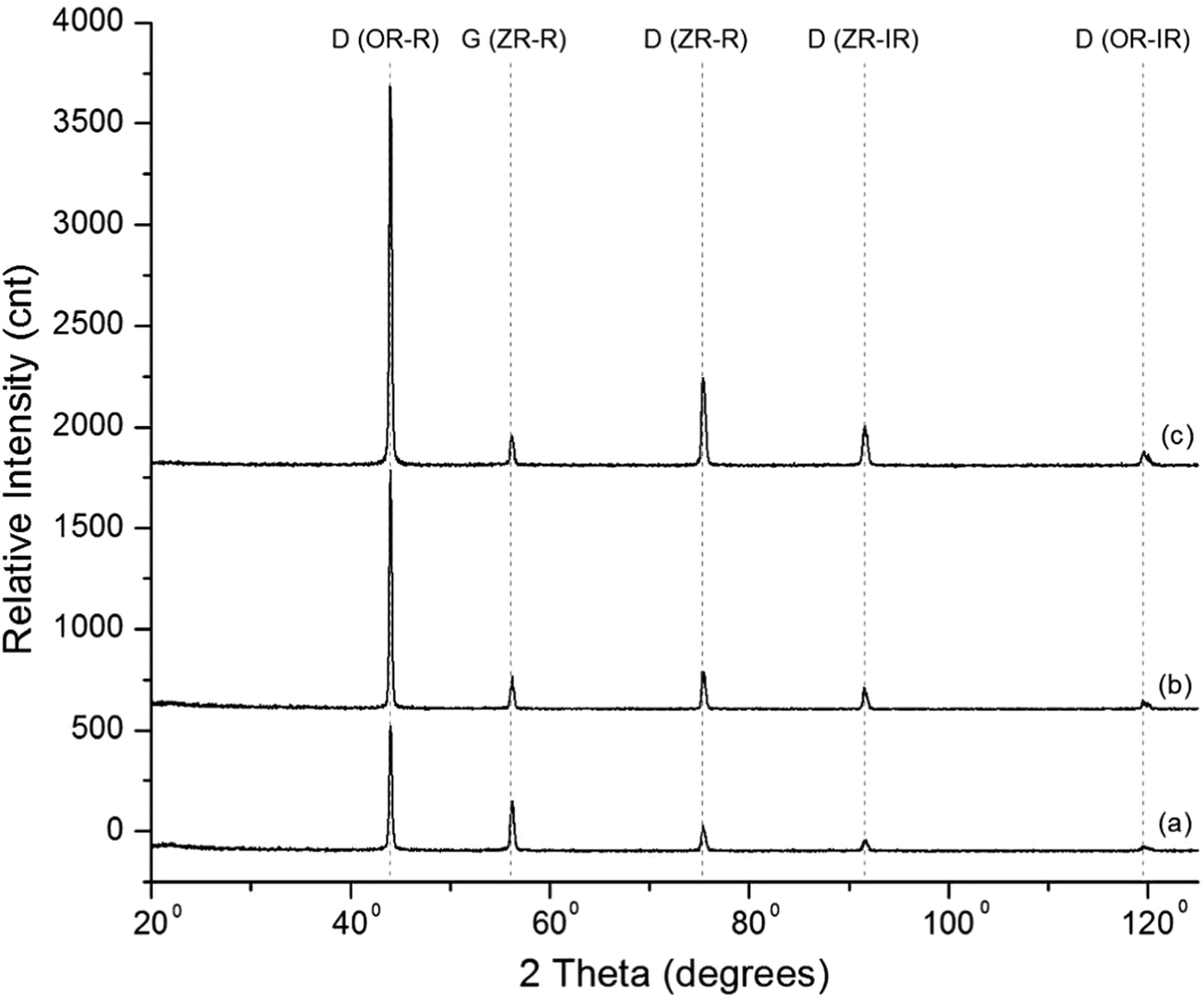 | ||
| Fig. 4 Structural analyses of the carbon films deposited at (a) 200, (b) 300, and (c) 400 sccm total mass flow rates. | ||
The peaks at 2θ ∼ 43.9°, 56.1°, 75.3°, 91.5°, and 119.5° in Fig. 4 are denoted as D (OR-R), G (ZR-R), D (ZR-R), D (ZR-IR), and D (OR-IR), respectively. The first, second, and third peaks are related to the reflection of X-rays from the outer ring electrons of the diamond atoms, zeroth ring electrons of the graphite atoms, and zeroth ring electrons of the diamond atoms, respectively. The fourth and fifth peaks are related to the inverse reflection of X-rays from the zeroth ring electrons of the diamond atoms and the outer ring electrons of the diamond atoms.
Peaks related to different carbon phases show the minimum intensity, average intensity, and highest intensity in Fig. 4(a)–(c), respectively. At a 400 sccm total mass flow rate, the surface morphology of the deposited carbon films has a bigger size of the grains. Many grains in the carbon film deposited at 400 sccm are equal to the size of particles. In the X-ray analysis, front-layered grains and particles of the carbon films only experience the X-rays. The HF-CVD process developed nanoparticles of diamond, and their structural features were compared.39
To observe the changes in the various X-ray patterns of carbon films deposited at different total mass flow rates, replacing 1° with 0.01° or replacing 1° with at least 0.05° along the 2θ scale is required. To identify the difference in the peak formations, FWHM, and intensity of carbon films deposited at different total mass flow rates, a study of some more factors is also needed. Nevertheless, we can still see the different intensities of the peaks in different patterns.
In Fig. 4(c), a carbon film deposited at 400 sccm total mass flow rate shows higher intensities of the peaks. In Fig. 4(b) or (a), a carbon film deposited at 300 or 200 sccm total mass flow rate shows lower intensities of the peaks.
3.4. Underlying mechanisms of depositing carbon films and structural analysis
The thickness of the carbon film further doubled when the total mass flow rate increased from 300 sccm to 400 sccm. It shows that the differently shaped energy bits remained the same in the nucleation and growth of carbon films deposited at different total mass flow rates. But the kinematics and dynamics of the hydrogen and carbon atoms become more effective in producing higher amounts of those energy bits in a carbon film synthesized at 400 sccm.The diamond and graphite growth rate increases at an increasing total mass flow rate from 200 sccm to 400 sccm. The CH4 concentration was at the rate of 1.5%. However, the concentration of CH4 at 400 sccm becomes six, whereas it is three at the 200 sccm total mass flow rate. At 400 sccm, the deposition reactor contains a very high amount of atomic hydrogen. Therefore, a higher amount of the energy bits at 400 sccm is the cause of the improving growth rate of a carbon film.
The size of tiny grains and grains was increased mainly due to increasing the total mass flow rate. More diamond and graphite state atoms experienced the X-rays in a carbon film deposited at 400 sccm. Therefore, the intensity of the peaks becomes high. X-Rays are also a sort of photon. The reflecting X-rays are under the impact of absorption.
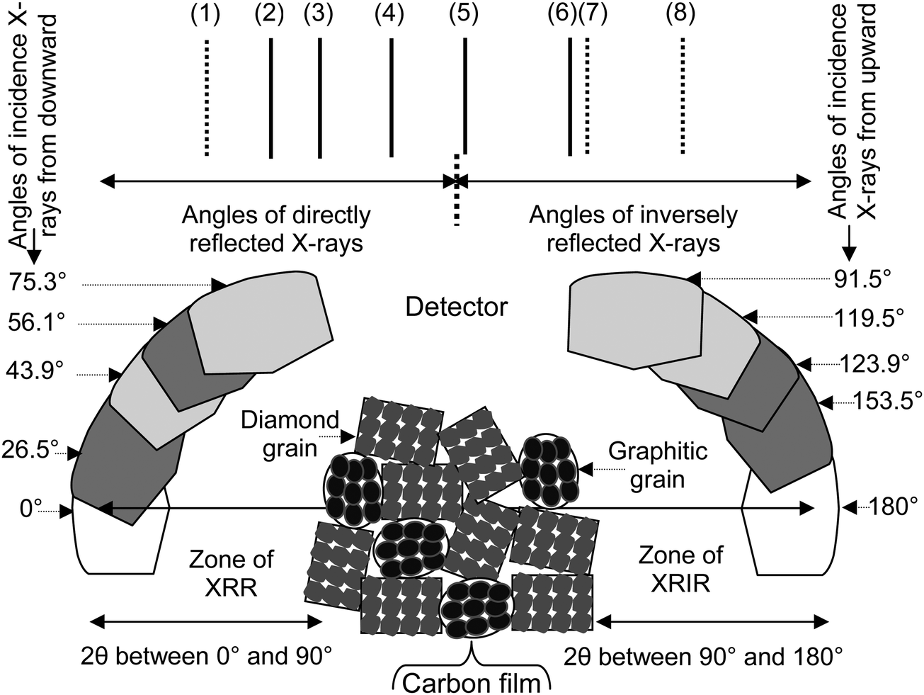
In Fig. 5, the XRR part exists between 0° and 90° of 2θ values, and the X-ray inverse reflection (XRIR) part exists between 90° to 180° of 2θ values. Fig. 5 divides the XRR part and the XRIR part of the pattern. Studies elsewhere36,37 discuss a preliminary detail of an X-ray pattern. The lines at 2θ ∼ 43.9° and 75.3° in Fig. 5 relate to the diamond peaks with the XRR part.
 | ||
| Fig. 5 XRR and XRIR analyses of the deposited carbon film showing different peaks related to the diamond and graphite state atoms. | ||
In Fig. 5, the lines at 2θ ∼ 91.5° and 119.5° belong to the diamond peaks with the XRIR part. In Fig. 5, the lines at 2θ ∼ 26.5° and 56.1° belong to the graphite peaks with the XRR part. In Fig. 5, the lines at 2θ ∼ 123.9° and 153.5° are related to the graphite peaks with the XRIR part. The different patterns shown in Fig. 4 do not show the occurrence of peaks at 2θ ∼ 26.5°, 123.9°, and 153.5°. In Fig. 5, these peaks are denoted by lines and labeled by (1), (7), and (8), respectively.
The peak at 2θ ∼ 43.9° is labeled by (2) in Fig. 5, resulting from the reflection of X-rays from the outer ring electrons of the diamond state atoms. Therefore, the orientation of the outer ring electrons can be ∼43.9° along the north pole from north-sided tips. The peak at 2θ ∼ 75.3° is labeled by (4) in Fig. 5, resulting from the reflection of X-rays from zeroth ring electrons of the diamond state atoms. Therefore, the orientation of the zeroth ring electrons can be ∼75.3° along the north pole from north-sided tips. The peak at 2θ ∼ 91.5° is labeled by (5) in Fig. 5. This peak results from the inverse reflection of X-rays. In this case, zeroth ring electrons of the diamond state atoms participate in dealing with the interactions of X-rays. The peak at 2θ ∼ 119.5° is labeled by (6) in Fig. 5. This peak results from the inverse reflection of X-rays. In this case, the outer ring electrons of the diamond state atoms participate in dealing with the interactions of X-rays.
Zeroth and outer ring electrons existing on the right side to the center of the diamond state atom also keep the same orientations as in the case of zeroth and outer ring electrons existing on the left side to the center of the diamond state atom. However, in the XRIR part, instead of keeping the orientations −75.3° (104.7° = 180°–75.3°) and −43.9° (136.1° = 180°–43.9°), zeroth and outer ring electrons of the diamond state atoms mainly show the orientations 91.5° and 119.5°, respectively. In the XRIR analysis, some inversely but inwardly reflected X-rays making 2θ ∼ 91.5° and 2θ ∼ 119.5° print their intensities at the position of the detector as shown in Fig. 4(a–c).
Thus, the peaks printed in the XRIR part did not obey the originated orientations of the electrons belonging to the zeroth and outer rings of the diamond state atoms.
The peak at 2θ ∼ 26.5° is labeled by (1) in Fig. 5, resulting from the reflection of X-rays from the outer ring electrons of graphite state atoms. The orientation of the outer ring electrons can also be ∼26.5° along the north pole from north-sided tips. The peak at 2θ ∼ 56.1° is labeled by (3) in Fig. 5, resulting in the reflection of X-rays from the zeroth ring electrons of graphite state atoms. The orientation of the zeroth ring electrons can also be ∼56.1° along the north pole from north-sided tips. The peak at 2θ ∼ 123.9° is labeled by (7) in Fig. 5, which can result from the inverse reflection of X-rays from the zeroth ring electrons of graphite state atoms. The peak at 2θ ∼ 153.5° is labeled by (8) in Fig. 5, which can result from the inverse reflection of X-rays from the outer ring electrons of graphite state atoms.
Zeroth and outer ring electrons existing on the right side to the center of the graphite state atom also keep the same orientations as in the case of zeroth and outer ring electrons existing on the left side to the center of the graphite state atom. In the XRIR pattern, instead of keeping the orientations −56.1° (or 123.9° = 180°–56.1°) and −26.5° (153.5° = 180°–26.5°), zeroth ring electrons and outer ring electrons of the graphite state atoms cannot keep their matching orientations like these. The inversely reflected X-rays do not print their intensity at the position of the detector. The non-printing graphitic peaks in the XRIR part can be due to the semisolid behavior of the electrons as the incidence of X-rays is from the upward side.
In the atoms of graphitic grains, outer ring electrons have an orientation nearly adjacent-wise, thereby not experiencing the interaction of X-rays. The peaks at 2θ ∼ 26.5° and 153.5° could not be recognized. The labels (1) and (8) in Fig. 5 are related to these peaks. In each XRR part of the pattern shown in Fig. 4(a–c), a peak at 2θ ∼ 56.1° exists.
However, the peak at 2θ ∼ 123.9° does not exist in Fig. 4(a–c). That peak belongs to the XRIR part of the pattern. In the inverse reflection, X-rays mainly reflect towards the outer sides, and they do not print intensity at the position of the detector.36 The line of the peak shown at 2θ ∼ 123.9° in Fig. 5 is also not recognized in Fig. 4(a–c). This position relates to the peak label by (7) in Fig. 5.
3.5. Application
The deposited carbon films are suitable for hybrid applications. The deposited carbon film can simultaneously work for diamond and graphite applications. The grains and particles related to the diamond phase can build the characteristics to store heat energy as the electronic configuration of the diamond state atom favors dissipating heat. So, the many high-quality diamond grains and particles in the carbon film store heat.The electronic configuration of the diamond state atoms does not favor the propagation of photon energy. As a result, the electronic structure of a diamond is not conducive to photon propagation. A diamond structure cannot keep a consistent interstate electron gap. However, the photons of different wavelengths can travel from the boundaries provided by the grains and particles of the diamond structures or crystals.
The photons of light diffuse for each face of the diamond crystal depending on the orientation of that face. As the diamond structure is a non-favorable electronic structure for propagating photons, the interacting photons can be converted into heat and force.
The heat and force remain confined to each respective face. Each face of the diamond crystal reveals a different texture. A diamond crystal neither works as a mirror nor works as glass. A photon reverts the element of force by interacting with the electronic tip.40 The electrons of silicon atoms can generate photons of wave-like shape.41
Fig. 6 illustrates the propagating photons and dissipating heat energy through the carbon film deposited rich in diamond and graphitic phases. In the hybrid application, there is a simultaneous propagation of photons and dissipation of heat energy. The electrons can work for the photonic bandgap.42 The electrons preserve the atoms, thus not flowing. A photon cannot propagate in the electronic structure of the diamond crystal. A photon can travel through the boundary or defect associated with the diamond film or crystal.
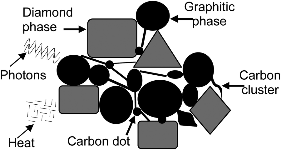 | ||
| Fig. 6 A model study of carbon film showing its hybrid application in terms of propagating photons and dissipating heat. | ||
A diamond crystal stores heat. This property makes the diamond structure create a heat sink. The diamond in the atomic and crystal forms has been discussed elsewhere.43 The single-step method was developed by synthesizing the diamond and titanium interfaces for neural applications elsewhere.44 A review study of carbon films discusses previously explored applications.45
Graphite does not store heat to a large extent. However, it permits the photons to propagate. This property enables the graphite structure to work as an electrode. Here, the electrode propagates the photons rather than conducting the electrons. Photons have the characteristics of a photonic current instead of an electric current.42
The presence of an amorphous carbon phase with diamond and graphite phases can make the carbon film function partially as a heat-dissipating medium and partially as a photon-propagating medium. The deposition of carbon films with tiny grains can effectively emit the field.38 A separate study has discussed graphite and amorphous carbon structures.43 However, the carbon clusters and carbon dots between the graphitic and diamond phases can make the carbon film an ideal candidate for simultaneous heat and photon energy applications.
3.6. Overall discussion
In the HF-CVD technique, where an organic precursor like CH4 is studied along with hydrogen gas, the gaseous carbon first converts into graphitic carbon, followed by the diamond state. At different total mass flow rates, the etched amount of the photon energy gets involved in converting gaseous carbon atoms into graphite state atoms, diamond state atoms, or another state of carbon.A description of the new atomic structures is given elsewhere.46 A recent study discusses the synthesis of a paracrystalline diamond.47 However, the structural investigation of the materials is in the context of the presented detail here. In the earlier studies, the elaborated X-ray pattern's peaks are Bragg peaks.
In the present study, the peaks are labeled by D (OR-R), G (ZR-R), D (ZR-R), D (ZR-IR), and D (OR-IR). In the published studies, the Millers’ indices of the involved lattice planes represent these peaks. Discussions with new insights present the atomic structures of carbon43 and other elements.46 The X-ray diffraction technique is related to the X-ray reflection technique.36 Thus, the deposited carbon films lead to peaks as presented above. Fig. 4 shows the new labels of these peaks.
A reference library or PDF card attached to the X-ray instrument provides information about the lattice planes’ peaks. That information refers to the Miller indices formulation. It is an assumption comprising three steps. In reality, it provides some information about the material under investigation. Bragg peaks do not provide qualitative analysis and add little toward the quantitative description. However, the core aim of the X-ray instrument is to provide a qualitative analysis of the material.
By increasing the total mass flow rate, the pressure and contamination level may rise in the chamber. Therefore, the quality of the carbon film may deteriorate. This indicates that many studies are required to deposit the carbon films with different phases. In an HF-CVD system, optimizing the process parameters for the target application may require many experiments. Furthermore, there is a need to investigate the kinematics and dynamics of converting gaseous carbon atoms into different state carbon atoms.
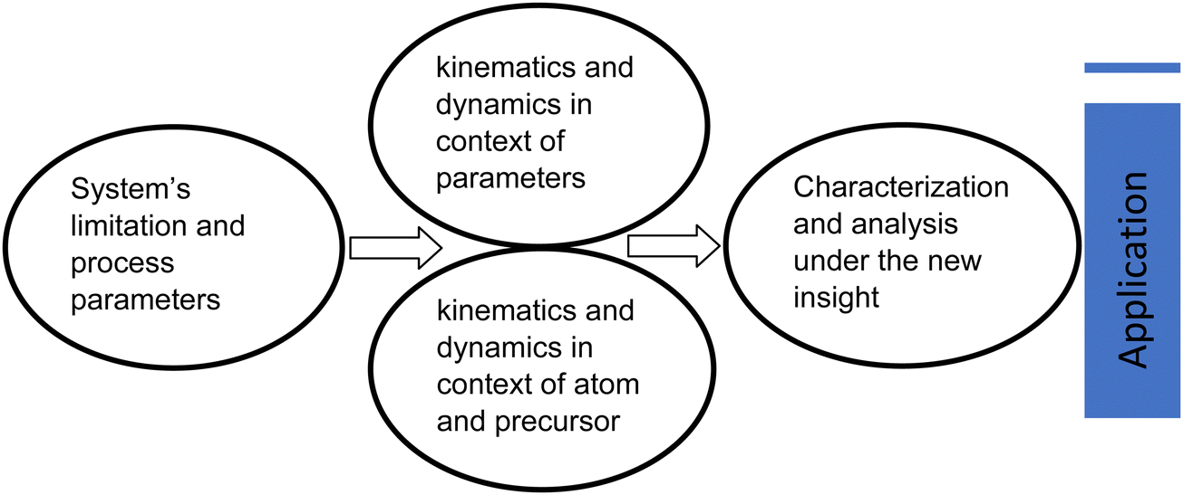
Fig. 7 shows a layout for future perspectives in depositing different carbon-based materials and carbon films. There are various techniques for depositing carbon films.
 | ||
| Fig. 7 A layout for future perspectives in depositing different carbon-based materials or carbon films. | ||
There are different companies for producing a specific deposition system. Even within the same technique, there is more than one model for depositing carbon films. Therefore, it is necessary to check the limitations of a deposition system before performing experiments.
Some parameters also depend on each other while depositing the carbon films in an HF-CVD system. Thus, changing one parameter may alter the kinematics and dynamics of the other parameter not under the planned study. This indicates that depositing carbon films for the target application requires many experiments. Again, there is a need to study the gas dissociation and gas activation processes in the deposition of different carbon films. Thus, the study of chemical thermodynamics is vital in investigating the nucleation and growth of carbon films.
4. Conclusion
The carbon films deposited at different total mass flow rates show different morphologies or microstructures. The size of the grain reaches up to the size of a particle at 400 sccm total flow rate. The thickness of the carbon film increases by increasing the total mass flow rate. It becomes almost double in the carbon film deposited at 300 sccm. It becomes further doubled in the carbon film deposited at 400 sccm. The growth rate of the carbon film deposited at 400 sccm is ∼1.40 μm h−1.X-Rays interact with the electrons of carbon atoms at the top-layered surface, which indicates a higher growth rate of the diamond than the graphite. The increase in the intensity of the diamond peak at 2θ ∼ 43.9° and graphite peak at 2θ ∼ 56.1° validates the increase in the size of diamond and graphite grains at 400 sccm. An XRR pattern defines the diamond structure well. The zeroth and outer ring electrons of diamond atoms are the origin for the peaks at 2θ ∼ 43.9° and 75.3° in the XRR part.
A peak at 2θ ∼ 26.5° does not exist in the XRR pattern. This is due to not having a reflection of X-rays. Outer and zeroth ring electrons of the graphitic carbon atoms are the origin for the peaks at 2θ ∼ 26.5° and 56.1°.
In the inverse reflection of X-rays, the peaks recorded at 2θ ∼ 91.5° and 119.5° are related to the zeroth and outer ring electrons of the diamond state atoms. In the XRIR pattern, the peaks recorded at 2θ ∼ 123.9° and 153.5° are related to the zeroth and outer ring electrons of the graphite state atoms. At these 2θ values, the resulting peaks in the XRIR pattern do not define the structure well due to reflecting X-rays outwardly.
Not defining the structure appropriately under the inverse reflection of X-rays is due to the changed reference of X-ray interaction. In the XRR analysis, the X-ray source follows the trajectory of the arc covering the scale of 2θ between 0° and 90°. However, in the XRIR analysis, the X-ray source does not follow the same line. The X-ray interaction has changed the reference. As a result, a poor structural determination in the XRIR analysis has resulted. X-Rays reflect to show peaks between 0° and 90°, but they inversely reflect to show peaks between 90° and 180°.36
The kinematics and dynamics of the carbon atoms in depositing a carbon film at 400 sccm total mass flow rate become highly efficient. The diamond phase of the carbon film works as a heat sink, whereas the graphite phase of the carbon film works as a photonic propagator. The depositions of carbon films provide opportunities to discuss various physical and chemical aspects from new perspectives.
Author contributions
This publication is by a solo author.Data availability statement
All data generated or analyzed in this study are a part of this article.Conflicts of interest
The author declares no conflicts of interest.Acknowledgements
The award letter ref supported this work by The Scientific and Technological Research Council of Türkiye (TÜBİTAK). # B.02.1.TBT.0.06.01-216.01-677-6045. Mubarak Ali thanks ex-postdoc advisor Professor Dr Mustafa Ürgen, now retired from Istanbul Technical University. Permission to publish the article without the name of Dr Mustafa Ürgen has been granted. Mubarak Ali sincerely thanks Mr Talat ALPAK (ITU) for helping with the field emission scanning optical microscopy.References
- S. Matsumoto, Y. Sato, M. Tsutsumi and N. Setaka, Growth of diamond particles from methane-hydrogen gas, J. Mater. Sci., 1982, 17, 3106–3112 CrossRef.
- P. R. Riley, P. Joshi, J. Narayan and R. J. Narayan, Enhanced nucleation and large-scale growth of CVD diamond via surface-modification of silicon-incorporated diamondlike carbon thin films, Diamond Relat. Mater., 2021, 120, 108630 CrossRef.
- M. Ali, M. Ürgen and M. A. Atta, Effect of surface treatment on hot-filament chemical vapour deposition grown diamond films, J. Phys. D: Appl. Phys., 2012, 45, 045301–045307 CrossRef.
- M. Ali and M. Ürgen, Switching dynamics of morphology-structure in chemically deposited carbon films –A new insight, Carbon, 2017, 122, 653–663 CrossRef.
- Y. Takamori, et al., Insight into temperature impact of Ta filaments on high growth-rate diamond (100) films by hot-filament chemical vapor deposition, Diamond Relat. Mater., 2021, 118, 108515 CrossRef.
- R. T. Anthony, in NATO Advanced Study Institute on Diamond and Diamond-like Films, ed. R. E. Clausing, Plenum, New York, 1991 Search PubMed.
- M. W. Geis, Growth of textured diamond films on foreign substrates from attached seed crystals, Appl. Phys. Lett., 1989, 55, 550 CrossRef.
- C. Wild, N. Herres and P. Koidl, Texture formation in polycrystalline diamond films, J. Appl. Phys., 1990, 68, 973–978 CrossRef.
- K. Tankala, T. DebRoy and M. Alam, Oxidation of diamond films synthesized by hot filament-assisted chemical vapor deposition, J. Mater. Res., 1990, 5, 2483–2489 CrossRef.
- S.-Y. Son, et al., Unusual Thermal Conductivity of Carbon Nanosheets with Self-Emerged Graphitic Carbon Dots, ACS Appl. Mater. Interfaces, 2019, 11, 13616–13623 CrossRef PubMed.
- J. Knossalla, et al., Chemical Vapor Deposition of Hollow Graphitic Spheres for Improved Electrochemical Durability. ACS Applied Energy, Materials, 2021, 4, 5840–5847 Search PubMed.
- L. Zhang, et al., Highly Oriented Graphitic Networks Grown by Chemical Vapor Deposition as Thermal Interface Materials, Ind. Eng. Chem. Res., 2020, 59, 22501–22508 CrossRef.
- C. Wang, X. Wang, X. Shen and F. Sun, Synthesis and evaluation of high-performance diamond films with multilayer structure on printed circuit board drills, Diamond Relat. Mater., 2021, 112, 108249 CrossRef.
- M. Ali, F. Ali, B. Yang and A. Abbas, A comprehensive account of biomedical applications of CVD diamond coatings, J. Phys. D: Appl. Phys., 2021, 54, 443001 CrossRef.
- R. L. Martins, D. D. Damm, E. J. Corat, V. J. Trava-Airoldi and D. M. Barquete, Mitigating residual stress of high-temperature CVD diamond films on vanadium carbide coated steel, J. Vac. Sci. Technol., A, 2021, 39, 013401 CrossRef.
- Z. Zhai, H. Shen, J. Chen and X. Li, Effect of deposition pressure on the properties of amorphous carbon films by hot-filament chemical vapor deposition, J. Mater. Sci.: Mater. Electron., 2019, 30, 10145–10151 CrossRef.
- R. Ahmed, et al., Ultraviolet micro-Raman stress map of polycrystalline diamond grown selectively on silicon substrates using chemical vapor deposition, Appl. Phys. Lett., 2018, 112, 181907 CrossRef.
- P. Joshi, A. Haquea, S. Gupta, R. J. Narayan and J. Narayan, Synthesis of multifunctional microdiamonds on stainless steel substrates by chemical vapor deposition, Carbon, 2021, 171, 739–749 CrossRef.
- M. Y. Jiang, et al., Microstructure and electrochemical properties of nanocrystalline diamond and graphene hybridized films, J. Appl. Phys., 2020, 127, 015301 CrossRef.
- D. Mukherjee, et al., Deposition of diamond films on single crystalline silicon carbide substrates, Diamond Relat. Mater., 2020, 101, 107625 CrossRef.
- Q. Lin, et al., A novel growth model for depositing ultra-nanocrystalline diamond films in CH4/H2 chemistry, Surf. Coat. Technol., 2021, 419, 127280 CrossRef.
- Z. Zhai, H. Shena, J. Chen, Y. Jiang and Q. Tang, Investigation of substrate temperature and cooling method on the properties of amorphous carbon films by hot-filament CVD with acetylene, Carbon, 2017, 117, 322–330 CrossRef.
- H. Wang, C. Wang, X. Wang and F. Sun, Effects of carbon concentration and gas pressure with hydrogen-rich gas chemistry on synthesis and characterizations of HFCVD diamond films on WC-Co substrates, Surf. Coat. Technol., 2021, 409, 126839 CrossRef.
- M. Behera, A. Jena, S. K. Pattnaik, S. Padhi and S. K. Sarangi, The effect of transition-metal seeding powder on deposition and growth of diamond synthesized by hot filament chemical vapor deposition processes on cemented carbide substrates and its characterization, Mater. Chem. Phys., 2020, 256, 123638 CrossRef.
- G. Yan, et al., Mechanical properties and wear behavior of multi-layer diamond films deposited by hot-filament chemical vapor deposition, Appl. Surf. Sci., 2019, 494, 401–411 CrossRef.
- D. Das and M. S. R. Rao, Effects of air annealing on microstructure and optical properties of HFCVD grown microcrystalline diamond thin films, Mater. Today: Proc., 2021, 35, 352–355 CrossRef.
- M. Singh, H. S. Jha and P. Agarwal, Synthesis of vertically aligned carbon nanoflakes by hot-wire chemical vapor deposition: Influence of process pressure and different substrates, Thin Solid Films, 2019, 678, 26–31 CrossRef.
- X. Shen, X. Wang and F. Sun, Fabrication and evaluation of monolayer diamond grinding tools by hot filament chemical vapor deposition method, J. Mater. Process. Technol., 2019, 265, 1–11 CrossRef.
- Z. Chen, et al., The combined use of wrinkling and cracking for the characterization of the mechanical properties of the laser-fabricated nanometer-thick amorphous carbon films, Carbon, 2021, 184, 864–874 CrossRef.
- S. Fan, et al., Effect of pretreatment strategy on the microstructure, mechanical properties and cutting performance of diamond coated hard-metal tools using HFCVD method, Int. J. Refract. Met. Hard Mater., 2021, 101, 105687 CrossRef.
- J. Peng, J. Zeng, Y. Xiao and W. Li, Novel conversion annealing pretreatment for improved deposition of diamond coatings onto WC-Co cemented carbide, J. Alloys Compd., 2022, 893, 162325 CrossRef.
- S. Xiong, et al., Constructing a three-dimensional nano-crystalline diamond network within polymer composites for enhanced thermal conductivity, Nanoscale, 2021, 13, 18657–18664 RSC.
- Y. Wu, Y. Yang, G. Yan and D. Cristea, Wear behaviour of gradient-multilayer diamond coatings deposited on cemented-carbide substrates, Surface Eng., 2022, 38, 507–5143 CrossRef.
- V. Grushko, et al., Preparation and characterization of conductive diamond for a scanning tunneling microscope tip, Diamond Relat. Mater., 2022, 130, 109473 CrossRef.
- M. Ali and I. A. Qazi, Effect of substrate temperature on hot filament chemical vapor deposition grown diamond films, Int. J. Surf. Sci. Eng., 2012, 6, 214–230 CrossRef.
- M. Ali, Qualitative analyses of thin film-based materials validating new structures of atoms, Mater. Today Commun., 2023, 36, 106552 CrossRef.
- M. Ali, Etching of photon energy into binding energy in depositing carbon films at different chamber pressures, J. Mater. Sci.: Mater. Electron., 2023, 34, 1209 CrossRef.
- M. Ali and I.-N. Lin, Phase transitions and critical phenomena of tiny grains carbon films synthesized in microwave-based vapor deposition system, Surf. Interface Anal., 2019, 51, 389–399 CrossRef.
- H.-Y. Kim, D.-S. Kima and N.-M. Hwang, Comparison of diamond nanoparticles captured on the floating and grounded membranes in the hot filament chemical vapor deposition process, RSC Adv., 2021, 11, 5651–5657 RSC.
- M. Ali and I.-N. Lin, Gold Nanostructures and Microstructures with Tunable Aspect Ratios for High-Speed Uni- and Multidirectional Photonic Applications, ACS Appl. Nano Mater., 2020, 3, 9410–9424 CrossRef.
- M. Ali, Heat and Photon Energy Phenomena: Dealing with Matter at Atomic and Electronic Level. (2023), https://www.preprints.org/manuscript/201701.0028/v16.
- M. Ali, Atoms of None of the Elements Ionize While Atoms of Inert Behavior Split by Photonic Current. (2023), https://arxiv.org/abs/1611.05392v32.
- M. Ali, Atomic Structure and Binding of Carbon Atoms. (2023), https://www.preprints.org/manuscript/201801.0036/v17.
- N. Mani, et al., Single-Step Fabrication Method toward 3D Printing Composite Diamond–Titanium Interfaces for Neural Applications, ACS Appl. Mater. Interfaces, 2021, 13, 31474–31484 CrossRef PubMed.
- R. Rathanasamy, et al., Carbon-based Multi-layered Films for Electronic Application: A Review, J. Electron. Mater., 2021, 50, 1845–1892 CrossRef.
- M. Ali, Atoms in Gaseous and Solid States and their Energy and Force Relationships under Transitional Behaviors, 2023 DOI:10.21203/rs.3.rs-88120/v7.
- H. Tang, et al., Synthesis of paracrystalline diamond, Nature, 2021, 599, 605–610 CrossRef PubMed.
Footnote |
| † Electronic supplementary information (ESI) available. See DOI: https://doi.org/10.1039/d3ma00555k |
| This journal is © The Royal Society of Chemistry 2023 |